KR20120085331A - CZTS/Se 전구체 잉크 및 얇은 CZTS/Se 필름과 CZTS/Se-계 광전지의 제조 방법 - Google Patents
CZTS/Se 전구체 잉크 및 얇은 CZTS/Se 필름과 CZTS/Se-계 광전지의 제조 방법 Download PDFInfo
- Publication number
- KR20120085331A KR20120085331A KR1020127016242A KR20127016242A KR20120085331A KR 20120085331 A KR20120085331 A KR 20120085331A KR 1020127016242 A KR1020127016242 A KR 1020127016242A KR 20127016242 A KR20127016242 A KR 20127016242A KR 20120085331 A KR20120085331 A KR 20120085331A
- Authority
- KR
- South Korea
- Prior art keywords
- coated
- czts
- substrate
- nanoparticles
- composition
- Prior art date
Links
- 238000000034 method Methods 0.000 title claims description 46
- 239000002243 precursor Substances 0.000 title abstract description 64
- 239000000976 ink Substances 0.000 title abstract description 57
- 239000010409 thin film Substances 0.000 title abstract description 9
- 239000002105 nanoparticle Substances 0.000 claims abstract description 106
- 150000004770 chalcogenides Chemical class 0.000 claims abstract description 60
- 239000000203 mixture Substances 0.000 claims abstract description 37
- -1 copper zinc tin chalcogenide Chemical class 0.000 claims abstract description 25
- 239000000758 substrate Substances 0.000 claims description 97
- 239000010949 copper Substances 0.000 claims description 77
- 239000011669 selenium Substances 0.000 claims description 65
- LFQSCWFLJHTTHZ-UHFFFAOYSA-N Ethanol Chemical compound CCO LFQSCWFLJHTTHZ-UHFFFAOYSA-N 0.000 claims description 33
- JUJWROOIHBZHMG-UHFFFAOYSA-N Pyridine Chemical compound C1=CC=NC=C1 JUJWROOIHBZHMG-UHFFFAOYSA-N 0.000 claims description 30
- 239000011521 glass Substances 0.000 claims description 29
- VLKZOEOYAKHREP-UHFFFAOYSA-N n-Hexane Chemical compound CCCCCC VLKZOEOYAKHREP-UHFFFAOYSA-N 0.000 claims description 28
- 239000003381 stabilizer Substances 0.000 claims description 25
- 239000011135 tin Substances 0.000 claims description 24
- NINIDFKCEFEMDL-UHFFFAOYSA-N Sulfur Chemical compound [S] NINIDFKCEFEMDL-UHFFFAOYSA-N 0.000 claims description 21
- 229910052751 metal Inorganic materials 0.000 claims description 21
- 239000002184 metal Substances 0.000 claims description 21
- 239000011701 zinc Substances 0.000 claims description 21
- HEDRZPFGACZZDS-UHFFFAOYSA-N Chloroform Chemical compound ClC(Cl)Cl HEDRZPFGACZZDS-UHFFFAOYSA-N 0.000 claims description 20
- XLYOFNOQVPJJNP-UHFFFAOYSA-N water Substances O XLYOFNOQVPJJNP-UHFFFAOYSA-N 0.000 claims description 20
- 238000000576 coating method Methods 0.000 claims description 19
- 239000012530 fluid Substances 0.000 claims description 19
- ZOKXTWBITQBERF-UHFFFAOYSA-N Molybdenum Chemical compound [Mo] ZOKXTWBITQBERF-UHFFFAOYSA-N 0.000 claims description 18
- YXFVVABEGXRONW-UHFFFAOYSA-N Toluene Chemical compound CC1=CC=CC=C1 YXFVVABEGXRONW-UHFFFAOYSA-N 0.000 claims description 18
- 239000011248 coating agent Substances 0.000 claims description 18
- 229910052750 molybdenum Inorganic materials 0.000 claims description 18
- 239000011733 molybdenum Substances 0.000 claims description 18
- 229910052802 copper Inorganic materials 0.000 claims description 15
- UMJSCPRVCHMLSP-UHFFFAOYSA-N pyridine Natural products COC1=CC=CN=C1 UMJSCPRVCHMLSP-UHFFFAOYSA-N 0.000 claims description 15
- 238000000151 deposition Methods 0.000 claims description 14
- 238000010438 heat treatment Methods 0.000 claims description 14
- 229910052718 tin Inorganic materials 0.000 claims description 13
- CSCPPACGZOOCGX-UHFFFAOYSA-N Acetone Chemical compound CC(C)=O CSCPPACGZOOCGX-UHFFFAOYSA-N 0.000 claims description 12
- YMWUJEATGCHHMB-UHFFFAOYSA-N Dichloromethane Chemical compound ClCCl YMWUJEATGCHHMB-UHFFFAOYSA-N 0.000 claims description 12
- 229910052725 zinc Inorganic materials 0.000 claims description 12
- RYGMFSIKBFXOCR-UHFFFAOYSA-N Copper Chemical compound [Cu] RYGMFSIKBFXOCR-UHFFFAOYSA-N 0.000 claims description 11
- ATJFFYVFTNAWJD-UHFFFAOYSA-N Tin Chemical compound [Sn] ATJFFYVFTNAWJD-UHFFFAOYSA-N 0.000 claims description 11
- HCHKCACWOHOZIP-UHFFFAOYSA-N Zinc Chemical compound [Zn] HCHKCACWOHOZIP-UHFFFAOYSA-N 0.000 claims description 11
- UCKMPCXJQFINFW-UHFFFAOYSA-N Sulphide Chemical compound [S-2] UCKMPCXJQFINFW-UHFFFAOYSA-N 0.000 claims description 10
- 239000006185 dispersion Substances 0.000 claims description 10
- BUGBHKTXTAQXES-UHFFFAOYSA-N Selenium Chemical compound [Se] BUGBHKTXTAQXES-UHFFFAOYSA-N 0.000 claims description 9
- HZAXFHJVJLSVMW-UHFFFAOYSA-N 2-Aminoethan-1-ol Chemical compound NCCO HZAXFHJVJLSVMW-UHFFFAOYSA-N 0.000 claims description 8
- IMNFDUFMRHMDMM-UHFFFAOYSA-N N-Heptane Chemical compound CCCCCCC IMNFDUFMRHMDMM-UHFFFAOYSA-N 0.000 claims description 8
- 150000001356 alkyl thiols Chemical class 0.000 claims description 8
- CWERGRDVMFNCDR-UHFFFAOYSA-N thioglycolic acid Chemical compound OC(=O)CS CWERGRDVMFNCDR-UHFFFAOYSA-N 0.000 claims description 8
- 229920001721 polyimide Polymers 0.000 claims description 7
- 239000005361 soda-lime glass Substances 0.000 claims description 7
- 239000002253 acid Substances 0.000 claims description 6
- 150000007513 acids Chemical class 0.000 claims description 5
- 239000000654 additive Substances 0.000 claims description 5
- 150000003973 alkyl amines Chemical class 0.000 claims description 5
- 229920001223 polyethylene glycol Polymers 0.000 claims description 5
- 229920000036 polyvinylpyrrolidone Polymers 0.000 claims description 5
- 235000013855 polyvinylpyrrolidone Nutrition 0.000 claims description 5
- SBIBMFFZSBJNJF-UHFFFAOYSA-N selenium;zinc Chemical compound [Se]=[Zn] SBIBMFFZSBJNJF-UHFFFAOYSA-N 0.000 claims description 5
- 150000003388 sodium compounds Chemical class 0.000 claims description 5
- WRIDQFICGBMAFQ-UHFFFAOYSA-N (E)-8-Octadecenoic acid Natural products CCCCCCCCCC=CCCCCCCC(O)=O WRIDQFICGBMAFQ-UHFFFAOYSA-N 0.000 claims description 4
- LQJBNNIYVWPHFW-UHFFFAOYSA-N 20:1omega9c fatty acid Natural products CCCCCCCCCCC=CCCCCCCCC(O)=O LQJBNNIYVWPHFW-UHFFFAOYSA-N 0.000 claims description 4
- QSBYPNXLFMSGKH-UHFFFAOYSA-N 9-Heptadecensaeure Natural products CCCCCCCC=CCCCCCCCC(O)=O QSBYPNXLFMSGKH-UHFFFAOYSA-N 0.000 claims description 4
- KRKNYBCHXYNGOX-UHFFFAOYSA-K Citrate Chemical compound [O-]C(=O)CC(O)(CC([O-])=O)C([O-])=O KRKNYBCHXYNGOX-UHFFFAOYSA-K 0.000 claims description 4
- 239000005642 Oleic acid Substances 0.000 claims description 4
- ZQPPMHVWECSIRJ-UHFFFAOYSA-N Oleic acid Natural products CCCCCCCCC=CCCCCCCCC(O)=O ZQPPMHVWECSIRJ-UHFFFAOYSA-N 0.000 claims description 4
- 239000002202 Polyethylene glycol Substances 0.000 claims description 4
- XUJNEKJLAYXESH-UHFFFAOYSA-N cysteine Natural products SCC(N)C(O)=O XUJNEKJLAYXESH-UHFFFAOYSA-N 0.000 claims description 4
- 235000018417 cysteine Nutrition 0.000 claims description 4
- 125000000487 histidyl group Chemical group [H]N([H])C(C(=O)O*)C([H])([H])C1=C([H])N([H])C([H])=N1 0.000 claims description 4
- QXJSBBXBKPUZAA-UHFFFAOYSA-N isooleic acid Natural products CCCCCCCC=CCCCCCCCCC(O)=O QXJSBBXBKPUZAA-UHFFFAOYSA-N 0.000 claims description 4
- TVMXDCGIABBOFY-UHFFFAOYSA-N octane Chemical compound CCCCCCCC TVMXDCGIABBOFY-UHFFFAOYSA-N 0.000 claims description 4
- ZQPPMHVWECSIRJ-KTKRTIGZSA-N oleic acid Chemical compound CCCCCCCC\C=C/CCCCCCCC(O)=O ZQPPMHVWECSIRJ-KTKRTIGZSA-N 0.000 claims description 4
- 229920000768 polyamine Polymers 0.000 claims description 4
- 229920005646 polycarboxylate Polymers 0.000 claims description 4
- 159000000000 sodium salts Chemical group 0.000 claims description 3
- 150000004763 sulfides Chemical class 0.000 claims description 3
- 229920000307 polymer substrate Polymers 0.000 claims description 2
- ZWEHNKRNPOVVGH-UHFFFAOYSA-N 2-Butanone Chemical compound CCC(C)=O ZWEHNKRNPOVVGH-UHFFFAOYSA-N 0.000 claims 12
- 150000004771 selenides Chemical class 0.000 claims 5
- 229910019142 PO4 Inorganic materials 0.000 claims 3
- NBIIXXVUZAFLBC-UHFFFAOYSA-K phosphate Chemical compound [O-]P([O-])([O-])=O NBIIXXVUZAFLBC-UHFFFAOYSA-K 0.000 claims 3
- 239000010452 phosphate Substances 0.000 claims 3
- 102000004196 processed proteins & peptides Human genes 0.000 claims 3
- 108090000765 processed proteins & peptides Proteins 0.000 claims 3
- 230000000996 additive effect Effects 0.000 claims 2
- 239000010408 film Substances 0.000 abstract description 44
- 238000004519 manufacturing process Methods 0.000 abstract description 6
- 229910052717 sulfur Inorganic materials 0.000 description 28
- 229910052984 zinc sulfide Inorganic materials 0.000 description 25
- 229910052980 cadmium sulfide Inorganic materials 0.000 description 21
- XLOMVQKBTHCTTD-UHFFFAOYSA-N Zinc monoxide Chemical compound [Zn]=O XLOMVQKBTHCTTD-UHFFFAOYSA-N 0.000 description 20
- 239000000243 solution Substances 0.000 description 20
- IJGRMHOSHXDMSA-UHFFFAOYSA-N Atomic nitrogen Chemical compound N#N IJGRMHOSHXDMSA-UHFFFAOYSA-N 0.000 description 18
- 239000011593 sulfur Substances 0.000 description 18
- 238000000137 annealing Methods 0.000 description 16
- UMGDCJDMYOKAJW-UHFFFAOYSA-N thiourea Chemical compound NC(N)=S UMGDCJDMYOKAJW-UHFFFAOYSA-N 0.000 description 16
- 239000011541 reaction mixture Substances 0.000 description 13
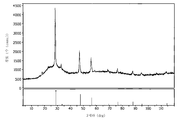
- 238000002441 X-ray diffraction Methods 0.000 description 12
- 239000012299 nitrogen atmosphere Substances 0.000 description 12
- QGLWBTPVKHMVHM-KTKRTIGZSA-N (z)-octadec-9-en-1-amine Chemical compound CCCCCCCC\C=C/CCCCCCCCN QGLWBTPVKHMVHM-KTKRTIGZSA-N 0.000 description 11
- 150000003839 salts Chemical class 0.000 description 11
- 230000015572 biosynthetic process Effects 0.000 description 10
- 238000005119 centrifugation Methods 0.000 description 10
- 229910052955 covellite Inorganic materials 0.000 description 10
- 229910052757 nitrogen Inorganic materials 0.000 description 10
- 239000011787 zinc oxide Substances 0.000 description 10
- 229910052798 chalcogen Inorganic materials 0.000 description 9
- 239000000706 filtrate Substances 0.000 description 9
- 239000000463 material Substances 0.000 description 9
- 239000011734 sodium Substances 0.000 description 9
- XSQUKJJJFZCRTK-UHFFFAOYSA-N Urea Natural products NC(N)=O XSQUKJJJFZCRTK-UHFFFAOYSA-N 0.000 description 8
- 230000008021 deposition Effects 0.000 description 8
- 239000000047 product Substances 0.000 description 8
- 239000002904 solvent Substances 0.000 description 8
- 239000012298 atmosphere Substances 0.000 description 7
- 238000006243 chemical reaction Methods 0.000 description 7
- 239000002245 particle Substances 0.000 description 7
- 229920000642 polymer Polymers 0.000 description 7
- 229910052711 selenium Inorganic materials 0.000 description 7
- 239000004065 semiconductor Substances 0.000 description 7
- 238000004544 sputter deposition Methods 0.000 description 7
- OKKJLVBELUTLKV-UHFFFAOYSA-N Methanol Chemical compound OC OKKJLVBELUTLKV-UHFFFAOYSA-N 0.000 description 6
- 230000008901 benefit Effects 0.000 description 6
- OKIIEJOIXGHUKX-UHFFFAOYSA-L cadmium iodide Chemical compound [Cd+2].[I-].[I-] OKIIEJOIXGHUKX-UHFFFAOYSA-L 0.000 description 6
- 150000001787 chalcogens Chemical class 0.000 description 6
- 238000005507 spraying Methods 0.000 description 6
- 230000002194 synthesizing effect Effects 0.000 description 6
- UUIMDJFBHNDZOW-UHFFFAOYSA-N 2-tert-butylpyridine Chemical compound CC(C)(C)C1=CC=CC=N1 UUIMDJFBHNDZOW-UHFFFAOYSA-N 0.000 description 5
- 150000003346 selenoethers Chemical class 0.000 description 5
- 239000004094 surface-active agent Substances 0.000 description 5
- ZMBHCYHQLYEYDV-UHFFFAOYSA-N trioctylphosphine oxide Chemical compound CCCCCCCCP(=O)(CCCCCCCC)CCCCCCCC ZMBHCYHQLYEYDV-UHFFFAOYSA-N 0.000 description 5
- 239000006096 absorbing agent Substances 0.000 description 4
- 239000000919 ceramic Substances 0.000 description 4
- WNAHIZMDSQCWRP-UHFFFAOYSA-N dodecane-1-thiol Chemical compound CCCCCCCCCCCCS WNAHIZMDSQCWRP-UHFFFAOYSA-N 0.000 description 4
- 229920001343 polytetrafluoroethylene Polymers 0.000 description 4
- 239000004810 polytetrafluoroethylene Substances 0.000 description 4
- 229920006316 polyvinylpyrrolidine Polymers 0.000 description 4
- 238000001556 precipitation Methods 0.000 description 4
- 238000002360 preparation method Methods 0.000 description 4
- 229910052950 sphalerite Inorganic materials 0.000 description 4
- YUKQRDCYNOVPGJ-UHFFFAOYSA-N thioacetamide Chemical compound CC(N)=S YUKQRDCYNOVPGJ-UHFFFAOYSA-N 0.000 description 4
- DLFVBJFMPXGRIB-UHFFFAOYSA-N thioacetamide Natural products CC(N)=O DLFVBJFMPXGRIB-UHFFFAOYSA-N 0.000 description 4
- 238000004627 transmission electron microscopy Methods 0.000 description 4
- FJLUATLTXUNBOT-UHFFFAOYSA-N 1-Hexadecylamine Chemical compound CCCCCCCCCCCCCCCCN FJLUATLTXUNBOT-UHFFFAOYSA-N 0.000 description 3
- WEVYAHXRMPXWCK-UHFFFAOYSA-N Acetonitrile Chemical compound CC#N WEVYAHXRMPXWCK-UHFFFAOYSA-N 0.000 description 3
- 229910021591 Copper(I) chloride Inorganic materials 0.000 description 3
- ZMXDDKWLCZADIW-UHFFFAOYSA-N N,N-Dimethylformamide Chemical compound CN(C)C=O ZMXDDKWLCZADIW-UHFFFAOYSA-N 0.000 description 3
- REYJJPSVUYRZGE-UHFFFAOYSA-N Octadecylamine Chemical compound CCCCCCCCCCCCCCCCCCN REYJJPSVUYRZGE-UHFFFAOYSA-N 0.000 description 3
- PLZVEHJLHYMBBY-UHFFFAOYSA-N Tetradecylamine Chemical compound CCCCCCCCCCCCCCN PLZVEHJLHYMBBY-UHFFFAOYSA-N 0.000 description 3
- 150000001242 acetic acid derivatives Chemical class 0.000 description 3
- 229910052782 aluminium Inorganic materials 0.000 description 3
- XAGFODPZIPBFFR-UHFFFAOYSA-N aluminium Chemical compound [Al] XAGFODPZIPBFFR-UHFFFAOYSA-N 0.000 description 3
- 150000001412 amines Chemical class 0.000 description 3
- 238000000231 atomic layer deposition Methods 0.000 description 3
- 239000011230 binding agent Substances 0.000 description 3
- 229940075417 cadmium iodide Drugs 0.000 description 3
- 239000004020 conductor Substances 0.000 description 3
- 238000001816 cooling Methods 0.000 description 3
- OXBLHERUFWYNTN-UHFFFAOYSA-M copper(I) chloride Chemical compound [Cu]Cl OXBLHERUFWYNTN-UHFFFAOYSA-M 0.000 description 3
- JRBPAEWTRLWTQC-UHFFFAOYSA-N dodecylamine Chemical compound CCCCCCCCCCCCN JRBPAEWTRLWTQC-UHFFFAOYSA-N 0.000 description 3
- 150000004820 halides Chemical class 0.000 description 3
- 238000005286 illumination Methods 0.000 description 3
- 238000010907 mechanical stirring Methods 0.000 description 3
- 150000002739 metals Chemical class 0.000 description 3
- 238000002156 mixing Methods 0.000 description 3
- XTAZYLNFDRKIHJ-UHFFFAOYSA-N n,n-dioctyloctan-1-amine Chemical compound CCCCCCCCN(CCCCCCCC)CCCCCCCC XTAZYLNFDRKIHJ-UHFFFAOYSA-N 0.000 description 3
- 239000007787 solid Substances 0.000 description 3
- 239000000126 substance Substances 0.000 description 3
- FXEIVSYQEOJLBU-UHFFFAOYSA-N 1-$l^{1}-selanylethanimine Chemical compound CC([Se])=N FXEIVSYQEOJLBU-UHFFFAOYSA-N 0.000 description 2
- WHBMMWSBFZVSSR-UHFFFAOYSA-N 3-hydroxybutyric acid Chemical compound CC(O)CC(O)=O WHBMMWSBFZVSSR-UHFFFAOYSA-N 0.000 description 2
- QTBSBXVTEAMEQO-UHFFFAOYSA-N Acetic acid Chemical compound CC(O)=O QTBSBXVTEAMEQO-UHFFFAOYSA-N 0.000 description 2
- VHUUQVKOLVNVRT-UHFFFAOYSA-N Ammonium hydroxide Chemical compound [NH4+].[OH-] VHUUQVKOLVNVRT-UHFFFAOYSA-N 0.000 description 2
- XKRFYHLGVUSROY-UHFFFAOYSA-N Argon Chemical compound [Ar] XKRFYHLGVUSROY-UHFFFAOYSA-N 0.000 description 2
- 238000005481 NMR spectroscopy Methods 0.000 description 2
- URLKBWYHVLBVBO-UHFFFAOYSA-N Para-Xylene Chemical group CC1=CC=C(C)C=C1 URLKBWYHVLBVBO-UHFFFAOYSA-N 0.000 description 2
- 229920001609 Poly(3,4-ethylenedioxythiophene) Polymers 0.000 description 2
- 229910000831 Steel Inorganic materials 0.000 description 2
- PTFCDOFLOPIGGS-UHFFFAOYSA-N Zinc dication Chemical compound [Zn+2] PTFCDOFLOPIGGS-UHFFFAOYSA-N 0.000 description 2
- WAIPAZQMEIHHTJ-UHFFFAOYSA-N [Cr].[Co] Chemical compound [Cr].[Co] WAIPAZQMEIHHTJ-UHFFFAOYSA-N 0.000 description 2
- ZYQNKFKPTUYGMQ-UHFFFAOYSA-N [In]=[Se].[Zn] Chemical compound [In]=[Se].[Zn] ZYQNKFKPTUYGMQ-UHFFFAOYSA-N 0.000 description 2
- 230000003667 anti-reflective effect Effects 0.000 description 2
- 239000008346 aqueous phase Substances 0.000 description 2
- RBHJBMIOOPYDBQ-UHFFFAOYSA-N carbon dioxide;propan-2-one Chemical compound O=C=O.CC(C)=O RBHJBMIOOPYDBQ-UHFFFAOYSA-N 0.000 description 2
- 239000012159 carrier gas Substances 0.000 description 2
- 238000000224 chemical solution deposition Methods 0.000 description 2
- 239000003795 chemical substances by application Substances 0.000 description 2
- 238000005229 chemical vapour deposition Methods 0.000 description 2
- 238000000975 co-precipitation Methods 0.000 description 2
- 229920001577 copolymer Polymers 0.000 description 2
- 238000000354 decomposition reaction Methods 0.000 description 2
- 239000008367 deionised water Substances 0.000 description 2
- 229910021641 deionized water Inorganic materials 0.000 description 2
- 238000003618 dip coating Methods 0.000 description 2
- 239000002270 dispersing agent Substances 0.000 description 2
- 238000004090 dissolution Methods 0.000 description 2
- 238000001548 drop coating Methods 0.000 description 2
- 238000001035 drying Methods 0.000 description 2
- 238000009713 electroplating Methods 0.000 description 2
- 238000001704 evaporation Methods 0.000 description 2
- 230000008020 evaporation Effects 0.000 description 2
- 238000001914 filtration Methods 0.000 description 2
- 239000007789 gas Substances 0.000 description 2
- 239000012535 impurity Substances 0.000 description 2
- 229910052738 indium Inorganic materials 0.000 description 2
- APFVFJFRJDLVQX-UHFFFAOYSA-N indium atom Chemical compound [In] APFVFJFRJDLVQX-UHFFFAOYSA-N 0.000 description 2
- XEEYBQQBJWHFJM-UHFFFAOYSA-N iron Substances [Fe] XEEYBQQBJWHFJM-UHFFFAOYSA-N 0.000 description 2
- 229910052742 iron Inorganic materials 0.000 description 2
- PNHVEGMHOXTHMW-UHFFFAOYSA-N magnesium;zinc;oxygen(2-) Chemical compound [O-2].[O-2].[Mg+2].[Zn+2] PNHVEGMHOXTHMW-UHFFFAOYSA-N 0.000 description 2
- 150000002823 nitrates Chemical class 0.000 description 2
- 239000011368 organic material Substances 0.000 description 2
- 229910052760 oxygen Inorganic materials 0.000 description 2
- 238000005240 physical vapour deposition Methods 0.000 description 2
- 229920003023 plastic Polymers 0.000 description 2
- 239000004033 plastic Substances 0.000 description 2
- 229920000747 poly(lactic acid) Polymers 0.000 description 2
- 229920001467 poly(styrenesulfonates) Polymers 0.000 description 2
- 239000001267 polyvinylpyrrolidone Substances 0.000 description 2
- 239000000843 powder Substances 0.000 description 2
- 238000007639 printing Methods 0.000 description 2
- 238000001004 secondary ion mass spectrometry Methods 0.000 description 2
- IYKVLICPFCEZOF-UHFFFAOYSA-N selenourea Chemical compound NC(N)=[Se] IYKVLICPFCEZOF-UHFFFAOYSA-N 0.000 description 2
- 229910052708 sodium Inorganic materials 0.000 description 2
- 238000000527 sonication Methods 0.000 description 2
- 238000004528 spin coating Methods 0.000 description 2
- 229910001220 stainless steel Inorganic materials 0.000 description 2
- 239000010935 stainless steel Substances 0.000 description 2
- 239000010959 steel Substances 0.000 description 2
- 239000011550 stock solution Substances 0.000 description 2
- 239000000725 suspension Substances 0.000 description 2
- UQMZPFKLYHOJDL-UHFFFAOYSA-N zinc;cadmium(2+);disulfide Chemical compound [S-2].[S-2].[Zn+2].[Cd+2] UQMZPFKLYHOJDL-UHFFFAOYSA-N 0.000 description 2
- RKDVKSZUMVYZHH-UHFFFAOYSA-N 1,4-dioxane-2,5-dione Chemical compound O=C1COC(=O)CO1 RKDVKSZUMVYZHH-UHFFFAOYSA-N 0.000 description 1
- GKWLILHTTGWKLQ-UHFFFAOYSA-N 2,3-dihydrothieno[3,4-b][1,4]dioxine Chemical compound O1CCOC2=CSC=C21 GKWLILHTTGWKLQ-UHFFFAOYSA-N 0.000 description 1
- NRGGMCIBEHEAIL-UHFFFAOYSA-N 2-ethylpyridine Chemical compound CCC1=CC=CC=N1 NRGGMCIBEHEAIL-UHFFFAOYSA-N 0.000 description 1
- BSKHPKMHTQYZBB-UHFFFAOYSA-N 2-methylpyridine Chemical compound CC1=CC=CC=N1 BSKHPKMHTQYZBB-UHFFFAOYSA-N 0.000 description 1
- HVLUYXIJZLDNIS-UHFFFAOYSA-N 2-thiophen-2-ylethanamine Chemical compound NCCC1=CC=CS1 HVLUYXIJZLDNIS-UHFFFAOYSA-N 0.000 description 1
- WUPHOULIZUERAE-UHFFFAOYSA-N 3-(oxolan-2-yl)propanoic acid Chemical compound OC(=O)CCC1CCCO1 WUPHOULIZUERAE-UHFFFAOYSA-N 0.000 description 1
- 229910018072 Al 2 O 3 Inorganic materials 0.000 description 1
- OKTJSMMVPCPJKN-UHFFFAOYSA-N Carbon Chemical compound [C] OKTJSMMVPCPJKN-UHFFFAOYSA-N 0.000 description 1
- CURLTUGMZLYLDI-UHFFFAOYSA-N Carbon dioxide Chemical compound O=C=O CURLTUGMZLYLDI-UHFFFAOYSA-N 0.000 description 1
- 229910004613 CdTe Inorganic materials 0.000 description 1
- 239000004971 Cross linker Substances 0.000 description 1
- RWSOTUBLDIXVET-UHFFFAOYSA-N Dihydrogen sulfide Chemical compound S RWSOTUBLDIXVET-UHFFFAOYSA-N 0.000 description 1
- KMTRUDSVKNLOMY-UHFFFAOYSA-N Ethylene carbonate Chemical compound O=C1OCCO1 KMTRUDSVKNLOMY-UHFFFAOYSA-N 0.000 description 1
- 239000004606 Fillers/Extenders Substances 0.000 description 1
- GYHNNYVSQQEPJS-UHFFFAOYSA-N Gallium Chemical compound [Ga] GYHNNYVSQQEPJS-UHFFFAOYSA-N 0.000 description 1
- DGAQECJNVWCQMB-PUAWFVPOSA-M Ilexoside XXIX Chemical compound C[C@@H]1CC[C@@]2(CC[C@@]3(C(=CC[C@H]4[C@]3(CC[C@@H]5[C@@]4(CC[C@@H](C5(C)C)OS(=O)(=O)[O-])C)C)[C@@H]2[C@]1(C)O)C)C(=O)O[C@H]6[C@@H]([C@H]([C@@H]([C@H](O6)CO)O)O)O.[Na+] DGAQECJNVWCQMB-PUAWFVPOSA-M 0.000 description 1
- KWYHDKDOAIKMQN-UHFFFAOYSA-N N,N,N',N'-tetramethylethylenediamine Chemical compound CN(C)CCN(C)C KWYHDKDOAIKMQN-UHFFFAOYSA-N 0.000 description 1
- 229920001244 Poly(D,L-lactide) Polymers 0.000 description 1
- 229920002845 Poly(methacrylic acid) Polymers 0.000 description 1
- 229920000954 Polyglycolide Polymers 0.000 description 1
- 229920000388 Polyphosphate Polymers 0.000 description 1
- 229910006404 SnO 2 Inorganic materials 0.000 description 1
- VMHLLURERBWHNL-UHFFFAOYSA-M Sodium acetate Chemical compound [Na+].CC([O-])=O VMHLLURERBWHNL-UHFFFAOYSA-M 0.000 description 1
- 229960000583 acetic acid Drugs 0.000 description 1
- 230000002378 acidificating effect Effects 0.000 description 1
- 238000004220 aggregation Methods 0.000 description 1
- 230000002776 aggregation Effects 0.000 description 1
- 150000001298 alcohols Chemical class 0.000 description 1
- 150000001335 aliphatic alkanes Chemical class 0.000 description 1
- QGZKDVFQNNGYKY-UHFFFAOYSA-N ammonia Natural products N QGZKDVFQNNGYKY-UHFFFAOYSA-N 0.000 description 1
- 239000000908 ammonium hydroxide Substances 0.000 description 1
- 239000003963 antioxidant agent Substances 0.000 description 1
- 229910052786 argon Inorganic materials 0.000 description 1
- 230000008033 biological extinction Effects 0.000 description 1
- 230000005540 biological transmission Effects 0.000 description 1
- 229910052793 cadmium Inorganic materials 0.000 description 1
- QCUOBSQYDGUHHT-UHFFFAOYSA-L cadmium sulfate Chemical compound [Cd+2].[O-]S([O-])(=O)=O QCUOBSQYDGUHHT-UHFFFAOYSA-L 0.000 description 1
- 229910000331 cadmium sulfate Inorganic materials 0.000 description 1
- 229910052799 carbon Inorganic materials 0.000 description 1
- 235000011089 carbon dioxide Nutrition 0.000 description 1
- 230000015556 catabolic process Effects 0.000 description 1
- 239000003153 chemical reaction reagent Substances 0.000 description 1
- 150000001805 chlorine compounds Chemical class 0.000 description 1
- 229910052804 chromium Inorganic materials 0.000 description 1
- KRKNYBCHXYNGOX-UHFFFAOYSA-N citric acid Chemical group OC(=O)CC(O)(C(O)=O)CC(O)=O KRKNYBCHXYNGOX-UHFFFAOYSA-N 0.000 description 1
- 238000010549 co-Evaporation Methods 0.000 description 1
- 150000001875 compounds Chemical class 0.000 description 1
- 229920001940 conductive polymer Polymers 0.000 description 1
- HVMJUDPAXRRVQO-UHFFFAOYSA-N copper indium Chemical compound [Cu].[In] HVMJUDPAXRRVQO-UHFFFAOYSA-N 0.000 description 1
- WILFBXOGIULNAF-UHFFFAOYSA-N copper sulfanylidenetin zinc Chemical compound [Sn]=S.[Zn].[Cu] WILFBXOGIULNAF-UHFFFAOYSA-N 0.000 description 1
- ORTQZVOHEJQUHG-UHFFFAOYSA-L copper(II) chloride Chemical compound Cl[Cu]Cl ORTQZVOHEJQUHG-UHFFFAOYSA-L 0.000 description 1
- MPTQRFCYZCXJFQ-UHFFFAOYSA-L copper(II) chloride dihydrate Chemical compound O.O.[Cl-].[Cl-].[Cu+2] MPTQRFCYZCXJFQ-UHFFFAOYSA-L 0.000 description 1
- XTVVROIMIGLXTD-UHFFFAOYSA-N copper(II) nitrate Chemical compound [Cu+2].[O-][N+]([O-])=O.[O-][N+]([O-])=O XTVVROIMIGLXTD-UHFFFAOYSA-N 0.000 description 1
- 238000005260 corrosion Methods 0.000 description 1
- 230000007797 corrosion Effects 0.000 description 1
- VTXVGVNLYGSIAR-UHFFFAOYSA-N decane-1-thiol Chemical compound CCCCCCCCCCS VTXVGVNLYGSIAR-UHFFFAOYSA-N 0.000 description 1
- 238000010908 decantation Methods 0.000 description 1
- 238000006731 degradation reaction Methods 0.000 description 1
- 239000002274 desiccant Substances 0.000 description 1
- 238000010586 diagram Methods 0.000 description 1
- 238000007607 die coating method Methods 0.000 description 1
- 238000007606 doctor blade method Methods 0.000 description 1
- ZTPZXOVJDMQVIK-UHFFFAOYSA-N dodecane-1-selenol Chemical compound CCCCCCCCCCCC[SeH] ZTPZXOVJDMQVIK-UHFFFAOYSA-N 0.000 description 1
- 238000004070 electrodeposition Methods 0.000 description 1
- 238000005566 electron beam evaporation Methods 0.000 description 1
- 238000010894 electron beam technology Methods 0.000 description 1
- 238000001493 electron microscopy Methods 0.000 description 1
- 239000003995 emulsifying agent Substances 0.000 description 1
- 238000005516 engineering process Methods 0.000 description 1
- 150000002148 esters Chemical class 0.000 description 1
- 150000002170 ethers Chemical class 0.000 description 1
- 239000000945 filler Substances 0.000 description 1
- 229910052733 gallium Inorganic materials 0.000 description 1
- 239000012362 glacial acetic acid Substances 0.000 description 1
- 229920001519 homopolymer Polymers 0.000 description 1
- 150000004679 hydroxides Chemical class 0.000 description 1
- AKUCEXGLFUSJCD-UHFFFAOYSA-N indium(3+);selenium(2-) Chemical compound [Se-2].[Se-2].[Se-2].[In+3].[In+3] AKUCEXGLFUSJCD-UHFFFAOYSA-N 0.000 description 1
- AMGQUBHHOARCQH-UHFFFAOYSA-N indium;oxotin Chemical compound [In].[Sn]=O AMGQUBHHOARCQH-UHFFFAOYSA-N 0.000 description 1
- 239000003112 inhibitor Substances 0.000 description 1
- 238000007641 inkjet printing Methods 0.000 description 1
- 229910010272 inorganic material Inorganic materials 0.000 description 1
- 239000011147 inorganic material Substances 0.000 description 1
- 150000002576 ketones Chemical class 0.000 description 1
- 239000003446 ligand Substances 0.000 description 1
- 238000005259 measurement Methods 0.000 description 1
- 238000007760 metering rod coating Methods 0.000 description 1
- 125000005395 methacrylic acid group Chemical group 0.000 description 1
- 239000004530 micro-emulsion Substances 0.000 description 1
- 150000004767 nitrides Chemical class 0.000 description 1
- 150000002825 nitriles Chemical class 0.000 description 1
- 231100000252 nontoxic Toxicity 0.000 description 1
- 230000003000 nontoxic effect Effects 0.000 description 1
- 238000012856 packing Methods 0.000 description 1
- 239000008188 pellet Substances 0.000 description 1
- 239000012071 phase Substances 0.000 description 1
- 229920000515 polycarbonate Polymers 0.000 description 1
- 239000004417 polycarbonate Substances 0.000 description 1
- 229920000570 polyether Polymers 0.000 description 1
- 229920000193 polymethacrylate Polymers 0.000 description 1
- 239000001205 polyphosphate Substances 0.000 description 1
- 235000011176 polyphosphates Nutrition 0.000 description 1
- 229920000379 polypropylene carbonate Polymers 0.000 description 1
- 238000012545 processing Methods 0.000 description 1
- 238000004549 pulsed laser deposition Methods 0.000 description 1
- WHMDPDGBKYUEMW-UHFFFAOYSA-N pyridine-2-thiol Chemical compound SC1=CC=CC=N1 WHMDPDGBKYUEMW-UHFFFAOYSA-N 0.000 description 1
- HNJBEVLQSNELDL-UHFFFAOYSA-N pyrrolidin-2-one Chemical compound O=C1CCCN1 HNJBEVLQSNELDL-UHFFFAOYSA-N 0.000 description 1
- 238000004151 rapid thermal annealing Methods 0.000 description 1
- 238000001226 reprecipitation Methods 0.000 description 1
- 238000007761 roller coating Methods 0.000 description 1
- 150000003958 selenols Chemical class 0.000 description 1
- 125000004469 siloxy group Chemical group [SiH3]O* 0.000 description 1
- 239000001632 sodium acetate Substances 0.000 description 1
- 235000017281 sodium acetate Nutrition 0.000 description 1
- 238000003980 solgel method Methods 0.000 description 1
- 238000003746 solid phase reaction Methods 0.000 description 1
- 239000012265 solid product Substances 0.000 description 1
- 238000010671 solid-state reaction Methods 0.000 description 1
- 238000004611 spectroscopical analysis Methods 0.000 description 1
- 239000007921 spray Substances 0.000 description 1
- 238000005118 spray pyrolysis Methods 0.000 description 1
- 238000010561 standard procedure Methods 0.000 description 1
- 229940071182 stannate Drugs 0.000 description 1
- 238000003756 stirring Methods 0.000 description 1
- MLKXDPUZXIRXEP-MFOYZWKCSA-N sulindac Chemical compound CC1=C(CC(O)=O)C2=CC(F)=CC=C2\C1=C/C1=CC=C(S(C)=O)C=C1 MLKXDPUZXIRXEP-MFOYZWKCSA-N 0.000 description 1
- 239000006228 supernatant Substances 0.000 description 1
- 238000003786 synthesis reaction Methods 0.000 description 1
- 238000005287 template synthesis Methods 0.000 description 1
- 238000012360 testing method Methods 0.000 description 1
- 238000002207 thermal evaporation Methods 0.000 description 1
- 239000002562 thickening agent Substances 0.000 description 1
- KHMOASUYFVRATF-UHFFFAOYSA-J tin(4+);tetrachloride;pentahydrate Chemical compound O.O.O.O.O.Cl[Sn](Cl)(Cl)Cl KHMOASUYFVRATF-UHFFFAOYSA-J 0.000 description 1
- HPGGPRDJHPYFRM-UHFFFAOYSA-J tin(iv) chloride Chemical compound Cl[Sn](Cl)(Cl)Cl HPGGPRDJHPYFRM-UHFFFAOYSA-J 0.000 description 1
- GPRLSGONYQIRFK-MNYXATJNSA-N triton Chemical compound [3H+] GPRLSGONYQIRFK-MNYXATJNSA-N 0.000 description 1
- 229910052721 tungsten Inorganic materials 0.000 description 1
- 229910052720 vanadium Inorganic materials 0.000 description 1
- 238000005406 washing Methods 0.000 description 1
- UGZADUVQMDAIAO-UHFFFAOYSA-L zinc hydroxide Chemical compound [OH-].[OH-].[Zn+2] UGZADUVQMDAIAO-UHFFFAOYSA-L 0.000 description 1
- 229910021511 zinc hydroxide Inorganic materials 0.000 description 1
- 229940007718 zinc hydroxide Drugs 0.000 description 1
Images

Classifications
-
- H—ELECTRICITY
- H01—ELECTRIC ELEMENTS
- H01L—SEMICONDUCTOR DEVICES NOT COVERED BY CLASS H10
- H01L21/00—Processes or apparatus adapted for the manufacture or treatment of semiconductor or solid state devices or of parts thereof
- H01L21/02—Manufacture or treatment of semiconductor devices or of parts thereof
- H01L21/02104—Forming layers
- H01L21/02365—Forming inorganic semiconducting materials on a substrate
- H01L21/02518—Deposited layers
- H01L21/02521—Materials
- H01L21/02568—Chalcogenide semiconducting materials not being oxides, e.g. ternary compounds
-
- H—ELECTRICITY
- H01—ELECTRIC ELEMENTS
- H01L—SEMICONDUCTOR DEVICES NOT COVERED BY CLASS H10
- H01L31/00—Semiconductor devices sensitive to infrared radiation, light, electromagnetic radiation of shorter wavelength or corpuscular radiation and specially adapted either for the conversion of the energy of such radiation into electrical energy or for the control of electrical energy by such radiation; Processes or apparatus specially adapted for the manufacture or treatment thereof or of parts thereof; Details thereof
- H01L31/04—Semiconductor devices sensitive to infrared radiation, light, electromagnetic radiation of shorter wavelength or corpuscular radiation and specially adapted either for the conversion of the energy of such radiation into electrical energy or for the control of electrical energy by such radiation; Processes or apparatus specially adapted for the manufacture or treatment thereof or of parts thereof; Details thereof adapted as photovoltaic [PV] conversion devices
-
- C—CHEMISTRY; METALLURGY
- C23—COATING METALLIC MATERIAL; COATING MATERIAL WITH METALLIC MATERIAL; CHEMICAL SURFACE TREATMENT; DIFFUSION TREATMENT OF METALLIC MATERIAL; COATING BY VACUUM EVAPORATION, BY SPUTTERING, BY ION IMPLANTATION OR BY CHEMICAL VAPOUR DEPOSITION, IN GENERAL; INHIBITING CORROSION OF METALLIC MATERIAL OR INCRUSTATION IN GENERAL
- C23C—COATING METALLIC MATERIAL; COATING MATERIAL WITH METALLIC MATERIAL; SURFACE TREATMENT OF METALLIC MATERIAL BY DIFFUSION INTO THE SURFACE, BY CHEMICAL CONVERSION OR SUBSTITUTION; COATING BY VACUUM EVAPORATION, BY SPUTTERING, BY ION IMPLANTATION OR BY CHEMICAL VAPOUR DEPOSITION, IN GENERAL
- C23C24/00—Coating starting from inorganic powder
- C23C24/08—Coating starting from inorganic powder by application of heat or pressure and heat
- C23C24/082—Coating starting from inorganic powder by application of heat or pressure and heat without intermediate formation of a liquid in the layer
-
- H—ELECTRICITY
- H01—ELECTRIC ELEMENTS
- H01L—SEMICONDUCTOR DEVICES NOT COVERED BY CLASS H10
- H01L21/00—Processes or apparatus adapted for the manufacture or treatment of semiconductor or solid state devices or of parts thereof
- H01L21/02—Manufacture or treatment of semiconductor devices or of parts thereof
- H01L21/02104—Forming layers
- H01L21/02365—Forming inorganic semiconducting materials on a substrate
- H01L21/02518—Deposited layers
- H01L21/02587—Structure
- H01L21/0259—Microstructure
- H01L21/02601—Nanoparticles
-
- H—ELECTRICITY
- H01—ELECTRIC ELEMENTS
- H01L—SEMICONDUCTOR DEVICES NOT COVERED BY CLASS H10
- H01L21/00—Processes or apparatus adapted for the manufacture or treatment of semiconductor or solid state devices or of parts thereof
- H01L21/02—Manufacture or treatment of semiconductor devices or of parts thereof
- H01L21/02104—Forming layers
- H01L21/02365—Forming inorganic semiconducting materials on a substrate
- H01L21/02612—Formation types
- H01L21/02617—Deposition types
- H01L21/02623—Liquid deposition
- H01L21/02628—Liquid deposition using solutions
-
- H—ELECTRICITY
- H01—ELECTRIC ELEMENTS
- H01L—SEMICONDUCTOR DEVICES NOT COVERED BY CLASS H10
- H01L31/00—Semiconductor devices sensitive to infrared radiation, light, electromagnetic radiation of shorter wavelength or corpuscular radiation and specially adapted either for the conversion of the energy of such radiation into electrical energy or for the control of electrical energy by such radiation; Processes or apparatus specially adapted for the manufacture or treatment thereof or of parts thereof; Details thereof
- H01L31/0248—Semiconductor devices sensitive to infrared radiation, light, electromagnetic radiation of shorter wavelength or corpuscular radiation and specially adapted either for the conversion of the energy of such radiation into electrical energy or for the control of electrical energy by such radiation; Processes or apparatus specially adapted for the manufacture or treatment thereof or of parts thereof; Details thereof characterised by their semiconductor bodies
- H01L31/0256—Semiconductor devices sensitive to infrared radiation, light, electromagnetic radiation of shorter wavelength or corpuscular radiation and specially adapted either for the conversion of the energy of such radiation into electrical energy or for the control of electrical energy by such radiation; Processes or apparatus specially adapted for the manufacture or treatment thereof or of parts thereof; Details thereof characterised by their semiconductor bodies characterised by the material
- H01L31/0264—Inorganic materials
- H01L31/032—Inorganic materials including, apart from doping materials or other impurities, only compounds not provided for in groups H01L31/0272 - H01L31/0312
- H01L31/0326—Inorganic materials including, apart from doping materials or other impurities, only compounds not provided for in groups H01L31/0272 - H01L31/0312 comprising AIBIICIVDVI kesterite compounds, e.g. Cu2ZnSnSe4, Cu2ZnSnS4
-
- H—ELECTRICITY
- H01—ELECTRIC ELEMENTS
- H01L—SEMICONDUCTOR DEVICES NOT COVERED BY CLASS H10
- H01L31/00—Semiconductor devices sensitive to infrared radiation, light, electromagnetic radiation of shorter wavelength or corpuscular radiation and specially adapted either for the conversion of the energy of such radiation into electrical energy or for the control of electrical energy by such radiation; Processes or apparatus specially adapted for the manufacture or treatment thereof or of parts thereof; Details thereof
- H01L31/04—Semiconductor devices sensitive to infrared radiation, light, electromagnetic radiation of shorter wavelength or corpuscular radiation and specially adapted either for the conversion of the energy of such radiation into electrical energy or for the control of electrical energy by such radiation; Processes or apparatus specially adapted for the manufacture or treatment thereof or of parts thereof; Details thereof adapted as photovoltaic [PV] conversion devices
- H01L31/06—Semiconductor devices sensitive to infrared radiation, light, electromagnetic radiation of shorter wavelength or corpuscular radiation and specially adapted either for the conversion of the energy of such radiation into electrical energy or for the control of electrical energy by such radiation; Processes or apparatus specially adapted for the manufacture or treatment thereof or of parts thereof; Details thereof adapted as photovoltaic [PV] conversion devices characterised by at least one potential-jump barrier or surface barrier
- H01L31/072—Semiconductor devices sensitive to infrared radiation, light, electromagnetic radiation of shorter wavelength or corpuscular radiation and specially adapted either for the conversion of the energy of such radiation into electrical energy or for the control of electrical energy by such radiation; Processes or apparatus specially adapted for the manufacture or treatment thereof or of parts thereof; Details thereof adapted as photovoltaic [PV] conversion devices characterised by at least one potential-jump barrier or surface barrier the potential barriers being only of the PN heterojunction type
-
- H—ELECTRICITY
- H01—ELECTRIC ELEMENTS
- H01L—SEMICONDUCTOR DEVICES NOT COVERED BY CLASS H10
- H01L31/00—Semiconductor devices sensitive to infrared radiation, light, electromagnetic radiation of shorter wavelength or corpuscular radiation and specially adapted either for the conversion of the energy of such radiation into electrical energy or for the control of electrical energy by such radiation; Processes or apparatus specially adapted for the manufacture or treatment thereof or of parts thereof; Details thereof
- H01L31/18—Processes or apparatus specially adapted for the manufacture or treatment of these devices or of parts thereof
-
- Y—GENERAL TAGGING OF NEW TECHNOLOGICAL DEVELOPMENTS; GENERAL TAGGING OF CROSS-SECTIONAL TECHNOLOGIES SPANNING OVER SEVERAL SECTIONS OF THE IPC; TECHNICAL SUBJECTS COVERED BY FORMER USPC CROSS-REFERENCE ART COLLECTIONS [XRACs] AND DIGESTS
- Y02—TECHNOLOGIES OR APPLICATIONS FOR MITIGATION OR ADAPTATION AGAINST CLIMATE CHANGE
- Y02E—REDUCTION OF GREENHOUSE GAS [GHG] EMISSIONS, RELATED TO ENERGY GENERATION, TRANSMISSION OR DISTRIBUTION
- Y02E10/00—Energy generation through renewable energy sources
- Y02E10/50—Photovoltaic [PV] energy
Applications Claiming Priority (2)
| Application Number | Priority Date | Filing Date | Title |
|---|---|---|---|
| US26436209P | 2009-11-25 | 2009-11-25 | |
| US61/264,362 | 2009-11-25 |
Publications (1)
| Publication Number | Publication Date |
|---|---|
| KR20120085331A true KR20120085331A (ko) | 2012-07-31 |
Family
ID=44067159
Family Applications (1)
| Application Number | Title | Priority Date | Filing Date |
|---|---|---|---|
| KR1020127016242A KR20120085331A (ko) | 2009-11-25 | 2010-05-21 | CZTS/Se 전구체 잉크 및 얇은 CZTS/Se 필름과 CZTS/Se-계 광전지의 제조 방법 |
Country Status (6)
| Country | Link |
|---|---|
| US (1) | US20120220066A1 (ja) |
| EP (1) | EP2504854A2 (ja) |
| JP (1) | JP2013512306A (ja) |
| KR (1) | KR20120085331A (ja) |
| CN (1) | CN102668021A (ja) |
| WO (1) | WO2011065994A2 (ja) |
Cited By (7)
| Publication number | Priority date | Publication date | Assignee | Title |
|---|---|---|---|---|
| KR101449576B1 (ko) * | 2013-04-04 | 2014-10-16 | 한국에너지기술연구원 | 비진공 방식에 의한 czts계 광흡수층 제조방법 |
| KR20150016141A (ko) * | 2013-08-01 | 2015-02-11 | 주식회사 엘지화학 | 태양전지 광흡수층 제조용 금속 칼코게나이드 나노 입자 및 이의 제조방법 |
| KR20150051148A (ko) * | 2013-10-31 | 2015-05-11 | 재단법인대구경북과학기술원 | Czts계 태양전지용 박막의 제조방법 |
| KR20150134263A (ko) | 2014-05-20 | 2015-12-01 | 재단법인대구경북과학기술원 | Zn(O, S) 버퍼층 CZTS계 박막 태양전지의 제조방법 |
| KR20160070821A (ko) * | 2013-10-15 | 2016-06-20 | 나노코 테크놀로지스 리미티드 | 높은 무크랙 한계를 갖는 cigs 나노 입자 잉크 제제 |
| KR20160133672A (ko) * | 2015-05-13 | 2016-11-23 | 주식회사 엘지화학 | 태양전지 광흡수층 제조용 전구체 및 이의 제조방법 |
| US10170649B2 (en) | 2013-09-12 | 2019-01-01 | Lg Chem, Ltd. | Metal chalcogenide nanoparticles for preparing light absorption layer of solar cells and method of preparing the same |
Families Citing this family (40)
| Publication number | Priority date | Publication date | Assignee | Title |
|---|---|---|---|---|
| US20100330367A1 (en) * | 2009-02-03 | 2010-12-30 | Ut-Battelle, Llc | Microbially-mediated method for synthesis of non-oxide semiconductor nanoparticles |
| US8366975B2 (en) * | 2010-05-21 | 2013-02-05 | E I Du Pont De Nemours And Company | Atypical kesterite compositions |
| US8778724B2 (en) * | 2010-09-24 | 2014-07-15 | Ut-Battelle, Llc | High volume method of making low-cost, lightweight solar materials |
| US8771555B2 (en) * | 2011-05-06 | 2014-07-08 | Neo Solar Power Corp. | Ink composition |
| CN102344166B (zh) * | 2011-07-04 | 2013-06-05 | 东华大学 | 一种Cu2ZnSnS4太阳能吸收层材料的制备方法 |
| US20130074911A1 (en) * | 2011-09-23 | 2013-03-28 | Yueh-Chun Liao | Photovoltaic Device Including a CZTS Absorber Layer and Method of Manufacturing the Same |
| US9666747B2 (en) | 2011-11-30 | 2017-05-30 | Konica Minolta Laboratory U.S.A., Inc. | Method of manufacturing a photovoltaic device |
| KR101300791B1 (ko) * | 2011-12-15 | 2013-08-29 | 한국생산기술연구원 | 전자빔 조사를 이용한 몰리브덴 박막의 전도도 향상 방법 |
| CA2860043A1 (en) | 2011-12-22 | 2013-06-27 | The University Of Western Ontario | Copper-containing nanocrystals and methods of preparation therefor |
| US8673260B2 (en) * | 2012-01-04 | 2014-03-18 | Franklin And Marshall College | Development of earth-abundant mixed-metal sulfide nanoparticles for use in solar energy conversion |
| CN102614897A (zh) * | 2012-03-12 | 2012-08-01 | 中国科学院福建物质结构研究所 | 一种提高硫化锌材料光催化活性的退火处理方法 |
| EP2647675A2 (en) * | 2012-04-02 | 2013-10-09 | Neo Solar Power Corp. | Method for forming an ink |
| EP2647595A2 (en) * | 2012-04-03 | 2013-10-09 | Neo Solar Power Corp. | Ink composition, chalcogenide semiconductor film, photovoltaic device and methods for forming the same |
| US20150118144A1 (en) * | 2012-05-14 | 2015-04-30 | E I Du Pont Nemours And Company | Dispersible metal chalcogenide nanoparticles |
| US8598560B1 (en) | 2012-07-12 | 2013-12-03 | Micron Technology, Inc. | Resistive memory elements exhibiting increased interfacial adhesion strength, methods of forming the same, and related resistive memory cells and memory devices |
| CN102856398A (zh) * | 2012-07-25 | 2013-01-02 | 中国科学技术大学 | 铜锌锡硒太阳能电池及其制造方法 |
| FR2993792B1 (fr) * | 2012-07-26 | 2017-09-15 | Imra Europe Sas | Film de chalcogenure(s) metallique(s) cristallise(s) a gros grains, solution colloidale de particules amorphes et procedes de preparation. |
| KR101388451B1 (ko) * | 2012-08-10 | 2014-04-24 | 한국에너지기술연구원 | 탄소층이 감소한 ci(g)s계 박막의 제조방법, 이에 의해 제조된 박막 및 이를 포함하는 태양전지 |
| US8741386B2 (en) | 2012-09-28 | 2014-06-03 | Uchicago Argonne, Llc | Atomic layer deposition of quaternary chalcogenides |
| US20140117293A1 (en) * | 2012-10-29 | 2014-05-01 | Tokyo Ohka Kogyo Co., Ltd. | Coating solution for forming light-absorbing layer, and method of producing coating solution for forming light-absorbing layer |
| FR3001467B1 (fr) * | 2013-01-29 | 2016-05-13 | Imra Europe Sas | Procede de preparation de couche mince d'absorbeur a base de sulfure(s) de cuivre, zinc et etain, couche mince recuite et dispositif photovoltaique obtenu |
| US9206054B2 (en) * | 2013-03-15 | 2015-12-08 | Nanoco Technologies Ltd. | Methods for preparing Cu2ZnSnS4 nanoparticles for use in thin film photovoltaic cells |
| CN103194739B (zh) * | 2013-04-22 | 2015-04-22 | 青岛科技大学 | 一种铜锌锡硫薄膜的水热合成制备方法 |
| CN103346201B (zh) * | 2013-05-24 | 2016-11-23 | 徐东 | 掺锗的铜锌锡硫硒薄膜制备方法、薄膜及太阳能电池 |
| CN103337551B (zh) * | 2013-05-28 | 2015-12-23 | 湘潭大学 | 一种不含碳层的CZTS或者CZTSe薄膜的非真空制备方法 |
| ES2656299T3 (es) | 2013-08-01 | 2018-02-26 | Lg Chem, Ltd. | Composición de tinta para la fabricación de una capa de absorción de luz de célula solar y método para la fabricación de una película fina que usa la misma |
| KR101619933B1 (ko) * | 2013-08-01 | 2016-05-11 | 주식회사 엘지화학 | 태양전지 광흡수층 제조용 3층 코어-쉘 나노 입자 및 이의 제조 방법 |
| FR3014909B1 (fr) * | 2013-12-12 | 2016-01-29 | Electricite De France | Bain a morpholine et procede pour le depot chimique d'une couche. |
| CN103714973B (zh) * | 2013-12-26 | 2016-08-31 | 中国矿业大学 | 一种光电化学太阳能电池用Cu3SnS4/Cu2SnSe3复合光阴极及其制备方法 |
| CN104761956B (zh) * | 2014-01-03 | 2017-07-18 | 中国科学院苏州纳米技术与纳米仿生研究所 | 纳米硒化铜导电墨水、其制备方法及应用 |
| WO2016040690A1 (en) * | 2014-09-12 | 2016-03-17 | The Regents Of The University Of California | High performance thin films from solution processible two-dimensional nanoplates |
| WO2016072654A2 (ko) * | 2014-11-05 | 2016-05-12 | 주식회사 엘지화학 | 태양전지 광흡수층 제조용 전구체 및 이의 제조방법 |
| CN104451597B (zh) * | 2014-11-19 | 2017-08-11 | 上海纳米技术及应用国家工程研究中心有限公司 | 一种固体润滑ZnS薄膜的制备方法 |
| CN105039937A (zh) * | 2015-06-02 | 2015-11-11 | 南昌大学 | 一种基于水溶剂制备铜锌锡硫硒薄膜的方法 |
| US10217888B2 (en) * | 2016-10-06 | 2019-02-26 | International Business Machines Corporation | Solution-phase inclusion of silver into chalcogenide semiconductor inks |
| CN109148625A (zh) * | 2018-05-17 | 2019-01-04 | 中国科学院物理研究所 | 铜锌锡硫硒薄膜太阳能电池及其制备方法 |
| CN109678123A (zh) * | 2018-11-30 | 2019-04-26 | 中国科学院物理研究所 | 铜锌锡硫硒薄膜太阳能电池及其前驱体溶液制备方法 |
| CN109659356B (zh) * | 2018-12-18 | 2021-08-27 | 河南师范大学 | 基于硒化铜单层的具有负微分电阻和开关作用的纳米器件 |
| CN110639555A (zh) * | 2019-10-09 | 2020-01-03 | 长春工业大学 | 一种可见光响应的CdS/CdIn2S4复合纳米结构光催化剂的制备方法及应用 |
| CN114388660A (zh) * | 2022-01-13 | 2022-04-22 | 黑龙江工业学院 | 一种降低CZTSSe薄膜中小晶粒层的方法 |
Family Cites Families (8)
| Publication number | Priority date | Publication date | Assignee | Title |
|---|---|---|---|---|
| US7306823B2 (en) * | 2004-09-18 | 2007-12-11 | Nanosolar, Inc. | Coated nanoparticles and quantum dots for solution-based fabrication of photovoltaic cells |
| US7253226B1 (en) * | 2005-08-11 | 2007-08-07 | Aps Laboratory | Tractable silica sols and nanocomposites therefrom |
| US7605062B2 (en) * | 2007-02-26 | 2009-10-20 | Eastman Kodak Company | Doped nanoparticle-based semiconductor junction |
| US20090305449A1 (en) * | 2007-12-06 | 2009-12-10 | Brent Bollman | Methods and Devices For Processing A Precursor Layer In a Group VIA Environment |
| US20100055440A1 (en) * | 2008-08-27 | 2010-03-04 | Seoul National University Industry Foundation | Composite nanoparticles |
| US9028723B2 (en) * | 2009-02-27 | 2015-05-12 | National University Corporation Nagoya University | Semiconductor nanoparticles and method for producing same |
| BRPI1011655A2 (pt) * | 2009-05-26 | 2019-09-24 | Purdue Research Foundation | uso de lcat para tratar anemia e disfunção de glóbulos vermelhos |
| US20110094557A1 (en) * | 2009-10-27 | 2011-04-28 | International Business Machines Corporation | Method of forming semiconductor film and photovoltaic device including the film |
-
2010
- 2010-05-21 EP EP10724615A patent/EP2504854A2/en not_active Withdrawn
- 2010-05-21 US US13/505,841 patent/US20120220066A1/en not_active Abandoned
- 2010-05-21 KR KR1020127016242A patent/KR20120085331A/ko not_active Application Discontinuation
- 2010-05-21 JP JP2012541070A patent/JP2013512306A/ja active Pending
- 2010-05-21 CN CN2010800521013A patent/CN102668021A/zh active Pending
- 2010-05-21 WO PCT/US2010/035792 patent/WO2011065994A2/en active Application Filing
Cited By (9)
| Publication number | Priority date | Publication date | Assignee | Title |
|---|---|---|---|---|
| KR101449576B1 (ko) * | 2013-04-04 | 2014-10-16 | 한국에너지기술연구원 | 비진공 방식에 의한 czts계 광흡수층 제조방법 |
| KR20150016141A (ko) * | 2013-08-01 | 2015-02-11 | 주식회사 엘지화학 | 태양전지 광흡수층 제조용 금속 칼코게나이드 나노 입자 및 이의 제조방법 |
| US10170649B2 (en) | 2013-09-12 | 2019-01-01 | Lg Chem, Ltd. | Metal chalcogenide nanoparticles for preparing light absorption layer of solar cells and method of preparing the same |
| KR20160070821A (ko) * | 2013-10-15 | 2016-06-20 | 나노코 테크놀로지스 리미티드 | 높은 무크랙 한계를 갖는 cigs 나노 입자 잉크 제제 |
| US9893220B2 (en) | 2013-10-15 | 2018-02-13 | Nanoco Technologies Ltd. | CIGS nanoparticle ink formulation having a high crack-free limit |
| KR20150051148A (ko) * | 2013-10-31 | 2015-05-11 | 재단법인대구경북과학기술원 | Czts계 태양전지용 박막의 제조방법 |
| KR20150134263A (ko) | 2014-05-20 | 2015-12-01 | 재단법인대구경북과학기술원 | Zn(O, S) 버퍼층 CZTS계 박막 태양전지의 제조방법 |
| KR20160133672A (ko) * | 2015-05-13 | 2016-11-23 | 주식회사 엘지화학 | 태양전지 광흡수층 제조용 전구체 및 이의 제조방법 |
| KR101869138B1 (ko) * | 2015-05-13 | 2018-06-19 | 주식회사 엘지화학 | 태양전지 광흡수층 제조용 전구체 및 이의 제조방법 |
Also Published As
| Publication number | Publication date |
|---|---|
| WO2011065994A3 (en) | 2012-01-12 |
| US20120220066A1 (en) | 2012-08-30 |
| CN102668021A (zh) | 2012-09-12 |
| WO2011065994A2 (en) | 2011-06-03 |
| EP2504854A2 (en) | 2012-10-03 |
| JP2013512306A (ja) | 2013-04-11 |
Similar Documents
| Publication | Publication Date | Title |
|---|---|---|
| KR20120085331A (ko) | CZTS/Se 전구체 잉크 및 얇은 CZTS/Se 필름과 CZTS/Se-계 광전지의 제조 방법 | |
| US8470636B2 (en) | Aqueous process for producing crystalline copper chalcogenide nanoparticles, the nanoparticles so-produced, and inks and coated substrates incorporating the nanoparticles | |
| Ramasamy et al. | Routes to copper zinc tin sulfide Cu 2 ZnSnS 4 a potential material for solar cells | |
| US9105796B2 (en) | CZTS/Se precursor inks and methods for preparing CZTS/Se thin films and CZTS/Se-based photovoltaic cells | |
| JP6312668B2 (ja) | 非晶質粒子のコロイド溶液の調製方法 | |
| US20130221489A1 (en) | Inks and processes to make a chalcogen-containing semiconductor | |
| US20130312831A1 (en) | Techniques for Forming a Chalcogenide Thin Film Using Additive to a Liquid-Based Chalcogenide Precursor | |
| JP2012527401A (ja) | 銅亜鉛スズカルコゲナイドナノ粒子 | |
| TWI644444B (zh) | 金屬摻雜之Cu(In,Ga)(S,Se)<sub>2</sub>奈米顆粒 | |
| EP2435359A2 (en) | Synthesis of multinary chalcogenide nanoparticles comprising cu, zn, sn, s, and se | |
| US20140048137A1 (en) | Process for preparing coated substrates and photovoltaic devices | |
| JP4615067B1 (ja) | 光電変換素子及びそれを備えた太陽電池 | |
| WO2012075276A1 (en) | Copper indium gallium sulfide/selenide inks, layers, and films and processes for preparing coated substrates and photovoltaic devices | |
| JP2011198883A (ja) | 光電変換素子 | |
| US20140209174A1 (en) | Ink for forming compound semiconductor thin film and production method thereof | |
| JP2016510506A (ja) | 銅、亜鉛、およびスズの硫化物を主成分とする吸収体の薄層の調製方法、アニールされた薄層、およびそれによって得られた光起電力装置 | |
| Mkawi et al. | Fabricating chalcogenide Cu2ZnSnS4 (CZTS) nanoparticles via solvothermal synthesis: Effect of the sulfur source on the properties | |
| Yeh et al. | Growth and characterization of CuInS2 nanoparticles prepared using sonochemical synthesis | |
| JP2019024106A (ja) | 銅リッチな銅インジウム(ガリウム)ジセレニド/ジスルフィドの調製 | |
| TW201502075A (zh) | 奈米顆粒、墨水及製造與使用方法 | |
| Zhang et al. | A Novel Ethanol-Based Non-Particulate Ink for Spin-Coating Cu2ZnSnS4 Thin Film | |
| TW201401344A (zh) | 半導體膜之製備 |
Legal Events
| Date | Code | Title | Description |
|---|---|---|---|
| WITN | Application deemed withdrawn, e.g. because no request for examination was filed or no examination fee was paid |