KR20120032551A - 전극 및 이의 제조 방법 - Google Patents
전극 및 이의 제조 방법 Download PDFInfo
- Publication number
- KR20120032551A KR20120032551A KR1020127002809A KR20127002809A KR20120032551A KR 20120032551 A KR20120032551 A KR 20120032551A KR 1020127002809 A KR1020127002809 A KR 1020127002809A KR 20127002809 A KR20127002809 A KR 20127002809A KR 20120032551 A KR20120032551 A KR 20120032551A
- Authority
- KR
- South Korea
- Prior art keywords
- weight
- electrode
- photosensitive paste
- powder
- boron
- Prior art date
- Legal status (The legal status is an assumption and is not a legal conclusion. Google has not performed a legal analysis and makes no representation as to the accuracy of the status listed.)
- Ceased
Links
- 238000000034 method Methods 0.000 title claims description 18
- 238000004519 manufacturing process Methods 0.000 title claims description 11
- ZOXJGFHDIHLPTG-UHFFFAOYSA-N Boron Chemical compound [B] ZOXJGFHDIHLPTG-UHFFFAOYSA-N 0.000 claims abstract description 59
- RYGMFSIKBFXOCR-UHFFFAOYSA-N Copper Chemical compound [Cu] RYGMFSIKBFXOCR-UHFFFAOYSA-N 0.000 claims abstract description 59
- 239000011521 glass Substances 0.000 claims abstract description 32
- 239000002245 particle Substances 0.000 claims abstract description 25
- 239000000178 monomer Substances 0.000 claims abstract description 23
- 239000003999 initiator Substances 0.000 claims abstract description 13
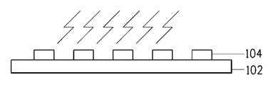
- 238000010304 firing Methods 0.000 claims description 19
- 239000002904 solvent Substances 0.000 claims description 9
- 238000001035 drying Methods 0.000 claims description 3
- 229910052796 boron Inorganic materials 0.000 description 29
- NIXOWILDQLNWCW-UHFFFAOYSA-M Acrylate Chemical compound [O-]C(=O)C=C NIXOWILDQLNWCW-UHFFFAOYSA-M 0.000 description 21
- 239000010949 copper Substances 0.000 description 20
- 229910052802 copper Inorganic materials 0.000 description 17
- 239000000203 mixture Substances 0.000 description 17
- 239000000758 substrate Substances 0.000 description 12
- 239000002491 polymer binding agent Substances 0.000 description 11
- 239000000523 sample Substances 0.000 description 11
- 239000003960 organic solvent Substances 0.000 description 10
- LYCAIKOWRPUZTN-UHFFFAOYSA-N Ethylene glycol Chemical compound OCCO LYCAIKOWRPUZTN-UHFFFAOYSA-N 0.000 description 9
- 230000003647 oxidation Effects 0.000 description 9
- 238000007254 oxidation reaction Methods 0.000 description 9
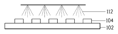
- 238000011161 development Methods 0.000 description 8
- 230000018109 developmental process Effects 0.000 description 8
- 229920000620 organic polymer Polymers 0.000 description 8
- 238000005245 sintering Methods 0.000 description 8
- BQCADISMDOOEFD-UHFFFAOYSA-N Silver Chemical compound [Ag] BQCADISMDOOEFD-UHFFFAOYSA-N 0.000 description 7
- 239000000843 powder Substances 0.000 description 7
- 229910052709 silver Inorganic materials 0.000 description 7
- 239000004332 silver Substances 0.000 description 7
- PEDCQBHIVMGVHV-UHFFFAOYSA-N Glycerine Chemical compound OCC(O)CO PEDCQBHIVMGVHV-UHFFFAOYSA-N 0.000 description 6
- 239000012298 atmosphere Substances 0.000 description 5
- 239000011230 binding agent Substances 0.000 description 5
- 238000000576 coating method Methods 0.000 description 5
- 150000001875 compounds Chemical class 0.000 description 5
- 239000000243 solution Substances 0.000 description 5
- DAFHKNAQFPVRKR-UHFFFAOYSA-N (3-hydroxy-2,2,4-trimethylpentyl) 2-methylpropanoate Chemical compound CC(C)C(O)C(C)(C)COC(=O)C(C)C DAFHKNAQFPVRKR-UHFFFAOYSA-N 0.000 description 4
- RTZKZFJDLAIYFH-UHFFFAOYSA-N Diethyl ether Chemical compound CCOCC RTZKZFJDLAIYFH-UHFFFAOYSA-N 0.000 description 4
- OFOBLEOULBTSOW-UHFFFAOYSA-N Malonic acid Chemical compound OC(=O)CC(O)=O OFOBLEOULBTSOW-UHFFFAOYSA-N 0.000 description 4
- KDLHZDBZIXYQEI-UHFFFAOYSA-N Palladium Chemical compound [Pd] KDLHZDBZIXYQEI-UHFFFAOYSA-N 0.000 description 4
- CDBYLPFSWZWCQE-UHFFFAOYSA-L Sodium Carbonate Chemical compound [Na+].[Na+].[O-]C([O-])=O CDBYLPFSWZWCQE-UHFFFAOYSA-L 0.000 description 4
- 230000015572 biosynthetic process Effects 0.000 description 4
- 239000004615 ingredient Substances 0.000 description 4
- 239000000463 material Substances 0.000 description 4
- 239000010970 precious metal Substances 0.000 description 4
- 238000007650 screen-printing Methods 0.000 description 4
- 238000012360 testing method Methods 0.000 description 4
- 239000012670 alkaline solution Substances 0.000 description 3
- 239000011248 coating agent Substances 0.000 description 3
- MTHSVFCYNBDYFN-UHFFFAOYSA-N diethylene glycol Chemical compound OCCOCCO MTHSVFCYNBDYFN-UHFFFAOYSA-N 0.000 description 3
- 239000006185 dispersion Substances 0.000 description 3
- 150000002148 esters Chemical class 0.000 description 3
- 238000005259 measurement Methods 0.000 description 3
- 229910052751 metal Inorganic materials 0.000 description 3
- 239000002184 metal Substances 0.000 description 3
- 238000002156 mixing Methods 0.000 description 3
- 239000011368 organic material Substances 0.000 description 3
- FZUGPQWGEGAKET-UHFFFAOYSA-N parbenate Chemical compound CCOC(=O)C1=CC=C(N(C)C)C=C1 FZUGPQWGEGAKET-UHFFFAOYSA-N 0.000 description 3
- 238000002360 preparation method Methods 0.000 description 3
- 239000002994 raw material Substances 0.000 description 3
- 239000007787 solid Substances 0.000 description 3
- 239000003381 stabilizer Substances 0.000 description 3
- GJZFGDYLJLCGHT-UHFFFAOYSA-N 1,2-diethylthioxanthen-9-one Chemical compound C1=CC=C2C(=O)C3=C(CC)C(CC)=CC=C3SC2=C1 GJZFGDYLJLCGHT-UHFFFAOYSA-N 0.000 description 2
- FRASJONUBLZVQX-UHFFFAOYSA-N 1,4-naphthoquinone Chemical compound C1=CC=C2C(=O)C=CC(=O)C2=C1 FRASJONUBLZVQX-UHFFFAOYSA-N 0.000 description 2
- RBGUKBSLNOTVCD-UHFFFAOYSA-N 1-methylanthracene-9,10-dione Chemical compound O=C1C2=CC=CC=C2C(=O)C2=C1C=CC=C2C RBGUKBSLNOTVCD-UHFFFAOYSA-N 0.000 description 2
- INQDDHNZXOAFFD-UHFFFAOYSA-N 2-[2-(2-prop-2-enoyloxyethoxy)ethoxy]ethyl prop-2-enoate Chemical compound C=CC(=O)OCCOCCOCCOC(=O)C=C INQDDHNZXOAFFD-UHFFFAOYSA-N 0.000 description 2
- FDSUVTROAWLVJA-UHFFFAOYSA-N 2-[[3-hydroxy-2,2-bis(hydroxymethyl)propoxy]methyl]-2-(hydroxymethyl)propane-1,3-diol;prop-2-enoic acid Chemical compound OC(=O)C=C.OC(=O)C=C.OC(=O)C=C.OC(=O)C=C.OC(=O)C=C.OCC(CO)(CO)COCC(CO)(CO)CO FDSUVTROAWLVJA-UHFFFAOYSA-N 0.000 description 2
- NJWGQARXZDRHCD-UHFFFAOYSA-N 2-methylanthraquinone Chemical compound C1=CC=C2C(=O)C3=CC(C)=CC=C3C(=O)C2=C1 NJWGQARXZDRHCD-UHFFFAOYSA-N 0.000 description 2
- 229930185605 Bisphenol Natural products 0.000 description 2
- VZCYOOQTPOCHFL-OWOJBTEDSA-N Fumaric acid Chemical compound OC(=O)\C=C\C(O)=O VZCYOOQTPOCHFL-OWOJBTEDSA-N 0.000 description 2
- MJVAVZPDRWSRRC-UHFFFAOYSA-N Menadione Chemical compound C1=CC=C2C(=O)C(C)=CC(=O)C2=C1 MJVAVZPDRWSRRC-UHFFFAOYSA-N 0.000 description 2
- -1 N, N-dimethylaminoethyl Chemical group 0.000 description 2
- PPBRXRYQALVLMV-UHFFFAOYSA-N Styrene Chemical compound C=CC1=CC=CC=C1 PPBRXRYQALVLMV-UHFFFAOYSA-N 0.000 description 2
- ZJCCRDAZUWHFQH-UHFFFAOYSA-N Trimethylolpropane Chemical compound CCC(CO)(CO)CO ZJCCRDAZUWHFQH-UHFFFAOYSA-N 0.000 description 2
- XSQUKJJJFZCRTK-UHFFFAOYSA-N Urea Chemical compound NC(N)=O XSQUKJJJFZCRTK-UHFFFAOYSA-N 0.000 description 2
- 230000002378 acidificating effect Effects 0.000 description 2
- 229910052797 bismuth Inorganic materials 0.000 description 2
- JCXGWMGPZLAOME-UHFFFAOYSA-N bismuth atom Chemical compound [Bi] JCXGWMGPZLAOME-UHFFFAOYSA-N 0.000 description 2
- IISBACLAFKSPIT-UHFFFAOYSA-N bisphenol A Chemical compound C=1C=C(O)C=CC=1C(C)(C)C1=CC=C(O)C=C1 IISBACLAFKSPIT-UHFFFAOYSA-N 0.000 description 2
- WERYXYBDKMZEQL-UHFFFAOYSA-N butane-1,4-diol Chemical compound OCCCCO WERYXYBDKMZEQL-UHFFFAOYSA-N 0.000 description 2
- 239000004202 carbamide Substances 0.000 description 2
- 239000003795 chemical substances by application Substances 0.000 description 2
- 230000000052 comparative effect Effects 0.000 description 2
- 238000011109 contamination Methods 0.000 description 2
- 238000010586 diagram Methods 0.000 description 2
- 238000009826 distribution Methods 0.000 description 2
- 239000000428 dust Substances 0.000 description 2
- 230000000694 effects Effects 0.000 description 2
- 238000005516 engineering process Methods 0.000 description 2
- PCHJSUWPFVWCPO-UHFFFAOYSA-N gold Chemical compound [Au] PCHJSUWPFVWCPO-UHFFFAOYSA-N 0.000 description 2
- 229910052737 gold Inorganic materials 0.000 description 2
- 239000010931 gold Substances 0.000 description 2
- 238000002844 melting Methods 0.000 description 2
- 230000008018 melting Effects 0.000 description 2
- 150000002739 metals Chemical class 0.000 description 2
- 229910052763 palladium Inorganic materials 0.000 description 2
- 238000000059 patterning Methods 0.000 description 2
- 229920000058 polyacrylate Polymers 0.000 description 2
- 229920000642 polymer Polymers 0.000 description 2
- 150000004053 quinones Chemical class 0.000 description 2
- 230000005855 radiation Effects 0.000 description 2
- 230000007261 regionalization Effects 0.000 description 2
- 229910000029 sodium carbonate Inorganic materials 0.000 description 2
- WUOACPNHFRMFPN-SECBINFHSA-N (S)-(-)-alpha-terpineol Chemical compound CC1=CC[C@@H](C(C)(C)O)CC1 WUOACPNHFRMFPN-SECBINFHSA-N 0.000 description 1
- RUJPNZNXGCHGID-UHFFFAOYSA-N (Z)-beta-Terpineol Natural products CC(=C)C1CCC(C)(O)CC1 RUJPNZNXGCHGID-UHFFFAOYSA-N 0.000 description 1
- NNNLYDWXTKOQQX-UHFFFAOYSA-N 1,1-di(prop-2-enoyloxy)propyl prop-2-enoate Chemical compound C=CC(=O)OC(CC)(OC(=O)C=C)OC(=O)C=C NNNLYDWXTKOQQX-UHFFFAOYSA-N 0.000 description 1
- AZESNEXPGASJRZ-UHFFFAOYSA-N 1,2,3,4-tetrahydrobenzo[a]anthracene-7,12-dione Chemical compound C1CCCC2=CC=C3C(=O)C4=CC=CC=C4C(=O)C3=C21 AZESNEXPGASJRZ-UHFFFAOYSA-N 0.000 description 1
- CWABICBDFJMISP-UHFFFAOYSA-N 1,3,5-tris(prop-1-en-2-yl)benzene Chemical compound CC(=C)C1=CC(C(C)=C)=CC(C(C)=C)=C1 CWABICBDFJMISP-UHFFFAOYSA-N 0.000 description 1
- ZENYUPUKNXGVDY-UHFFFAOYSA-N 1,4-bis(prop-1-en-2-yl)benzene Chemical compound CC(=C)C1=CC=C(C(C)=C)C=C1 ZENYUPUKNXGVDY-UHFFFAOYSA-N 0.000 description 1
- DVFAVJDEPNXAME-UHFFFAOYSA-N 1,4-dimethylanthracene-9,10-dione Chemical compound O=C1C2=CC=CC=C2C(=O)C2=C1C(C)=CC=C2C DVFAVJDEPNXAME-UHFFFAOYSA-N 0.000 description 1
- WVOVXOXRXQFTAS-UHFFFAOYSA-N 1-methyl-7-propan-2-ylphenanthrene-9,10-dione Chemical compound C1=CC=C2C3=CC=C(C(C)C)C=C3C(=O)C(=O)C2=C1C WVOVXOXRXQFTAS-UHFFFAOYSA-N 0.000 description 1
- GFVIWJYGBAXJAW-UHFFFAOYSA-N 2,2,5-trimethyl-3,4-diazabicyclo[3.2.2]nona-1(7),3-diene Chemical compound C1CC2=CCC1(C)N=NC2(C)C GFVIWJYGBAXJAW-UHFFFAOYSA-N 0.000 description 1
- KIJPZYXCIHZVGP-UHFFFAOYSA-N 2,3-dimethylanthracene-9,10-dione Chemical compound O=C1C2=CC=CC=C2C(=O)C2=C1C=C(C)C(C)=C2 KIJPZYXCIHZVGP-UHFFFAOYSA-N 0.000 description 1
- LZWVPGJPVCYAOC-UHFFFAOYSA-N 2,3-diphenylanthracene-9,10-dione Chemical compound C=1C=CC=CC=1C=1C=C2C(=O)C3=CC=CC=C3C(=O)C2=CC=1C1=CC=CC=C1 LZWVPGJPVCYAOC-UHFFFAOYSA-N 0.000 description 1
- OAYXUHPQHDHDDZ-UHFFFAOYSA-N 2-(2-butoxyethoxy)ethanol Chemical compound CCCCOCCOCCO OAYXUHPQHDHDDZ-UHFFFAOYSA-N 0.000 description 1
- VXQBJTKSVGFQOL-UHFFFAOYSA-N 2-(2-butoxyethoxy)ethyl acetate Chemical compound CCCCOCCOCCOC(C)=O VXQBJTKSVGFQOL-UHFFFAOYSA-N 0.000 description 1
- FPZWZCWUIYYYBU-UHFFFAOYSA-N 2-(2-ethoxyethoxy)ethyl acetate Chemical compound CCOCCOCCOC(C)=O FPZWZCWUIYYYBU-UHFFFAOYSA-N 0.000 description 1
- LCZVSXRMYJUNFX-UHFFFAOYSA-N 2-[2-(2-hydroxypropoxy)propoxy]propan-1-ol Chemical compound CC(O)COC(C)COC(C)CO LCZVSXRMYJUNFX-UHFFFAOYSA-N 0.000 description 1
- HWSSEYVMGDIFMH-UHFFFAOYSA-N 2-[2-[2-(2-methylprop-2-enoyloxy)ethoxy]ethoxy]ethyl 2-methylprop-2-enoate Chemical compound CC(=C)C(=O)OCCOCCOCCOC(=O)C(C)=C HWSSEYVMGDIFMH-UHFFFAOYSA-N 0.000 description 1
- TXBCBTDQIULDIA-UHFFFAOYSA-N 2-[[3-hydroxy-2,2-bis(hydroxymethyl)propoxy]methyl]-2-(hydroxymethyl)propane-1,3-diol Chemical compound OCC(CO)(CO)COCC(CO)(CO)CO TXBCBTDQIULDIA-UHFFFAOYSA-N 0.000 description 1
- POAOYUHQDCAZBD-UHFFFAOYSA-N 2-butoxyethanol Chemical compound CCCCOCCO POAOYUHQDCAZBD-UHFFFAOYSA-N 0.000 description 1
- NQBXSWAWVZHKBZ-UHFFFAOYSA-N 2-butoxyethyl acetate Chemical compound CCCCOCCOC(C)=O NQBXSWAWVZHKBZ-UHFFFAOYSA-N 0.000 description 1
- SJEBAWHUJDUKQK-UHFFFAOYSA-N 2-ethylanthraquinone Chemical compound C1=CC=C2C(=O)C3=CC(CC)=CC=C3C(=O)C2=C1 SJEBAWHUJDUKQK-UHFFFAOYSA-N 0.000 description 1
- LWRBVKNFOYUCNP-UHFFFAOYSA-N 2-methyl-1-(4-methylsulfanylphenyl)-2-morpholin-4-ylpropan-1-one Chemical compound C1=CC(SC)=CC=C1C(=O)C(C)(C)N1CCOCC1 LWRBVKNFOYUCNP-UHFFFAOYSA-N 0.000 description 1
- NTZCFGZBDDCNHI-UHFFFAOYSA-N 2-phenylanthracene-9,10-dione Chemical compound C=1C=C2C(=O)C3=CC=CC=C3C(=O)C2=CC=1C1=CC=CC=C1 NTZCFGZBDDCNHI-UHFFFAOYSA-N 0.000 description 1
- YTPSFXZMJKMUJE-UHFFFAOYSA-N 2-tert-butylanthracene-9,10-dione Chemical compound C1=CC=C2C(=O)C3=CC(C(C)(C)C)=CC=C3C(=O)C2=C1 YTPSFXZMJKMUJE-UHFFFAOYSA-N 0.000 description 1
- XFOHBSLKSOSFBE-UHFFFAOYSA-N 7,8,9,10-tetrahydrotetracene-5,12-dione Chemical compound C1CCCC2=C1C=C1C(=O)C3=CC=CC=C3C(=O)C1=C2 XFOHBSLKSOSFBE-UHFFFAOYSA-N 0.000 description 1
- RZVHIXYEVGDQDX-UHFFFAOYSA-N 9,10-anthraquinone Chemical compound C1=CC=C2C(=O)C3=CC=CC=C3C(=O)C2=C1 RZVHIXYEVGDQDX-UHFFFAOYSA-N 0.000 description 1
- 229940076442 9,10-anthraquinone Drugs 0.000 description 1
- YYVYAPXYZVYDHN-UHFFFAOYSA-N 9,10-phenanthroquinone Chemical compound C1=CC=C2C(=O)C(=O)C3=CC=CC=C3C2=C1 YYVYAPXYZVYDHN-UHFFFAOYSA-N 0.000 description 1
- ALQSHHUCVQOPAS-UHFFFAOYSA-N Pentane-1,5-diol Chemical compound OCCCCCO ALQSHHUCVQOPAS-UHFFFAOYSA-N 0.000 description 1
- OAICVXFJPJFONN-UHFFFAOYSA-N Phosphorus Chemical compound [P] OAICVXFJPJFONN-UHFFFAOYSA-N 0.000 description 1
- XBDQKXXYIPTUBI-UHFFFAOYSA-N Propionic acid Chemical class CCC(O)=O XBDQKXXYIPTUBI-UHFFFAOYSA-N 0.000 description 1
- 241000779819 Syncarpia glomulifera Species 0.000 description 1
- MDMKOESKPAVFJF-UHFFFAOYSA-N [4-(2-methylprop-2-enoyloxy)phenyl] 2-methylprop-2-enoate Chemical compound CC(=C)C(=O)OC1=CC=C(OC(=O)C(C)=C)C=C1 MDMKOESKPAVFJF-UHFFFAOYSA-N 0.000 description 1
- 150000001242 acetic acid derivatives Chemical class 0.000 description 1
- 150000001252 acrylic acid derivatives Chemical class 0.000 description 1
- NIXOWILDQLNWCW-UHFFFAOYSA-N acrylic acid group Chemical group C(C=C)(=O)O NIXOWILDQLNWCW-UHFFFAOYSA-N 0.000 description 1
- 230000002411 adverse Effects 0.000 description 1
- 150000001298 alcohols Chemical class 0.000 description 1
- 239000003513 alkali Substances 0.000 description 1
- OVKDFILSBMEKLT-UHFFFAOYSA-N alpha-Terpineol Natural products CC(=C)C1(O)CCC(C)=CC1 OVKDFILSBMEKLT-UHFFFAOYSA-N 0.000 description 1
- PYKYMHQGRFAEBM-UHFFFAOYSA-N anthraquinone Natural products CCC(=O)c1c(O)c2C(=O)C3C(C=CC=C3O)C(=O)c2cc1CC(=O)OC PYKYMHQGRFAEBM-UHFFFAOYSA-N 0.000 description 1
- 239000002518 antifoaming agent Substances 0.000 description 1
- LFYJSSARVMHQJB-QIXNEVBVSA-N bakuchiol Chemical compound CC(C)=CCC[C@@](C)(C=C)\C=C\C1=CC=C(O)C=C1 LFYJSSARVMHQJB-QIXNEVBVSA-N 0.000 description 1
- 239000011324 bead Substances 0.000 description 1
- LHMRXAIRPKSGDE-UHFFFAOYSA-N benzo[a]anthracene-7,12-dione Chemical compound C1=CC2=CC=CC=C2C2=C1C(=O)C1=CC=CC=C1C2=O LHMRXAIRPKSGDE-UHFFFAOYSA-N 0.000 description 1
- 238000007664 blowing Methods 0.000 description 1
- 238000009835 boiling Methods 0.000 description 1
- KGBXLFKZBHKPEV-UHFFFAOYSA-N boric acid Chemical compound OB(O)O KGBXLFKZBHKPEV-UHFFFAOYSA-N 0.000 description 1
- 239000004327 boric acid Substances 0.000 description 1
- 238000001354 calcination Methods 0.000 description 1
- 150000004649 carbonic acid derivatives Chemical class 0.000 description 1
- PMMYEEVYMWASQN-IMJSIDKUSA-N cis-4-Hydroxy-L-proline Chemical compound O[C@@H]1CN[C@H](C(O)=O)C1 PMMYEEVYMWASQN-IMJSIDKUSA-N 0.000 description 1
- 238000007796 conventional method Methods 0.000 description 1
- 238000001816 cooling Methods 0.000 description 1
- 229920001577 copolymer Polymers 0.000 description 1
- 238000004132 cross linking Methods 0.000 description 1
- FOTKYAAJKYLFFN-UHFFFAOYSA-N decane-1,10-diol Chemical compound OCCCCCCCCCCO FOTKYAAJKYLFFN-UHFFFAOYSA-N 0.000 description 1
- 238000000354 decomposition reaction Methods 0.000 description 1
- 230000007423 decrease Effects 0.000 description 1
- 230000007547 defect Effects 0.000 description 1
- 230000003111 delayed effect Effects 0.000 description 1
- 238000013461 design Methods 0.000 description 1
- 230000006866 deterioration Effects 0.000 description 1
- 239000002270 dispersing agent Substances 0.000 description 1
- 238000009837 dry grinding Methods 0.000 description 1
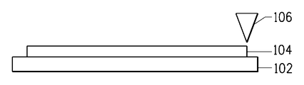
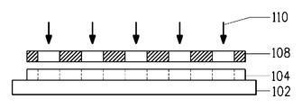
- 239000002003 electrode paste Substances 0.000 description 1
- 125000000816 ethylene group Chemical group [H]C([H])([*:1])C([H])([H])[*:2] 0.000 description 1
- 239000010419 fine particle Substances 0.000 description 1
- 239000001530 fumaric acid Substances 0.000 description 1
- PYGSKMBEVAICCR-UHFFFAOYSA-N hexa-1,5-diene Chemical group C=CCCC=C PYGSKMBEVAICCR-UHFFFAOYSA-N 0.000 description 1
- 125000004836 hexamethylene group Chemical group [H]C([H])([*:2])C([H])([H])C([H])([H])C([H])([H])C([H])([H])C([H])([H])[*:1] 0.000 description 1
- 239000003906 humectant Substances 0.000 description 1
- 150000004679 hydroxides Chemical class 0.000 description 1
- 239000012535 impurity Substances 0.000 description 1
- 238000007603 infrared drying Methods 0.000 description 1
- 229910010272 inorganic material Inorganic materials 0.000 description 1
- 239000011147 inorganic material Substances 0.000 description 1
- 125000005647 linker group Chemical group 0.000 description 1
- 150000002734 metacrylic acid derivatives Chemical class 0.000 description 1
- 239000012299 nitrogen atmosphere Substances 0.000 description 1
- 229910000510 noble metal Inorganic materials 0.000 description 1
- WXZMFSXDPGVJKK-UHFFFAOYSA-N pentaerythritol Chemical compound OCC(CO)(CO)CO WXZMFSXDPGVJKK-UHFFFAOYSA-N 0.000 description 1
- 229910052698 phosphorus Inorganic materials 0.000 description 1
- 239000011574 phosphorus Substances 0.000 description 1
- 239000001739 pinus spp. Substances 0.000 description 1
- 239000004014 plasticizer Substances 0.000 description 1
- 229920000120 polyethyl acrylate Polymers 0.000 description 1
- 229920005596 polymer binder Polymers 0.000 description 1
- 238000006116 polymerization reaction Methods 0.000 description 1
- 229920001296 polysiloxane Polymers 0.000 description 1
- 238000007639 printing Methods 0.000 description 1
- 238000010791 quenching Methods 0.000 description 1
- 230000000171 quenching effect Effects 0.000 description 1
- 150000003254 radicals Chemical class 0.000 description 1
- 239000004576 sand Substances 0.000 description 1
- 238000007789 sealing Methods 0.000 description 1
- 239000004065 semiconductor Substances 0.000 description 1
- 229920002545 silicone oil Polymers 0.000 description 1
- 239000007921 spray Substances 0.000 description 1
- 238000005507 spraying Methods 0.000 description 1
- 239000000126 substance Substances 0.000 description 1
- QJVXKWHHAMZTBY-GCPOEHJPSA-N syringin Chemical compound COC1=CC(\C=C\CO)=CC(OC)=C1O[C@H]1[C@H](O)[C@@H](O)[C@H](O)[C@@H](CO)O1 QJVXKWHHAMZTBY-GCPOEHJPSA-N 0.000 description 1
- 150000003505 terpenes Chemical class 0.000 description 1
- 235000007586 terpenes Nutrition 0.000 description 1
- 125000000999 tert-butyl group Chemical group [H]C([H])([H])C(*)(C([H])([H])[H])C([H])([H])[H] 0.000 description 1
- 125000000383 tetramethylene group Chemical group [H]C([H])([*:1])C([H])([H])C([H])([H])C([H])([H])[*:2] 0.000 description 1
- VZCYOOQTPOCHFL-UHFFFAOYSA-N trans-butenedioic acid Natural products OC(=O)C=CC(O)=O VZCYOOQTPOCHFL-UHFFFAOYSA-N 0.000 description 1
- 229940036248 turpentine Drugs 0.000 description 1
- XLYOFNOQVPJJNP-UHFFFAOYSA-N water Substances O XLYOFNOQVPJJNP-UHFFFAOYSA-N 0.000 description 1
- 238000001238 wet grinding Methods 0.000 description 1
Images

Classifications
-
- H—ELECTRICITY
- H01—ELECTRIC ELEMENTS
- H01B—CABLES; CONDUCTORS; INSULATORS; SELECTION OF MATERIALS FOR THEIR CONDUCTIVE, INSULATING OR DIELECTRIC PROPERTIES
- H01B1/00—Conductors or conductive bodies characterised by the conductive materials; Selection of materials as conductors
- H01B1/20—Conductive material dispersed in non-conductive organic material
- H01B1/22—Conductive material dispersed in non-conductive organic material the conductive material comprising metals or alloys
-
- H—ELECTRICITY
- H01—ELECTRIC ELEMENTS
- H01J—ELECTRIC DISCHARGE TUBES OR DISCHARGE LAMPS
- H01J1/00—Details of electrodes, of magnetic control means, of screens, or of the mounting or spacing thereof, common to two or more basic types of discharge tubes or lamps
- H01J1/02—Main electrodes
-
- G—PHYSICS
- G03—PHOTOGRAPHY; CINEMATOGRAPHY; ANALOGOUS TECHNIQUES USING WAVES OTHER THAN OPTICAL WAVES; ELECTROGRAPHY; HOLOGRAPHY
- G03F—PHOTOMECHANICAL PRODUCTION OF TEXTURED OR PATTERNED SURFACES, e.g. FOR PRINTING, FOR PROCESSING OF SEMICONDUCTOR DEVICES; MATERIALS THEREFOR; ORIGINALS THEREFOR; APPARATUS SPECIALLY ADAPTED THEREFOR
- G03F7/00—Photomechanical, e.g. photolithographic, production of textured or patterned surfaces, e.g. printing surfaces; Materials therefor, e.g. comprising photoresists; Apparatus specially adapted therefor
- G03F7/004—Photosensitive materials
- G03F7/0047—Photosensitive materials characterised by additives for obtaining a metallic or ceramic pattern, e.g. by firing
-
- H—ELECTRICITY
- H01—ELECTRIC ELEMENTS
- H01B—CABLES; CONDUCTORS; INSULATORS; SELECTION OF MATERIALS FOR THEIR CONDUCTIVE, INSULATING OR DIELECTRIC PROPERTIES
- H01B1/00—Conductors or conductive bodies characterised by the conductive materials; Selection of materials as conductors
- H01B1/14—Conductive material dispersed in non-conductive inorganic material
- H01B1/16—Conductive material dispersed in non-conductive inorganic material the conductive material comprising metals or alloys
-
- H—ELECTRICITY
- H01—ELECTRIC ELEMENTS
- H01J—ELECTRIC DISCHARGE TUBES OR DISCHARGE LAMPS
- H01J1/00—Details of electrodes, of magnetic control means, of screens, or of the mounting or spacing thereof, common to two or more basic types of discharge tubes or lamps
- H01J1/02—Main electrodes
- H01J1/13—Solid thermionic cathodes
- H01J1/14—Solid thermionic cathodes characterised by the material
-
- H—ELECTRICITY
- H01—ELECTRIC ELEMENTS
- H01J—ELECTRIC DISCHARGE TUBES OR DISCHARGE LAMPS
- H01J11/00—Gas-filled discharge tubes with alternating current induction of the discharge, e.g. alternating current plasma display panels [AC-PDP]; Gas-filled discharge tubes without any main electrode inside the vessel; Gas-filled discharge tubes with at least one main electrode outside the vessel
- H01J11/20—Constructional details
- H01J11/22—Electrodes, e.g. special shape, material or configuration
-
- H—ELECTRICITY
- H01—ELECTRIC ELEMENTS
- H01J—ELECTRIC DISCHARGE TUBES OR DISCHARGE LAMPS
- H01J9/00—Apparatus or processes specially adapted for the manufacture, installation, removal, maintenance of electric discharge tubes, discharge lamps, or parts thereof; Recovery of material from discharge tubes or lamps
- H01J9/02—Manufacture of electrodes or electrode systems
-
- G—PHYSICS
- G03—PHOTOGRAPHY; CINEMATOGRAPHY; ANALOGOUS TECHNIQUES USING WAVES OTHER THAN OPTICAL WAVES; ELECTROGRAPHY; HOLOGRAPHY
- G03F—PHOTOMECHANICAL PRODUCTION OF TEXTURED OR PATTERNED SURFACES, e.g. FOR PRINTING, FOR PROCESSING OF SEMICONDUCTOR DEVICES; MATERIALS THEREFOR; ORIGINALS THEREFOR; APPARATUS SPECIALLY ADAPTED THEREFOR
- G03F7/00—Photomechanical, e.g. photolithographic, production of textured or patterned surfaces, e.g. printing surfaces; Materials therefor, e.g. comprising photoresists; Apparatus specially adapted therefor
- G03F7/004—Photosensitive materials
- G03F7/027—Non-macromolecular photopolymerisable compounds having carbon-to-carbon double bonds, e.g. ethylenic compounds
-
- H—ELECTRICITY
- H01—ELECTRIC ELEMENTS
- H01J—ELECTRIC DISCHARGE TUBES OR DISCHARGE LAMPS
- H01J2211/00—Plasma display panels with alternate current induction of the discharge, e.g. AC-PDPs
- H01J2211/20—Constructional details
- H01J2211/22—Electrodes
- H01J2211/225—Material of electrodes
-
- Y—GENERAL TAGGING OF NEW TECHNOLOGICAL DEVELOPMENTS; GENERAL TAGGING OF CROSS-SECTIONAL TECHNOLOGIES SPANNING OVER SEVERAL SECTIONS OF THE IPC; TECHNICAL SUBJECTS COVERED BY FORMER USPC CROSS-REFERENCE ART COLLECTIONS [XRACs] AND DIGESTS
- Y10—TECHNICAL SUBJECTS COVERED BY FORMER USPC
- Y10S—TECHNICAL SUBJECTS COVERED BY FORMER USPC CROSS-REFERENCE ART COLLECTIONS [XRACs] AND DIGESTS
- Y10S430/00—Radiation imagery chemistry: process, composition, or product thereof
- Y10S430/1053—Imaging affecting physical property or radiation sensitive material, or producing nonplanar or printing surface - process, composition, or product: radiation sensitive composition or product or process of making binder containing
- Y10S430/1055—Radiation sensitive composition or product or process of making
- Y10S430/106—Binder containing
-
- Y—GENERAL TAGGING OF NEW TECHNOLOGICAL DEVELOPMENTS; GENERAL TAGGING OF CROSS-SECTIONAL TECHNOLOGIES SPANNING OVER SEVERAL SECTIONS OF THE IPC; TECHNICAL SUBJECTS COVERED BY FORMER USPC CROSS-REFERENCE ART COLLECTIONS [XRACs] AND DIGESTS
- Y10—TECHNICAL SUBJECTS COVERED BY FORMER USPC
- Y10S—TECHNICAL SUBJECTS COVERED BY FORMER USPC CROSS-REFERENCE ART COLLECTIONS [XRACs] AND DIGESTS
- Y10S430/00—Radiation imagery chemistry: process, composition, or product thereof
- Y10S430/1053—Imaging affecting physical property or radiation sensitive material, or producing nonplanar or printing surface - process, composition, or product: radiation sensitive composition or product or process of making binder containing
- Y10S430/1055—Radiation sensitive composition or product or process of making
- Y10S430/114—Initiator containing
Landscapes
- Engineering & Computer Science (AREA)
- Chemical & Material Sciences (AREA)
- Physics & Mathematics (AREA)
- Materials Engineering (AREA)
- Plasma & Fusion (AREA)
- Ceramic Engineering (AREA)
- General Physics & Mathematics (AREA)
- Manufacturing & Machinery (AREA)
- Dispersion Chemistry (AREA)
- Inorganic Chemistry (AREA)
- Spectroscopy & Molecular Physics (AREA)
- Conductive Materials (AREA)
- Gas-Filled Discharge Tubes (AREA)
- Materials For Photolithography (AREA)
- Transforming Electric Information Into Light Information (AREA)
Applications Claiming Priority (2)
| Application Number | Priority Date | Filing Date | Title |
|---|---|---|---|
| US12/496,920 | 2009-07-02 | ||
| US12/496,920 US8129088B2 (en) | 2009-07-02 | 2009-07-02 | Electrode and method for manufacturing the same |
Publications (1)
| Publication Number | Publication Date |
|---|---|
| KR20120032551A true KR20120032551A (ko) | 2012-04-05 |
Family
ID=42537876
Family Applications (1)
| Application Number | Title | Priority Date | Filing Date |
|---|---|---|---|
| KR1020127002809A Ceased KR20120032551A (ko) | 2009-07-02 | 2010-07-01 | 전극 및 이의 제조 방법 |
Country Status (7)
| Country | Link |
|---|---|
| US (1) | US8129088B2 (cg-RX-API-DMAC7.html) |
| EP (1) | EP2449571A1 (cg-RX-API-DMAC7.html) |
| JP (1) | JP5654588B2 (cg-RX-API-DMAC7.html) |
| KR (1) | KR20120032551A (cg-RX-API-DMAC7.html) |
| CN (1) | CN102473563B (cg-RX-API-DMAC7.html) |
| TW (1) | TW201115593A (cg-RX-API-DMAC7.html) |
| WO (1) | WO2011002964A1 (cg-RX-API-DMAC7.html) |
Cited By (4)
| Publication number | Priority date | Publication date | Assignee | Title |
|---|---|---|---|---|
| WO2019074190A1 (ko) * | 2017-10-12 | 2019-04-18 | 전자부품연구원 | 전도성 페이스트 조성물, 이의 제조방법 및 이로부터 형성된 전극 |
| KR20190041141A (ko) * | 2017-10-12 | 2019-04-22 | 전자부품연구원 | 전도성 페이스트 조성물, 이의 제조방법 및 이로부터 형성된 전극 |
| KR20190041145A (ko) * | 2017-10-12 | 2019-04-22 | 전자부품연구원 | 전도성 페이스트 조성물, 이의 제조방법 및 이로부터 형성된 전극 |
| KR20230077363A (ko) * | 2021-11-25 | 2023-06-01 | 한국화학연구원 | 포지티브형 감광성 페이스트 조성물과, 이를 이용한 전도성 패턴이 마련된 전극 및 그 제조방법 |
Families Citing this family (17)
| Publication number | Priority date | Publication date | Assignee | Title |
|---|---|---|---|---|
| US20110083874A1 (en) * | 2009-10-09 | 2011-04-14 | E. I. Du Pont De Nemours And Company | Electrode and method for manufacturing the same |
| US8728355B2 (en) * | 2011-01-14 | 2014-05-20 | E. I. Du Pont De Nemours And Company | Electrode and method for manufacturing the same |
| US8709294B2 (en) * | 2011-01-28 | 2014-04-29 | E. I. Du Pont De Nemours And Company | Electrode and method for manufacturing the same |
| US8647815B1 (en) | 2012-07-26 | 2014-02-11 | E I Du Pont De Nemours And Company | Method of manufacturing copper electrode |
| WO2014125470A1 (en) | 2013-02-18 | 2014-08-21 | Orbotech Ltd. | Two-step, direct- write laser metallization |
| US10622244B2 (en) | 2013-02-18 | 2020-04-14 | Orbotech Ltd. | Pulsed-mode direct-write laser metallization |
| US10537027B2 (en) | 2013-08-02 | 2020-01-14 | Orbotech Ltd. | Method producing a conductive path on a substrate |
| US20150197645A1 (en) * | 2014-01-16 | 2015-07-16 | E I Du Pont De Nemours And Company | Method of manufacturing non-firing type electrode |
| CN106663493A (zh) * | 2014-08-28 | 2017-05-10 | E.I.内穆尔杜邦公司 | 含铜导电浆料和由含铜导电浆料制成的电极 |
| JP6408696B2 (ja) | 2014-08-28 | 2018-10-17 | イー・アイ・デュポン・ドウ・ヌムール・アンド・カンパニーE.I.Du Pont De Nemours And Company | 銅含有導電性ペースト、及び銅含有導電性ペーストから作製された電極 |
| CN106575537A (zh) | 2014-08-28 | 2017-04-19 | E.I.内穆尔杜邦公司 | 具有铜电极的太阳能电池 |
| WO2016063270A1 (en) | 2014-10-19 | 2016-04-28 | Orbotech Ltd. | Llift printing of conductive traces onto a semiconductor substrate |
| KR101972676B1 (ko) | 2014-11-10 | 2019-04-25 | 다이켄카가쿠 코교 가부시키가이샤 | 대기 분위기 소성용 도전성 페이스트 및 그 제조 방법 |
| US10633758B2 (en) | 2015-01-19 | 2020-04-28 | Orbotech Ltd. | Printing of three-dimensional metal structures with a sacrificial support |
| US9966480B2 (en) * | 2015-04-28 | 2018-05-08 | Samsung Sdi Co., Ltd. | Electrode composition, electrode manufactured using the same, and solar cell |
| WO2017085712A1 (en) | 2015-11-22 | 2017-05-26 | Orbotech Ltd | Control of surface properties of printed three-dimensional structures |
| TW201901887A (zh) | 2017-05-24 | 2019-01-01 | 以色列商奧寶科技股份有限公司 | 於未事先圖樣化基板上電器互連電路元件 |
Family Cites Families (30)
| Publication number | Priority date | Publication date | Assignee | Title |
|---|---|---|---|---|
| BE525225A (cg-RX-API-DMAC7.html) | 1951-08-20 | |||
| US2875047A (en) | 1955-01-19 | 1959-02-24 | Oster Gerald | Photopolymerization with the formation of coherent plastic masses |
| US2850445A (en) | 1955-01-19 | 1958-09-02 | Oster Gerald | Photopolymerization |
| US3074974A (en) | 1957-12-06 | 1963-01-22 | Monsanto Chemicals | Method for the preparation of diglycidyl ether of tetrachlorobisphenol-a |
| US3097097A (en) | 1959-02-12 | 1963-07-09 | Gisela K Oster | Photo degrading of gel systems and photographic production of reliefs therewith |
| NL254306A (cg-RX-API-DMAC7.html) | 1959-08-07 | |||
| GB1090142A (en) | 1965-02-26 | 1967-11-08 | Agfa Gevaert Nv | Photochemical insolubilisation of polymers |
| US3479185A (en) | 1965-06-03 | 1969-11-18 | Du Pont | Photopolymerizable compositions and layers containing 2,4,5-triphenylimidazoyl dimers |
| US3380381A (en) * | 1965-08-06 | 1968-04-30 | Western Printing Mach Co | Rotary press printing cylinder for clamping flexible plates |
| US3549367A (en) | 1968-05-24 | 1970-12-22 | Du Pont | Photopolymerizable compositions containing triarylimidazolyl dimers and p-aminophenyl ketones |
| US4122232A (en) * | 1975-04-21 | 1978-10-24 | Engelhard Minerals & Chemicals Corporation | Air firable base metal conductors |
| US4070517A (en) * | 1976-07-08 | 1978-01-24 | Beckman Instruments, Inc. | Low fired conductive compositions |
| US4162162A (en) | 1978-05-08 | 1979-07-24 | E. I. Du Pont De Nemours And Company | Derivatives of aryl ketones and p-dialkyl-aminoarylaldehydes as visible sensitizers of photopolymerizable compositions |
| JPS5874030A (ja) * | 1981-10-28 | 1983-05-04 | ティーディーケイ株式会社 | 電子部品、導電皮膜組成物及び製造方法 |
| US5047313A (en) * | 1989-08-21 | 1991-09-10 | E. I. Du Pont De Nemours And Company | Photosensitive semi-aqueous developable copper conductor composition |
| JP2841586B2 (ja) * | 1989-12-04 | 1998-12-24 | 大同特殊鋼株式会社 | 導電性ペースト |
| JPH06349316A (ja) * | 1993-06-11 | 1994-12-22 | Tdk Corp | 導電ペースト |
| JP3079930B2 (ja) * | 1995-01-23 | 2000-08-21 | 株式会社村田製作所 | 磁器コンデンサ |
| US5851732A (en) | 1997-03-06 | 1998-12-22 | E. I. Du Pont De Nemours And Company | Plasma display panel device fabrication utilizing black electrode between substrate and conductor electrode |
| JPH11242930A (ja) * | 1997-12-03 | 1999-09-07 | Toray Ind Inc | 電極の製造方法およびプラズマディスプレイパネル用部材の製造方法 |
| KR20050122498A (ko) * | 2004-06-24 | 2005-12-29 | 삼성에스디아이 주식회사 | 감광성 페이스트 조성물, 이를 이용하여 제조된 pdp전극, 및 이를 포함하는 pdp |
| JP2006030853A (ja) * | 2004-07-21 | 2006-02-02 | Taiyo Ink Mfg Ltd | 感光性ペースト及びそれを用いて形成した焼成物パターン |
| JP4760709B2 (ja) * | 2004-07-22 | 2011-08-31 | 東レ株式会社 | 感光性ペーストおよびディスプレイパネル用部材の製造方法 |
| US7135267B2 (en) * | 2004-08-06 | 2006-11-14 | E. I. Du Pont De Nemours And Company | Aqueous developable photoimageable compositions for use in photo-patterning methods |
| KR100658714B1 (ko) * | 2004-11-30 | 2006-12-15 | 삼성에스디아이 주식회사 | 감광성 조성물, 이를 포함하는 격벽 형성용 감광성페이스트 조성물, 및 이를 이용한 플라즈마 디스플레이패널용 격벽의 제조방법. |
| JP2007012371A (ja) * | 2005-06-29 | 2007-01-18 | E I Du Pont De Nemours & Co | 導電組成物およびプラズマディスプレイの背面基板の製造方法 |
| US7655864B2 (en) | 2006-07-13 | 2010-02-02 | E.I Du Pont De Nemours And Company | Photosensitive conductive paste for electrode formation and electrode |
| KR100829667B1 (ko) * | 2006-09-07 | 2008-05-16 | 엘지전자 주식회사 | 전극용 페이스트 조성물, 이를 이용하여 제조된 플라즈마디스플레이 패널의 상판구조 및 그 제조방법 |
| KR100852705B1 (ko) | 2006-09-15 | 2008-08-19 | 삼성에스디아이 주식회사 | 전극 형성용 조성물과 이로부터 제조되는 플라즈마디스플레이 패널 |
| US7887992B2 (en) * | 2008-12-23 | 2011-02-15 | E. I. Du Pont De Nemours And Company | Photosensitive paste and process for production of pattern using the same |
-
2009
- 2009-07-02 US US12/496,920 patent/US8129088B2/en active Active
-
2010
- 2010-07-01 EP EP10735368A patent/EP2449571A1/en not_active Withdrawn
- 2010-07-01 KR KR1020127002809A patent/KR20120032551A/ko not_active Ceased
- 2010-07-01 JP JP2012517905A patent/JP5654588B2/ja not_active Expired - Fee Related
- 2010-07-01 CN CN201080027528.8A patent/CN102473563B/zh active Active
- 2010-07-01 TW TW099121709A patent/TW201115593A/zh unknown
- 2010-07-01 WO PCT/US2010/040719 patent/WO2011002964A1/en not_active Ceased
Cited By (4)
| Publication number | Priority date | Publication date | Assignee | Title |
|---|---|---|---|---|
| WO2019074190A1 (ko) * | 2017-10-12 | 2019-04-18 | 전자부품연구원 | 전도성 페이스트 조성물, 이의 제조방법 및 이로부터 형성된 전극 |
| KR20190041141A (ko) * | 2017-10-12 | 2019-04-22 | 전자부품연구원 | 전도성 페이스트 조성물, 이의 제조방법 및 이로부터 형성된 전극 |
| KR20190041145A (ko) * | 2017-10-12 | 2019-04-22 | 전자부품연구원 | 전도성 페이스트 조성물, 이의 제조방법 및 이로부터 형성된 전극 |
| KR20230077363A (ko) * | 2021-11-25 | 2023-06-01 | 한국화학연구원 | 포지티브형 감광성 페이스트 조성물과, 이를 이용한 전도성 패턴이 마련된 전극 및 그 제조방법 |
Also Published As
| Publication number | Publication date |
|---|---|
| EP2449571A1 (en) | 2012-05-09 |
| CN102473563B (zh) | 2014-07-23 |
| CN102473563A (zh) | 2012-05-23 |
| JP5654588B2 (ja) | 2015-01-14 |
| US20110003246A1 (en) | 2011-01-06 |
| TW201115593A (en) | 2011-05-01 |
| JP2012532420A (ja) | 2012-12-13 |
| US8129088B2 (en) | 2012-03-06 |
| WO2011002964A1 (en) | 2011-01-06 |
Similar Documents
| Publication | Publication Date | Title |
|---|---|---|
| KR20120032551A (ko) | 전극 및 이의 제조 방법 | |
| US20120255765A1 (en) | Electrode and method for manufacturing the same | |
| JP5080743B2 (ja) | 黒色導電性厚膜組成物、黒色電極、およびこれらの形成方法 | |
| US20060071202A1 (en) | Photosensitive paste composition | |
| JP2009544116A (ja) | 電極形成用感光性導電性ペーストおよび電極 | |
| KR101100490B1 (ko) | 플라즈마 디스플레이 패널용 전극 페이스트 및 플라즈마 디스플레이 패널용 블랙 버스 전극 | |
| CN101031845B (zh) | 用在光图案化方法中的可水溶液显影的可光成像的组合物前体 | |
| DE60204711T2 (de) | Wässrig entwickelbare, lichtempfindliche dickschichtbildaufzeichnungszusammensetzungen zur herstellung von schwarzen elektroden | |
| US8728355B2 (en) | Electrode and method for manufacturing the same | |
| KR101195639B1 (ko) | 중합체 용액, 수성 현상가능한 후막 조성물, 이들의 제조 방법 및 그로부터 형성된 전극 | |
| CN101816047A (zh) | 黑色汇流电极用导电组合物以及等离子显示屏的前面板 | |
| KR100799062B1 (ko) | 전도성 조성물 및 플라즈마 디스플레이의 배면 기판의 제조방법 | |
| US8709294B2 (en) | Electrode and method for manufacturing the same | |
| JP5421391B2 (ja) | Pdpの前部電極 | |
| JP2014063705A (ja) | Pdpバス電極の製造方法 | |
| KR20060029546A (ko) | 감광성 페이스트 조성물, 이를 이용하여 제조된 pdp전극, 및 이를 포함하는 pdp | |
| KR20050078447A (ko) | 디스플레이 장치용 감광성 도전 조성물 |
Legal Events
| Date | Code | Title | Description |
|---|---|---|---|
| A201 | Request for examination | ||
| PA0105 | International application |
Patent event date: 20120201 Patent event code: PA01051R01D Comment text: International Patent Application |
|
| PA0201 | Request for examination | ||
| PG1501 | Laying open of application | ||
| E902 | Notification of reason for refusal | ||
| PE0902 | Notice of grounds for rejection |
Comment text: Notification of reason for refusal Patent event date: 20130415 Patent event code: PE09021S01D |
|
| E601 | Decision to refuse application | ||
| PE0601 | Decision on rejection of patent |
Patent event date: 20130905 Comment text: Decision to Refuse Application Patent event code: PE06012S01D Patent event date: 20130415 Comment text: Notification of reason for refusal Patent event code: PE06011S01I |