KR20120032551A - Electrode and method for manufacturing the same - Google Patents
Electrode and method for manufacturing the same Download PDFInfo
- Publication number
- KR20120032551A KR20120032551A KR1020127002809A KR20127002809A KR20120032551A KR 20120032551 A KR20120032551 A KR 20120032551A KR 1020127002809 A KR1020127002809 A KR 1020127002809A KR 20127002809 A KR20127002809 A KR 20127002809A KR 20120032551 A KR20120032551 A KR 20120032551A
- Authority
- KR
- South Korea
- Prior art keywords
- weight
- electrode
- photosensitive paste
- powder
- boron
- Prior art date
Links
Images

Classifications
-
- H—ELECTRICITY
- H01—ELECTRIC ELEMENTS
- H01B—CABLES; CONDUCTORS; INSULATORS; SELECTION OF MATERIALS FOR THEIR CONDUCTIVE, INSULATING OR DIELECTRIC PROPERTIES
- H01B1/00—Conductors or conductive bodies characterised by the conductive materials; Selection of materials as conductors
- H01B1/20—Conductive material dispersed in non-conductive organic material
- H01B1/22—Conductive material dispersed in non-conductive organic material the conductive material comprising metals or alloys
-
- H—ELECTRICITY
- H01—ELECTRIC ELEMENTS
- H01J—ELECTRIC DISCHARGE TUBES OR DISCHARGE LAMPS
- H01J1/00—Details of electrodes, of magnetic control means, of screens, or of the mounting or spacing thereof, common to two or more basic types of discharge tubes or lamps
- H01J1/02—Main electrodes
-
- G—PHYSICS
- G03—PHOTOGRAPHY; CINEMATOGRAPHY; ANALOGOUS TECHNIQUES USING WAVES OTHER THAN OPTICAL WAVES; ELECTROGRAPHY; HOLOGRAPHY
- G03F—PHOTOMECHANICAL PRODUCTION OF TEXTURED OR PATTERNED SURFACES, e.g. FOR PRINTING, FOR PROCESSING OF SEMICONDUCTOR DEVICES; MATERIALS THEREFOR; ORIGINALS THEREFOR; APPARATUS SPECIALLY ADAPTED THEREFOR
- G03F7/00—Photomechanical, e.g. photolithographic, production of textured or patterned surfaces, e.g. printing surfaces; Materials therefor, e.g. comprising photoresists; Apparatus specially adapted therefor
- G03F7/004—Photosensitive materials
- G03F7/0047—Photosensitive materials characterised by additives for obtaining a metallic or ceramic pattern, e.g. by firing
-
- H—ELECTRICITY
- H01—ELECTRIC ELEMENTS
- H01B—CABLES; CONDUCTORS; INSULATORS; SELECTION OF MATERIALS FOR THEIR CONDUCTIVE, INSULATING OR DIELECTRIC PROPERTIES
- H01B1/00—Conductors or conductive bodies characterised by the conductive materials; Selection of materials as conductors
- H01B1/14—Conductive material dispersed in non-conductive inorganic material
- H01B1/16—Conductive material dispersed in non-conductive inorganic material the conductive material comprising metals or alloys
-
- H—ELECTRICITY
- H01—ELECTRIC ELEMENTS
- H01J—ELECTRIC DISCHARGE TUBES OR DISCHARGE LAMPS
- H01J1/00—Details of electrodes, of magnetic control means, of screens, or of the mounting or spacing thereof, common to two or more basic types of discharge tubes or lamps
- H01J1/02—Main electrodes
- H01J1/13—Solid thermionic cathodes
- H01J1/14—Solid thermionic cathodes characterised by the material
-
- H—ELECTRICITY
- H01—ELECTRIC ELEMENTS
- H01J—ELECTRIC DISCHARGE TUBES OR DISCHARGE LAMPS
- H01J11/00—Gas-filled discharge tubes with alternating current induction of the discharge, e.g. alternating current plasma display panels [AC-PDP]; Gas-filled discharge tubes without any main electrode inside the vessel; Gas-filled discharge tubes with at least one main electrode outside the vessel
- H01J11/20—Constructional details
- H01J11/22—Electrodes, e.g. special shape, material or configuration
-
- H—ELECTRICITY
- H01—ELECTRIC ELEMENTS
- H01J—ELECTRIC DISCHARGE TUBES OR DISCHARGE LAMPS
- H01J9/00—Apparatus or processes specially adapted for the manufacture, installation, removal, maintenance of electric discharge tubes, discharge lamps, or parts thereof; Recovery of material from discharge tubes or lamps
- H01J9/02—Manufacture of electrodes or electrode systems
-
- G—PHYSICS
- G03—PHOTOGRAPHY; CINEMATOGRAPHY; ANALOGOUS TECHNIQUES USING WAVES OTHER THAN OPTICAL WAVES; ELECTROGRAPHY; HOLOGRAPHY
- G03F—PHOTOMECHANICAL PRODUCTION OF TEXTURED OR PATTERNED SURFACES, e.g. FOR PRINTING, FOR PROCESSING OF SEMICONDUCTOR DEVICES; MATERIALS THEREFOR; ORIGINALS THEREFOR; APPARATUS SPECIALLY ADAPTED THEREFOR
- G03F7/00—Photomechanical, e.g. photolithographic, production of textured or patterned surfaces, e.g. printing surfaces; Materials therefor, e.g. comprising photoresists; Apparatus specially adapted therefor
- G03F7/004—Photosensitive materials
- G03F7/027—Non-macromolecular photopolymerisable compounds having carbon-to-carbon double bonds, e.g. ethylenic compounds
-
- H—ELECTRICITY
- H01—ELECTRIC ELEMENTS
- H01J—ELECTRIC DISCHARGE TUBES OR DISCHARGE LAMPS
- H01J2211/00—Plasma display panels with alternate current induction of the discharge, e.g. AC-PDPs
- H01J2211/20—Constructional details
- H01J2211/22—Electrodes
- H01J2211/225—Material of electrodes
-
- Y—GENERAL TAGGING OF NEW TECHNOLOGICAL DEVELOPMENTS; GENERAL TAGGING OF CROSS-SECTIONAL TECHNOLOGIES SPANNING OVER SEVERAL SECTIONS OF THE IPC; TECHNICAL SUBJECTS COVERED BY FORMER USPC CROSS-REFERENCE ART COLLECTIONS [XRACs] AND DIGESTS
- Y10—TECHNICAL SUBJECTS COVERED BY FORMER USPC
- Y10S—TECHNICAL SUBJECTS COVERED BY FORMER USPC CROSS-REFERENCE ART COLLECTIONS [XRACs] AND DIGESTS
- Y10S430/00—Radiation imagery chemistry: process, composition, or product thereof
- Y10S430/1053—Imaging affecting physical property or radiation sensitive material, or producing nonplanar or printing surface - process, composition, or product: radiation sensitive composition or product or process of making binder containing
- Y10S430/1055—Radiation sensitive composition or product or process of making
- Y10S430/106—Binder containing
-
- Y—GENERAL TAGGING OF NEW TECHNOLOGICAL DEVELOPMENTS; GENERAL TAGGING OF CROSS-SECTIONAL TECHNOLOGIES SPANNING OVER SEVERAL SECTIONS OF THE IPC; TECHNICAL SUBJECTS COVERED BY FORMER USPC CROSS-REFERENCE ART COLLECTIONS [XRACs] AND DIGESTS
- Y10—TECHNICAL SUBJECTS COVERED BY FORMER USPC
- Y10S—TECHNICAL SUBJECTS COVERED BY FORMER USPC CROSS-REFERENCE ART COLLECTIONS [XRACs] AND DIGESTS
- Y10S430/00—Radiation imagery chemistry: process, composition, or product thereof
- Y10S430/1053—Imaging affecting physical property or radiation sensitive material, or producing nonplanar or printing surface - process, composition, or product: radiation sensitive composition or product or process of making binder containing
- Y10S430/1055—Radiation sensitive composition or product or process of making
- Y10S430/114—Initiator containing
Abstract
구리 분말, 붕소 분말, 및 유리 프릿을 함유하는 무기 성분과 광중합 개시제, 단량체, 및 유기 비히클을 함유하는 유기 성분을 가지며, 구리 분말의 평균 입자 크기는 2.5 ㎛ 이하이고, 붕소 분말의 함량은 구리 분말과 붕소 분말의 총량을 기준으로 8 내지 25 중량%인 감광성 페이스트를 공기 중에서 베이킹함으로써 낮은 저항의, 미세 전극이 형성된다.Copper powder, boron powder, and an inorganic component containing a glass frit and an organic component containing a photopolymerization initiator, a monomer, and an organic vehicle, wherein the average particle size of the copper powder is 2.5 µm or less, and the content of the boron powder is copper powder. A low resistance, fine electrode is formed by baking in the air a photosensitive paste of 8 to 25% by weight based on the total amount of and boron powder.

Description
본 발명은 전기 소자의 전극에 관한 것이며, 더욱 구체적으로는 전극에 포함되는 전도성 성분의 개선에 관한 것이다.The present invention relates to an electrode of an electrical device, and more particularly to an improvement in the conductive component contained in the electrode.
전극의 원재료로서 전도성 페이스트를 사용하는 방법이 널리 알려져 있다. 전극 패턴의 마이크로화는 전자 소자의 기능적 개선과 함께 진보해 왔으며, 감광성 페이스트가 전자 소자 위에 미세 라인을 형성하는 데 사용된다. 예를 들어, 미세 전극 패턴은 플라즈마 디스플레이 패널(PDP)의 해상도를 개선하는 데 사용된다.The method of using a conductive paste as a raw material of an electrode is widely known. Micronization of electrode patterns has advanced with functional improvements in electronic devices, and photosensitive pastes are used to form fine lines on the electronic devices. For example, the fine electrode pattern is used to improve the resolution of the plasma display panel (PDP).
감광성 페이스트의 조성물은 일반적으로 광중합 개시제, 전도성 성분, 유리 프릿, 유기 결합제, 및 용매에 더하여 단량체를 포함한다. 적용된 감광성 페이스트는 마스크를 통해 노광되고, 노광된 위치에서 단량체의 중합이 진행된다. 그 후에, 현상 및 소성이 수행되고, 그에 의해 전도성 성분 및 결합제로서의 유리로 이루어진 전극이 형성된다.The composition of the photosensitive paste generally includes monomers in addition to the photopolymerization initiator, the conductive component, the glass frit, the organic binder, and the solvent. The applied photosensitive paste is exposed through a mask, and polymerization of the monomer proceeds at the exposed position. Thereafter, development and firing are performed, thereby forming an electrode made of glass as the conductive component and the binder.
은이 전도성 성분으로서 일반적으로 사용된다(예를 들어, 미국 특허 제5047313호 및 미국 특허 출원 공개 제20050287472호). 금, 은, 및 팔라듐과 같은 귀금속은 공기 중에서 소성될 수 있기 때문에, 노(furnace)에 대한 자본 투자가 감소될 수 있다. 그러나, 귀금속은 고가이기 때문에 귀금속의 사용은 재료 비용의 급격한 상승을 가져온다.Silver is generally used as the conductive component (see, for example, US Pat. No. 5047313 and US Patent Application Publication No. 20050287472). Since precious metals such as gold, silver, and palladium can be calcined in air, capital investment in furnaces can be reduced. However, because precious metals are expensive, the use of precious metals leads to a sharp rise in material costs.
구리가 반도체 회로 등에서 전도성 성분으로서 널리 사용된다. 구리는 은보다 저가인 이점을 갖는다. 그러나, 구리는 쉽게 산화되기 때문에 공기 중에서 소성될 수 없고, 질소 대기 등에서의 소성이 요구되기 때문에 자본 투자를 증가시킨다.Copper is widely used as a conductive component in semiconductor circuits and the like. Copper has the advantage of being cheaper than silver. However, copper cannot be fired in air because it is easily oxidized, and increases capital investment because firing in a nitrogen atmosphere or the like is required.
비-감광성 페이스트에서, 금속 분말과 함께 붕소를 사용하는 방법이 쉽게 산화가능한 금속의 공기 소성을 가능하게 하는 기술로서 개시되어 있다(미국 특허 제4,122,232호). 미국 특허 제4,122,232호의 실시예에서는, 325 메시보다 미세한 구리 분말이 사용된다. 구리 분말의 평균 입자 크기가 구체적으로 기재되어 있지는 않지만, 325 메시를 사용하여 선별된 구리 분말의 평균 입자 크기는 일반적으로 40 내지 50 ㎛이다.In non-photosensitive pastes, a method of using boron in conjunction with metal powders is disclosed as a technique that allows air firing of easily oxidizable metals (US Pat. No. 4,122,232). In the example of US Pat. No. 4,122,232, copper powder finer than 325 mesh is used. Although the average particle size of the copper powder is not specifically described, the average particle size of the copper powder selected using the 325 mesh is generally 40-50 μm.
이러한 기술을 감광성 페이스트에 적용하는 경우, 다양한 기술적 장애가 생겼다. 더욱 구체적으로, 붕소는 광을 산란시키는데, 붕소가 감광성 페이스트에 첨가되는 경우, 노출된 광이 산란되고 그에 의해 패턴의 형상이 유해한 영향을 받기 때문에 문제가 있었다. 더욱이, 전도성 성분에서는 우수한 미세 라인 형태를 얻기 위해서 작은 입자 크기가 바람직하나, 전도성 성분의 입자 크기가 작은 경우, 그의 표면적이 증가하고 그 결과로 산화가 더욱 쉽게 진행된다. 산화의 진행을 억제하기 위해서는 첨가되는 붕소의 양을 증가시키는 것이 바람직하나, 다량의 붕소가 함유되는 경우, 붕소는 전도성이 불량하기 때문에 전극의 저항이 증가한다.When this technique is applied to the photosensitive paste, various technical obstacles have arisen. More specifically, boron scatters light, which is problematic when boron is added to the photosensitive paste because the exposed light is scattered and the shape of the pattern is thereby adversely affected. Moreover, in the conductive component a small particle size is preferred in order to obtain a good fine line shape, but when the particle size of the conductive component is small, its surface area increases and as a result, oxidation proceeds more easily. In order to suppress the progress of oxidation, it is preferable to increase the amount of boron added. However, when a large amount of boron is contained, the resistance of the electrode increases because boron is poor in conductivity.
따라서, 페이스트를 사용하여 전극을 형성하는 방법에 있어서, 다음 요건들을 충족시키는 기술의 개발이 필요하다: 1) 저가의 구리 분말의 사용이 가능함, 2) 소성이 공기 중에서 수행되는 것이 가능함, 3) 미세 패턴의 형성이 가능함, 및 4) 낮은 전극 저항이 가능함.Therefore, in a method of forming an electrode using a paste, it is necessary to develop a technique that satisfies the following requirements: 1) the use of inexpensive copper powder is possible, 2) the firing can be performed in air, 3) Fine patterns can be formed, and 4) low electrode resistance is possible.
(발명의 요약)SUMMARY OF THE INVENTION [
본 발명은 전도성 성분으로서 구리 분말을 함유하며 공기 중 소성에 의해 형성되고 낮은 저항을 갖는, 미세하게 패턴화된 전극을 제공한다.The present invention provides finely patterned electrodes containing copper powder as the conductive component and formed by firing in air and having low resistance.
배경기술에서 언급된 문제는 본 명세서에 상세히 설명된 것과 같이 성분들의 함량, 입자 크기 등을 제어함으로써 해결될 수 있다.The problem mentioned in the background can be solved by controlling the content of ingredients, particle size and the like as described in detail herein.
더욱 구체적으로, 본 발명은 구리 분말, 붕소 분말, 및 유리 프릿을 포함하는 무기 성분과, 광중합 개시제, 단량체, 및 유기 비히클을 포함하는 유기 성분을 가지며, 구리 분말의 평균 입자 크기는 2.5 ㎛ 이하이고, 붕소 분말의 함량은, 구리 분말과 붕소 분말의 총량을 기준으로 8 내지 25 중량%인 감광성 페이스트를 공기 중에서 소성하여 형성되는 전극이다.More specifically, the present invention has an inorganic component including a copper powder, a boron powder, and a glass frit, and an organic component including a photopolymerization initiator, a monomer, and an organic vehicle, wherein the average particle size of the copper powder is 2.5 μm or less. , The content of the boron powder is an electrode formed by firing in the air a photosensitive paste of 8 to 25% by weight based on the total amount of copper powder and boron powder.
또한 본 발명은 구리 분말, 붕소 분말, 및 유리 프릿을 함유하는 무기 성분과, 광중합 개시제, 단량체, 및 유기 비히클을 함유하는 유기 성분을 가지며, 구리 분말의 평균 입자 크기는 2.5 ㎛ 이하이고, 붕소 분말의 함량은, 구리 분말과 붕소 분말의 총량을 기준으로 8 내지 25 중량%인 감광성 페이스트를 적용하는 단계; 적용된 감광성 페이스트를 건조시키는 단계; 건조된 감광성 페이스트를 노광시키는 단계; 노광된 감광성 페이스트를 현상하는 단계; 및 현상된 감광성 페이스트를 소성하여 전극 패턴을 형성하는 단계를 포함하는, 플라즈마 디스플레이 패널용 전극의 제조 방법이다.The present invention also has an inorganic component containing copper powder, boron powder, and glass frit, and an organic component containing a photopolymerization initiator, a monomer, and an organic vehicle, wherein the average particle size of the copper powder is 2.5 μm or less, and the boron powder The content of the, based on the total amount of the copper powder and boron powder 8 to 25% by weight of applying a photosensitive paste; Drying the applied photosensitive paste; Exposing the dried photosensitive paste; Developing the exposed photosensitive paste; And calcining the developed photosensitive paste to form an electrode pattern.
본 발명은 저가의 전도성 성분을 사용하여 공기 소성에 의해서 낮은 저항의, 미세 패턴을 형성하는 것을 가능하게 한다. 본 발명은 전자 소자용 전극의 생산 비용을 감소시키는 데 기여할 것이다.The present invention makes it possible to form low resistance, fine patterns by air firing using low cost conductive components. The present invention will contribute to reducing the production cost of electrodes for electronic devices.
<도 1>
도 1은 감광성 페이스트를 사용하여 어드레스 전극을 제조하는 방법을 예시하는 개략도.
<도 2>
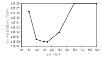
도 2는 붕소 함량과 표면 저항 사이의 관계를 나타내는 그래프.<Figure 1>
1 is a schematic diagram illustrating a method of manufacturing an address electrode using a photosensitive paste.
<FIG. 2>
2 is a graph showing the relationship between boron content and surface resistance.
본 발명을 예로서 플라즈마 디스플레이 패널(PDP)의 어드레스 전극에 대해 설명할 것이다. 본 발명을 PDP 어드레스 전극에 사용하는 것이 바람직하나, 본 발명의 용도가 이에 제한되지는 않는다.The address electrode of the plasma display panel PDP will be described as an example. Although the present invention is preferably used for the PDP address electrode, the use of the present invention is not limited thereto.
PDP 어드레스 전극은 감광성 페이스트를 사용하여 형성된다. 우선, 감광성 페이스트의 조성물을 설명할 것이다. 감광성 페이스트를 제형하기 위하여, 유기 요소와 필요할 수 있는 만큼의 용매를 사용하여 각각의 요소의 비히클을 제형하고, 그 다음 전도성 분말 및 유리 프릿과 혼합한다. 그 후에, 얻어진 혼합물을 샌드 믹서, 예를 들어, 롤 믹서, 믹서, 균질 믹서, 볼 밀 및 비드 밀을 사용하여 니딩(kneading)하고, 그에 의해 감광성 페이스트를 얻는다.The PDP address electrode is formed using the photosensitive paste. First, the composition of the photosensitive paste will be described. To formulate the photosensitive paste, the vehicle of each urea is formulated using the organic urea and as much solvent as necessary, and then mixed with the conductive powder and the glass frit. Thereafter, the obtained mixture is kneaded using a sand mixer, for example, a roll mixer, a mixer, a homogeneous mixer, a ball mill and a bead mill, thereby obtaining a photosensitive paste.
무기 성분Inorganic ingredients
구리 분말, 붕소 분말 및 유리 프릿이 전형적인 무기 성분이다.Copper powder, boron powder and glass frit are typical inorganic components.
(I) 구리 분말(I) copper powder
구리 분말은 전도성을 제공하기 위해 첨가된다. 구리 분말의 평균 직경은 2.5 ㎛ 미만, 바람직하게는 2.0 ㎛ 미만, 더욱 바람직하게는 1.5 ㎛ 미만이다. 직경의 하한은 특별히 제한되지 않으나, 재료 비용의 관점에서, 0.1 ㎛ 초과의 평균 직경을 갖는 구리 분말이 바람직하다.Copper powder is added to provide conductivity. The average diameter of the copper powder is less than 2.5 μm, preferably less than 2.0 μm, more preferably less than 1.5 μm. The lower limit of the diameter is not particularly limited, but from the viewpoint of material cost, copper powder having an average diameter of more than 0.1 mu m is preferred.
평균 직경은 레이저 회절 산란법을 사용해 입자 직경의 분포를 측정하여 얻으며, D50으로 정의될 수 있다. 마이크로택(Microtrac) 모델 X-100이 구매가능한 장치의 예이다.The average diameter is obtained by measuring the distribution of particle diameters using laser diffraction scattering and can be defined as D50. Microtrac Model X-100 is an example of a commercially available device.
미세한 입자 크기를 갖는 구리 분말을 사용하여 낮은 저항을 갖는 전극이 형성될 수 있다. 미세한 구리 분말을 사용하는 경우, 공기 소성이 수행될 때 산화가 진행되고, 그 결과로 전극의 저항이 증가하기 때문에 문제가 있었다. 미리 결정된 양의 붕소가 존재하는 조건 하에서 미세한 구리 분말을 사용함으로써 본 발명에서는 전극 저항이 감소된다.An electrode with low resistance can be formed using copper powder having a fine particle size. In the case of using fine copper powder, there is a problem because oxidation proceeds when air firing is performed, and as a result, the resistance of the electrode increases. The electrode resistance is reduced in the present invention by using fine copper powder under conditions in which a predetermined amount of boron is present.
구리의 형태는 특별히 한정되지 않는다. 구리는 구 또는 플레이크 형태일 수 있다. 그러나, 구 형태가 감광성 페이스트에서 바람직하다.The form of copper is not specifically limited. Copper may be in the form of spheres or flakes. However, spherical form is preferred in the photosensitive paste.
구리 분말의 함량은 감광성 페이스트의 총량을 기준으로 20 내지 65 중량%인 것이 바람직하다.The content of the copper powder is preferably 20 to 65% by weight based on the total amount of the photosensitive paste.
구리 분말 이외의 금속이 감광성 페이스트에 함유될 수 있으나, 원재료의 비용을 감소시키는 견지에서, 은, 금, 또는 팔라듐과 같은 귀금속은 사실상 그에 함유되지 않는다. 본 명세서에서, 용어 "사실상 함유되지 않는"은 귀금속이 의도치 않게 불순물로서 함유되는 경우를 포함하는 개념이다.Metals other than copper powder may be contained in the photosensitive paste, but in view of reducing the cost of raw materials, precious metals such as silver, gold, or palladium are virtually free of it. As used herein, the term "virtually free" is a concept including the case where a noble metal is unintentionally contained as an impurity.
(II) 붕소 분말(II) Boron Powder
붕소 분말은 소성 중에 구리의 산화를 방지하기 위해 사용된다. 구리의 산화로 인한 전극 저항의 증가는 페이스트에 붕소 분말을 첨가함으로써 억제될 수 있다.Boron powder is used to prevent oxidation of copper during firing. The increase in electrode resistance due to oxidation of copper can be suppressed by adding boron powder to the paste.
평균 입자 직경은 바람직하게는 3 ㎛, 더욱 바람직하게는 2 ㎛ 미만이다. 평균 직경은 레이저 회절 산란법을 사용해 입자 직경의 분포를 측정하여 얻으며, D50으로 정의될 수 있다. 마이크로택 모델 X-100이 구매가능한 장치의 예이다. 직경의 하한은 특별히 제한되지 않으나, 재료 비용의 관점에서, 0.1 ㎛ 초과의 평균 직경을 갖는 붕소 분말이 바람직하다.The average particle diameter is preferably 3 μm, more preferably less than 2 μm. The average diameter is obtained by measuring the distribution of particle diameters using laser diffraction scattering and can be defined as D50. Microtack Model X-100 is an example of a commercially available device. The lower limit of the diameter is not particularly limited, but from the viewpoint of material cost, boron powder having an average diameter of more than 0.1 mu m is preferred.
작은 입자 크기의 붕소 분말을 사용하는 것이 얇은 전극을 형성하는 경우에 효과적이다. 막 두께가 1 내지 4 ㎛인 얇은 전극을 형성하는 경우, 큰 입자 크기를 갖는 붕소 분말의 사용은 현상 시점에서 막 외관의 품질 저하를 야기한다. 상기에 명시된 작은 입자 크기를 갖는 붕소 분말을 사용함으로써 전극 외관이 우수하게 보존될 수 있다.Using boron powder of small particle size is effective in forming thin electrodes. In the case of forming a thin electrode having a film thickness of 1 to 4 mu m, the use of boron powder having a large particle size causes a deterioration in the quality of the film appearance at the time of development. By using boron powder having the small particle size specified above, the electrode appearance can be well preserved.
붕소 분말의 함량은 구리 분말과 붕소 분말의 총량을 기준으로 바람직하게는 8 내지 25 중량%, 더욱 바람직하게는 9 내지 22 중량%, 더 더욱 바람직하게는 10 내지 19 중량%, 그리고 가장 바람직하게는 14 내지 18 중량%이다. 붕소 함량이 너무 낮은 경우, 구리 분말의 산화가 충분히 억제되지 않고 전극의 저항이 증가한다. 붕소 함량이 너무 높은 경우, 전도성 성분의 함량이 감소하기 때문에 전극의 저항이 증가한다. 더욱이, 붕소 함량이 너무 높은 경우에는, 노광 효율이 떨어지고 전극의 형상이 일그러진다.The content of boron powder is preferably from 8 to 25% by weight, more preferably from 9 to 22% by weight, even more preferably from 10 to 19% by weight, and most preferably based on the total amount of copper powder and boron powder. 14 to 18 weight percent. If the boron content is too low, the oxidation of the copper powder is not sufficiently inhibited and the resistance of the electrode increases. If the boron content is too high, the resistance of the electrode increases because the content of the conductive component is reduced. Moreover, when the boron content is too high, the exposure efficiency is lowered and the shape of the electrode is distorted.
붕소 분말의 함량은 감광성 페이스트의 총량을 기준으로 2 내지 18 중량%인 것이 바람직하다.The content of boron powder is preferably 2 to 18% by weight based on the total amount of photosensitive paste.
(III) 유리 프릿(III) glass frit
유리 프릿은 조성물과 기재, 예를 들어, PDP의 후방 패널에 사용되는 유리 기재의 밀봉 특성을 증가시킬 수 있다.Glass frits can increase the sealing properties of compositions and substrates, such as glass substrates used in the back panel of a PDP.
유리 프릿의 유형에는 비스무트계 유리 프릿, 붕산계 유리 프릿, 인계 유리 프릿, Zn-B계 유리 프릿, 및 납계 유리 프릿이 포함된다. 환경에 가해지는 부담을 고려하여 무연(lead-free) 유리 프릿을 사용하는 것이 바람직하다.Types of glass frits include bismuth based glass frits, boric acid based glass frits, phosphorus based glass frits, Zn-B based glass frits, and lead based glass frits. It is preferable to use lead-free glass frits in consideration of the burden on the environment.
유리 프릿은 본 기술 분야에 잘 알려진 방법에 의해 제조될 수 있다. 예를 들어, 유리 성분은 산화물, 수산화물, 카르보네이트 등과 같은 원재료를 혼합하고 용융시키며 급냉에 의해 컬릿(cullet)으로 만든 다음 기계적 미분화(습식 또는 건식 밀링)에 의해 제조될 수 있다. 그 후에, 필요한 경우, 원하는 입자 크기로 분류가 수행된다.Glass frits can be prepared by methods well known in the art. For example, the glass component can be prepared by mixing and melting raw materials such as oxides, hydroxides, carbonates, etc., into cullets by quenching and then by mechanical micronization (wet or dry milling). Thereafter, if necessary, classification is carried out to the desired particle size.
유리 프릿의 연화점은 보통 325 내지 700℃, 바람직하게는 350 내지 650℃, 그리고 더 더욱 바람직하게는 550 내지 600℃이다. 325℃보다 낮은 온도에서 용융이 일어나는 경우, 유기 물질이 감싸여지는 경향이 있을 것이고, 유기 물질의 후속적인 분해는 페이스트 내에 블리스터(blister)가 생성되게 할 것이다. 한편, 700℃ 초과의 연화점은 페이스트 부착을 약화시킬 것이며 유리 기판에 손상을 입힐 수 있다.The softening point of the glass frit is usually 325 to 700 ° C, preferably 350 to 650 ° C, and even more preferably 550 to 600 ° C. If melting occurs at a temperature lower than 325 ° C., the organic material will tend to wrap, and subsequent decomposition of the organic material will result in blister formation in the paste. On the other hand, softening points above 700 ° C. will weaken the paste adhesion and may damage the glass substrate.
유리 프릿의 비표면적은 10 ㎡/g 이하인 것이 바람직하다. 평균 직경은 일반적으로 0.1 내지 10 ㎛이다. 유리 프릿의 90 중량% 이상이 0.4 내지 10 ㎛의 입자 직경을 갖는 것이 바람직하다.It is preferable that the specific surface area of a glass frit is 10 m <2> / g or less. The average diameter is generally 0.1 to 10 μm. It is preferred that at least 90% by weight of the glass frit have a particle diameter of 0.4 to 10 μm.
유리 프릿의 함량은, 감광성 페이스트의 총량을 기준으로 0.1 내지5 중량%인 것이 바람직하다. 이러한 범위 내의 유리 프릿의 비율은 인접한 구성요소들과의 접합을 보장할 것이며, 그에 의해 충분히 강한 버스 전극의 형성이 보장될 것이다.The content of the glass frit is preferably 0.1 to 5% by weight based on the total amount of the photosensitive paste. The proportion of glass frit within this range will ensure bonding with adjacent components, thereby ensuring the formation of sufficiently strong bus electrodes.
유기 성분Organic ingredients
광중합 개시제, 단량체, 유기 비히클이 전형적인 유기 성분이다. 보통, 유기 비히클은 유기 중합체 결합제 및 용매를 함유한다.Photopolymerization initiators, monomers, and organic vehicles are typical organic components. Usually, the organic vehicle contains an organic polymer binder and a solvent.
(I) 광중합 개시제(I) photopolymerization initiator
광중합 개시제는 광중합-유형 단량체를 광중합하는 데 사용된다. 광중합 개시제는 바람직하게는 185℃ 이하에서 열적으로 비활성이나, 화학방사선에 노출 시 자유 라디칼을 발생시킨다.Photopolymerization initiators are used to photopolymerize photopolymerization-type monomers. The photopolymerization initiator is preferably thermally inert below 185 ° C., but generates free radicals upon exposure to actinic radiation.
광중합 개시제의 예에는 공액 탄소환식 고리 시스템 내에 2개의 분자내 고리를 갖는 화합물이 포함된다. 이러한 유형의 화합물은 치환되거나 비치환된 다핵성 퀴논을 포함한다.Examples of photopolymerization initiators include compounds having two intramolecular rings in a conjugated carbocyclic ring system. Compounds of this type include substituted or unsubstituted polynuclear quinones.
실제적으로, 퀴논의 예에는 에틸 4-다이메틸 아미노벤조에이트, 다이에틸티옥산톤, 9,10-안트라퀴논, 2-메틸안트라퀴논, 2-에틸안트라퀴논, 2-t-부틸안트라퀴논, 옥타메틸안트라퀴논, 1,4-나프토퀴논, 9,10-페난트렌퀴논, 벤조[a]안트라센-7,12 다이온, 2,3-나프타센-5,12-다이온, 2-메틸-1,4-나프토퀴논, 1,4-다이메틸안트라퀴논, 2,3-다이메틸안트라퀴논, 2-페닐안트라퀴논, 2,3-다이페닐안트라퀴논, 레텐퀴논(retenequinone), 7,8,9,10-테트라하이드로나프타센-5,12-다이온 및 1,2,3,4-테트라하이드로벤조[a]안트라센-7,12-다이온이 포함된다.In practice, examples of quinones include ethyl 4-dimethyl aminobenzoate, diethyl thioxanthone, 9,10-anthraquinone, 2-methylanthraquinone, 2-ethylanthraquinone, 2-t-butylanthraquinone, octa Methylanthraquinone, 1,4-naphthoquinone, 9,10-phenanthrenequinone, benzo [a] anthracene-7,12 dione, 2,3-naphthacene-5,12-dione, 2-methyl- 1,4-naphthoquinone, 1,4-dimethylanthraquinone, 2,3-dimethylanthraquinone, 2-phenylanthraquinone, 2,3-diphenylanthraquinone, retenquinone, 7,8 , 9,10-tetrahydronaphthacene-5,12-dione and 1,2,3,4-tetrahydrobenzo [a] anthracene-7,12-dione.
사용될 수 있는 기타 화합물에는 미국 특허 제2,760,863호, 제2,850,445호, 제2,875,047호, 제3,074,974호, 제3,097,097호, 제3,145,104호, 제3,427,161호, 제3,479,185호, 제3,549,367호, 및 제4,162,162호에서 주어진 것들이 포함된다.Other compounds that may be used include US Pat. Nos. 2,760,863, 2,850,445, 2,875,047, 3,074,974, 3,097,097, 3,145,104, 3,427,161, 3,479,185, 3,549,367, and 4,162,162. Things are included.
광중합 개시제의 함량은 감광성 페이스트의 총량을 기준으로 0.1 내지 10 중량%인 것이 바람직하다.The content of the photopolymerization initiator is preferably 0.1 to 10% by weight based on the total amount of the photosensitive paste.
(II) 광중합 단량체(II) photopolymerization monomer
광중합성 단량체는 특별히 한정되지 않는다. 예에는, 적어도 하나의 중합성 에틸렌 기를 갖는 에틸렌계 불포화 화합물이 포함된다. 바람직하게는, 감광성 페이스트는 3개 이상의 연결 기를 갖는 적어도 하나의 다중점 가교결합 단량체를 함유한다.The photopolymerizable monomer is not particularly limited. Examples include ethylenically unsaturated compounds having at least one polymerizable ethylene group. Preferably, the photosensitive paste contains at least one multipoint crosslinking monomer having three or more linking groups.
바람직한 단량체의 예에는 (메타)아크릴산 t-부틸, 1,5-펜탄다이올다이(메타)아크릴레이트, (메타)아크릴산 N,N-다이메틸아미노에틸, 에틸렌글리콜다이(메타)아크릴레이트, 1,4-부탄다이올다이(메타)아크릴레이트, 다이에틸렌글리콜다이(메타)아크릴레이트, 헥사메틸렌글리콜다이(메타)아크릴레이트, 1,3-프로판다이올다이(메타)아크릴레이트, 데카메틸렌글리콜다이(메타)아크릴레이트, 1,4-사이클로헥산다이올다이(메타)아크릴레이트, 2,2-다이메틸올프로판다이(메타)아크릴레이트, 글리세롤다이(메타)아크릴레이트, 트라이프로필렌글리콜다이(메타)아크릴레이트, 글리세롤트라이(메타)아크릴레이트, 트라이메틸올프로판트라이(메타)아크릴레이트, 트라이메틸올프로판 에톡시트라이아크릴레이트, 미국 특허 제3,380,381호에 개시된 화합물, 2,2-다이(p-하이드록시페닐)-프로판다이(메타)아크릴레이트, 펜타에리트리톨테트라(메타)아크릴레이트, 다이펜타에리트리톨 펜타아크릴레이트, 다이펜타에리트리톨 테트라아크릴레이트, 트라이에틸렌글리콜다이아크릴레이트, 폴리옥시에틸-1,2-다이-(p-하이드록시에틸)프로판다이메타크릴레이트, 비스페놀A다이-[3-(메타)아크릴옥시-2-하이드록시프로필]에테르, 비스페놀A다이-[2-(메타)아크릴옥시에틸]에테르, 1,4-부탄다이올다이-(3-메타크릴옥시-2-하이드록시프로필)에테르, 트라이에틸렌글리콜다이메타크릴레이트, 폴리옥시프로필트라이메틸올프로판트라이아크릴레이트, 부틸렌글리콜다이(메타)아크릴레이트, 1,2,4-부탄다이올트라이(메타)아크릴레이트, 2,2,4-트라이메틸-1,3-펜탄다이올다이(메타)아크릴레이트, 1-페닐에틸렌-1,2-다이메타크릴레이트, 푸마르산 다이알릴(fumaric diallyl), 스티렌, 1,4-벤젠다이올다이메타크릴레이트, 1,4-다이아이소프로페닐벤젠 및 1,3,5-트라이아이소프로페닐벤젠이 포함된다. 여기서, (메타)아크릴레이트는 아크릴레이트와 메타크릴레이트 둘 모두를 나타낸다.Examples of preferred monomers include t-butyl (meth) acrylate, 1,5-pentanediol di (meth) acrylate, N, N-dimethylaminoethyl (meth) acrylate, ethylene glycol di (meth) acrylate, 1 , 4-butanediol di (meth) acrylate, diethylene glycol di (meth) acrylate, hexamethylene glycoldi (meth) acrylate, 1,3-propanedioldi (meth) acrylate, decamethylene glycol Di (meth) acrylate, 1,4-cyclohexanediol di (meth) acrylate, 2,2-dimethylolpropanedi (meth) acrylate, glycerol di (meth) acrylate, tripropylene glycol die ( Meth) acrylate, glycerol tri (meth) acrylate, trimethylolpropane tri (meth) acrylate, trimethylolpropane ethoxy triacrylate, compounds disclosed in US Pat. No. 3,380,381, 2,2-di (p -Hi Oxyphenyl) -propanedi (meth) acrylate, pentaerythritol tetra (meth) acrylate, dipentaerythritol pentaacrylate, dipentaerythritol tetraacrylate, triethylene glycol diacrylate, polyoxyethyl-1 , 2-di- (p-hydroxyethyl) propanedimethacrylate, bisphenol Adi- [3- (meth) acryloxy-2-hydroxypropyl] ether, bisphenol Adi- [2- (meth) acrylic Oxyethyl] ether, 1,4-butanedioldi- (3-methacryloxy-2-hydroxypropyl) ether, triethylene glycol dimethacrylate, polyoxypropyltrimethylol propane triacrylate, butylene Glycoldi (meth) acrylate, 1,2,4-butanediol tri (meth) acrylate, 2,2,4-trimethyl-1,3-pentanedioldi (meth) acrylate, 1-phenyl Ethylene-1,2-dimethacrylate, fumaric acid dial (Fumaric diallyl), styrene, include 1,4-benzene diol dimethacrylate, 1,4-diisopropenyl benzene and 1,3,5-tri-isopropenyl benzene. Here, (meth) acrylate refers to both acrylates and methacrylates.
바람직하게는, 단량체 함량은 무기 성분의 총량에 대해 8 내지 35 중량%이다. 단량체 함량이 너무 낮은 경우에는, 노광 효율이 떨어지고, 전극의 폭이 너무 좁아진다. 일부 경우에, 불량한 노광으로 인해 전극에서 단선 및 단락이 일어난다. 한편으로, 단량체 함량이 너무 높은 경우에는, 전극 저항이 증가하고 표면 끈적임(stickiness)이 증가한다.Preferably, the monomer content is 8 to 35% by weight relative to the total amount of the inorganic component. If the monomer content is too low, the exposure efficiency is lowered, and the width of the electrode becomes too narrow. In some cases, broken and short circuits occur at the electrodes due to poor exposure. On the other hand, when the monomer content is too high, the electrode resistance increases and the surface stickiness increases.
광중합 단량체의 함량은 감광성 페이스트의 총량을 기준으로 1 내지 24 중량%인 것이 바람직하다.The content of the photopolymerization monomer is preferably 1 to 24% by weight based on the total amount of the photosensitive paste.
(III) 유기 중합체 결합제(III) organic polymer binder
유기 결합제는 전도성 분말, 붕소 분말 및 유리 프릿과 같은 구성성분을 조성물 내에 분산시키는 데 사용된다. 유기 중합체 결합제는 공지의 방법을 사용하여 스크린 인쇄 또는 관련 기술에서 기재 상에 전도성 페이스트를 코팅할 때 코팅 특성 및 코팅막의 안정성을 개선하는 데 사용된다. 유기 중합체 결합제는 감광성 페이스트를 소결하여 전극이 형성될 때 제거된다.Organic binders are used to disperse components such as conductive powders, boron powders and glass frits in the composition. Organic polymer binders are used to improve coating properties and stability of coatings when coating conductive paste on substrates in screen printing or related art using known methods. The organic polymer binder is removed when the electrode is formed by sintering the photosensitive paste.
코팅되고 건조된 감광성 페이스트를 수성 현상액을 사용하여 현상하고 그의 패턴을 형성할 때, 수성 현상액을 사용하는 현상 능력을 고려하여 고도의 분해능을 갖는 유기 중합체 결합제를 사용하는 것이 바람직하다. 이러한 조건을 충족시킬 수 있는 유기 중합체 결합제의 예에는 비-산성 공단량체 또는 산성 공단량체를 함유하는 것이 포함된다. 공중합체 또는 혼성중합체(interpolymer)(혼합된 중합체)가 또한 바람직하다. 유기 중합체 결합제의 다른 예는 아크릴 중합체 결합제 또는 미국 특허 출원 공개 제2007-0001607호에 나타나있는 기타 중합체 결합제이다.When developing the coated and dried photosensitive paste using an aqueous developer and forming a pattern thereof, it is preferable to use an organic polymer binder having a high resolution in consideration of the developing ability using the aqueous developer. Examples of organic polymer binders capable of meeting these conditions include those containing non-acidic comonomers or acidic comonomers. Copolymers or interpolymers (mixed polymers) are also preferred. Other examples of organic polymer binders are acrylic polymer binders or other polymer binders shown in US Patent Application Publication No. 2007-0001607.
유기 중합체 결합제의 함량은 감광성 페이스트의 총량을 기준으로 2 내지 30 중량%인 것이 바람직하다.The content of the organic polymer binder is preferably 2 to 30% by weight based on the total amount of the photosensitive paste.
(IV) 용매(IV) solvent
유기 용매를 사용하는 주요 목적은 조성물에 함유된 고형물의 분산물이 기판에 용이하게 적용되게 하는 것이다. 이와 같이, 유기 용매는 무엇보다도 고형물이 분산되게 하면서 적합한 안정성을 유지하는 것이 바람직하다. 두 번째로, 분산물에 유리한 적용 특성을 주기 위해 유기 용매의 유동학적 특성이 바람직하다.The main purpose of using organic solvents is to make the dispersion of the solids contained in the composition easily applied to the substrate. As such, it is desirable that the organic solvent, among other things, maintain suitable stability while allowing the solids to be dispersed. Secondly, the rheological properties of the organic solvent are preferred to give advantageous application properties to the dispersion.
유기 용매는 단일 성분이거나 또는 유기 용매들의 혼합물일 수 있다. 선택되는 유기 용매는 중합체 및 기타 유기 성분들이 완전히 용해될 수 있는 것이 바람직하다. 선택되는 유기 용매는 조성물 중의 다른 성분들에 대하여 비활성인 것이 바람직하다. 유기 용매는 충분히 높은 휘발성을 갖는 것이 바람직하며, 대기 내에서 비교적 낮은 온도에서 적용될 때에도 분산물로부터 증발 제거될 수 있는 것이 바람직하다. 용매는 인쇄 공정 동안 보통 온도에서 스크린 상의 페이스트가 급속하게 건조될 정도로는 휘발성이지 않은 것이 바람직하다.The organic solvent can be a single component or a mixture of organic solvents. The organic solvent of choice is preferably such that the polymer and other organic components can be completely dissolved. The organic solvent selected is preferably inert to the other components in the composition. It is preferred that the organic solvent has a sufficiently high volatility and that it can be evaporated off from the dispersion even when applied at a relatively low temperature in the atmosphere. The solvent is preferably not volatile enough to cause the paste on the screen to dry rapidly at normal temperatures during the printing process.
보통 압력에서의 유기 용매의 비등점은 300℃ 이하, 바람직하게는 250℃ 이하인 것이 바람직하다.The boiling point of the organic solvent at normal pressure is preferably 300 ° C. or lower, preferably 250 ° C. or lower.
유기 용매의 특정한 예에는 지방족 알코올 및 그러한 알코올의 에스테르, 예를 들어, 아세테이트 에스테르 또는 프로피오네이트 에스테르; 테레빈유(turpentine), α- 또는 β-테르피네올, 또는 그 혼합물과 같은 테르펜; 에틸렌 글리콜 또는 에틸렌 글리콜의 에스테르, 예를 들어, 에틸렌 글리콜 모노부틸 에테르 또는 부틸 셀로솔브 아세테이트; 부틸 카르비톨 또는 카르비톨의 에스테르, 예를 들어, 부틸 카르비톨 아세테이트 및 카르비톨 아세테이트; 및 텍사놀(2,2,4-트라이메틸-1,3-펜탄다이올 모노아이소부티레이트)이 포함된다.Specific examples of organic solvents include aliphatic alcohols and esters of such alcohols, such as acetate esters or propionate esters; Terpenes such as turpentine, α- or β-terpineol, or mixtures thereof; Ethylene glycol or esters of ethylene glycol, such as ethylene glycol monobutyl ether or butyl cellosolve acetate; Esters of butyl carbitol or carbitol such as butyl carbitol acetate and carbitol acetate; And texanol (2,2,4-trimethyl-1,3-pentanediol monoisobutyrate).
용매의 함량은 감광성 페이스트의 총량을 기준으로 3 내지 50 중량%인 것이 바람직하다.The content of the solvent is preferably 3 to 50% by weight based on the total amount of the photosensitive paste.
(V) 부가적인 요소(V) additional elements
본 기술 분야의 숙련자에게 알려진 부가적인 요소, 예를 들어, 분산제, 안정제, 예를 들어, TAOBN(1,4,4-트라이메틸-2,3-다이아자바이사이클로[3.2.2]-논-2-엔-N,N-다이옥사이드) 및 말론산, 가소제, 이형제(parting agent), 박리제(stripping agent), 소포제, 예를 들어, 실리콘 오일 및 보습제가 감광성 페이스트에 존재할 수 있다. 적당한 요소가 통상적인 기술에 기초하여 선택될 수 있다.Additional elements known to those skilled in the art, for example dispersants, stabilizers, for example TAOBN (1,4,4-trimethyl-2,3-diazabicyclo [3.2.2] -non-2 -N-N, N-dioxide) and malonic acid, plasticizers, parting agents, stripping agents, defoamers such as silicone oils and humectants may be present in the photosensitive paste. Appropriate elements can be selected based on conventional techniques.
상기에 언급된 바와 같이, 감광성 페이스트는 무기 성분과 유기 성분을 가지며, 용매를 제외한 무기 성분의 총량을 "유기 성분 중량"이라고 하고 무기 성분의 총량을 "무기 성분 중량"이라고 할 때, [무기 성분 중량] / [유기 성분 중량]은 바람직하게는 1.2 내지 3.5이다. 유기 성분의 양이 너무 적은 경우에는, 노광 효율이 감소하고, 패턴 형성이 극히 어려워진다. 유기 성분의 양이 너무 많은 경우에는, 구리 분말의 소결이 지연되고, 구리 분말의 산화가 진행되며, 그 결과로 전극 저항이 증가한다.As mentioned above, the photosensitive paste has an inorganic component and an organic component, and when the total amount of the inorganic component excluding the solvent is called "organic component weight" and the total amount of inorganic component is called "inorganic component weight", [inorganic component] Weight] / [organic component weight] is preferably 1.2 to 3.5. When the amount of the organic component is too small, the exposure efficiency decreases, and pattern formation becomes extremely difficult. If the amount of the organic component is too large, the sintering of the copper powder is delayed, the oxidation of the copper powder proceeds, and as a result, the electrode resistance increases.
전극의 제조 방법Manufacturing method of the electrode
감광성 페이스트를 사용하여 전극을 제조하는 방법을, 도면을 참조하여 설명할 것이다.The method of manufacturing an electrode using the photosensitive paste will be described with reference to the drawings.
본 발명의 전극은 PDP용 후방 기재의 어드레스 전극으로서 사용될 수 있다. 본 발명의 전극은 PDP용 어드레스 전극으로서 알맞은 막 두께, 형태 및 피치를 갖는다.The electrode of the present invention can be used as the address electrode of the rear substrate for PDP. The electrode of the present invention has a suitable film thickness, shape and pitch as an address electrode for PDP.
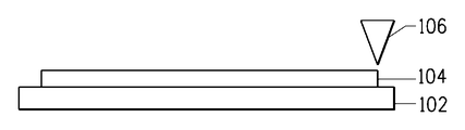
도 1은 실질적인 제조 절차를 예시하는 개략도이다. 우선, 감광성 페이스트를 유리 기재 상에 코팅한다. 디스펜서를 사용하는 스크린 인쇄 및 코팅 방법(106)에 의해서 전도성 감광성 페이스트(104)를 유리 기재(102) 상에 완전히 코팅한다(도 1(A)).1 is a schematic diagram illustrating a substantial manufacturing procedure. First, the photosensitive paste is coated on a glass substrate. The conductive
다음으로, 코팅된 감광성 페이스트를 건조시킨다. 감광성 페이스트의 층이 건조된다면 건조 조건은 특별히 한정되지 않는다. 예를 들어, 100℃에서 18 내지 20분 동안 건조시킬 수 있다. 또한, 감광성 페이스트는 컨베이어-유형 적외선 건조 기기를 사용하여 건조시킬 수 있다.Next, the coated photosensitive paste is dried. The drying conditions are not particularly limited as long as the layer of the photosensitive paste is dried. For example, it may be dried at 100 ° C. for 18 to 20 minutes. In addition, the photosensitive paste can be dried using a conveyor-type infrared drying machine.
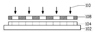
다음으로, 건조된 감광성 페이스트를 패턴화한다. 패턴화 처리에서는, 건조된 감광성 페이스트를 노광 및 현상한다. 노광 공정에서는, 전극 패턴을 갖는 포토마스크(108)를 건조된 감광성 페이스트(104) 상에 놓고 여기에 자외선(110)을 조사한다(도 3(B)).Next, the dried photosensitive paste is patterned. In the patterning process, the dried photosensitive paste is exposed and developed. In the exposure step, a
노광 조건은 감광성 페이스트의 유형 및 감광성 페이스트의 막 두께에 따라 상이하다. 예를 들어, 200 내지 400 ㎛의 간극이 사용되는 노광 공정에서는, 100 mJ/㎠ 내지 2000 mJ/㎠의 자외선을 사용하는 것이 바람직하다. 조사 기간은 바람직하게는 5 내지 200초이다.The exposure conditions differ depending on the type of photosensitive paste and the film thickness of the photosensitive paste. For example, in the exposure process in which the gap of 200-400 micrometers is used, it is preferable to use the ultraviolet-ray of 100 mJ / cm <2> -2000 mJ / cm <2>. The irradiation period is preferably 5 to 200 seconds.
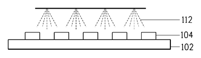
현상은 알칼리 용액에 의해 이루어질 수 있다. 알칼리 용액으로서, 0.4% 탄산나트륨 용액이 사용될 수 있다. 현상은 알칼리 용액(112)을 기재(102) 상의 노광된 감광성 페이스트 층(104)에 분무하거나(도 3(C)) 또는 노광된 감광성 페이스트(104)를 갖는 기재(102)를 알칼리 용액에 담가서 이루어질 수 있다.Development can be effected by alkaline solution. As alkaline solution, 0.4% sodium carbonate solution can be used. The development can be accomplished by spraying the
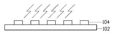
다음으로, 패턴화된 감광성 페이스트를 소결한다(도 3(D)). 조성물은 미리 결정된 온도 프로파일을 갖는 소결로에서 소결될 수 있다. 소결 공정 중 최대 온도는 바람직하게는 400 내지 600℃, 또는 더욱 바람직하게는 500 내지 600℃이다. 소결 기간은 바람직하게는 1 내지 3시간, 또는 더욱 바람직하게는 1.5시간이다.Next, the patterned photosensitive paste is sintered (FIG. 3 (D)). The composition may be sintered in a sintering furnace having a predetermined temperature profile. The maximum temperature during the sintering process is preferably 400 to 600 ° C, or more preferably 500 to 600 ° C. The sintering period is preferably 1 to 3 hours, or more preferably 1.5 hours.
본 발명에서, 소성은 공기 대기에서 수행된다. 상기에 언급된 바와 같이, 공기 소성을 사용하더라도 감광성 페이스트의 조성물을 제어함으로써 낮은 저항의, 미세한 패턴이 형성될 수 있다. 본 출원에서, "공기 중 소성" 또는 "공기 소성"은 본질적으로 소성로 내의 대기를 대체하지 않고 소성함을 의미하며, 더욱 구체적으로는 소성로 내의 대기를 대체하지 않는 소성 및 노 내의 대기 중 5 부피% 미만을 대체하는 소성 둘 모두를 포함한다.In the present invention, firing is carried out in an air atmosphere. As mentioned above, even with air firing, a low resistance, fine pattern can be formed by controlling the composition of the photosensitive paste. In the present application, "air firing" or "air firing" means firing essentially without replacing the atmosphere in the kiln, more specifically 5 vol% of the firing and the atmosphere in the furnace without replacing the atmosphere in the kiln. Both firings replacing less than.
소결 및 냉각 공정 후에, 어드레스 전극(114)을 갖는 기재(103)를 얻는다(도 3(E)).After the sintering and cooling process, a substrate 103 having an address electrode 114 is obtained (FIG. 3E).
은 페이스트와 동일한 방식으로 배선 재료로서 사용기 위하여, 체적 저항률은 은의 체적 저항률과 비교할 때 크게 초과될 수 없다(예를 들어, 100배). 체적 저항률이 너무 커지는 경우, 극도의 설계 변경이 필요하기 때문에 구리로의 대체가 매우 어려워진다. 은의 체적 저항률은 실온 근처에서 1.6×10⁻⁶ Ω?㎝이므로, 기준을 100배로 정하는 경우, 체적 저항률은 1.6×10⁻⁴ Ω?㎝ 이하인 것이 바람직하다. 본 발명에 따르면, 공기 베이킹을 수행하더라도 구리를 전도성 성분으로서 사용하여 그러한 낮은 저항의 전극을 형성하는 것이 가능하다.For use as the wiring material in the same way as the silver paste, the volume resistivity cannot be greatly exceeded when compared with the volume resistivity of silver (eg, 100 times). If the volume resistivity becomes too large, replacement with copper becomes very difficult because of extreme design changes required. Since the volume resistivity of silver is 1.6 × 10 −6 Ω · cm near room temperature, when the standard is set at 100 times, the volume resistivity is preferably 1.6 × 10 −4 Ω · cm or less. According to the present invention, it is possible to form such a low resistance electrode using copper as the conductive component even if air baking is performed.
본 발명은 전극을 갖는 전자 소자에 적용가능하나, 용도가 그에 특별히 한정되지는 않는다. 바람직하게는, 본 발명은 PDP의 후방 패널의 전극에 적용가능하다. 본 발명을 사용함으로써 PDP의 생산 비용이 감소될 수 있다.The present invention is applicable to an electronic device having an electrode, but its use is not particularly limited thereto. Preferably, the present invention is applicable to the electrodes of the rear panel of the PDP. By using the present invention, the production cost of the PDP can be reduced.
실시예Example
본 발명을 실시예에 의해 이하에서 보다 상세하게 예시한다. 실시예들은 단지 예시적인 목적을 위한 것이며, 본 발명을 한정하고자 하는 것이 아니다.The invention is illustrated in more detail below by way of examples. The examples are for illustrative purposes only and are not intended to limit the invention.
(A) 구리 및 붕소 분말 비의 효과에 대한 시험(A) Test for the effect of the ratio of copper and boron powder
1. 유기 성분의 제조1. Preparation of Organic Ingredients
용매로서 텍사놀(2,2,4-트라이메틸-1,3-펜탄다이올 모노아이소부티레이트) 및 유기 결합제로서 분자량이 6,000 내지 7,000인 아크릴 중합체 결합제를 혼합하였고, 그 혼합물을 교반하면서 100℃로 가열하였다. 유기 결합제 모두가 용해될 때까지 혼합물을 가열하고 교반하였다. 생성된 용액을 75℃로 냉각하였다. EDAB(에틸 4-다이메틸 아미노벤조에이트), DETX(다이에틸티옥산톤), 및 시바 스페셜티 케미칼즈(Chiba Specialty Chemicals)의 이르가큐어(Irgacure) 907을 광중합 개시제로서 첨가하였고, TAOBN(1,4,4-트라이메틸-2,3-다이아자바이사이클로[3.2.2]-논-2-엔-N,N-다이옥사이드)를 안정제로서 첨가하였다. 모든 고형물이 용해될 때까지 혼합물을 75℃에서 교반하였다. 40 마이크로미터 필터를 통해 용액을 여과하고 냉각시켰다.Texanol (2,2,4-trimethyl-1,3-pentanediol monoisobutyrate) as a solvent and an acrylic polymer binder having a molecular weight of 6,000 to 7,000 as an organic binder were mixed and the mixture was stirred at 100 ° C. Heated. The mixture was heated and stirred until all of the organic binder dissolved. The resulting solution was cooled to 75 ° C. EDAB (ethyl 4-dimethyl aminobenzoate), DETX (diethylthioxanthone), and Irgacure 907 from Chiba Specialty Chemicals were added as photopolymerization initiators, and TAOBN (1, 4,4-trimethyl-2,3-diazabicyclo [3.2.2] -non-2-ene-N, N-dioxide) was added as a stabilizer. The mixture was stirred at 75 ° C. until all solids dissolved. The solution was filtered and cooled through a 40 micron filter.
2. 구리 및 붕소 페이스트의 제조2. Preparation of Copper and Boron Paste
2.42 중량%의 TMPEOTA(트라이메틸올프로판 에톡시트라이아크릴레이트), 2.42 중량%의 BASF의 라로머(Laromer)(등록상표) LR8967(폴리에틸 아크릴레이트 올리고머) 및 7.26 중량%의 사토머(Sartomer)(등록상표) SE399(다이펜타에리트리톨 펜타아크릴레이트)로 이루어진 광중합 단량체, 안정제로서 0.26 중량%의 말론산, 0.04 중량%의 실리콘 소포제(비와이케이 케미(BYK Chemie), BYK085)를, 황색 광 하에 혼합 탱크에서 20.31 중량%의 상기 유기 성분과 혼합하여 페이스트를 제조하였다. 1.09 중량%의 비스무트 프릿(니폰 야마무라 글래스(Nippon Yamamura Glass)), 붕소 분말(에이치. 씨. 스타크(H. C. Starck), 붕소 무정형 I, D50=0.9㎛), 및 구리 분말(울트라파인 파우더 테크놀로지(Ultrafine Powder Technology), D50=1.0㎛)을 전도성 입자로서 사용하였다. 표 1에 나타낸 바와 같이 붕소 분말 및 구리 분말의 양은 상이한 실시예 및 비교예 간에 달랐다. 실시예 및 비교예에 사용된 양이 표 1 내지 표 3에 주어져 있다.2.42 weight percent TMPEOTA (trimethylolpropane ethoxytriacrylate), 2.42 weight percent BASF's Laromer® LR8967 (polyethyl acrylate oligomer) and 7.26 weight percent Sartomer Photopolymerization monomer consisting of SE399 (Dipentaerythritol pentaacrylate), 0.26% by weight of malonic acid as stabilizer, 0.04% by weight of silicone antifoaming agent (BYK Chemie, BYK085) under yellow light A paste was prepared by mixing with 20.31% by weight of the organic components in a mixing tank. 1.09 wt% bismuth frit (Nippon Yamamura Glass), boron powder (H. Starch, boron amorphous I, D50 = 0.9 μm), and copper powder (Ultrafine powder technology) Powder Technology), D50 = 1.0 μm) was used as the conductive particles. As shown in Table 1, the amounts of boron powder and copper powder differed between different examples and comparative examples. The amounts used in the examples and comparative examples are given in Tables 1-3.
무기 재료의 입자가 유기 재료로 습윤될 때까지 전체 페이스트를 혼합하였다. 3롤 밀을 사용하여 혼합물을 분산시켰다.The whole paste was mixed until the particles of the inorganic material were wetted with the organic material. The mixture was dispersed using a three roll mill.
3. 전극의 제조3. Preparation of Electrode
페이스트의 제조 및 부품들의 제조 동안의 먼지에 의한 오염은 결함을 초래할 것이므로, 먼지 오염을 피하도록 예방조치를 취하였다.Contamination by dust during the manufacture of the paste and the manufacture of the parts will lead to defects, so precautions have been taken to avoid dust contamination.
3-1: 코팅3-1: coating
구리 및 붕소 페이스트를 200 내지 400 메시 스크린을 사용하여 스크린 인쇄에 의해 유리 기재에 적용하였다. 원하는 막 두께가 얻어지는 것을 보장하기 위해 흑색 전극 페이스트의 적합한 점도 및 스크린을 선택하였다. 이어서, 페이스트를 고온공기순환로(hot air circulating furnace)에서 100℃로 20분 동안 건조시켜서, 건조된 막 두께가 4.5 내지 5.0 ㎛인 구리 및 붕소 전극을 형성하였다.Copper and boron paste were applied to the glass substrate by screen printing using a 200-400 mesh screen. The appropriate viscosity and screen of the black electrode paste was chosen to ensure that the desired film thickness was obtained. The paste was then dried at 100 ° C. for 20 minutes in a hot air circulating furnace to form copper and boron electrodes with a dried film thickness of 4.5 to 5.0 μm.
3-2: UV선 패턴 노광3-2: UV ray pattern exposure
시준된 UV 방사선 공급원을 사용하여 포토 툴을 통해 건조된 페이스트를 노광시켰다(조도: 18 내지 20 ㎽/㎠; 노광: 200 내지 2000mJ/㎠).The dried paste was exposed through a phototool using a collimated UV radiation source (roughness: 18-20 kPa / cm 2; exposure: 200-2000 mJ / cm 2).
3-3: 현상3-3: phenomenon
노광된 샘플을 컨베이어 상에 배치한 다음, 현상제로서 0.4 중량% 탄산나트륨 수용액으로 채워진 스프레이 현상 장치에 배치하였다. 현상제를 30℃의 온도로 유지하였고, 10 내지 20 psi로 분무하였다.The exposed sample was placed on a conveyor and then placed in a spray developing apparatus filled with 0.4 wt% aqueous sodium carbonate solution as a developer. The developer was kept at a temperature of 30 ° C. and sprayed at 10-20 psi.
현상 시간은 하기 방식으로 결정하였다. 우선 노광되지 않은 건조한 막을 현상제에서 세척하는 데 드는 시간(TTC, 세정 시간(Time To Clear))을, 그러한 건조된 노광되지 않은 샘플을 사용하여, 노광된 패턴을 갖는 샘플에 대해서와 동일한 조건 하에 인쇄하여 측정하였다. 그 다음, 노광된 패턴을 갖는 샘플 부품을 TTC의 1.5배로 설정된 현상 시간으로 현상하였다.The developing time was determined in the following manner. First, the time taken to clean the unexposed dry film in the developer (TTC, Time To Clear) was determined under the same conditions as for the sample with the exposed pattern using such a dry unexposed sample. Printed and measured. Then, the sample part having the exposed pattern was developed with a developing time set to 1.5 times TTC.
에어젯으로 여분의 물을 불어냄으로써 현상된 샘플을 건조시켰다.The developed sample was dried by blowing excess water with an air jet.
3-4: 소결3-4: Sintered
1.5 시간 프로파일을 사용하여 공기 중에서 벨트 노(belt furnace) 내에서 소결에 의해 590℃의 피크 온도에 도달하였다(제1 소결).The peak temperature of 590 ° C. was reached (first sintering) by sintering in a belt furnace in air using a 1.5 hour profile.
유기 성분의 함량 및 구리 분말의 다양한 크기를 일정하게 유지하고, 구리와 붕소의 합계 중량에 대한 붕소 중량의 비([B] / [Cu+B])를 5% 내지 50%로 변화시켜, 소성된 부품의 표면 저항을 측정하였다.The content of organic components and various sizes of the copper powder are kept constant, and the ratio of the weight of boron ([B] / [Cu + B]) to the total weight of copper and boron is changed from 5% to 50%, so as to fire The surface resistance of the finished part was measured.
표면 저항의 측정을 위해, 폴리 #380 메시 스크린을 사용하여 40 ㎜ × 40㎜ 정사각형 인쇄 영역을 형성하도록 유리 슬라이드 상에 샘플 페이스트를 스크린 인쇄하여 시험편을 제조하였다. 부품을 건조시키고, 포토마스크를 사용하지 않고 전체적으로 노광시킨 다음 소성하였다. 40 ㎜ × 40 ㎜ 영역의 대각선을 가로질러 표면 상에 2개의 탐침을 적용하여, 소성된 막의 표면 저항을 측정하였다. 이러한 측정을 위해, 소성된 막의 두께를 3 내지 5 ㎛의 범위로 조절하였다.For measurement of surface resistance, test pieces were prepared by screen printing sample paste on a glass slide to form a 40 mm × 40 mm square print area using a poly # 380 mesh screen. The parts were dried, totally exposed without using a photomask and then fired. Two probes were applied on the surface across the diagonal of the 40 mm × 40 mm area to measure the surface resistance of the fired film. For this measurement, the thickness of the fired film was adjusted in the range of 3 to 5 mu m.
하기 방법에 의해 라인 형성을 평가하였다. 패턴 노광되고 현상된 샘플 조각을 시각적으로 확인하여 현상 후에 미세 라인이 남아있는 지 아닌 지를 결정하였다. 더욱 구체적으로, 소성된 막의 두께를 3 내지 5 ㎛로 조절하면서, 100 ㎛ 라인 패턴 포토마스크를 사용하여 샘플 부품을 800 mJ/ ㎠에 노광시킨 다음, TTC의 1.5배의 현상 시간으로 현상시켰다.Line formation was evaluated by the following method. The pattern exposed and developed sample pieces were visually checked to determine whether fine lines remained after development. More specifically, the sample part was exposed to 800 mJ / cm 2 using a 100 μm line pattern photomask while adjusting the thickness of the fired film to 3 to 5 μm, and then developed at a development time of 1.5 times TTC.
100㎛ 라인이 현상 후에 남아있는 경우에 OK로 점수를 매겼다. 그러나 100 ㎛ 라인이 씻겨나갔거나 또는 다수의 단선이 관찰되는 경우에는, NG(no good)로 점수를 매겼다.Scored as OK if 100 μm line remained after development. However, if the 100 μm line was washed away or a large number of disconnections were observed, it was scored as NG (no good).
공기 소성 조건 하에서 구리 분말은 쉽게 산화되나, 붕소 중량비가 15% 및 17.5%인 샘플에서는 표면 저항이 1.0 Ω 미만이었으며, 붕소의 존재에 의해 산화가 효과적으로 억제되는 것으로 나타났다. 5 중량%의 붕소 중량을 갖는 샘플에서는, 산화가 진행되었기 때문에 저항이 1 MΩ을 초과하였고, 표면 저항이 매우 커졌다. 다른 한편, 35 중량% 및 50 중량%의 붕소 함량을 갖는 샘플에서는, 표면 저항이 장치의 측정 상한(100 MΩ)을 초과하였다. 허용 저항 값을 100 Ω으로 설정하는 경우, 구리 및 붕소의 합계 중량에 대한 붕소의 중량의 비에 있어서 5 중량%의 값은 너무 작은 것으로 여겨질 수 있고, 35 중량%의 값은 너무 큰 것으로 여겨질 수 있다. 도 2는 붕소 함량과 표면 저항 사이의 관계를 나타내는 그래프이다.Copper powder easily oxidized under air firing conditions, but the sample had a surface resistance of less than 1.0 Ω in samples with a boron weight ratio of 15% and 17.5%, and oxidation was effectively inhibited by the presence of boron. In the sample having a boron weight of 5% by weight, the resistance exceeded 1 MΩ because the oxidation proceeded, and the surface resistance became very large. On the other hand, in the samples having a boron content of 35% by weight and 50% by weight, the surface resistance exceeded the upper limit of measurement (100 MΩ) of the device. When the allowable resistance value is set to 100 Ω, the value of 5% by weight may be considered too small and the value of 35% by weight is considered too large in the ratio of the weight of boron to the total weight of copper and boron. Can lose. 2 is a graph showing the relationship between boron content and surface resistance.
[표 1][Table 1]

(B) 구리 분말의 (B) of copper powder 직경의Diameter 효과에 대한 시험 Test for effectiveness
표 2에 도시된 바와 같이, 유기 성분의 함량 및 구리와 붕소의 합계 중량에 대한 붕소의 중량([B] / [Cu+B] = 17.5 중량%)을 일정하게 유지하고, 구리 분말의 평균 입자 크기(D50)를 변화시켜, 소성된 부품에서 표면 저항을 측정하였다. 평균 입자 크기(D50)가 3 ㎛인 구리 분말을 사용하는 경우, 표면 저항이 34.1 Ω으로 증가하였고, 그러한 큰 입자 크기의 구리 분말로는 원하는 낮은 저항값을 얻기가 어려운 것으로 나타났다.As shown in Table 2, the content of the organic component and the weight of boron ([B] / [Cu + B] = 17.5 wt%) with respect to the total weight of copper and boron are kept constant, and the average particle of the copper powder By varying the size (D50), the surface resistance was measured in the fired parts. When using a copper powder having an average particle size (D50) of 3 μm, the surface resistance increased to 34.1 Ω, and it was found that it is difficult to obtain a desired low resistance value with such a large particle size copper powder.
[표 2]TABLE 2

(C) 유기 및 무기 조성물의 효과에 대한 시험(C) testing the effects of organic and inorganic compositions
구리와 붕소의 합계 중량에 대한 붕소의 중량([B] / [Cu+B])을 17.5 중량%로 일정하게 유지하였고, D50 = 1.1의 구리 분말을 사용하여, 표 3에 나타낸 페이스트들을 무기 성분 및 유기 성분의 양 또는 유기 성분 중 단량체의 양을 달리함으로써 제조하였고, 광 패턴화 및 패턴화된 라인에 관하여 베이킹 후의 체적 저항률을 결정하였다.The weight of boron ([B] / [Cu + B]) was kept constant at 17.5% by weight relative to the total weight of copper and boron, and the pastes shown in Table 3 were prepared using an inorganic powder of D50 = 1.1. And by varying the amount of the organic component or the amount of monomer in the organic component, the volume resistivity after baking with respect to the light patterning and patterned lines was determined.
라인을 형성하지 않고 측정된 표면 저항에 대해서는 전반적으로 양호한 값을 얻었다. 무기/유기 조성물의 세부사항을 조사하였을 때, 100㎛ 라인의 패턴 형성은 [무기 성분의 중량]/[유기 성분의 중량]의 값이 3.5 이하일 때 양호한 경향이 있었다. 라인 형성은 또한 [단량체의 중량]/[무기 성분의 중량]이 0.1 내지 0.3의 범위일 때 양호한 경향이 있었다. 표 3에 나타낸 바와 같이, [무기 성분의 중량]/[유기 성분의 중량]이 더 작아졌을 때 저항률이 증가하였다. [단량체의 중량]/[유기 성분의 중량]이 0.3 이상으로 증가하였을 때는 라인이 잘 형성될 수 있었으나, 저항이 증가하였고, 표면 끈적임이 증가하는 경향이 있었다.Overall good values were obtained for the surface resistance measured without forming a line. When examining the details of the inorganic / organic composition, the pattern formation of the 100 탆 line tended to be good when the value of [weight of inorganic component] / [weight of organic component] was 3.5 or less. Line formation also tended to be good when [weight of monomer] / [weight of inorganic components] ranged from 0.1 to 0.3. As shown in Table 3, the resistivity increased when [weight of inorganic component] / [weight of organic component] became smaller. When the weight of the monomer / weight of the organic component increased to 0.3 or more, the lines could be well formed, but the resistance increased and the surface stickiness tended to increase.
하기 방법에 의해 체적 저항률을 평가하였다.The volume resistivity was evaluated by the following method.
체적 저항률을 위해, 400 ㎛ 폭 및 14.7 ㎜ 길이의 라인의 패턴을 갖는 포토마스크를 사용한 노광, 현상, 및 소성에 의해 형성된 패턴 상에서 저항을 측정하였다. 라인 폭 및 막 두께로부터 체적 저항률을 계산하였다.For volume resistivity, the resistance was measured on the pattern formed by exposure, development, and firing using a photomask having a pattern of lines 400 μm wide and 14.7 mm long. Volume resistivity was calculated from line width and film thickness.
[표 3][Table 3]

[표 3][Table 3]

Claims (7)
적용된 감광성 페이스트를 건조시키는 단계;
건조된 감광성 페이스트를 노광시키는 단계;
노광된 감광성 페이스트를 현상하는 단계; 및
현상된 감광성 페이스트를 공기 중에서 소성하여 전극 패턴을 형성하는 단계를 포함하는, 플라즈마 디스플레이 패널용 전극의 제조 방법.An inorganic component containing copper powder, boron powder, and glass frit, and an organic component containing a photopolymerization initiator, a monomer, and an organic vehicle, wherein the average particle size of the copper powder is 2.5 μm or less, and the content of the boron powder is Applying from 8 to 25% by weight of the photosensitive paste, based on the total amount of copper powder and boron powder;
Drying the applied photosensitive paste;
Exposing the dried photosensitive paste;
Developing the exposed photosensitive paste; And
A method of manufacturing an electrode for a plasma display panel, comprising baking the developed photosensitive paste in air to form an electrode pattern.
Applications Claiming Priority (2)
| Application Number | Priority Date | Filing Date | Title |
|---|---|---|---|
| US12/496,920 | 2009-07-02 | ||
| US12/496,920 US8129088B2 (en) | 2009-07-02 | 2009-07-02 | Electrode and method for manufacturing the same |
Publications (1)
| Publication Number | Publication Date |
|---|---|
| KR20120032551A true KR20120032551A (en) | 2012-04-05 |
Family
ID=42537876
Family Applications (1)
| Application Number | Title | Priority Date | Filing Date |
|---|---|---|---|
| KR1020127002809A KR20120032551A (en) | 2009-07-02 | 2010-07-01 | Electrode and method for manufacturing the same |
Country Status (7)
| Country | Link |
|---|---|
| US (1) | US8129088B2 (en) |
| EP (1) | EP2449571A1 (en) |
| JP (1) | JP5654588B2 (en) |
| KR (1) | KR20120032551A (en) |
| CN (1) | CN102473563B (en) |
| TW (1) | TW201115593A (en) |
| WO (1) | WO2011002964A1 (en) |
Cited By (4)
| Publication number | Priority date | Publication date | Assignee | Title |
|---|---|---|---|---|
| WO2019074190A1 (en) * | 2017-10-12 | 2019-04-18 | 전자부품연구원 | Conductive paste composition, method for preparing same, and electrode formed from same |
| KR20190041141A (en) * | 2017-10-12 | 2019-04-22 | 전자부품연구원 | Conductive paste composition, method for preparing the composition and electrode formed by the composition |
| KR20190041145A (en) * | 2017-10-12 | 2019-04-22 | 전자부품연구원 | Conductive paste composition, method for preparing the composition and electrode formed by the composition |
| KR20230077363A (en) * | 2021-11-25 | 2023-06-01 | 한국화학연구원 | Positive photosensitive paste composition, electrode provided with conductive pattern using the same, and manufacturing method thereof |
Families Citing this family (17)
| Publication number | Priority date | Publication date | Assignee | Title |
|---|---|---|---|---|
| US20110083874A1 (en) * | 2009-10-09 | 2011-04-14 | E. I. Du Pont De Nemours And Company | Electrode and method for manufacturing the same |
| US8728355B2 (en) * | 2011-01-14 | 2014-05-20 | E. I. Du Pont De Nemours And Company | Electrode and method for manufacturing the same |
| US8709294B2 (en) * | 2011-01-28 | 2014-04-29 | E. I. Du Pont De Nemours And Company | Electrode and method for manufacturing the same |
| US8647815B1 (en) * | 2012-07-26 | 2014-02-11 | E I Du Pont De Nemours And Company | Method of manufacturing copper electrode |
| CN105009695B (en) * | 2013-02-18 | 2018-09-18 | 奥博泰克有限公司 | The direct scribe laser metallization of two steps |
| US10622244B2 (en) | 2013-02-18 | 2020-04-14 | Orbotech Ltd. | Pulsed-mode direct-write laser metallization |
| US10537027B2 (en) | 2013-08-02 | 2020-01-14 | Orbotech Ltd. | Method producing a conductive path on a substrate |
| US20150197645A1 (en) * | 2014-01-16 | 2015-07-16 | E I Du Pont De Nemours And Company | Method of manufacturing non-firing type electrode |
| WO2016029400A1 (en) | 2014-08-28 | 2016-03-03 | E.I. Du Pont De Nemours And Company | Copper-containing conductive pastes and electrodes made therefrom |
| CN106575537A (en) | 2014-08-28 | 2017-04-19 | E.I.内穆尔杜邦公司 | Solar cells with copper electrodes |
| CN106605270B (en) | 2014-08-28 | 2019-03-08 | E.I.内穆尔杜邦公司 | Cupric electrocondution slurry and thus manufactured electrode |
| US10193004B2 (en) | 2014-10-19 | 2019-01-29 | Orbotech Ltd. | LIFT printing of conductive traces onto a semiconductor substrate |
| WO2016075743A1 (en) | 2014-11-10 | 2016-05-19 | 大研化学工業株式会社 | Conductive paste for atmospheric firing and method for producing same |
| WO2016116924A1 (en) | 2015-01-19 | 2016-07-28 | Orbotech Ltd. | Printing of three-dimensional metal structures with a sacrificial support |
| US9966480B2 (en) * | 2015-04-28 | 2018-05-08 | Samsung Sdi Co., Ltd. | Electrode composition, electrode manufactured using the same, and solar cell |
| EP3377290B1 (en) | 2015-11-22 | 2023-08-02 | Orbotech Ltd. | Control of surface properties of printed three-dimensional structures |
| TW201901887A (en) | 2017-05-24 | 2019-01-01 | 以色列商奧寶科技股份有限公司 | Electrical interconnection circuit components on the substrate without prior patterning |
Family Cites Families (30)
| Publication number | Priority date | Publication date | Assignee | Title |
|---|---|---|---|---|
| NL101499C (en) | 1951-08-20 | |||
| US2850445A (en) | 1955-01-19 | 1958-09-02 | Oster Gerald | Photopolymerization |
| US2875047A (en) | 1955-01-19 | 1959-02-24 | Oster Gerald | Photopolymerization with the formation of coherent plastic masses |
| US3074974A (en) | 1957-12-06 | 1963-01-22 | Monsanto Chemicals | Method for the preparation of diglycidyl ether of tetrachlorobisphenol-a |
| US3097097A (en) | 1959-02-12 | 1963-07-09 | Gisela K Oster | Photo degrading of gel systems and photographic production of reliefs therewith |
| NL254306A (en) | 1959-08-07 | |||
| GB1090142A (en) | 1965-02-26 | 1967-11-08 | Agfa Gevaert Nv | Photochemical insolubilisation of polymers |
| US3479185A (en) | 1965-06-03 | 1969-11-18 | Du Pont | Photopolymerizable compositions and layers containing 2,4,5-triphenylimidazoyl dimers |
| US3380381A (en) * | 1965-08-06 | 1968-04-30 | Western Printing Mach Co | Rotary press printing cylinder for clamping flexible plates |
| US3549367A (en) | 1968-05-24 | 1970-12-22 | Du Pont | Photopolymerizable compositions containing triarylimidazolyl dimers and p-aminophenyl ketones |
| US4122232A (en) * | 1975-04-21 | 1978-10-24 | Engelhard Minerals & Chemicals Corporation | Air firable base metal conductors |
| US4070517A (en) * | 1976-07-08 | 1978-01-24 | Beckman Instruments, Inc. | Low fired conductive compositions |
| US4162162A (en) | 1978-05-08 | 1979-07-24 | E. I. Du Pont De Nemours And Company | Derivatives of aryl ketones and p-dialkyl-aminoarylaldehydes as visible sensitizers of photopolymerizable compositions |
| JPS5874030A (en) * | 1981-10-28 | 1983-05-04 | ティーディーケイ株式会社 | Electronic part, conductive film composition and method of producing same |
| US5047313A (en) * | 1989-08-21 | 1991-09-10 | E. I. Du Pont De Nemours And Company | Photosensitive semi-aqueous developable copper conductor composition |
| JP2841586B2 (en) * | 1989-12-04 | 1998-12-24 | 大同特殊鋼株式会社 | Conductive paste |
| JPH06349316A (en) * | 1993-06-11 | 1994-12-22 | Tdk Corp | Conductive paste |
| JP3079930B2 (en) * | 1995-01-23 | 2000-08-21 | 株式会社村田製作所 | Porcelain capacitors |
| US5851732A (en) | 1997-03-06 | 1998-12-22 | E. I. Du Pont De Nemours And Company | Plasma display panel device fabrication utilizing black electrode between substrate and conductor electrode |
| JPH11242930A (en) * | 1997-12-03 | 1999-09-07 | Toray Ind Inc | Manufacture of electrode and manufacture of member for plasma display panel |
| KR20050122498A (en) * | 2004-06-24 | 2005-12-29 | 삼성에스디아이 주식회사 | A photosensitive paste composition, the pdp electrode prepared therefrom and a pdp comprising the pdp electrode |
| JP2006030853A (en) * | 2004-07-21 | 2006-02-02 | Taiyo Ink Mfg Ltd | Photosensitive paste and baked product pattern formed using the same |
| CN100573323C (en) * | 2004-07-22 | 2009-12-23 | 东丽株式会社 | The manufacture method of photosensitive paste and member for display panel |
| US7135267B2 (en) * | 2004-08-06 | 2006-11-14 | E. I. Du Pont De Nemours And Company | Aqueous developable photoimageable compositions for use in photo-patterning methods |
| KR100658714B1 (en) * | 2004-11-30 | 2006-12-15 | 삼성에스디아이 주식회사 | Photo-sensitive composition, photo-sensitive paste composition for barrier ribs comprising the same, and method for preparing barrier ribs for plasma display panel |
| JP2007012371A (en) * | 2005-06-29 | 2007-01-18 | E I Du Pont De Nemours & Co | Method for manufacturing conductive composition and rear substrate of plasma display |
| US7655864B2 (en) * | 2006-07-13 | 2010-02-02 | E.I Du Pont De Nemours And Company | Photosensitive conductive paste for electrode formation and electrode |
| KR100829667B1 (en) * | 2006-09-07 | 2008-05-16 | 엘지전자 주식회사 | Electrode paste composite, up-board structure of plasma display panel and manufacturing method manufactured by using the same |
| KR100852705B1 (en) | 2006-09-15 | 2008-08-19 | 삼성에스디아이 주식회사 | Composition of electrode paste and plasma display panel using the same |
| US7887992B2 (en) * | 2008-12-23 | 2011-02-15 | E. I. Du Pont De Nemours And Company | Photosensitive paste and process for production of pattern using the same |
-
2009
- 2009-07-02 US US12/496,920 patent/US8129088B2/en active Active
-
2010
- 2010-07-01 EP EP10735368A patent/EP2449571A1/en not_active Withdrawn
- 2010-07-01 KR KR1020127002809A patent/KR20120032551A/en not_active Application Discontinuation
- 2010-07-01 TW TW099121709A patent/TW201115593A/en unknown
- 2010-07-01 JP JP2012517905A patent/JP5654588B2/en active Active
- 2010-07-01 WO PCT/US2010/040719 patent/WO2011002964A1/en active Application Filing
- 2010-07-01 CN CN201080027528.8A patent/CN102473563B/en active Active
Cited By (4)
| Publication number | Priority date | Publication date | Assignee | Title |
|---|---|---|---|---|
| WO2019074190A1 (en) * | 2017-10-12 | 2019-04-18 | 전자부품연구원 | Conductive paste composition, method for preparing same, and electrode formed from same |
| KR20190041141A (en) * | 2017-10-12 | 2019-04-22 | 전자부품연구원 | Conductive paste composition, method for preparing the composition and electrode formed by the composition |
| KR20190041145A (en) * | 2017-10-12 | 2019-04-22 | 전자부품연구원 | Conductive paste composition, method for preparing the composition and electrode formed by the composition |
| KR20230077363A (en) * | 2021-11-25 | 2023-06-01 | 한국화학연구원 | Positive photosensitive paste composition, electrode provided with conductive pattern using the same, and manufacturing method thereof |
Also Published As
| Publication number | Publication date |
|---|---|
| CN102473563B (en) | 2014-07-23 |
| US20110003246A1 (en) | 2011-01-06 |
| US8129088B2 (en) | 2012-03-06 |
| EP2449571A1 (en) | 2012-05-09 |
| JP5654588B2 (en) | 2015-01-14 |
| WO2011002964A1 (en) | 2011-01-06 |
| CN102473563A (en) | 2012-05-23 |
| JP2012532420A (en) | 2012-12-13 |
| TW201115593A (en) | 2011-05-01 |
Similar Documents
| Publication | Publication Date | Title |
|---|---|---|
| KR20120032551A (en) | Electrode and method for manufacturing the same | |
| JP5080743B2 (en) | Black conductive thick film composition, black electrode, and formation method thereof | |
| US20060071202A1 (en) | Photosensitive paste composition | |
| US20120255765A1 (en) | Electrode and method for manufacturing the same | |
| US7608784B2 (en) | Photosensitive conductive paste for electrode formation and electrode | |
| KR101100490B1 (en) | Electrode paste for plasma display panel and black bus electrode for plasma display panel | |
| KR100904145B1 (en) | Black conductive thick film compositions, black electrodes, and methods of forming thereof | |
| US8728355B2 (en) | Electrode and method for manufacturing the same | |
| DE60204711T2 (en) | AQUEOUS DEVELOPABLE, LIGHT-SENSITIVE LAYER-LAYER COMPOSITION COMPOSITIONS FOR THE PRODUCTION OF BLACK ELECTRODES | |
| KR101195639B1 (en) | Polymer solutions, aqueous developable thick film compositions, processes of making and electrodes formed thereof | |
| KR100799062B1 (en) | Method for manufacturing a conductive composition and a rear substrate of a plasma display | |
| US8709294B2 (en) | Electrode and method for manufacturing the same | |
| JP5421391B2 (en) | Front electrode of PDP | |
| JP2014063705A (en) | Method of manufacturing pdp bus electrode | |
| KR100589339B1 (en) | Photosensitive conductive composition for display device | |
| KR20060029546A (en) | Photosensitive paste composition, a pdp electrode prepared therefrom, and a pdp comprising the same |
Legal Events
| Date | Code | Title | Description |
|---|---|---|---|
| A201 | Request for examination | ||
| E902 | Notification of reason for refusal | ||
| E601 | Decision to refuse application |