KR20100065305A - 멀티 엘리먼트 패키지 내에서의 인터커넥트 - Google Patents
멀티 엘리먼트 패키지 내에서의 인터커넥트 Download PDFInfo
- Publication number
- KR20100065305A KR20100065305A KR1020107004435A KR20107004435A KR20100065305A KR 20100065305 A KR20100065305 A KR 20100065305A KR 1020107004435 A KR1020107004435 A KR 1020107004435A KR 20107004435 A KR20107004435 A KR 20107004435A KR 20100065305 A KR20100065305 A KR 20100065305A
- Authority
- KR
- South Korea
- Prior art keywords
- connector block
- semiconductor device
- forming
- polymer layer
- layer
- Prior art date
- Legal status (The legal status is an assumption and is not a legal conclusion. Google has not performed a legal analysis and makes no representation as to the accuracy of the status listed.)
- Withdrawn
Links
Images


Classifications
-
- H—ELECTRICITY
- H10—SEMICONDUCTOR DEVICES; ELECTRIC SOLID-STATE DEVICES NOT OTHERWISE PROVIDED FOR
- H10W—GENERIC PACKAGES, INTERCONNECTIONS, CONNECTORS OR OTHER CONSTRUCTIONAL DETAILS OF DEVICES COVERED BY CLASS H10
- H10W70/00—Package substrates; Interposers; Redistribution layers [RDL]
- H10W70/60—Insulating or insulated package substrates; Interposers; Redistribution layers
- H10W70/611—Insulating or insulated package substrates; Interposers; Redistribution layers for connecting multiple chips together
- H10W70/614—Insulating or insulated package substrates; Interposers; Redistribution layers for connecting multiple chips together the multiple chips being integrally enclosed
-
- H—ELECTRICITY
- H10—SEMICONDUCTOR DEVICES; ELECTRIC SOLID-STATE DEVICES NOT OTHERWISE PROVIDED FOR
- H10P—GENERIC PROCESSES OR APPARATUS FOR THE MANUFACTURE OR TREATMENT OF DEVICES COVERED BY CLASS H10
- H10P72/00—Handling or holding of wafers, substrates or devices during manufacture or treatment thereof
- H10P72/70—Handling or holding of wafers, substrates or devices during manufacture or treatment thereof for supporting or gripping
- H10P72/74—Handling or holding of wafers, substrates or devices during manufacture or treatment thereof for supporting or gripping using temporarily an auxiliary support
-
- H—ELECTRICITY
- H10—SEMICONDUCTOR DEVICES; ELECTRIC SOLID-STATE DEVICES NOT OTHERWISE PROVIDED FOR
- H10W—GENERIC PACKAGES, INTERCONNECTIONS, CONNECTORS OR OTHER CONSTRUCTIONAL DETAILS OF DEVICES COVERED BY CLASS H10
- H10W44/00—Electrical arrangements for controlling or matching impedance
- H10W44/20—Electrical arrangements for controlling or matching impedance at high-frequency [HF] or radio frequency [RF]
-
- H—ELECTRICITY
- H10—SEMICONDUCTOR DEVICES; ELECTRIC SOLID-STATE DEVICES NOT OTHERWISE PROVIDED FOR
- H10W—GENERIC PACKAGES, INTERCONNECTIONS, CONNECTORS OR OTHER CONSTRUCTIONAL DETAILS OF DEVICES COVERED BY CLASS H10
- H10W70/00—Package substrates; Interposers; Redistribution layers [RDL]
- H10W70/01—Manufacture or treatment
- H10W70/05—Manufacture or treatment of insulating or insulated package substrates, or of interposers, or of redistribution layers
- H10W70/08—Manufacture or treatment of insulating or insulated package substrates, or of interposers, or of redistribution layers by depositing layers on the chip or wafer, e.g. "chip-first" RDLs
- H10W70/09—Manufacture or treatment of insulating or insulated package substrates, or of interposers, or of redistribution layers by depositing layers on the chip or wafer, e.g. "chip-first" RDLs extending onto an encapsulation that laterally surrounds the chip or wafer, e.g. fan-out wafer level package [FOWLP] RDLs
-
- H—ELECTRICITY
- H10—SEMICONDUCTOR DEVICES; ELECTRIC SOLID-STATE DEVICES NOT OTHERWISE PROVIDED FOR
- H10W—GENERIC PACKAGES, INTERCONNECTIONS, CONNECTORS OR OTHER CONSTRUCTIONAL DETAILS OF DEVICES COVERED BY CLASS H10
- H10W70/00—Package substrates; Interposers; Redistribution layers [RDL]
- H10W70/60—Insulating or insulated package substrates; Interposers; Redistribution layers
- H10W70/611—Insulating or insulated package substrates; Interposers; Redistribution layers for connecting multiple chips together
-
- H—ELECTRICITY
- H10—SEMICONDUCTOR DEVICES; ELECTRIC SOLID-STATE DEVICES NOT OTHERWISE PROVIDED FOR
- H10W—GENERIC PACKAGES, INTERCONNECTIONS, CONNECTORS OR OTHER CONSTRUCTIONAL DETAILS OF DEVICES COVERED BY CLASS H10
- H10W70/00—Package substrates; Interposers; Redistribution layers [RDL]
- H10W70/60—Insulating or insulated package substrates; Interposers; Redistribution layers
- H10W70/62—Insulating or insulated package substrates; Interposers; Redistribution layers characterised by their interconnections
- H10W70/63—Vias, e.g. via plugs
- H10W70/635—Through-vias
-
- H—ELECTRICITY
- H10—SEMICONDUCTOR DEVICES; ELECTRIC SOLID-STATE DEVICES NOT OTHERWISE PROVIDED FOR
- H10W—GENERIC PACKAGES, INTERCONNECTIONS, CONNECTORS OR OTHER CONSTRUCTIONAL DETAILS OF DEVICES COVERED BY CLASS H10
- H10W72/00—Interconnections or connectors in packages
- H10W72/01—Manufacture or treatment
- H10W72/0198—Manufacture or treatment batch processes
-
- H—ELECTRICITY
- H10—SEMICONDUCTOR DEVICES; ELECTRIC SOLID-STATE DEVICES NOT OTHERWISE PROVIDED FOR
- H10W—GENERIC PACKAGES, INTERCONNECTIONS, CONNECTORS OR OTHER CONSTRUCTIONAL DETAILS OF DEVICES COVERED BY CLASS H10
- H10W74/00—Encapsulations, e.g. protective coatings
- H10W74/10—Encapsulations, e.g. protective coatings characterised by their shape or disposition
- H10W74/111—Encapsulations, e.g. protective coatings characterised by their shape or disposition the semiconductor body being completely enclosed
- H10W74/114—Encapsulations, e.g. protective coatings characterised by their shape or disposition the semiconductor body being completely enclosed by a substrate and the encapsulations
-
- H—ELECTRICITY
- H10—SEMICONDUCTOR DEVICES; ELECTRIC SOLID-STATE DEVICES NOT OTHERWISE PROVIDED FOR
- H10W—GENERIC PACKAGES, INTERCONNECTIONS, CONNECTORS OR OTHER CONSTRUCTIONAL DETAILS OF DEVICES COVERED BY CLASS H10
- H10W90/00—Package configurations
-
- H—ELECTRICITY
- H10—SEMICONDUCTOR DEVICES; ELECTRIC SOLID-STATE DEVICES NOT OTHERWISE PROVIDED FOR
- H10W—GENERIC PACKAGES, INTERCONNECTIONS, CONNECTORS OR OTHER CONSTRUCTIONAL DETAILS OF DEVICES COVERED BY CLASS H10
- H10W90/00—Package configurations
- H10W90/401—Package configurations characterised by multiple insulating or insulated package substrates, interposers or RDLs
-
- H—ELECTRICITY
- H10—SEMICONDUCTOR DEVICES; ELECTRIC SOLID-STATE DEVICES NOT OTHERWISE PROVIDED FOR
- H10P—GENERIC PROCESSES OR APPARATUS FOR THE MANUFACTURE OR TREATMENT OF DEVICES COVERED BY CLASS H10
- H10P72/00—Handling or holding of wafers, substrates or devices during manufacture or treatment thereof
- H10P72/70—Handling or holding of wafers, substrates or devices during manufacture or treatment thereof for supporting or gripping
- H10P72/74—Handling or holding of wafers, substrates or devices during manufacture or treatment thereof for supporting or gripping using temporarily an auxiliary support
- H10P72/743—Handling or holding of wafers, substrates or devices during manufacture or treatment thereof for supporting or gripping using temporarily an auxiliary support used as a support during manufacture of interconnect decals or build up layers
-
- H—ELECTRICITY
- H10—SEMICONDUCTOR DEVICES; ELECTRIC SOLID-STATE DEVICES NOT OTHERWISE PROVIDED FOR
- H10W—GENERIC PACKAGES, INTERCONNECTIONS, CONNECTORS OR OTHER CONSTRUCTIONAL DETAILS OF DEVICES COVERED BY CLASS H10
- H10W44/00—Electrical arrangements for controlling or matching impedance
- H10W44/20—Electrical arrangements for controlling or matching impedance at high-frequency [HF] or radio frequency [RF]
- H10W44/203—Electrical connections
- H10W44/209—Vertical interconnections, e.g. vias
- H10W44/212—Coaxial feed-throughs in substrates
-
- H—ELECTRICITY
- H10—SEMICONDUCTOR DEVICES; ELECTRIC SOLID-STATE DEVICES NOT OTHERWISE PROVIDED FOR
- H10W—GENERIC PACKAGES, INTERCONNECTIONS, CONNECTORS OR OTHER CONSTRUCTIONAL DETAILS OF DEVICES COVERED BY CLASS H10
- H10W44/00—Electrical arrangements for controlling or matching impedance
- H10W44/20—Electrical arrangements for controlling or matching impedance at high-frequency [HF] or radio frequency [RF]
- H10W44/241—Electrical arrangements for controlling or matching impedance at high-frequency [HF] or radio frequency [RF] for passive devices or passive elements
- H10W44/248—Electrical arrangements for controlling or matching impedance at high-frequency [HF] or radio frequency [RF] for passive devices or passive elements for antennas
-
- H—ELECTRICITY
- H10—SEMICONDUCTOR DEVICES; ELECTRIC SOLID-STATE DEVICES NOT OTHERWISE PROVIDED FOR
- H10W—GENERIC PACKAGES, INTERCONNECTIONS, CONNECTORS OR OTHER CONSTRUCTIONAL DETAILS OF DEVICES COVERED BY CLASS H10
- H10W44/00—Electrical arrangements for controlling or matching impedance
- H10W44/501—Inductive arrangements
-
- H—ELECTRICITY
- H10—SEMICONDUCTOR DEVICES; ELECTRIC SOLID-STATE DEVICES NOT OTHERWISE PROVIDED FOR
- H10W—GENERIC PACKAGES, INTERCONNECTIONS, CONNECTORS OR OTHER CONSTRUCTIONAL DETAILS OF DEVICES COVERED BY CLASS H10
- H10W74/00—Encapsulations, e.g. protective coatings
- H10W74/01—Manufacture or treatment
- H10W74/019—Manufacture or treatment using temporary auxiliary substrates
-
- H—ELECTRICITY
- H10—SEMICONDUCTOR DEVICES; ELECTRIC SOLID-STATE DEVICES NOT OTHERWISE PROVIDED FOR
- H10W—GENERIC PACKAGES, INTERCONNECTIONS, CONNECTORS OR OTHER CONSTRUCTIONAL DETAILS OF DEVICES COVERED BY CLASS H10
- H10W74/00—Encapsulations, e.g. protective coatings
- H10W74/10—Encapsulations, e.g. protective coatings characterised by their shape or disposition
- H10W74/111—Encapsulations, e.g. protective coatings characterised by their shape or disposition the semiconductor body being completely enclosed
- H10W74/129—Encapsulations, e.g. protective coatings characterised by their shape or disposition the semiconductor body being completely enclosed forming a chip-scale package [CSP]
Landscapes
- Internal Circuitry In Semiconductor Integrated Circuit Devices (AREA)
- Variable-Direction Aerials And Aerial Arrays (AREA)
- Details Of Aerials (AREA)
Applications Claiming Priority (2)
| Application Number | Priority Date | Filing Date | Title |
|---|---|---|---|
| US11/846,874 | 2007-08-29 | ||
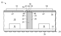
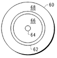
| US11/846,874 US7838420B2 (en) | 2007-08-29 | 2007-08-29 | Method for forming a packaged semiconductor device |
Publications (1)
| Publication Number | Publication Date |
|---|---|
| KR20100065305A true KR20100065305A (ko) | 2010-06-16 |
Family
ID=40406108
Family Applications (1)
| Application Number | Title | Priority Date | Filing Date |
|---|---|---|---|
| KR1020107004435A Withdrawn KR20100065305A (ko) | 2007-08-29 | 2008-07-09 | 멀티 엘리먼트 패키지 내에서의 인터커넥트 |
Country Status (7)
| Country | Link |
|---|---|
| US (1) | US7838420B2 (enExample) |
| EP (1) | EP2195840A4 (enExample) |
| JP (1) | JP5397962B2 (enExample) |
| KR (1) | KR20100065305A (enExample) |
| CN (1) | CN101790788A (enExample) |
| TW (1) | TWI451551B (enExample) |
| WO (1) | WO2009032398A1 (enExample) |
Families Citing this family (23)
| Publication number | Priority date | Publication date | Assignee | Title |
|---|---|---|---|---|
| JP2010245107A (ja) * | 2009-04-01 | 2010-10-28 | Shinko Electric Ind Co Ltd | 半導体装置及びその製造方法 |
| US8407890B2 (en) | 2010-01-25 | 2013-04-02 | Freescale Semiconductor Inc. | Method of manufacting an electronic device module with integrated antenna structure |
| US9142502B2 (en) | 2011-08-31 | 2015-09-22 | Zhiwei Gong | Semiconductor device packaging having pre-encapsulation through via formation using drop-in signal conduits |
| US8916421B2 (en) | 2011-08-31 | 2014-12-23 | Freescale Semiconductor, Inc. | Semiconductor device packaging having pre-encapsulation through via formation using lead frames with attached signal conduits |
| US8597983B2 (en) | 2011-11-18 | 2013-12-03 | Freescale Semiconductor, Inc. | Semiconductor device packaging having substrate with pre-encapsulation through via formation |
| JP5834907B2 (ja) * | 2011-12-28 | 2015-12-24 | 富士通株式会社 | 半導体装置、半導体装置の製造方法及び電子装置 |
| US9842798B2 (en) | 2012-03-23 | 2017-12-12 | STATS ChipPAC Pte. Ltd. | Semiconductor device and method of forming a PoP device with embedded vertical interconnect units |
| US9837303B2 (en) | 2012-03-23 | 2017-12-05 | STATS ChipPAC Pte. Ltd. | Semiconductor method and device of forming a fan-out device with PWB vertical interconnect units |
| US8810024B2 (en) * | 2012-03-23 | 2014-08-19 | Stats Chippac Ltd. | Semiconductor method and device of forming a fan-out PoP device with PWB vertical interconnect units |
| US10049964B2 (en) | 2012-03-23 | 2018-08-14 | STATS ChipPAC Pte. Ltd. | Semiconductor device and method of forming a fan-out PoP device with PWB vertical interconnect units |
| CN103311141B (zh) * | 2013-07-05 | 2016-01-20 | 北京理工大学 | 一种同轴垂直互连导电体的制作方法 |
| US8822268B1 (en) | 2013-07-17 | 2014-09-02 | Freescale Semiconductor, Inc. | Redistributed chip packages containing multiple components and methods for the fabrication thereof |
| US9362234B2 (en) | 2014-01-07 | 2016-06-07 | Freescale Semiconductor, Inc. | Shielded device packages having antennas and related fabrication methods |
| US10354958B2 (en) | 2014-10-01 | 2019-07-16 | Nxp Usa, Inc. | Through package circuit in fan-out wafer level package |
| US9666930B2 (en) | 2014-10-23 | 2017-05-30 | Nxp Usa, Inc. | Interface between a semiconductor die and a waveguide, where the interface is covered by a molding compound |
| TWI652775B (zh) | 2016-01-11 | 2019-03-01 | 矽品精密工業股份有限公司 | 電子封裝件 |
| US10236260B2 (en) | 2016-06-30 | 2019-03-19 | Nxp Usa, Inc. | Shielded package with integrated antenna |
| WO2019039335A1 (ja) * | 2017-08-21 | 2019-02-28 | 株式会社村田製作所 | 電子部品の製造方法及び電子部品 |
| US11557565B2 (en) | 2020-10-06 | 2023-01-17 | Nxp Usa, Inc. | Semiconductor device assembly and method therefor |
| US11502054B2 (en) | 2020-11-11 | 2022-11-15 | Nxp Usa, Inc. | Semiconductor device assembly and method therefor |
| CN114243287B (zh) * | 2021-12-10 | 2025-08-29 | 上海微波技术研究所(中国电子科技集团公司第五十研究所) | 毫米波相控阵天线阵列集成转换接头 |
| US20240088068A1 (en) * | 2022-09-08 | 2024-03-14 | Nxp Usa, Inc. | Semiconductor device with through package via and method therefor |
| US20250218977A1 (en) * | 2023-12-29 | 2025-07-03 | International Business Machines Corporation | Coaxial through insulator via between chiplets |
Family Cites Families (26)
| Publication number | Priority date | Publication date | Assignee | Title |
|---|---|---|---|---|
| JPS56115553A (en) * | 1980-02-18 | 1981-09-10 | Fujitsu Ltd | Method of mounting integrated circuit |
| JPH10303363A (ja) * | 1997-04-30 | 1998-11-13 | Sony Corp | 電子部品及びその製造方法 |
| US5949030A (en) * | 1997-11-14 | 1999-09-07 | International Business Machines Corporation | Vias and method for making the same in organic board and chip carriers |
| US6054389A (en) * | 1997-12-29 | 2000-04-25 | Vanguard International Semiconductor Corporation | Method of forming metal conducting pillars |
| US6081989A (en) * | 1998-04-30 | 2000-07-04 | Lockheed Martin Corporation | Fabrication of circuit modules with a transmission line |
| JP2000252407A (ja) * | 1999-03-04 | 2000-09-14 | Hitachi Ltd | マルチチップモジュール |
| JP2001094034A (ja) * | 1999-09-27 | 2001-04-06 | Nec Eng Ltd | ハイブリッドicパッケージ |
| US6538210B2 (en) * | 1999-12-20 | 2003-03-25 | Matsushita Electric Industrial Co., Ltd. | Circuit component built-in module, radio device having the same, and method for producing the same |
| US6444576B1 (en) | 2000-06-16 | 2002-09-03 | Chartered Semiconductor Manufacturing, Ltd. | Three dimensional IC package module |
| JP2002343927A (ja) * | 2000-07-12 | 2002-11-29 | Hitachi Maxell Ltd | 半導体モジュール及びその製造方法 |
| US7190080B1 (en) | 2000-10-13 | 2007-03-13 | Bridge Semiconductor Corporation | Semiconductor chip assembly with embedded metal pillar |
| JP2002184934A (ja) * | 2000-12-13 | 2002-06-28 | Shinko Electric Ind Co Ltd | 半導体装置及びその製造方法 |
| US6593644B2 (en) | 2001-04-19 | 2003-07-15 | International Business Machines Corporation | System of a package fabricated on a semiconductor or dielectric wafer with wiring on one face, vias extending through the wafer, and external connections on the opposing face |
| JP2003188340A (ja) * | 2001-12-19 | 2003-07-04 | Matsushita Electric Ind Co Ltd | 部品内蔵モジュールとその製造方法 |
| US6753600B1 (en) | 2003-01-28 | 2004-06-22 | Thin Film Module, Inc. | Structure of a substrate for a high density semiconductor package |
| JP4141857B2 (ja) * | 2003-02-18 | 2008-08-27 | 日立マクセル株式会社 | 半導体装置 |
| US6921975B2 (en) * | 2003-04-18 | 2005-07-26 | Freescale Semiconductor, Inc. | Circuit device with at least partial packaging, exposed active surface and a voltage reference plane |
| US6838776B2 (en) * | 2003-04-18 | 2005-01-04 | Freescale Semiconductor, Inc. | Circuit device with at least partial packaging and method for forming |
| JP2004327641A (ja) * | 2003-04-24 | 2004-11-18 | Tdk Corp | 電子部品モジュール |
| DE10320646A1 (de) | 2003-05-07 | 2004-09-16 | Infineon Technologies Ag | Elektronisches Bauteil, sowie Systemträger und Nutzen zur Herstellung desselben |
| JP2005033141A (ja) * | 2003-07-11 | 2005-02-03 | Sony Corp | 半導体装置及びその製造方法、疑似ウェーハ及びその製造方法、並びに半導体装置の実装構造 |
| US7369718B2 (en) | 2004-01-23 | 2008-05-06 | Intel Corporation | Package substrate pattern to accommodate optical waveguide |
| US20050167797A1 (en) | 2004-01-29 | 2005-08-04 | Advanpack Solutions Pte Ltd | Structure package |
| JP4615962B2 (ja) * | 2004-10-22 | 2011-01-19 | ルネサスエレクトロニクス株式会社 | 半導体装置 |
| US7476918B2 (en) * | 2004-11-22 | 2009-01-13 | Panasonic Corporation | Semiconductor integrated circuit device and vehicle-mounted radar system using the same |
| WO2007034629A1 (ja) * | 2005-09-20 | 2007-03-29 | Murata Manufacturing Co., Ltd. | 部品内蔵モジュールの製造方法および部品内蔵モジュール |
-
2007
- 2007-08-29 US US11/846,874 patent/US7838420B2/en active Active
-
2008
- 2008-07-09 KR KR1020107004435A patent/KR20100065305A/ko not_active Withdrawn
- 2008-07-09 JP JP2010522993A patent/JP5397962B2/ja active Active
- 2008-07-09 EP EP08781552A patent/EP2195840A4/en not_active Ceased
- 2008-07-09 CN CN200880104602.4A patent/CN101790788A/zh active Pending
- 2008-07-09 WO PCT/US2008/069516 patent/WO2009032398A1/en not_active Ceased
- 2008-07-15 TW TW097126735A patent/TWI451551B/zh active
Also Published As
| Publication number | Publication date |
|---|---|
| EP2195840A1 (en) | 2010-06-16 |
| US7838420B2 (en) | 2010-11-23 |
| WO2009032398A1 (en) | 2009-03-12 |
| JP5397962B2 (ja) | 2014-01-22 |
| CN101790788A (zh) | 2010-07-28 |
| EP2195840A4 (en) | 2011-01-19 |
| TWI451551B (zh) | 2014-09-01 |
| US20090057849A1 (en) | 2009-03-05 |
| JP2010538463A (ja) | 2010-12-09 |
| TW200913206A (en) | 2009-03-16 |
Similar Documents
| Publication | Publication Date | Title |
|---|---|---|
| US7838420B2 (en) | Method for forming a packaged semiconductor device | |
| US8232657B2 (en) | Packaged semiconductor assemblies and methods for manufacturing such assemblies | |
| CN111933591B (zh) | 扇出型电磁屏蔽封装结构和封装方法 | |
| US20130026657A1 (en) | Semiconductor package and method of fabricating the same | |
| US11728234B2 (en) | Electronic package comprising wire inside an electronic component and manufacturing method thereof | |
| TW200828523A (en) | Multi-component package with both top and bottom side connection pads for three-dimensional packaging | |
| CN112204719A (zh) | 晶圆级制造具有平面网格阵列接口的设备的系统和方法 | |
| US6790760B1 (en) | Method of manufacturing an integrated circuit package | |
| US6465882B1 (en) | Integrated circuit package having partially exposed conductive layer | |
| US8283780B2 (en) | Surface mount semiconductor device | |
| US20180053753A1 (en) | Stackable molded packages and methods of manufacture thereof | |
| KR20160020566A (ko) | 제1 및 제2 구성요소들의 조립 후에 금속 커넥터를 도금함으로써 마이크로전자 조립체를 형성하는 방법 및 대응하는 장치 | |
| US20150084171A1 (en) | No-lead semiconductor package and method of manufacturing the same | |
| CA2915410C (en) | Mixed impedance bond wire connections and method of making the same | |
| CN102683298B (zh) | 无承载板的封装件及其制法 | |
| KR20230019926A (ko) | 반도체 장치 및 반도체 장치의 제조 방법 | |
| KR102058247B1 (ko) | 인쇄회로기판을 이용한 반도체 패키지 | |
| CN201594536U (zh) | 芯片堆栈电路结构 | |
| US9786515B1 (en) | Semiconductor device package and methods of manufacture thereof | |
| KR102040171B1 (ko) | 인쇄회로기판을 이용한 반도체 패키지 | |
| US8022516B2 (en) | Metal leadframe package with secure feature | |
| KR101659354B1 (ko) | 반도체 패키지 및 이의 제조 방법 | |
| CN121398631A (zh) | 扇出型晶圆级封装单元 |
Legal Events
| Date | Code | Title | Description |
|---|---|---|---|
| PA0105 | International application |
St.27 status event code: A-0-1-A10-A15-nap-PA0105 |
|
| PG1501 | Laying open of application |
St.27 status event code: A-1-1-Q10-Q12-nap-PG1501 |
|
| R18-X000 | Changes to party contact information recorded |
St.27 status event code: A-3-3-R10-R18-oth-X000 |
|
| R18-X000 | Changes to party contact information recorded |
St.27 status event code: A-3-3-R10-R18-oth-X000 |
|
| R18-X000 | Changes to party contact information recorded |
St.27 status event code: A-3-3-R10-R18-oth-X000 |
|
| R18-X000 | Changes to party contact information recorded |
St.27 status event code: A-3-3-R10-R18-oth-X000 |
|
| PC1203 | Withdrawal of no request for examination |
St.27 status event code: N-1-6-B10-B12-nap-PC1203 |
|
| WITN | Application deemed withdrawn, e.g. because no request for examination was filed or no examination fee was paid | ||
| P22-X000 | Classification modified |
St.27 status event code: A-2-2-P10-P22-nap-X000 |
|
| PN2301 | Change of applicant |
St.27 status event code: A-3-3-R10-R13-asn-PN2301 St.27 status event code: A-3-3-R10-R11-asn-PN2301 |
|
| P22-X000 | Classification modified |
St.27 status event code: A-2-2-P10-P22-nap-X000 |
|
| P22-X000 | Classification modified |
St.27 status event code: A-2-2-P10-P22-nap-X000 |
|
| P22-X000 | Classification modified |
St.27 status event code: A-2-2-P10-P22-nap-X000 |