KR20100065305A - Interconnect in a multi-element package - Google Patents
Interconnect in a multi-element package Download PDFInfo
- Publication number
- KR20100065305A KR20100065305A KR1020107004435A KR20107004435A KR20100065305A KR 20100065305 A KR20100065305 A KR 20100065305A KR 1020107004435 A KR1020107004435 A KR 1020107004435A KR 20107004435 A KR20107004435 A KR 20107004435A KR 20100065305 A KR20100065305 A KR 20100065305A
- Authority
- KR
- South Korea
- Prior art keywords
- connector block
- semiconductor device
- forming
- polymer layer
- layer
- Prior art date
Links
Images


Classifications
-
- H—ELECTRICITY
- H01—ELECTRIC ELEMENTS
- H01L—SEMICONDUCTOR DEVICES NOT COVERED BY CLASS H10
- H01L23/00—Details of semiconductor or other solid state devices
- H01L23/52—Arrangements for conducting electric current within the device in operation from one component to another, i.e. interconnections, e.g. wires, lead frames
- H01L23/538—Arrangements for conducting electric current within the device in operation from one component to another, i.e. interconnections, e.g. wires, lead frames the interconnection structure between a plurality of semiconductor chips being formed on, or in, insulating substrates
- H01L23/5389—Arrangements for conducting electric current within the device in operation from one component to another, i.e. interconnections, e.g. wires, lead frames the interconnection structure between a plurality of semiconductor chips being formed on, or in, insulating substrates the chips being integrally enclosed by the interconnect and support structures
-
- H—ELECTRICITY
- H01—ELECTRIC ELEMENTS
- H01L—SEMICONDUCTOR DEVICES NOT COVERED BY CLASS H10
- H01L21/00—Processes or apparatus adapted for the manufacture or treatment of semiconductor or solid state devices or of parts thereof
- H01L21/67—Apparatus specially adapted for handling semiconductor or electric solid state devices during manufacture or treatment thereof; Apparatus specially adapted for handling wafers during manufacture or treatment of semiconductor or electric solid state devices or components ; Apparatus not specifically provided for elsewhere
- H01L21/683—Apparatus specially adapted for handling semiconductor or electric solid state devices during manufacture or treatment thereof; Apparatus specially adapted for handling wafers during manufacture or treatment of semiconductor or electric solid state devices or components ; Apparatus not specifically provided for elsewhere for supporting or gripping
- H01L21/6835—Apparatus specially adapted for handling semiconductor or electric solid state devices during manufacture or treatment thereof; Apparatus specially adapted for handling wafers during manufacture or treatment of semiconductor or electric solid state devices or components ; Apparatus not specifically provided for elsewhere for supporting or gripping using temporarily an auxiliary support
-
- H—ELECTRICITY
- H01—ELECTRIC ELEMENTS
- H01L—SEMICONDUCTOR DEVICES NOT COVERED BY CLASS H10
- H01L23/00—Details of semiconductor or other solid state devices
- H01L23/28—Encapsulations, e.g. encapsulating layers, coatings, e.g. for protection
- H01L23/31—Encapsulations, e.g. encapsulating layers, coatings, e.g. for protection characterised by the arrangement or shape
- H01L23/3107—Encapsulations, e.g. encapsulating layers, coatings, e.g. for protection characterised by the arrangement or shape the device being completely enclosed
- H01L23/3121—Encapsulations, e.g. encapsulating layers, coatings, e.g. for protection characterised by the arrangement or shape the device being completely enclosed a substrate forming part of the encapsulation
-
- H—ELECTRICITY
- H01—ELECTRIC ELEMENTS
- H01L—SEMICONDUCTOR DEVICES NOT COVERED BY CLASS H10
- H01L23/00—Details of semiconductor or other solid state devices
- H01L23/52—Arrangements for conducting electric current within the device in operation from one component to another, i.e. interconnections, e.g. wires, lead frames
- H01L23/538—Arrangements for conducting electric current within the device in operation from one component to another, i.e. interconnections, e.g. wires, lead frames the interconnection structure between a plurality of semiconductor chips being formed on, or in, insulating substrates
- H01L23/5384—Conductive vias through the substrate with or without pins, e.g. buried coaxial conductors
-
- H—ELECTRICITY
- H01—ELECTRIC ELEMENTS
- H01L—SEMICONDUCTOR DEVICES NOT COVERED BY CLASS H10
- H01L23/00—Details of semiconductor or other solid state devices
- H01L23/52—Arrangements for conducting electric current within the device in operation from one component to another, i.e. interconnections, e.g. wires, lead frames
- H01L23/538—Arrangements for conducting electric current within the device in operation from one component to another, i.e. interconnections, e.g. wires, lead frames the interconnection structure between a plurality of semiconductor chips being formed on, or in, insulating substrates
- H01L23/5385—Assembly of a plurality of insulating substrates
-
- H—ELECTRICITY
- H01—ELECTRIC ELEMENTS
- H01L—SEMICONDUCTOR DEVICES NOT COVERED BY CLASS H10
- H01L23/00—Details of semiconductor or other solid state devices
- H01L23/58—Structural electrical arrangements for semiconductor devices not otherwise provided for, e.g. in combination with batteries
- H01L23/64—Impedance arrangements
- H01L23/66—High-frequency adaptations
-
- H—ELECTRICITY
- H01—ELECTRIC ELEMENTS
- H01L—SEMICONDUCTOR DEVICES NOT COVERED BY CLASS H10
- H01L24/00—Arrangements for connecting or disconnecting semiconductor or solid-state bodies; Methods or apparatus related thereto
- H01L24/01—Means for bonding being attached to, or being formed on, the surface to be connected, e.g. chip-to-package, die-attach, "first-level" interconnects; Manufacturing methods related thereto
- H01L24/18—High density interconnect [HDI] connectors; Manufacturing methods related thereto
- H01L24/19—Manufacturing methods of high density interconnect preforms
-
- H—ELECTRICITY
- H01—ELECTRIC ELEMENTS
- H01L—SEMICONDUCTOR DEVICES NOT COVERED BY CLASS H10
- H01L24/00—Arrangements for connecting or disconnecting semiconductor or solid-state bodies; Methods or apparatus related thereto
- H01L24/01—Means for bonding being attached to, or being formed on, the surface to be connected, e.g. chip-to-package, die-attach, "first-level" interconnects; Manufacturing methods related thereto
- H01L24/18—High density interconnect [HDI] connectors; Manufacturing methods related thereto
- H01L24/20—Structure, shape, material or disposition of high density interconnect preforms
-
- H—ELECTRICITY
- H01—ELECTRIC ELEMENTS
- H01L—SEMICONDUCTOR DEVICES NOT COVERED BY CLASS H10
- H01L24/00—Arrangements for connecting or disconnecting semiconductor or solid-state bodies; Methods or apparatus related thereto
- H01L24/93—Batch processes
- H01L24/95—Batch processes at chip-level, i.e. with connecting carried out on a plurality of singulated devices, i.e. on diced chips
- H01L24/96—Batch processes at chip-level, i.e. with connecting carried out on a plurality of singulated devices, i.e. on diced chips the devices being encapsulated in a common layer, e.g. neo-wafer or pseudo-wafer, said common layer being separable into individual assemblies after connecting
-
- H—ELECTRICITY
- H01—ELECTRIC ELEMENTS
- H01L—SEMICONDUCTOR DEVICES NOT COVERED BY CLASS H10
- H01L25/00—Assemblies consisting of a plurality of individual semiconductor or other solid state devices ; Multistep manufacturing processes thereof
- H01L25/03—Assemblies consisting of a plurality of individual semiconductor or other solid state devices ; Multistep manufacturing processes thereof all the devices being of a type provided for in the same subgroup of groups H01L27/00 - H01L33/00, or in a single subclass of H10K, H10N, e.g. assemblies of rectifier diodes
- H01L25/04—Assemblies consisting of a plurality of individual semiconductor or other solid state devices ; Multistep manufacturing processes thereof all the devices being of a type provided for in the same subgroup of groups H01L27/00 - H01L33/00, or in a single subclass of H10K, H10N, e.g. assemblies of rectifier diodes the devices not having separate containers
- H01L25/065—Assemblies consisting of a plurality of individual semiconductor or other solid state devices ; Multistep manufacturing processes thereof all the devices being of a type provided for in the same subgroup of groups H01L27/00 - H01L33/00, or in a single subclass of H10K, H10N, e.g. assemblies of rectifier diodes the devices not having separate containers the devices being of a type provided for in group H01L27/00
- H01L25/0655—Assemblies consisting of a plurality of individual semiconductor or other solid state devices ; Multistep manufacturing processes thereof all the devices being of a type provided for in the same subgroup of groups H01L27/00 - H01L33/00, or in a single subclass of H10K, H10N, e.g. assemblies of rectifier diodes the devices not having separate containers the devices being of a type provided for in group H01L27/00 the devices being arranged next to each other
-
- H—ELECTRICITY
- H01—ELECTRIC ELEMENTS
- H01L—SEMICONDUCTOR DEVICES NOT COVERED BY CLASS H10
- H01L25/00—Assemblies consisting of a plurality of individual semiconductor or other solid state devices ; Multistep manufacturing processes thereof
- H01L25/16—Assemblies consisting of a plurality of individual semiconductor or other solid state devices ; Multistep manufacturing processes thereof the devices being of types provided for in two or more different main groups of groups H01L27/00 - H01L33/00, or in a single subclass of H10K, H10N, e.g. forming hybrid circuits
-
- H—ELECTRICITY
- H01—ELECTRIC ELEMENTS
- H01L—SEMICONDUCTOR DEVICES NOT COVERED BY CLASS H10
- H01L21/00—Processes or apparatus adapted for the manufacture or treatment of semiconductor or solid state devices or of parts thereof
- H01L21/02—Manufacture or treatment of semiconductor devices or of parts thereof
- H01L21/04—Manufacture or treatment of semiconductor devices or of parts thereof the devices having at least one potential-jump barrier or surface barrier, e.g. PN junction, depletion layer or carrier concentration layer
- H01L21/50—Assembly of semiconductor devices using processes or apparatus not provided for in a single one of the subgroups H01L21/06 - H01L21/326, e.g. sealing of a cap to a base of a container
- H01L21/56—Encapsulations, e.g. encapsulation layers, coatings
- H01L21/568—Temporary substrate used as encapsulation process aid
-
- H—ELECTRICITY
- H01—ELECTRIC ELEMENTS
- H01L—SEMICONDUCTOR DEVICES NOT COVERED BY CLASS H10
- H01L2221/00—Processes or apparatus adapted for the manufacture or treatment of semiconductor or solid state devices or of parts thereof covered by H01L21/00
- H01L2221/67—Apparatus for handling semiconductor or electric solid state devices during manufacture or treatment thereof; Apparatus for handling wafers during manufacture or treatment of semiconductor or electric solid state devices or components; Apparatus not specifically provided for elsewhere
- H01L2221/683—Apparatus for handling semiconductor or electric solid state devices during manufacture or treatment thereof; Apparatus for handling wafers during manufacture or treatment of semiconductor or electric solid state devices or components; Apparatus not specifically provided for elsewhere for supporting or gripping
- H01L2221/68304—Apparatus for handling semiconductor or electric solid state devices during manufacture or treatment thereof; Apparatus for handling wafers during manufacture or treatment of semiconductor or electric solid state devices or components; Apparatus not specifically provided for elsewhere for supporting or gripping using temporarily an auxiliary support
- H01L2221/68359—Apparatus for handling semiconductor or electric solid state devices during manufacture or treatment thereof; Apparatus for handling wafers during manufacture or treatment of semiconductor or electric solid state devices or components; Apparatus not specifically provided for elsewhere for supporting or gripping using temporarily an auxiliary support used as a support during manufacture of interconnect decals or build up layers
-
- H—ELECTRICITY
- H01—ELECTRIC ELEMENTS
- H01L—SEMICONDUCTOR DEVICES NOT COVERED BY CLASS H10
- H01L2223/00—Details relating to semiconductor or other solid state devices covered by the group H01L23/00
- H01L2223/58—Structural electrical arrangements for semiconductor devices not otherwise provided for
- H01L2223/64—Impedance arrangements
- H01L2223/66—High-frequency adaptations
- H01L2223/6605—High-frequency electrical connections
- H01L2223/6616—Vertical connections, e.g. vias
- H01L2223/6622—Coaxial feed-throughs in active or passive substrates
-
- H—ELECTRICITY
- H01—ELECTRIC ELEMENTS
- H01L—SEMICONDUCTOR DEVICES NOT COVERED BY CLASS H10
- H01L2223/00—Details relating to semiconductor or other solid state devices covered by the group H01L23/00
- H01L2223/58—Structural electrical arrangements for semiconductor devices not otherwise provided for
- H01L2223/64—Impedance arrangements
- H01L2223/66—High-frequency adaptations
- H01L2223/6661—High-frequency adaptations for passive devices
- H01L2223/6677—High-frequency adaptations for passive devices for antenna, e.g. antenna included within housing of semiconductor device
-
- H—ELECTRICITY
- H01—ELECTRIC ELEMENTS
- H01L—SEMICONDUCTOR DEVICES NOT COVERED BY CLASS H10
- H01L2224/00—Indexing scheme for arrangements for connecting or disconnecting semiconductor or solid-state bodies and methods related thereto as covered by H01L24/00
- H01L2224/01—Means for bonding being attached to, or being formed on, the surface to be connected, e.g. chip-to-package, die-attach, "first-level" interconnects; Manufacturing methods related thereto
- H01L2224/18—High density interconnect [HDI] connectors; Manufacturing methods related thereto
- H01L2224/23—Structure, shape, material or disposition of the high density interconnect connectors after the connecting process
- H01L2224/24—Structure, shape, material or disposition of the high density interconnect connectors after the connecting process of an individual high density interconnect connector
- H01L2224/241—Disposition
- H01L2224/24151—Connecting between a semiconductor or solid-state body and an item not being a semiconductor or solid-state body, e.g. chip-to-substrate, chip-to-passive
- H01L2224/24221—Connecting between a semiconductor or solid-state body and an item not being a semiconductor or solid-state body, e.g. chip-to-substrate, chip-to-passive the body and the item being stacked
- H01L2224/24225—Connecting between a semiconductor or solid-state body and an item not being a semiconductor or solid-state body, e.g. chip-to-substrate, chip-to-passive the body and the item being stacked the item being non-metallic, e.g. insulating substrate with or without metallisation
- H01L2224/24227—Connecting between a semiconductor or solid-state body and an item not being a semiconductor or solid-state body, e.g. chip-to-substrate, chip-to-passive the body and the item being stacked the item being non-metallic, e.g. insulating substrate with or without metallisation the HDI interconnect not connecting to the same level of the item at which the semiconductor or solid-state body is mounted, e.g. the semiconductor or solid-state body being mounted in a cavity or on a protrusion of the item
-
- H—ELECTRICITY
- H01—ELECTRIC ELEMENTS
- H01L—SEMICONDUCTOR DEVICES NOT COVERED BY CLASS H10
- H01L2224/00—Indexing scheme for arrangements for connecting or disconnecting semiconductor or solid-state bodies and methods related thereto as covered by H01L24/00
- H01L2224/01—Means for bonding being attached to, or being formed on, the surface to be connected, e.g. chip-to-package, die-attach, "first-level" interconnects; Manufacturing methods related thereto
- H01L2224/18—High density interconnect [HDI] connectors; Manufacturing methods related thereto
- H01L2224/23—Structure, shape, material or disposition of the high density interconnect connectors after the connecting process
- H01L2224/25—Structure, shape, material or disposition of the high density interconnect connectors after the connecting process of a plurality of high density interconnect connectors
- H01L2224/251—Disposition
- H01L2224/2518—Disposition being disposed on at least two different sides of the body, e.g. dual array
-
- H—ELECTRICITY
- H01—ELECTRIC ELEMENTS
- H01L—SEMICONDUCTOR DEVICES NOT COVERED BY CLASS H10
- H01L23/00—Details of semiconductor or other solid state devices
- H01L23/28—Encapsulations, e.g. encapsulating layers, coatings, e.g. for protection
- H01L23/31—Encapsulations, e.g. encapsulating layers, coatings, e.g. for protection characterised by the arrangement or shape
- H01L23/3107—Encapsulations, e.g. encapsulating layers, coatings, e.g. for protection characterised by the arrangement or shape the device being completely enclosed
- H01L23/3114—Encapsulations, e.g. encapsulating layers, coatings, e.g. for protection characterised by the arrangement or shape the device being completely enclosed the device being a chip scale package, e.g. CSP
-
- H—ELECTRICITY
- H01—ELECTRIC ELEMENTS
- H01L—SEMICONDUCTOR DEVICES NOT COVERED BY CLASS H10
- H01L23/00—Details of semiconductor or other solid state devices
- H01L23/58—Structural electrical arrangements for semiconductor devices not otherwise provided for, e.g. in combination with batteries
- H01L23/64—Impedance arrangements
- H01L23/645—Inductive arrangements
-
- H—ELECTRICITY
- H01—ELECTRIC ELEMENTS
- H01L—SEMICONDUCTOR DEVICES NOT COVERED BY CLASS H10
- H01L2924/00—Indexing scheme for arrangements or methods for connecting or disconnecting semiconductor or solid-state bodies as covered by H01L24/00
- H01L2924/01—Chemical elements
- H01L2924/01015—Phosphorus [P]
-
- H—ELECTRICITY
- H01—ELECTRIC ELEMENTS
- H01L—SEMICONDUCTOR DEVICES NOT COVERED BY CLASS H10
- H01L2924/00—Indexing scheme for arrangements or methods for connecting or disconnecting semiconductor or solid-state bodies as covered by H01L24/00
- H01L2924/01—Chemical elements
- H01L2924/01029—Copper [Cu]
-
- H—ELECTRICITY
- H01—ELECTRIC ELEMENTS
- H01L—SEMICONDUCTOR DEVICES NOT COVERED BY CLASS H10
- H01L2924/00—Indexing scheme for arrangements or methods for connecting or disconnecting semiconductor or solid-state bodies as covered by H01L24/00
- H01L2924/01—Chemical elements
- H01L2924/01033—Arsenic [As]
-
- H—ELECTRICITY
- H01—ELECTRIC ELEMENTS
- H01L—SEMICONDUCTOR DEVICES NOT COVERED BY CLASS H10
- H01L2924/00—Indexing scheme for arrangements or methods for connecting or disconnecting semiconductor or solid-state bodies as covered by H01L24/00
- H01L2924/01—Chemical elements
- H01L2924/01047—Silver [Ag]
-
- H—ELECTRICITY
- H01—ELECTRIC ELEMENTS
- H01L—SEMICONDUCTOR DEVICES NOT COVERED BY CLASS H10
- H01L2924/00—Indexing scheme for arrangements or methods for connecting or disconnecting semiconductor or solid-state bodies as covered by H01L24/00
- H01L2924/01—Chemical elements
- H01L2924/01078—Platinum [Pt]
-
- H—ELECTRICITY
- H01—ELECTRIC ELEMENTS
- H01L—SEMICONDUCTOR DEVICES NOT COVERED BY CLASS H10
- H01L2924/00—Indexing scheme for arrangements or methods for connecting or disconnecting semiconductor or solid-state bodies as covered by H01L24/00
- H01L2924/01—Chemical elements
- H01L2924/01079—Gold [Au]
-
- H—ELECTRICITY
- H01—ELECTRIC ELEMENTS
- H01L—SEMICONDUCTOR DEVICES NOT COVERED BY CLASS H10
- H01L2924/00—Indexing scheme for arrangements or methods for connecting or disconnecting semiconductor or solid-state bodies as covered by H01L24/00
- H01L2924/01—Chemical elements
- H01L2924/01082—Lead [Pb]
-
- H—ELECTRICITY
- H01—ELECTRIC ELEMENTS
- H01L—SEMICONDUCTOR DEVICES NOT COVERED BY CLASS H10
- H01L2924/00—Indexing scheme for arrangements or methods for connecting or disconnecting semiconductor or solid-state bodies as covered by H01L24/00
- H01L2924/10—Details of semiconductor or other solid state devices to be connected
- H01L2924/11—Device type
- H01L2924/12—Passive devices, e.g. 2 terminal devices
- H01L2924/1204—Optical Diode
- H01L2924/12044—OLED
-
- H—ELECTRICITY
- H01—ELECTRIC ELEMENTS
- H01L—SEMICONDUCTOR DEVICES NOT COVERED BY CLASS H10
- H01L2924/00—Indexing scheme for arrangements or methods for connecting or disconnecting semiconductor or solid-state bodies as covered by H01L24/00
- H01L2924/10—Details of semiconductor or other solid state devices to be connected
- H01L2924/11—Device type
- H01L2924/14—Integrated circuits
-
- H—ELECTRICITY
- H01—ELECTRIC ELEMENTS
- H01L—SEMICONDUCTOR DEVICES NOT COVERED BY CLASS H10
- H01L2924/00—Indexing scheme for arrangements or methods for connecting or disconnecting semiconductor or solid-state bodies as covered by H01L24/00
- H01L2924/19—Details of hybrid assemblies other than the semiconductor or other solid state devices to be connected
- H01L2924/191—Disposition
- H01L2924/19101—Disposition of discrete passive components
- H01L2924/19105—Disposition of discrete passive components in a side-by-side arrangement on a common die mounting substrate
Abstract
Description
본 개시물은 일반적으로, 적어도 하나의 반도체 디바이스를 포함하며 둘 이상의 엘리먼트를 가지는 패키지들에 관한 것으로, 특히 이러한 패키지들의 인터커넥트(interconnect)에 관한 것이다.This disclosure relates generally to packages comprising at least one semiconductor device and having two or more elements, and more particularly to the interconnection of such packages.
기능 밀도(density of functionality)를 증가시키는 기술 중 하나는, 집적 회로들과 같은 다수의 엘리먼트들을 하나의 패키지 내에 포함시키는 것이다. 이는, 단순히 하나의 집적 회로 상에 모든 기능을 배치하는 것에 대한 대안인데, 그 이유는, 동일한 집적 회로 상에 제조하기에 곤란하거나 혹은 적어도 동일한 집적 회로 상에서 최적화하기에는 곤란한 유형들의 집적 회로들 및 반도체 컴포넌트들이 존재하기 때문이다. 무선 주파수(RF; radio frequency) 회로들은 일반적으로 로직(logic)과는 상이한 프로세스를 요구한다. 또한, 로직 및 아날로그는 최적화될 것을 필요로 할 수 있으며 서로 다른 프로세스를 이용할 수 있다. 다수의 엘리먼트들을 동일한 패키지 내에 배치하기 위한 기술들 중 하나는, 그 엘리먼트들의 주위에서 유기 필(organic fill)을 이용하고, 외부 컨택트들이 또한 형성되는, 패키지의 상부 면(top side) 상에 인터커넥트 층들을 구축하는 RCP(redistributed chip package)이다. 이는, 엘리먼트들을 결합하고 이들을 패키지의 상부 면 상에서 연결시키는 매우 효과적인 방식을 제공하는 유용한 패키징 기술인 것으로 밝혀졌다.One technique for increasing the density of functionality is to include multiple elements, such as integrated circuits, in one package. This is an alternative to simply placing all the functions on one integrated circuit because of the types of integrated circuits and semiconductor components that are difficult to manufacture on the same integrated circuit or at least difficult to optimize on the same integrated circuit. Because they exist. Radio frequency (RF) circuits generally require a different process than logic. In addition, logic and analog may need to be optimized and may use different processes. One of the techniques for placing multiple elements in the same package uses an organic fill around the elements and an interconnect layer on the top side of the package, where external contacts are also formed. It is a distributed chip package (RCP) that builds them. This has been found to be a useful packaging technique that provides a very effective way of combining elements and connecting them on the top side of the package.
그러나, RCP의 증가된 유용성에 대한 또다른 이점이 존재한다.However, there is another advantage to the increased utility of RCP.
본 발명은 예를 통해 설명되며, 첨부된 도면들에 의해 제한되지 않는데, 이들 도면에서는 동일한 참조부호들은 유사한 엘리먼트들을 가리킨다. 도면들 내의 엘리먼트들은 간략성 및 명확성을 위해 설명되며 일정 비율로 그려질 필요는 없었다.
도 1은 일 실시예에 따른 처리에서의 하나의 스테이지에서의 패키지화된 반도체 디바이스의 단면도;
도 2는 처리에서의 후속 스테이지에서의, 도 1의 패키지화된 반도체 디바이스의 단면도;
도 3은 처리에서의 후속 스테이지에서의, 도 2의 패키지화된 반도체 디바이스의 단면도;
도 4는 처리에서의 후속 스테이지에서의, 도 3의 패키지화된 반도체 디바이스의 단면도;
도 5는 처리에서의 후속 스테이지에서의, 도 4의 패키지화된 반도체 디바이스의 단면도;
도 6은 처리에서의 후속 스테이지에서의, 도 5의 패키지화된 반도체 디바이스의 단면도;
도 7은 처리에서의 후속 스테이지에서의, 도 6의 패키지화된 반도체 디바이스의 단면도;
도 8은 처리에서의 후속 스테이지에서의, 도 7의 패키지화된 반도체 디바이스의 단면도;
도 9는 처리에서의 후속 스테이지에서의, 도 8의 패키지화된 반도체 디바이스의 단면도;
도 10은 도 1-9의 패키지화된 디바이스의 일부의 평면도; 및
도 11은 도 10의 일부에 대한 대안을 나타낸 평면도.The invention is illustrated by way of example and is not limited by the accompanying drawings, in which like reference numerals refer to similar elements. Elements in the figures are described for simplicity and clarity and need not be drawn to scale.
1 is a cross-sectional view of a packaged semiconductor device at one stage in processing in accordance with one embodiment;
2 is a cross-sectional view of the packaged semiconductor device of FIG. 1 at a subsequent stage in processing;
3 is a cross-sectional view of the packaged semiconductor device of FIG. 2 at a subsequent stage in processing;
4 is a cross-sectional view of the packaged semiconductor device of FIG. 3 at a subsequent stage in processing;
5 is a cross-sectional view of the packaged semiconductor device of FIG. 4 at a subsequent stage in processing;
6 is a cross-sectional view of the packaged semiconductor device of FIG. 5 at a subsequent stage in processing;
7 is a cross-sectional view of the packaged semiconductor device of FIG. 6 at a subsequent stage in processing;
8 is a cross-sectional view of the packaged semiconductor device of FIG. 7 at a subsequent stage in processing;
9 is a cross-sectional view of the packaged semiconductor device of FIG. 8 at a subsequent stage in processing;
10 is a plan view of a portion of the packaged device of FIGS. 1-9; And
FIG. 11 is a plan view of an alternative to part of FIG. 10; FIG.
상부 면 상에서 이용가능한 외부 커넥션들(external connections)과 상호접속되는 다수의 엘리먼트들을 갖는 RCP가 구축된다. 이들 엘리먼트들 중 하나는 상부 면으로부터 이면으로 연장하는 능력을 제공하는 커넥션 블럭인데, 이 커넥션 블럭은 사전제조되기 때문이다. 커넥션 블럭은, 커넥터 블럭으로도 또한 칭해질 수 있으며, RCP 내의 다른 엘리먼트들과 동일한 방식으로 주위에 형성되는 유기 필을 갖는다. 이에 따라, 커넥션 블럭은, 비아 홀들을 에칭한 후 비아 홀들을 충전하여 비아들을 형성할 필요없이 상부 면 상에서 이면으로의 인터커넥트로부터 전기적 커넥션이 행해질 수 있게 해준다. 상부 면에서 이면까지의 거리는, 실제의 생산의 경우, 비아들을 형성 및 충전하기에 너무 길다. 커넥션 블럭의 하나의 응용은, 이면 상에 안테나를 배치하는 것이다. 다른 응용은 이면 상에 접지면을 배치하는 것이다. 이는 도면 및 이하의 설명을 참조하면 더 잘 이해된다.An RCP is constructed with a number of elements interconnected with external connections available on the top side. One of these elements is a connection block, which provides the ability to extend from the top side to the back side, since the connection block is prefabricated. The connection block, also called a connector block, has an organic fill formed around it in the same way as other elements in the RCP. Accordingly, the connection block allows electrical connections to be made from the interconnect to the back side on the top side without having to etch the via holes and then fill the via holes to form vias. The distance from the top side to the back side is too long to form and fill the vias in the case of actual production. One application of the connection block is to arrange the antenna on the back side. Another application is to place a ground plane on the back side. This is better understood with reference to the drawings and the following description.
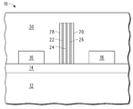
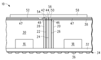
도 1에는, 캐리어(12), 테이프(14), 엘리먼트(16), 엘리먼트(18), 및 커넥션 블럭(20)을 포함하는 패키지(10)가 도시되어 있다. 캐리어(12)는 기계적 지지를 제공하기 위한 것이다. 테이프(14)는 양면으로 되어 있다. 엘리먼트(16)는 집적 회로일 수 있으며, 엘리먼트(18)도 집적 회로일 수 있다. 패시브 디바이스 혹은 개별적 반도체 디바이스와 같은 다른 유형의 엘리먼트가 위에 있거나 혹은 다른 것이 될 수 있다. 커넥션 블럭(20)은, 커넥션 블럭(20)의 길이를 따라 수직으로 운용되고 유전체(28)에 의해 둘러싸이는 도전체(22), 도전체(24), 및 도전체(26)를 갖는다. 유전체(28)는, RCP를 제조할 때에 필(fill)로서 사용되는 것과 유사하거나 혹은 그와 동일한 유기 물질인 것이 바람직하지만, 유전체(28)는 또한 세라믹과 같은 다른 물질일 수도 있다. 도전체들(22, 24, 26)에 대해서는 구리가 바람직한 물질인데, 그 이유는 구리가 비교적 높은 도전성을 가지며 비교적 가격이 낮기 때문이다. 백금, 금, 또는 은과 같은 더욱 전도성이 높은 물질이 사용될 수도 있지만, 가격이 더 비싸다. 커넥션 블럭(20)의 길이는, 마무리된(finished) RCP의 엘리먼트들을 둘러싸는 유기 층의 두께보다 약간 더 두껍게 되도록 선택된다. 이 엘리먼트들을 둘러싸는 유기 층의 통상의 두께는 약 0.65mm이지만, 이는 변동될 수 있다. 이러한 0.65mm의 경우, 커넥션 블럭(20) 및 이에 따른 도전체들(22, 24, 26)은 약 0.70mm의 길이이다. 커넥션 블럭(20)은 1mm 혹은 그 이상의 직경을 갖는 것이 바람직하다. 직경이 더 작으면 테이프(14)에 신뢰성있게 부착되기 어렵지만, 그럼에도 불구하고 몇몇 응용의 경우 이로울 수도 있다.1, a
도 2에는, 엘리먼트들(16, 18) 및 커넥션 블럭(20)을 덮는 유기 층(30)의 증착 후의 패키지(10)가 도시되어 있다. 유기 층(30)은, 커넥션 블럭(20)이 약 0.70mm인 예의 경우, 약 0.80mm가 되도록 증착될 수 있다. 유기 층(30)은 중합체 층인 것으로 간주될 수 있다.In FIG. 2, the
도 3에는, 유기 층(30) 및 커넥션 블럭(20)의 작은 부분을 그라인딩(grinding)하여 도전체들(22, 24, 26)을 노출시킨 후의 패키지(10)가 도시되어 있다. 그 후, 유기 층(30)은, 이 예에서, 0.65mm로 감소된다.3 shows a
도 4에는, 캐리어(12) 및 테이프(14)를 제거한 후의 패키지(10)가 도시되어 있다. 도 4는 또한, 도 1-3의 것과는 역전되어 있는 패키지(10)를 갖는다. 엘리먼트들(16, 18)은 패키지(10)의 상부 면 상에서 노출되어 있다. 엘리먼트(16)의 노출된 표면 및 엘리먼트(18)의 노출 표면에는, 엘리먼트들(16, 18)에 대한 컨택트들이 존재한다.4 shows the
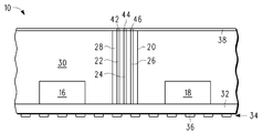
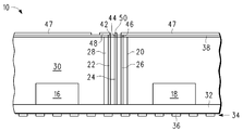
도 5에는, 커넥션 블럭(20), 엘리먼트(16), 및 엘리먼트(18)와 접촉하는 인터커넥트(32)를 형성한 후의 패키지(10)가 도시되어 있다. 인터커넥트(32)는, 비아들을 이용하여 엘리먼트들(16, 18) 및 커넥션 블럭(20)에 연결된 다수의 도전성 층들로 이루어질 수 있다. 인터커넥트(32) 상에는, 복수의 패드들(34)이 존재하는데, 이들 중 하나가 패드(36)이다. 패드들(34)은 땜납 볼들(solder balls)을 수용하기 위한 것으로 패키지(10)의 상부 면 상에 있다. 커넥션 블럭(20)은 패키지(10)의 이면 상에서 노출된다. 커넥션 블럭(20)을 가지지 않았을 수 있는 통상의 RCP에서, 프로세싱은 땜납 볼들을 제외하고 완료될 수 있다. 땜납 볼들은 이때 추가될 수도 있고 혹은 후속하는 편리한 시간에 추가될 수도 있다.In FIG. 5, the
도 6에는, 이면 상에 유전체 층(38)을 형성하고 유전체 층(38)을 통하여 비아들(42, 44, 46)을 형성한 후의 패키지(10)가 도시되어 있다. 유전체 층(38)은 유기 층(30)과 동일한 물질인 것이 바람직하지만, 다른 절연 물질일 수도 있다. 유전체 층(38)은 0.1mm 두께일 수 있다. 비아(42)는 도전체(22)와 접촉한다. 비아(44)는 도전체(24)와 접촉한다. 비아(46)는 도전체(46)와 접촉한다. 도 6은 또한 도 4 및 도 5로부터 역전된 패키지(10)를 도시한다. 패드들(34)을 갖는 면은 여전히 상부 면이라 불리우며, 유전체 층(38)을 갖는 면은 여전히 이면이라 불린다.In FIG. 6, the
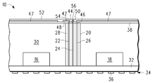
도 7에는, 유전체 층(38) 위에, 비아(40)와 접촉하는 접지 면(47), 비아(42)와 접촉하는 트레이스(48), 및 비아(44)와 접촉하는 트레이스(50)를 포함하는 패터닝된 도전성 층을 형성한 후의 패키지(10)가 도시되어 있다. 접지 면(47)은 트레이스들(48, 50)을 둘러싼다. 트레이스(48)는 비아(42)로부터 측면으로 연장되며 안정성을 위해 존재하는 것이다. 마찬가지로, 트레이스(50)는 비아(44)로부터, 트레이스(48)와는 다른 방향으로 측면으로 연장되어서, 측면 연장부가 도 7의 단면도에는 보여지지 않게 된다. 패터닝된 도전성 층은 통상의 도금 처리에 의해 제조될 수 있는데, 이 도금 처리에서는, 얇은 시드 층이 증착되고 그 후 패터닝되는 포토레지스트가 도포된다. 그 후, 도금이 행해져서, 도전성 물질, 바람직하게는 구리(다른 금속들도 또한 효과적일 수 있음)가 그 영역들 내에서 성장하게 되지만 포토레지스트에 의해 피복되지는 않는다. 포토레지스트는 제거된다. 도전성 층이 성장되지 않은 영역들 내에서 시드 층을 제거하기 위해 에치 백(etch back)이 행해진다. 접지 면(47) 및 트레이스들(48, 50)의 두께는 약 0.10mm일 수 있다.7 includes a
도 8에는, 유전체 층(52), 및 유전체 층(52)을 통과하는 비아들(54, 56)을 형성한 후의 패키지(10)가 도시되어 있다. 유전체 층(52)은, 유전체 층(38)과 동일한 재료로 이루어질 수 있다. 비아(54)는 트레이스(48)와 접촉한다. 비아(56)는 트레이스(50)와 접촉한다. 비아(56)가 도 8의 단면도에서 트레이스(50)와 접촉하는 것으로 도시되어 있지만, 비아(56)는 도시된 것보다 더 넓은 트레이스(50)의 부분 위에 위치하는 것이 바람직하다.In FIG. 8, the
도 9에는, 비아들(54, 56)과 접촉하는 안테나(58)를 형성한 후의 패키지(10)가 도시되어 있다. 접지 면(47) 및 트레이스들(48, 50)에 대해 기술된 것과 동일한 도금 기술을 이용하여 안테나(58)가 형성 및 패터닝될 수 있다. 안테나(58)는 0.200mm 두께일 수 있다. 비아들(54, 56)과 접촉하는 안테나(58)에서, 안테나는 도전체들(22, 24) 각각과 결합되어 있다. 수반될 수 있는 높은 주파수들로 인해, 비아들(54, 56)은, 도전체(22)와 결합될 안테나(58)에 대해, 안테나(58)에 충분히 밀접해 있는 경우, 안테나(58)와 실제로 접촉하여 있지 않아도 될 수 있다. 도 9의 패키지(10)는, 나중에 회로 기판 상에 장착되는 것에 더 가까운 시간에 땜납 볼들이 추가될 완료된 RCP이다.In FIG. 9, the
도 10에는, 한줄로 된 도전체들(22, 24, 26)과, 원형으로 이들을 둘러싸는 유전체(28)를 나타내는 커넥션 블럭(20)의 평면도가 도시되어 있다. 이 구성에서, 커넥션 블럭(20)은 세 개의 인라인(inline) 도전체들을 갖는 원통형이다. 도전체들(22, 24, 26)은 서로 다른 구성으로 되어 있을 수 있다. 또한, 그 형태는 원형과 다를 수 있는데, 예를 들면, 정사각형, 직사각형, 혹은 삼각형일 수 있다.10 shows a plan view of a
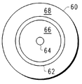
도 11에는, 외부 절연 층(68), 도전체 링(62), 내부 도전체(64), 및 도전체 링(62)과 내부 도전체(64) 사이의 절연 층을 포함하는 대안적인 커넥션 블럭(60)이 도시되어 있다. 이는, RF를 송신 및 수신하는 안테나에 결합될 때 특히 이로울 수 있는 동축선을 형성한다. 커넥션 블럭(60)은 안테나(58)에 대한 커넥션에 대하여 커넥션 블럭(20)을 대체할 수 있다. 접지 면이 여전히 바람직한 경우, 접지 면에 대한 커넥션은 다른 커넥션 블럭에 의한 것일 수 있거나, 혹은 커넥션 블럭(60)은 접지 면으로의 결합을 위해 다른 도전체 외부 링(62)을 가지도록 변경될 수 있다.In FIG. 11, an alternative connection block includes an
커넥션 블럭(20) 또는 커넥션 블럭(60)과 같은 커넥션 블럭의 구성은, 와이어 본드 머신(wire bond machines)을 이용하여 달성될 수 있다. 와이어 본드는 통상적으로 25 마이크론의 직경을 갖는다. 이들 와이어 본드들 중 세 개가 커넥션 블럭(20)의 것보다 훨씬 더 긴 원통형 몰드 내에 놓여질 수 있다. 이 몰드는, 원하는 유전체, 예를 들면 유전체(30)에 이용되는 물질로 채워진다. 이에 따라 생성된 구조체는, 그 후 약 0.070mm의 원하는 길이의 조각들로 절단된다. 유기 물질 대신에, 둘러싸는 유전체는, 세라믹과 같은 물질일 수 있다. 세라믹의 강도는 제조 프로세스에서 이로울 수 있다.The configuration of the connection block, such as the
지금까지, 인터커넥트 층, 반도체 디바이스, 제1 도전성 엘리먼트, 및 커넥터 블럭을 갖는 패키지화된 반도체 디바이스가 제공되었음을 알 것이다. 인터커넥트 층은, 중합체 층의 제1 면 위에 있다. 반도체 디바이스는, 중합체 층에 의해 적어도 세 면이 둘러싸이며, 인터커넥트 층에 결합된다. 제1 도전성 엘리먼트는 중합체 층의 제2 면 위에 있다. 제2 면은 제1 면과 반대측에 있다. 커넥터 블럭은 중합체 층 내에 있으며, 커넥터 블럭의 제1 표면으로부터 커넥터 블럭의 제2 표면으로 연장되는 적어도 하나의 전기 경로를 가지며, 인터커넥트 층을, 적어도 하나의 전기 경로를 통하여 제1 도전성 엘리먼트에 전기적으로 결합시킨다. 커넥터 블럭은 적어도 하나의 전기 경로를 둘러싸는 절연 물질을 포함할 수 있다. 커넥터 블럭은 적어도 두 개의 동축 전기 경로들을 가질 수 있다. 적어도 하나의 전기 경로는 접지 경로일 수 있으며, 제1 도전성 엘리먼트는 접지 면일 수 있다. 적어도 하나의 전기 경로는 신호 경로일 수 있으며, 제1 도전성 엘리먼트는 안테나일 수 있다. 패키지화된 반도체 디바이스는, 제2 도전성 엘리먼트 및 제2 전기 경로를 더 포함할 수 있으며, 여기서, 제2 전기 경로는 접지 경로이며, 제2 도전성 엘리먼트는 접지 면이다. 패키지화된 반도체 디바이스는 제3 전기 경로를 더 포함할 수 있는데, 여기서 제3 전기 경로는 안테나에 결합된다.Thus far, it will be appreciated that a packaged semiconductor device having an interconnect layer, a semiconductor device, a first conductive element, and a connector block has been provided. The interconnect layer is on the first side of the polymer layer. The semiconductor device is surrounded by at least three sides by a polymer layer and bonded to the interconnect layer. The first conductive element is on the second side of the polymer layer. The second face is on the opposite side to the first face. The connector block is in a polymer layer and has at least one electrical path extending from the first surface of the connector block to the second surface of the connector block and electrically connecting the interconnect layer to the first conductive element through the at least one electrical path. Combine. The connector block may comprise an insulating material surrounding at least one electrical path. The connector block may have at least two coaxial electrical paths. The at least one electrical path may be a ground path and the first conductive element may be a ground plane. At least one electrical path may be a signal path and the first conductive element may be an antenna. The packaged semiconductor device may further include a second conductive element and a second electrical path, where the second electrical path is a ground path and the second conductive element is a ground plane. The packaged semiconductor device can further include a third electrical path, where the third electrical path is coupled to the antenna.
또한, 패키지화된 반도체 디바이스를 형성하기 위한 방법이 제공된다. 이 방법은 중합체 층에 의해 반도체 디바이스의 적어도 세 개의 면을 둘러싸는 단계를 포함한다. 이 방법은, 중합체 층의 제1 면과, 반도체 디바이스 상에 인터커넥트 층을 형성하는 단계를 더 포함하며, 여기서 반도체 디바이스는 인터커넥트 층에 결합된다. 이 방법은, 중합체 층의 제2 면 위에 도전성 엘리먼트를 형성하는 단계를 더 포함하며, 여기서 제2 면은 제1 면과 반대측에 있다. 이 방법은, 적어도 하나의 전기 경로를 갖는, 중합체 층 내의 커넥터 블럭을 통해 인터커넥트 층을 도전성 엘리먼트에 전기적으로 결합시키는 단계를 더 포함한다. 제2 면 상에 도전성 엘리먼트를 형성하는 단계는, 도전성 물질을 도금하여서 안테나를 형성하는 단계를 포함할 수 있다. 둘러싸는 단계는, 반도체 디바이스를 일시적 지지 구조체에 부착시키는 단계, 반도체 디바이스 상에 중합체 층을 형성하는 단계, 및 중합체 층을 형성한 후 일시적 지지 구조체를 제거하는 단계를 포함할 수 있다. 전기적으로 결합시키는 단계는, 중합체 층을 형성하기 전에 일시적 지지 구조체에 커넥터 블럭을 부착시키는 단계, 중합체 층의 일부를 제거하여서 커넥터 블럭의 표면을 노출시키는 단계, 중합체 층의 제1 면 상에 인터커넥트 층을 형성하는 동안 커넥터 블럭의 표면 상에 인터커넥트 층을 형성하는 단계를 포함할 수 있다. 이 방법은, 커넥터 블럭의 표면 위에 유전체 층을 증착하는 단계, 및 유전체 층 내에 비아를 형성하는 단계를 더 포함할 수 있으며, 여기서 비아는 커넥터 블럭 및 도전성 엘리먼트에 전기적으로 결합된다. 적어도 하나의 전기 경로는, 접지 경로 및 신호 경로로 구성된 그룹으로부터 선택될 수 있다. 제1 도전성 엘리먼트는, 접지 면 및 안테나로 구성된 그룹으로부터 선택될 수 있다. 적어도 하나의 전기 경로는 적어도 두 개의 동축 전기 경로들을 포함할 수 있다.Also provided are methods for forming a packaged semiconductor device. The method includes enclosing at least three sides of the semiconductor device by a polymer layer. The method further includes forming an interconnect layer on the first side of the polymer layer and on the semiconductor device, where the semiconductor device is coupled to the interconnect layer. The method further includes forming a conductive element over the second side of the polymer layer, where the second side is opposite the first side. The method further includes electrically coupling the interconnect layer to the conductive element through a connector block in the polymer layer having at least one electrical path. Forming the conductive element on the second surface may include plating the conductive material to form the antenna. Surrounding may include attaching the semiconductor device to the temporary support structure, forming a polymer layer on the semiconductor device, and removing the temporary support structure after forming the polymer layer. Electrically bonding includes attaching the connector block to the temporary support structure prior to forming the polymer layer, removing a portion of the polymer layer to expose the surface of the connector block, interconnect layer on the first side of the polymer layer. Forming an interconnect layer on the surface of the connector block while forming the interconnect. The method may further include depositing a dielectric layer over the surface of the connector block, and forming a via in the dielectric layer, wherein the via is electrically coupled to the connector block and the conductive element. The at least one electrical path may be selected from the group consisting of a ground path and a signal path. The first conductive element may be selected from the group consisting of a ground plane and an antenna. At least one electrical path may comprise at least two coaxial electrical paths.
패키지화된 반도체 디바이스를 형성하기 위한 방법이 또한 기술되어 있다. 이 방법은 반도체 디바이스를 일시적 지지 구조체에 부착하는 단계를 포함한다. 이 방법은 커넥터 블럭을 일시적 지지 구조체에 부착하는 단계를 더 포함하는데, 여기서 커넥터 블럭은 적어도 하나의 전기 경로를 갖는다. 이 방법은 커넥터 블럭 및 반도체 디바이스 위에 인캡슐런트(encapsulant)를 형성하는 단계를 더 포함한다. 이 방법은, 인캡슐런트의 일부를 제거하여서 커넥터 블럭의 상부 표면을 노출시키는 단계를 더 포함한다. 이 방법은, 커넥터 블럭의 상부 표면에 전기적으로 결합된 인터커넥트 층을 형성하는 단계를 더 포함한다. 이 방법은, 일시적 지지 구조체를 제거하여서 커넥터 블럭의 하부 표면을 노출시키는 단계를 더 포함한다. 이 방법은 유형의 엘리먼트(tangible element)를 커넥터 블럭의 하부 표면에 전기적으로 결합시키는 단계를 더 포함한다. 유형의 엘리먼트를 커넥터 블럭의 하부 표면에 전기적으로 결합시키는 단계는, 도전성 물질을 도금하여서 안테나를 형성하는 단계를 포함할 수 있다. 유형의 엘리먼트를 커넥터 블럭의 하부 표면에 전기적으로 결합시키는 단계는, 커넥터 블럭의 하부 표면 위에 유전체 층을 증착시키는 단계, 및 유전체 층 내에 비아를 형성하는 단계를 더 포함할 수 있으며, 여기서 비아는 커넥터 블럭 및 안테나에 전기적으로 결합된다. 인캡슐런트의 일부를 제거하여서 커넥터 블럭의 상부 표면을 노출시키는 단계는 인캡슐런트를 그라인딩하는 단계를 포함할 수 있다. 일시적 지지 구조체는, 테이프 및 캐리어로 구성된 그룹으로부터 선택될 수 있다. 커넥터 블럭은 적어도 두 개의 동축 전기 경로들을 가질 수 있다.A method for forming a packaged semiconductor device is also described. The method includes attaching a semiconductor device to a temporary support structure. The method further includes attaching the connector block to the temporary support structure, wherein the connector block has at least one electrical path. The method further includes forming an encapsulant over the connector block and the semiconductor device. The method further includes exposing a top surface of the connector block by removing a portion of the encapsulant. The method further includes forming an interconnect layer electrically coupled to the top surface of the connector block. The method further includes exposing the bottom surface of the connector block by removing the temporary support structure. The method further includes electrically coupling a tangible element to the bottom surface of the connector block. Electrically coupling the tangible element to the bottom surface of the connector block may include plating the conductive material to form the antenna. Electrically coupling the tangible element to the bottom surface of the connector block may further include depositing a dielectric layer over the bottom surface of the connector block, and forming a via in the dielectric layer, wherein the via is a connector. It is electrically coupled to the block and the antenna. Exposing a portion of the encapsulant to expose the top surface of the connector block may include grinding the encapsulant. The temporary support structure may be selected from the group consisting of a tape and a carrier. The connector block may have at least two coaxial electrical paths.
또한, 명세서 및 특허청구범위에서, "앞(front)", "뒤(back)", "상부(top)", "하부(bottom)", "위(over)", "아래(under)" 등과 같은 용어(있는 경우에 한함)는, 설명을 위한 것으로, 반드시 영구적인 상대적인 위치를 기술하는 것은 아니다. 이와 같이 사용된 용어들은 적절한 상황하에서 상호교환가능하여서, 본원에 기술되는 본 발명의 실시예들이, 예를 들어 본원에 예시되거나 혹은 설명된 것과는 다른 방위로 동작할 수 있게 됨을 알 것이다.Also, in the specification and claims, "front", "back", "top", "bottom", "over", "under" Terms such as the like (if any) are for illustration only and do not necessarily describe permanent relative positions. It will be appreciated that the terms used as such are interchangeable under appropriate circumstances, such that embodiments of the invention described herein may operate in a different orientation than, for example, those illustrated or described herein.
본 발명은 본원에서 특정 실시예들을 참조하여 설명되지만, 이하의 특허청구범위에 제시된 바와 같은 본 발명의 범주로부터 벗어나지 않고 다양한 수정 및 변경이 행해질 수 있다. 예를 들면, 유전 층(38)이, 인터커넥트 층(32) 후에 형성되는 것으로 도시되어 있지만, 유전 층(38)은 인터커넥트 층(32)이 형성되기 전에 증착될 수도 있다. 또한, 패터닝된 금속 층들을 형성하기 위한 방법으로서 도금이 기술되었지만, 그 밖의 다른 증착 기술들이 이용될 수도 있다. 예를 들면, 금속은 스퍼터링된 후, 에치에 의해 패터닝될 수 있다. 따라서, 본 명세서 및 도면들은 제한적인 의미가 아니라 예시적인 것으로 간주되어야 하며, 이러한 모든 변형들은 본 발명의 범주 내에 포함되는 것으로 의도된다. 특정 실시예들과 관련하여 본원에 기술된 임의의 이점들, 이익들, 문제들에 대한 해법들은, 임의의 청구항들 혹은 모든 청구항들의 결정적이거나, 요구되거나, 혹은 필수적인 특성 또는 엘리먼트인 것으로 이해되어서는 않된다.Although the invention has been described herein with reference to specific embodiments, various modifications and changes may be made without departing from the scope of the invention as set forth in the claims below. For example, although
본원에서 사용되는 "결합된(coupled)"이라는 용어는, 직접적인 결합 혹은 기계적 결합으로 제한되어서는 않된다.As used herein, the term "coupled" should not be limited to direct coupling or mechanical coupling.
또한, 본원에서 사용되는 "하나(a 또는 an)"라는 용어는, 하나 또는 하나 이상으로 정의된다. 또한, 특허청구범위에서 "적어도 하나(at least one)" 및 "하나 이상(one or more)"과 같은 도입 문구의 사용은, 동일한 청구항이 "하나 이상" 혹은 "적어도 하나"와 같은 도입 문구 및 부정관사("a" 또는 "an")를 포함하고 있을 때에도, 부정 관사("a" 또는 "an")에 의한 다른 청구항 엘리먼트의 도입이, 이러한 엘리먼트 하나만을 포함하고 있는 본 발명의 이러한 도입된 청구항 엘리먼트를 포함하는 임의의 특정 청구항을 제한하는 것을 암시하고 있는 것으로 해석하여서는 않된다. 이는, 정관사(definite articles)의 사용에 대해서는 적용된다.Also, as used herein, the term "a" or "an" is defined as one or more than one. Also, in the claims, the use of introductory phrases such as "at least one" and "one or more" shall be construed as incorporating phrases such as "one or more" or "at least one" in the same claim. Even when an indefinite article "a" or "an" is included, the introduction of another claim element by the indefinite article "a" or "an" is such an introduction of the present invention that includes only one such element. It should not be construed as implying any limitation to any particular claim, including any claim elements. This applies to the use of definite articles.
달리 진술되지 않는 한, "제1" 및 "제2"와 같은 용어들은, 이러한 용어들이 기술하는 엘리먼트들을 임의로 구별하는데에 이용된다. 따라서, 이들 용어들은 이러한 엘리먼트들의 시간적 혹은 그 밖의 다른 우선순위를 가리키는 것을 반드시 의도하는 것은 아니다.Unless stated otherwise, terms such as “first” and “second” are used to arbitrarily distinguish elements described by such terms. Accordingly, these terms are not necessarily intended to indicate the temporal or other priority of these elements.
Claims (20)
중합체 층의 제1 면(side) 위의 인터커넥트 층(interconnect layer);
상기 중합체 층에 의해 적어도 세 개의 면이 둘러싸이며 상기 인터커넥트 층에 결합된 반도체 디바이스;
상기 중합체 층의 제2 면 위의 제1 도전성 엘리먼트 - 상기 제2 면은 상기 제1 면과 반대측에 있음 -; 및
상기 중합체 층 내의 커넥터 블럭(connector block) - 상기 커넥터 블럭은, 상기 커넥터 블럭의 제1 표면(surface)으로부터 상기 커넥터 블럭의 제2 표면으로 연장되는 적어도 하나의 전기 경로를 가지며, 상기 적어도 하나의 전기 경로를 통하여 상기 인터커넥트 층을 상기 제1 도전성 엘리먼트에 전기적으로 결합시킴 -
을 포함하는 패키지화된 반도체 디바이스.A packaged semiconductor device,
An interconnect layer on the first side of the polymer layer;
A semiconductor device surrounded by at least three sides by the polymer layer and bonded to the interconnect layer;
A first conductive element on a second side of the polymer layer, wherein the second side is opposite the first side; And
Connector block in the polymer layer, the connector block having at least one electrical path extending from a first surface of the connector block to a second surface of the connector block, wherein the at least one electrical Electrically coupling the interconnect layer to the first conductive element via a path;
Packaged semiconductor device comprising a.
상기 커넥터 블럭은 상기 적어도 하나의 전기 경로를 둘러싸는 절연 물질을 포함하는, 패키지화된 반도체 디바이스.The method of claim 1,
And the connector block comprises an insulating material surrounding the at least one electrical path.
상기 커넥터 블럭은 적어도 두 개의 동축 전기 경로들을 가지는, 패키지화된 반도체 디바이스.The method of claim 1,
And the connector block has at least two coaxial electrical paths.
상기 적어도 하나의 전기 경로는 접지 경로이며, 상기 제1 도전성 엘리먼트는 접지 면(ground plane)인, 패키지화된 반도체 디바이스.The method of claim 1,
Wherein the at least one electrical path is a ground path and the first conductive element is a ground plane.
상기 적어도 하나의 전기 경로는 신호 경로이며, 상기 제1 도전성 엘리먼트는 안테나인, 패키지화된 반도체 디바이스.The method of claim 1,
The at least one electrical path is a signal path and the first conductive element is an antenna.
제2 도전성 엘리먼트 및 제2 전기 경로를 더 포함하며, 상기 제2 전기 경로는 접지 경로이며, 상기 제2 도전성 엘리먼트는 접지 면인, 패키지화된 반도체 디바이스.The method of claim 5,
And a second conductive element and a second electrical path, wherein the second electrical path is a ground path and the second conductive element is a ground plane.
제3 전기 경로를 더 포함하며, 상기 제3 전기 경로는 상기 안테나에 결합되는, 패키지화된 반도체 디바이스.The method of claim 6,
And a third electrical path, the third electrical path coupled to the antenna.
중합체 층에 의해 반도체 디바이스의 적어도 세 개의 면을 둘러싸는 단계;
상기 중합체 층의 제1 면과 상기 반도체 디바이스 위에 인터커넥트 층을 형성하는 단계 - 상기 반도체 디바이스는 상기 인터커넥트 층에 결합됨 -;
상기 중합체 층의 제2 면 위에 도전성 엘리먼트를 형성하는 단계 - 상기 제2 면은 상기 제1 면과 반대측에 있음 -; 및
상기 중합체 층 내의 커넥터 블럭을 통하여 상기 인터커넥트 층을 상기 도전성 엘리먼트에 전기적으로 결합시키는 단계 - 상기 커넥터 블럭은 적어도 하나의 전기 경로를 가짐 -
를 포함하는 패키지화된 반도체 디바이스 형성 방법.A method for forming a packaged semiconductor device,
Enclosing at least three sides of the semiconductor device by the polymer layer;
Forming an interconnect layer over the first side of the polymer layer and the semiconductor device, the semiconductor device being coupled to the interconnect layer;
Forming a conductive element over a second side of the polymer layer, the second side being opposite the first side; And
Electrically coupling the interconnect layer to the conductive element through a connector block in the polymer layer, the connector block having at least one electrical path
Packaged semiconductor device forming method comprising a.
상기 제2 면 위에 도전성 엘리먼트를 형성하는 단계는, 도전성 물질을 도금하여 안테나를 형성하는 단계를 포함하는, 패키지화된 반도체 디바이스 형성 방법.The method of claim 8,
Forming a conductive element on the second surface comprises plating an conductive material to form an antenna.
상기 중합체 층에 의해 반도체 디바이스의 적어도 세 개의 면을 둘러싸는 단계는,
반도체 디바이스를 일시적 지지 구조체에 부착하는 단계;
상기 반도체 디바이스 위에 상기 중합체 층을 형성하는 단계; 및
상기 중합체 층의 형성 후에 상기 일시적 지지 구조체를 제거하는 단계
를 포함하며,
상기 인터커넥트 층을 전기적으로 결합시키는 단계는,
상기 중합체 층을 형성하기 전에 상기 커넥터 블럭을 상기 일시적 지지 구조체에 부착시키는 단계;
상기 중합체 층의 일부를 제거하여서 상기 커넥터 블럭의 표면을 노출시키는 단계; 및
상기 중합체 층의 상기 제1 면 위에 상기 인터커넥트 층을 형성하는 동안, 상기 커넥터 블럭의 표면 위에 상기 인터커넥트 층을 형성하는 단계
를 포함하는, 패키지화된 반도체 디바이스 형성 방법.The method of claim 8,
Surrounding at least three sides of the semiconductor device by the polymer layer,
Attaching the semiconductor device to the temporary support structure;
Forming the polymer layer over the semiconductor device; And
Removing the temporary support structure after formation of the polymer layer
Including;
Electrically coupling the interconnect layer,
Attaching the connector block to the temporary support structure prior to forming the polymer layer;
Removing a portion of the polymer layer to expose a surface of the connector block; And
While forming the interconnect layer on the first side of the polymer layer, forming the interconnect layer on the surface of the connector block
Comprising a packaged semiconductor device.
상기 커넥터 블럭의 표면 위에 유전체 층을 증착하는 단계; 및
상기 유전체 층 내에 비아를 형성하는 단계 - 상기 비아는 상기 커넥터 블럭 및 상기 도전성 엘리먼트에 전기적으로 결합됨 -
를 더 포함하는, 패키지화된 반도체 디바이스 형성 방법.The method of claim 10,
Depositing a dielectric layer over the surface of the connector block; And
Forming a via in the dielectric layer, wherein the via is electrically coupled to the connector block and the conductive element
Further comprising a packaged semiconductor device.
상기 적어도 하나의 전기 경로는 접지 경로 및 신호 경로로 구성된 그룹으로부터 선택되는, 패키지화된 반도체 디바이스 형성 방법.The method of claim 8,
Wherein the at least one electrical path is selected from the group consisting of a ground path and a signal path.
상기 제1 도전성 엘리먼트는, 접지 면 및 안테나로 구성된 그룹으로부터 선택되는, 패키지화된 반도체 디바이스 형성 방법.The method of claim 8,
And wherein the first conductive element is selected from the group consisting of a ground plane and an antenna.
상기 적어도 하나의 전기 경로는 적어도 두 개의 동축 전기 경로들을 포함하는, 패키지화된 반도체 디바이스 형성 방법.The method of claim 8,
And the at least one electrical path comprises at least two coaxial electrical paths.
반도체 디바이스를 일시적 지지 구조체에 부착하는 단계;
상기 일시적 지지 구조체에 커넥터 블럭을 부착하는 단계 - 상기 커넥터 블럭은 적어도 하나의 전기 경로를 가짐 -;
상기 커넥터 블럭 및 상기 반도체 디바이스 위에 인캡슐런트(encapsulant)를 형성하는 단계;
상기 인캡슐런트의 일부를 제거하여서 상기 커넥터 블럭의 상부 표면(top surface)을 노출시키는 단계;
상기 커넥터 블럭의 상부 표면에 전기적으로 결합되는 인터커넥트 층을 형성하는 단계;
상기 일시적 지지 구조체를 제거하여서 상기 커넥터 블럭의 하부 표면(bottom surface)을 노출시키는 단계; 및
상기 커넥터 블럭의 하부 표면에 유형의 엘리먼트(tangible element)를 전기적으로 결합시키는 단계
를 포함하는 패키지화된 반도체 디바이스 형성 방법.A method of forming a packaged semiconductor device,
Attaching the semiconductor device to the temporary support structure;
Attaching a connector block to the temporary support structure, the connector block having at least one electrical path;
Forming an encapsulant over the connector block and the semiconductor device;
Removing a portion of the encapsulant to expose a top surface of the connector block;
Forming an interconnect layer electrically coupled to a top surface of the connector block;
Removing the temporary support structure to expose a bottom surface of the connector block; And
Electrically coupling a tangible element to the bottom surface of the connector block
Packaged semiconductor device forming method comprising a.
상기 커넥터 블럭의 하부 표면에 유형의 엘리먼트를 전기적으로 결합시키는 단계는, 도전성 물질을 도금하여서 안테나를 형성하는 단계를 포함하는, 패키지화된 반도체 디바이스 형성 방법.16. The method of claim 15,
Electrically coupling a tangible element to a bottom surface of the connector block comprises plating an electrically conductive material to form an antenna.
상기 커넥터 블럭의 하부 표면에 유형의 엘리먼트를 전기적으로 결합시키는 단계는,
상기 커넥터 블럭의 하부 표면 위에 유전체 층을 증착시키는 단계; 및
상기 유전체 층 내에 비아를 형성하는 단계 - 상기 비아는 상기 커넥터 블럭 및 상기 안테나에 전기적으로 결합됨 -
를 더 포함하는, 패키지화된 반도체 디바이스 형성 방법.The method of claim 16,
Electrically coupling an element of type to a lower surface of the connector block,
Depositing a dielectric layer over the bottom surface of the connector block; And
Forming a via in the dielectric layer, the via electrically coupled to the connector block and the antenna;
Further comprising a packaged semiconductor device.
상기 인캡슐런트의 일부를 제거하여서 상기 커넥터 블럭의 상부 표면을 노출시키는 단계는, 상기 인캡슐런트를 그라인딩(grinding)하는 단계를 포함하는, 패키지화된 반도체 디바이스 형성 방법.16. The method of claim 15,
Exposing the upper surface of the connector block by removing a portion of the encapsulant, grinding the encapsulant.
상기 일시적 지지 구조체는, 테이프 및 캐리어로 구성된 그룹으로부터 선택되는, 패키지화된 반도체 디바이스 형성 방법.16. The method of claim 15,
And wherein the temporary support structure is selected from the group consisting of a tape and a carrier.
상기 커넥터 블럭은 적어도 두 개의 동축 전기 경로를 갖는, 패키지화된 반도체 디바이스 형성 방법.16. The method of claim 15,
And the connector block has at least two coaxial electrical paths.
Applications Claiming Priority (2)
| Application Number | Priority Date | Filing Date | Title |
|---|---|---|---|
| US11/846,874 | 2007-08-29 | ||
| US11/846,874 US7838420B2 (en) | 2007-08-29 | 2007-08-29 | Method for forming a packaged semiconductor device |
Publications (1)
| Publication Number | Publication Date |
|---|---|
| KR20100065305A true KR20100065305A (en) | 2010-06-16 |
Family
ID=40406108
Family Applications (1)
| Application Number | Title | Priority Date | Filing Date |
|---|---|---|---|
| KR1020107004435A KR20100065305A (en) | 2007-08-29 | 2008-07-09 | Interconnect in a multi-element package |
Country Status (7)
| Country | Link |
|---|---|
| US (1) | US7838420B2 (en) |
| EP (1) | EP2195840A4 (en) |
| JP (1) | JP5397962B2 (en) |
| KR (1) | KR20100065305A (en) |
| CN (1) | CN101790788A (en) |
| TW (1) | TWI451551B (en) |
| WO (1) | WO2009032398A1 (en) |
Families Citing this family (21)
| Publication number | Priority date | Publication date | Assignee | Title |
|---|---|---|---|---|
| JP2010245107A (en) * | 2009-04-01 | 2010-10-28 | Shinko Electric Ind Co Ltd | Semiconductor apparatus and method of manufacturing the same |
| US8407890B2 (en) * | 2010-01-25 | 2013-04-02 | Freescale Semiconductor Inc. | Method of manufacting an electronic device module with integrated antenna structure |
| US8916421B2 (en) | 2011-08-31 | 2014-12-23 | Freescale Semiconductor, Inc. | Semiconductor device packaging having pre-encapsulation through via formation using lead frames with attached signal conduits |
| US9142502B2 (en) | 2011-08-31 | 2015-09-22 | Zhiwei Gong | Semiconductor device packaging having pre-encapsulation through via formation using drop-in signal conduits |
| US8597983B2 (en) | 2011-11-18 | 2013-12-03 | Freescale Semiconductor, Inc. | Semiconductor device packaging having substrate with pre-encapsulation through via formation |
| JP5834907B2 (en) * | 2011-12-28 | 2015-12-24 | 富士通株式会社 | Semiconductor device, semiconductor device manufacturing method, and electronic device |
| US9837303B2 (en) | 2012-03-23 | 2017-12-05 | STATS ChipPAC Pte. Ltd. | Semiconductor method and device of forming a fan-out device with PWB vertical interconnect units |
| US8810024B2 (en) * | 2012-03-23 | 2014-08-19 | Stats Chippac Ltd. | Semiconductor method and device of forming a fan-out PoP device with PWB vertical interconnect units |
| US9842798B2 (en) | 2012-03-23 | 2017-12-12 | STATS ChipPAC Pte. Ltd. | Semiconductor device and method of forming a PoP device with embedded vertical interconnect units |
| US10049964B2 (en) | 2012-03-23 | 2018-08-14 | STATS ChipPAC Pte. Ltd. | Semiconductor device and method of forming a fan-out PoP device with PWB vertical interconnect units |
| CN103311141B (en) * | 2013-07-05 | 2016-01-20 | 北京理工大学 | A kind of manufacture method of coaxial vertical interconnection conductor |
| US8822268B1 (en) | 2013-07-17 | 2014-09-02 | Freescale Semiconductor, Inc. | Redistributed chip packages containing multiple components and methods for the fabrication thereof |
| US9362234B2 (en) | 2014-01-07 | 2016-06-07 | Freescale Semiconductor, Inc. | Shielded device packages having antennas and related fabrication methods |
| US10354958B2 (en) | 2014-10-01 | 2019-07-16 | Nxp Usa, Inc. | Through package circuit in fan-out wafer level package |
| US9666930B2 (en) | 2014-10-23 | 2017-05-30 | Nxp Usa, Inc. | Interface between a semiconductor die and a waveguide, where the interface is covered by a molding compound |
| TWI652775B (en) | 2016-01-11 | 2019-03-01 | 矽品精密工業股份有限公司 | Electronic package |
| US10236260B2 (en) | 2016-06-30 | 2019-03-19 | Nxp Usa, Inc. | Shielded package with integrated antenna |
| CN111034376B (en) * | 2017-08-21 | 2023-02-21 | 株式会社村田制作所 | Method for manufacturing electronic component and electronic component |
| US11557565B2 (en) | 2020-10-06 | 2023-01-17 | Nxp Usa, Inc. | Semiconductor device assembly and method therefor |
| US11502054B2 (en) | 2020-11-11 | 2022-11-15 | Nxp Usa, Inc. | Semiconductor device assembly and method therefor |
| US20240088068A1 (en) * | 2022-09-08 | 2024-03-14 | Nxp Usa, Inc. | Semiconductor device with through package via and method therefor |
Family Cites Families (26)
| Publication number | Priority date | Publication date | Assignee | Title |
|---|---|---|---|---|
| JPS56115553A (en) * | 1980-02-18 | 1981-09-10 | Fujitsu Ltd | Method of mounting integrated circuit |
| JPH10303363A (en) * | 1997-04-30 | 1998-11-13 | Sony Corp | Electronic component and manufacture therefor |
| US5949030A (en) * | 1997-11-14 | 1999-09-07 | International Business Machines Corporation | Vias and method for making the same in organic board and chip carriers |
| US6054389A (en) * | 1997-12-29 | 2000-04-25 | Vanguard International Semiconductor Corporation | Method of forming metal conducting pillars |
| US6081989A (en) * | 1998-04-30 | 2000-07-04 | Lockheed Martin Corporation | Fabrication of circuit modules with a transmission line |
| JP2000252407A (en) * | 1999-03-04 | 2000-09-14 | Hitachi Ltd | Multichip module |
| JP2001094034A (en) * | 1999-09-27 | 2001-04-06 | Nec Eng Ltd | Hybrid ic package |
| US6538210B2 (en) | 1999-12-20 | 2003-03-25 | Matsushita Electric Industrial Co., Ltd. | Circuit component built-in module, radio device having the same, and method for producing the same |
| US6444576B1 (en) | 2000-06-16 | 2002-09-03 | Chartered Semiconductor Manufacturing, Ltd. | Three dimensional IC package module |
| JP2002343927A (en) * | 2000-07-12 | 2002-11-29 | Hitachi Maxell Ltd | Semiconductor module and manufacturing method therefor |
| US7190080B1 (en) * | 2000-10-13 | 2007-03-13 | Bridge Semiconductor Corporation | Semiconductor chip assembly with embedded metal pillar |
| JP2002184934A (en) * | 2000-12-13 | 2002-06-28 | Shinko Electric Ind Co Ltd | Semiconductor device and manufacturing method thereof |
| US6593644B2 (en) | 2001-04-19 | 2003-07-15 | International Business Machines Corporation | System of a package fabricated on a semiconductor or dielectric wafer with wiring on one face, vias extending through the wafer, and external connections on the opposing face |
| JP2003188340A (en) * | 2001-12-19 | 2003-07-04 | Matsushita Electric Ind Co Ltd | Part incorporating module and its manufacturing method |
| US6753600B1 (en) | 2003-01-28 | 2004-06-22 | Thin Film Module, Inc. | Structure of a substrate for a high density semiconductor package |
| JP4141857B2 (en) * | 2003-02-18 | 2008-08-27 | 日立マクセル株式会社 | Semiconductor device |
| US6838776B2 (en) * | 2003-04-18 | 2005-01-04 | Freescale Semiconductor, Inc. | Circuit device with at least partial packaging and method for forming |
| US6921975B2 (en) * | 2003-04-18 | 2005-07-26 | Freescale Semiconductor, Inc. | Circuit device with at least partial packaging, exposed active surface and a voltage reference plane |
| JP2004327641A (en) * | 2003-04-24 | 2004-11-18 | Tdk Corp | Electronic component module |
| DE10320646A1 (en) | 2003-05-07 | 2004-09-16 | Infineon Technologies Ag | Electronic component, typically integrated circuit, system support and manufacturing method, with support containing component positions in lines and columns, starting with coating auxiliary support with photosensitive layer |
| JP2005033141A (en) * | 2003-07-11 | 2005-02-03 | Sony Corp | Semiconductor device, its manufacturing method, false wafer, its manufacturing method, and packaging structure of semiconductor device |
| US7369718B2 (en) | 2004-01-23 | 2008-05-06 | Intel Corporation | Package substrate pattern to accommodate optical waveguide |
| US20050167797A1 (en) | 2004-01-29 | 2005-08-04 | Advanpack Solutions Pte Ltd | Structure package |
| JP4615962B2 (en) * | 2004-10-22 | 2011-01-19 | ルネサスエレクトロニクス株式会社 | Semiconductor device |
| US7476918B2 (en) * | 2004-11-22 | 2009-01-13 | Panasonic Corporation | Semiconductor integrated circuit device and vehicle-mounted radar system using the same |
| JP4766049B2 (en) * | 2005-09-20 | 2011-09-07 | 株式会社村田製作所 | Manufacturing method of component built-in module and component built-in module |
-
2007
- 2007-08-29 US US11/846,874 patent/US7838420B2/en active Active
-
2008
- 2008-07-09 CN CN200880104602.4A patent/CN101790788A/en active Pending
- 2008-07-09 JP JP2010522993A patent/JP5397962B2/en active Active
- 2008-07-09 WO PCT/US2008/069516 patent/WO2009032398A1/en active Application Filing
- 2008-07-09 KR KR1020107004435A patent/KR20100065305A/en not_active Application Discontinuation
- 2008-07-09 EP EP08781552A patent/EP2195840A4/en not_active Ceased
- 2008-07-15 TW TW097126735A patent/TWI451551B/en active
Also Published As
| Publication number | Publication date |
|---|---|
| JP5397962B2 (en) | 2014-01-22 |
| EP2195840A1 (en) | 2010-06-16 |
| US7838420B2 (en) | 2010-11-23 |
| EP2195840A4 (en) | 2011-01-19 |
| TWI451551B (en) | 2014-09-01 |
| US20090057849A1 (en) | 2009-03-05 |
| JP2010538463A (en) | 2010-12-09 |
| WO2009032398A1 (en) | 2009-03-12 |
| CN101790788A (en) | 2010-07-28 |
| TW200913206A (en) | 2009-03-16 |
Similar Documents
| Publication | Publication Date | Title |
|---|---|---|
| US7838420B2 (en) | Method for forming a packaged semiconductor device | |
| US8232657B2 (en) | Packaged semiconductor assemblies and methods for manufacturing such assemblies | |
| CN107093598A (en) | Semiconductor device including antenna | |
| TW200828523A (en) | Multi-component package with both top and bottom side connection pads for three-dimensional packaging | |
| US20230343664A1 (en) | Electronic package and manufacturing method thereof | |
| US20180053753A1 (en) | Stackable molded packages and methods of manufacture thereof | |
| CN111933591A (en) | Fan-out type electromagnetic shielding packaging structure and packaging method | |
| US6790760B1 (en) | Method of manufacturing an integrated circuit package | |
| US6465882B1 (en) | Integrated circuit package having partially exposed conductive layer | |
| US8283780B2 (en) | Surface mount semiconductor device | |
| KR20160020566A (en) | Method of forming a microelectronic assembly by plating metal connectors after assemblying first and second components and corresponding device | |
| CN102683298A (en) | Package without carrier and manufacturing method thereof | |
| US20150084171A1 (en) | No-lead semiconductor package and method of manufacturing the same | |
| KR102058247B1 (en) | Semiconductor Package of using the Printed Circuit Board | |
| US10756005B2 (en) | Semiconductor device, corresponding circuit and method | |
| US9786515B1 (en) | Semiconductor device package and methods of manufacture thereof | |
| KR101659354B1 (en) | Semiconductor package and method for manufacturing the same | |
| US20240014114A1 (en) | Device package substrate structure and method therefor | |
| KR102040171B1 (en) | Semiconductor Package of using the Printed Circuit Board | |
| CA2915410C (en) | Mixed impedance bond wire connections and method of making the same | |
| KR20230019926A (en) | Semiconductor device and manufacturing method of the semiconductor device | |
| CN112204719A (en) | System and method for wafer level fabrication of devices with planar grid array interfaces |
Legal Events
| Date | Code | Title | Description |
|---|---|---|---|
| WITN | Application deemed withdrawn, e.g. because no request for examination was filed or no examination fee was paid |