KR20090015136A - 동기 회로에서 발진을 감소시키기 위한 방법 및 장치 - Google Patents
동기 회로에서 발진을 감소시키기 위한 방법 및 장치 Download PDFInfo
- Publication number
- KR20090015136A KR20090015136A KR1020087031337A KR20087031337A KR20090015136A KR 20090015136 A KR20090015136 A KR 20090015136A KR 1020087031337 A KR1020087031337 A KR 1020087031337A KR 20087031337 A KR20087031337 A KR 20087031337A KR 20090015136 A KR20090015136 A KR 20090015136A
- Authority
- KR
- South Korea
- Prior art keywords
- filter
- output
- delay
- oscillation
- input
- Prior art date
Links
- 230000010355 oscillation Effects 0.000 title claims abstract description 129
- 238000000034 method Methods 0.000 title claims abstract description 32
- 230000001360 synchronised effect Effects 0.000 title description 15
- 238000001914 filtration Methods 0.000 claims abstract description 42
- 230000004044 response Effects 0.000 claims abstract description 8
- 230000015654 memory Effects 0.000 claims description 22
- 238000009826 distribution Methods 0.000 claims description 8
- 239000004065 semiconductor Substances 0.000 claims description 6
- 230000007704 transition Effects 0.000 claims description 6
- 238000012935 Averaging Methods 0.000 claims description 5
- 238000009825 accumulation Methods 0.000 claims 2
- 230000008859 change Effects 0.000 description 13
- 238000010586 diagram Methods 0.000 description 9
- 239000000872 buffer Substances 0.000 description 8
- 230000001934 delay Effects 0.000 description 5
- 230000003111 delayed effect Effects 0.000 description 5
- 239000000758 substrate Substances 0.000 description 5
- 238000013461 design Methods 0.000 description 4
- 238000003491 array Methods 0.000 description 3
- 238000001514 detection method Methods 0.000 description 3
- 230000006870 function Effects 0.000 description 3
- 230000001629 suppression Effects 0.000 description 3
- XEEYBQQBJWHFJM-UHFFFAOYSA-N Iron Chemical compound [Fe] XEEYBQQBJWHFJM-UHFFFAOYSA-N 0.000 description 2
- 230000003139 buffering effect Effects 0.000 description 2
- 238000005516 engineering process Methods 0.000 description 2
- 230000002093 peripheral effect Effects 0.000 description 2
- 238000012545 processing Methods 0.000 description 2
- 238000000742 single-metal deposition Methods 0.000 description 2
- JBRZTFJDHDCESZ-UHFFFAOYSA-N AsGa Chemical compound [As]#[Ga] JBRZTFJDHDCESZ-UHFFFAOYSA-N 0.000 description 1
- 229910001218 Gallium arsenide Inorganic materials 0.000 description 1
- GPXJNWSHGFTCBW-UHFFFAOYSA-N Indium phosphide Chemical compound [In]#P GPXJNWSHGFTCBW-UHFFFAOYSA-N 0.000 description 1
- XUIMIQQOPSSXEZ-UHFFFAOYSA-N Silicon Chemical compound [Si] XUIMIQQOPSSXEZ-UHFFFAOYSA-N 0.000 description 1
- 238000007792 addition Methods 0.000 description 1
- 229910052782 aluminium Inorganic materials 0.000 description 1
- XAGFODPZIPBFFR-UHFFFAOYSA-N aluminium Chemical compound [Al] XAGFODPZIPBFFR-UHFFFAOYSA-N 0.000 description 1
- 238000004458 analytical method Methods 0.000 description 1
- 238000013459 approach Methods 0.000 description 1
- 230000015556 catabolic process Effects 0.000 description 1
- 239000004927 clay Substances 0.000 description 1
- 238000006731 degradation reaction Methods 0.000 description 1
- 238000012217 deletion Methods 0.000 description 1
- 230000037430 deletion Effects 0.000 description 1
- 230000000694 effects Effects 0.000 description 1
- 229910052732 germanium Inorganic materials 0.000 description 1
- GNPVGFCGXDBREM-UHFFFAOYSA-N germanium atom Chemical compound [Ge] GNPVGFCGXDBREM-UHFFFAOYSA-N 0.000 description 1
- 239000011521 glass Substances 0.000 description 1
- 238000003780 insertion Methods 0.000 description 1
- 230000037431 insertion Effects 0.000 description 1
- 239000012212 insulator Substances 0.000 description 1
- 229910052742 iron Inorganic materials 0.000 description 1
- 210000004185 liver Anatomy 0.000 description 1
- 230000014759 maintenance of location Effects 0.000 description 1
- 230000007246 mechanism Effects 0.000 description 1
- 229910052751 metal Inorganic materials 0.000 description 1
- 239000002184 metal Substances 0.000 description 1
- 230000000116 mitigating effect Effects 0.000 description 1
- 238000012986 modification Methods 0.000 description 1
- 230000004048 modification Effects 0.000 description 1
- 238000012544 monitoring process Methods 0.000 description 1
- 230000008569 process Effects 0.000 description 1
- 230000035945 sensitivity Effects 0.000 description 1
- 229910052710 silicon Inorganic materials 0.000 description 1
- 239000010703 silicon Substances 0.000 description 1
- 229910001220 stainless steel Inorganic materials 0.000 description 1
- 239000010935 stainless steel Substances 0.000 description 1
- 238000012546 transfer Methods 0.000 description 1
- 238000009827 uniform distribution Methods 0.000 description 1
Images


Classifications
-
- G—PHYSICS
- G11—INFORMATION STORAGE
- G11C—STATIC STORES
- G11C29/00—Checking stores for correct operation ; Subsequent repair; Testing stores during standby or offline operation
- G11C29/02—Detection or location of defective auxiliary circuits, e.g. defective refresh counters
-
- H—ELECTRICITY
- H03—ELECTRONIC CIRCUITRY
- H03L—AUTOMATIC CONTROL, STARTING, SYNCHRONISATION OR STABILISATION OF GENERATORS OF ELECTRONIC OSCILLATIONS OR PULSES
- H03L7/00—Automatic control of frequency or phase; Synchronisation
- H03L7/06—Automatic control of frequency or phase; Synchronisation using a reference signal applied to a frequency- or phase-locked loop
- H03L7/08—Details of the phase-locked loop
- H03L7/085—Details of the phase-locked loop concerning mainly the frequency- or phase-detection arrangement including the filtering or amplification of its output signal
-
- G—PHYSICS
- G11—INFORMATION STORAGE
- G11C—STATIC STORES
- G11C29/00—Checking stores for correct operation ; Subsequent repair; Testing stores during standby or offline operation
- G11C29/02—Detection or location of defective auxiliary circuits, e.g. defective refresh counters
- G11C29/022—Detection or location of defective auxiliary circuits, e.g. defective refresh counters in I/O circuitry
-
- G—PHYSICS
- G11—INFORMATION STORAGE
- G11C—STATIC STORES
- G11C29/00—Checking stores for correct operation ; Subsequent repair; Testing stores during standby or offline operation
- G11C29/02—Detection or location of defective auxiliary circuits, e.g. defective refresh counters
- G11C29/023—Detection or location of defective auxiliary circuits, e.g. defective refresh counters in clock generator or timing circuitry
-
- G—PHYSICS
- G11—INFORMATION STORAGE
- G11C—STATIC STORES
- G11C29/00—Checking stores for correct operation ; Subsequent repair; Testing stores during standby or offline operation
- G11C29/02—Detection or location of defective auxiliary circuits, e.g. defective refresh counters
- G11C29/028—Detection or location of defective auxiliary circuits, e.g. defective refresh counters with adaption or trimming of parameters
-
- G—PHYSICS
- G11—INFORMATION STORAGE
- G11C—STATIC STORES
- G11C7/00—Arrangements for writing information into, or reading information out from, a digital store
- G11C7/02—Arrangements for writing information into, or reading information out from, a digital store with means for avoiding parasitic signals
-
- G—PHYSICS
- G11—INFORMATION STORAGE
- G11C—STATIC STORES
- G11C7/00—Arrangements for writing information into, or reading information out from, a digital store
- G11C7/10—Input/output [I/O] data interface arrangements, e.g. I/O data control circuits, I/O data buffers
- G11C7/1051—Data output circuits, e.g. read-out amplifiers, data output buffers, data output registers, data output level conversion circuits
- G11C7/106—Data output latches
-
- G—PHYSICS
- G11—INFORMATION STORAGE
- G11C—STATIC STORES
- G11C7/00—Arrangements for writing information into, or reading information out from, a digital store
- G11C7/10—Input/output [I/O] data interface arrangements, e.g. I/O data control circuits, I/O data buffers
- G11C7/1051—Data output circuits, e.g. read-out amplifiers, data output buffers, data output registers, data output level conversion circuits
- G11C7/1066—Output synchronization
-
- G—PHYSICS
- G11—INFORMATION STORAGE
- G11C—STATIC STORES
- G11C7/00—Arrangements for writing information into, or reading information out from, a digital store
- G11C7/22—Read-write [R-W] timing or clocking circuits; Read-write [R-W] control signal generators or management
-
- G—PHYSICS
- G11—INFORMATION STORAGE
- G11C—STATIC STORES
- G11C7/00—Arrangements for writing information into, or reading information out from, a digital store
- G11C7/22—Read-write [R-W] timing or clocking circuits; Read-write [R-W] control signal generators or management
- G11C7/222—Clock generating, synchronizing or distributing circuits within memory device
-
- H—ELECTRICITY
- H03—ELECTRONIC CIRCUITRY
- H03L—AUTOMATIC CONTROL, STARTING, SYNCHRONISATION OR STABILISATION OF GENERATORS OF ELECTRONIC OSCILLATIONS OR PULSES
- H03L7/00—Automatic control of frequency or phase; Synchronisation
-
- G—PHYSICS
- G11—INFORMATION STORAGE
- G11C—STATIC STORES
- G11C2207/00—Indexing scheme relating to arrangements for writing information into, or reading information out from, a digital store
- G11C2207/22—Control and timing of internal memory operations
- G11C2207/2254—Calibration
Landscapes
- Stabilization Of Oscillater, Synchronisation, Frequency Synthesizers (AREA)
- Dram (AREA)
Abstract
Description
Claims (32)
- 필터 회로로서,시프트 레프트(shift left) 및 시프트 라이트(shift right) 명령들을 수신하기 위한 발진 필터 입력 신호들 및 발진 필터링된 제어 신호들을 출력하기 위한 발진 필터 출력 신호들을 포함하는 제1 발진 필터 - 상기 제1 발진 필터는 출력 시프트 레프트 명령 상태, 출력 시프트 라이트 명령 상태 및 그 사이에 적어도 하나의 출력 없음(no-output) 상태를 포함하고, 상기 시프트 레프트 명령이 수신되는 경우 상기 출력 시프트 레프트 명령으로 천이하고 상기 시프트 라이트 명령이 수신되는 경우 상기 출력 시프트 라이트 명령으로 천이하도록 더 구성됨 - ; 및시프트 레프트 및 시프트 라이트 명령들을 수신하기 위한 다수 필터(majority filter) 입력 신호들 및 다수 필터링된 제어 신호들을 출력하기 위한 다수 필터 출력 신호들을 포함하는 다수 필터 - 상기 다수 필터는 상기 다수 필터 제어 신호들로서 각각의 명령의 최소량의 축적에 대해 출력 시프트 라이트 명령 및 출력 시프트 레프트 명령을 출력하도록 구성됨 -를 포함하고,상기 제1 발진 필터 및 상기 다수 필터는 하나의 출력이 다른 하나의 입력에 함께 직렬로 연결되는 필터 회로.
- 제1항에 있어서,상기 발진 필터 출력 신호들은 상기 다수 필터 입력 신호들에 연결되는 필터 회로.
- 제1항에 있어서,상기 다수 필터 출력 신호들은 상기 발진 필터 입력 신호들에 연결되는 필터 회로.
- 제1항에 있어서,발진 필터 입력 신호들 및 발진 필터 출력 신호들을 포함하는 제2 발진 필터를 더 포함하고, 상기 제1 발진 필터의 상기 발진 필터 출력 신호들은 상기 다수 필터 입력 신호들에 연결되고, 상기 다수 필터 출력 신호들은 상기 제2 발진 필터의 상기 발진 필터 입력 신호들에 연결되는 필터 회로.
- 제1항에 있어서,상기 시프트 레프트 및 시프트 라이트 명령들은 위상 검출기에 의해 생성되는 필터 회로.
- 제1항에 있어서,상기 제1 발진 필터 및 상기 다수 필터는 하나의 출력이 다른 하나의 입력에 함께 직렬로 연결되고, 지연-고정 루프 회로의 지연을 조정하기 위한 지연 라인 제 어 신호들을 생성하도록 구성된 그외의 출력을 더 포함하는 필터 회로.
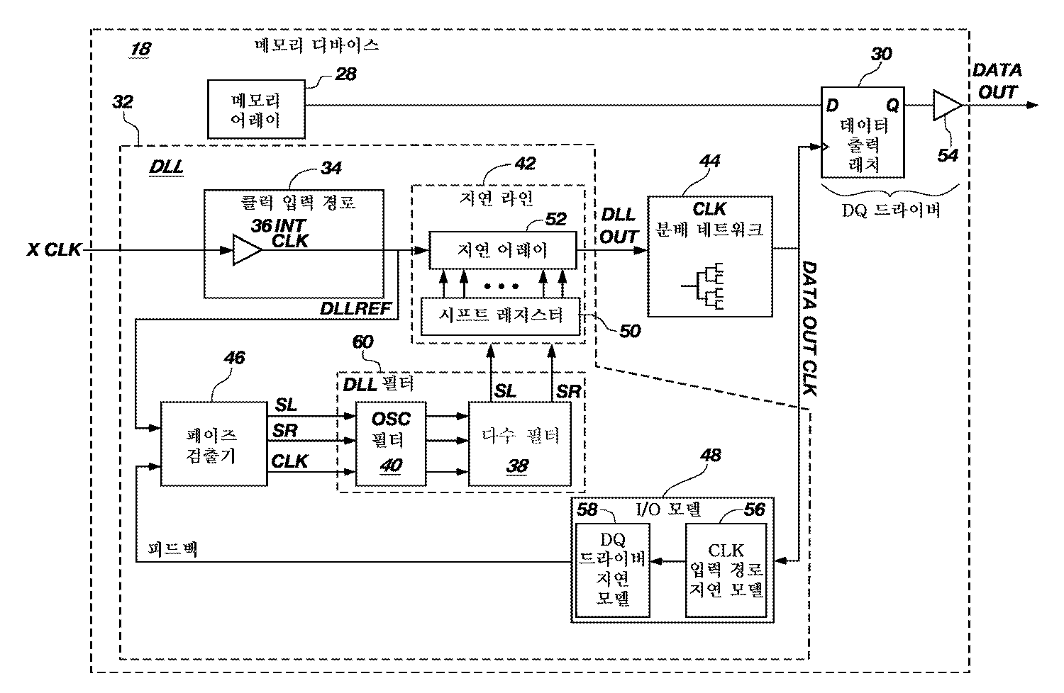
- 지연-고정 루프로서,제1 및 제2 입력들 및 출력을 갖는 지연 라인 - 상기 제1 입력은 클럭 입력 경로를 통해 외부 클럭 신호를 수신하도록 구성되고, 상기 출력은 메모리 디바이스의 출력 드라이버와 연결되도록 구성됨 - ;출력 및 입력을 갖는 I/O 모델 - 상기 I/O 모델의 상기 입력은 상기 메모리 디바이스의 클럭 분배 네트워크를 통해 상기 지연 라인의 출력과 연결되도록 구성되고, 상기 I/O 모델은 상기 출력 드라이버의 지연을 모델링하도록 구성됨 - ;순방향 및 피드백 경로 입력들 및 출력을 갖는 위상 검출기 - 상기 순방향 경로 입력은 상기 지연 라인의 상기 제1 입력에 연결되고, 상기 피드백 경로 입력은 상기 I/O 모델의 출력에 연결됨 - ; 및상기 위상 검출기의 출력에 연결된 입력 및 상기 지연 라인의 상기 제2 입력에 연결된 출력을 갖는 필터 회로 - 상기 필터 회로는 상기 입력에 수신된 입력 신호들로부터의 발진들을 필터링하고 상기 출력에 발진 필터링된 제어 신호들을 생성하기 위해 제1 발진 필터 및 다수 필터를 포함함 -를 포함하는 지연-고정 루프.
- 제7항에 있어서,상기 제1 발진 필터는 발진 필터 입력 신호들 및 발진 필터 출력 신호들을 더 포함하고, 출력 시프트 레프트 명령 상태, 출력 시프트 라이트 명령 상태 및 그 사이의 적어도 하나의 출력 없음 상태를 더 포함하고, 상기 시프트 레프트 명령이 수신되는 경우 상기 출력 시프트 레프트 명령 상태로 천이하고 상기 시프트 라이트 명령이 수신되는 경우 상기 출력 시프트 라이트 명령 상태로 천이하도록 더 구성되는 지연-고정 루프.
- 제8항에 있어서,상기 다수 필터는 다수 필터 입력 신호들 및 다수 필터 출력 신호들을 더 포함하고, 상기 다수 필터 제어 신호들로서 각각의 명령의 최소량의 축적에 대해 출력 시프트 라이트 명령 및 출력 시프트 레프트 명령을 출력하도록 더 구성되는 지연-고정 루프.
- 제9항에 있어서,상기 제1 발진 필터 및 상기 다수 필터는 하나의 출력이 다른 하나의 입력에 함께 직렬로 연결되는 지연-고정 루프.
- 제10항에 있어서,상기 발진 필터 출력 신호들은 상기 다수 필터 입력 신호들에 연결되는 지연-고정 루프.
- 제10항에 있어서,상기 다수 필터 출력 신호들은 상기 발진 필터 입력 신호들에 연결되는 지연-고정 루프.
- 제10항에 있어서,발진 필터 입력 신호들 및 발진 필터 출력 신호들을 포함하는 제2 발진 필터를 더 포함하고, 상기 제1 발진 필터의 상기 발진 필터 출력 신호들은 상기 다수 필터 입력 신호들에 연결되고 상기 다수 필터 출력 신호들은 상기 제2 발진 필터의 상기 발진 필터 입력 신호들에 연결되는 지연-고정 루프.
- 지연-고정 루프로서,외부 클럭 신호와 연결되도록 구성된 입력 및 메모리 디바이스의 출력 드라이버와 연결되도록 구성된 출력을 갖는 순방향 지연 경로 - 상기 순방향 지연 경로는 상기 순방향 지연 경로를 통해 상기 외부 클럭 신호의 지연을 조정하도록 구성된 조정가능한 지연 라인을 포함함 - ;출력 및 입력을 갖는 피드백 지연 경로 - 상기 피드백 지연 경로의 상기 입력은 상기 메모리 디바이스의 상기 출력 드라이버와 연결되도록 구성되고, 상기 피드백 지연 경로는 상기 메모리 디바이스의 상기 출력 드라이버의 지연 모델을 포함함 - ;순방향 및 피드백 경로 입력들 및 출력을 갖는 위상 검출기 - 상기 순방향 경로 입력은 상기 조정가능한 지연 라인에 연결되고 상기 피드백 경로 입력은 상기 피드백 지연 경로의 출력에 연결됨 - ; 및상기 위상 검출기의 상기 출력에 연결된 입력 및 상기 조정가능한 지연 라인에 연결된 출력을 갖는 필터 회로 - 상기 필터 회로는 상기 위상 검출기의 출력으로부터의 발진들을 필터링하고 상기 출력의 상기 조정가능한 지연 라인에 대한 발진 필터링된 제어 신호들을 생성하기 위해 제1 발진 필터 및 다수 필터를 포함함 -를 포함하는 지연-고정 루프.
- 제14항에 있어서,상기 제1 발진 필터 및 상기 다수 필터는 하나의 출력이 다른 하나의 입력과 직렬로 연결되는 지연-고정 루프.
- 제15항에 있어서,상기 발진 필터의 출력은 상기 다수 필터의 입력에 연결되는 지연-고정 루프.
- 제15항에 있어서,상기 다수 필터의 출력은 상기 발진 필터의 입력에 연결되는 지연-고정 루프.
- 제15항에 있어서,제2 발진 필터를 더 포함하고, 상기 제1 발진 필터로부터의 출력 신호들은 상기 다수 필터의 입력 신호들에 연결되고 상기 다수 필터의 출력 신호들은 상기 제2 발진 필터의 입력 신호들에 연결되는 지연-고정 루프.
- 메모리 디바이스로서,그에 연결된 출력 드라이버를 구비한 메모리 어레이; 및상기 출력 드라이버와의 사이에 동작가능하게 연결되고 외부 클럭 신호와 연결되도록 구성된 지연-고정 루프 - 상기 지연-고정 루프는 순방향 및 피드백 지연 경로들을 포함하고, 상기 지연-고정 루프는 상기 순방향 지연 경로의 지연 길이의 변화들을 생성하는 것으로부터 상기 순방향 지연 경로의 발진들을 필터링하도록 구성됨 -를 포함하는 메모리 디바이스.
- 제19항에 있어서,상기 지연-고정 루프는 상기 순방향 지연 경로에서 발진들을 필터링하기 위해 제1 발진 필터 및 다수 필터를 포함하는 메모리 디바이스.
- 제19항에 있어서,상기 제1 발진 필터는 상기 순방향 지연 경로의 발진들을 필터링하도록 구성 되고, 상기 다수 필터는 상기 순방향 지연 경로의 신호들을 평균 필터링하도록 구성되는 메모리 디바이스.
- 제21항에 있어서,상기 제1 발진 필터는 상기 순방향 지연 경로의 발진들을 필터링하고, 다음에 상기 다수 필터는 상기 제1 발진 필터의 출력을 평균 필터링하도록 구성되는 메모리 디바이스.
- 제22항에 있어서,제2 발진 필터는 상기 다수 필터의 출력으로부터 상기 순방향 지연 경로의 발진들을 필터링하는 메모리 디바이스.
- 제21항에 있어서,상기 다수 필터는 상기 순방향 지연 경로에서 평균 필터링하고, 다음에 상기 제1 발진 필터는 상기 다수 필터의 출력으로부터의 발진들을 필터링하는 메모리 디바이스.
- 전자 시스템으로서,프로세서;상기 프로세서에 동작가능하게 연결된 입력 디바이스 및 출력 디바이스 중 적어도 하나; 및상기 프로세서에 동작가능하게 연결된 메모리 디바이스를 포함하고,상기 메모리 디바이스는,그에 연결된 출력 드라이버를 구비한 메모리 어레이; 및상기 출력 드라이버와의 사이에 동작가능하게 연결되고 외부 클럭 신호와 연결되도록 구성된 지연-고정 루프 - 상기 지연-고정 루프는 순방향 및 피드백 지연 경로들을 포함하고, 상기 지연-고정 루프는 상기 순방향 지연 경로의 지연 길이에 대한 변화들을 생성하는 것으로부터 상기 순방향 지연 경로의 발진들을 필터링하도록 구성됨 -를 포함하는 전자 시스템.
- 제25항에 있어서,상기 지연-고정 루프는 상기 순방향 지연 경로의 발진들을 필터링하도록 구성된 적어도 하나의 발진 필터 및 상기 순방향 지연 경로의 신호들을 평균 필터링하도록 구성된 다수 필터를 포함하는 전자 시스템.
- 클럭 동기화 방법으로서,외부 클럭 신호를 순방향 루프 경로로 입력하는 단계;순방향 루프 경로 지연과 피드백 루프 경로 지연 사이의 위상차를 검출하는 단계;상기 순방향 루프 경로 지연을 조정하기 위한 제어 신호들을 생성하기 위해 상기 위상차로부터 발진들을 필터링하는 단계;상기 제어 신호들에 응답하여 상기 순방향 루프 경로 지연을 조정하는 단계; 및상기 순방향 루프 경로의 출력에서 출력 클럭을 생성하는 단계를 포함하는 클럭 동기화 방법.
- 제27항에 있어서,필터링하는 단계는 제1 발진 필터를 이용하여 상기 위상차로부터의 발진들을 필터링하는 단계 및 다수 필터를 이용하여 상기 위상차를 평균 필터링하는 단계를 포함하는 클럭 동기화 방법.
- 제28항에 있어서,상기 제1 발진 필터의 상기 위상차로부터 발진들을 먼저 필터링하고 다음으로 상기 다수 필터에서 상기 제1 발진 필터의 출력을 평균 필터링하는 단계를 더 포함하고, 상기 다수 필터의 출력은 상기 제어 신호들을 포함하는 클럭 동기화 방법.
- 제29항에 있어서,제2 발진 필터에서 상기 다수 필터의 출력을 필터링하는 제2 발진을 더 포함하고, 상기 제2 발진 필터의 출력은 상기 제어 신호들을 포함하는 클럭 동기화 방법.
- 제28항에 있어서,상기 다수 필터의 상기 위상차를 먼저 평균 필터링하고, 다음에 상기 제1 발진 필터에서 상기 다수 필터의 출력을 발진 필터링하고, 상기 제1 발진 필터의 출력은 상기 제어 신호들을 포함하는 클럭 동기화 방법.
- 복수의 집적 회로 메모리 디바이스들을 포함하는 반도체 웨이퍼로서,각각의 메모리 디바이스는,그에 연결된 출력 드라이버를 구비한 메모리 어레이; 및상기 출력 드라이버와의 사이에 동작가능하게 연결되고 외부 클럭 신호와 연결되도록 구성된 지연-고정 루프 - 상기 지연-고정 루프는 순방향 및 피드백 지연 경로들을 포함하고, 상기 지연-고정 루프는 상기 순방향 지연 경로의 지연 길이의 변화들을 생성하는 것으로부터 상기 순방향 지연 경로에서 발진들을 필터링하도록 구성됨 -를 포함하는 반도체 웨이퍼.
Applications Claiming Priority (2)
| Application Number | Priority Date | Filing Date | Title |
|---|---|---|---|
| US11/447,740 | 2006-06-05 | ||
| US11/447,740 US7277357B1 (en) | 2006-06-05 | 2006-06-05 | Method and apparatus for reducing oscillation in synchronous circuits |
Publications (2)
| Publication Number | Publication Date |
|---|---|
| KR20090015136A true KR20090015136A (ko) | 2009-02-11 |
| KR101067590B1 KR101067590B1 (ko) | 2011-09-27 |
Family
ID=38535825
Family Applications (1)
| Application Number | Title | Priority Date | Filing Date |
|---|---|---|---|
| KR1020087031337A KR101067590B1 (ko) | 2006-06-05 | 2007-06-05 | 동기 회로에서 발진을 감소시키기 위한 방법 및 장치 |
Country Status (4)
| Country | Link |
|---|---|
| US (5) | US7277357B1 (ko) |
| KR (1) | KR101067590B1 (ko) |
| CN (1) | CN101485091B (ko) |
| WO (1) | WO2007143650A2 (ko) |
Cited By (1)
| Publication number | Priority date | Publication date | Assignee | Title |
|---|---|---|---|---|
| KR20200141383A (ko) * | 2019-06-10 | 2020-12-18 | 삼성전자주식회사 | 큐 페어 기반 NVMeoF 이니시에이터-타겟 시스템에서 I/O 전송을 위한 방법 및 시스템 |
Families Citing this family (20)
| Publication number | Priority date | Publication date | Assignee | Title |
|---|---|---|---|---|
| US7405996B2 (en) * | 2006-04-21 | 2008-07-29 | Infineon Technologies Ag | System and method to synchronize signals in individual integrated circuit components |
| US7277357B1 (en) | 2006-06-05 | 2007-10-02 | Micron Technology, Inc. | Method and apparatus for reducing oscillation in synchronous circuits |
| WO2008100843A2 (en) * | 2007-02-12 | 2008-08-21 | Rambus Inc. | Correction of voltage offset and clock offset for sampling near zero-crossing point |
| US7804344B2 (en) * | 2007-04-20 | 2010-09-28 | Micron Technology, Inc. | Periodic signal synchronization apparatus, systems, and methods |
| US7701272B2 (en) * | 2007-05-31 | 2010-04-20 | Micron Technology, Inc. | Method and apparatus for output data synchronization with system clock |
| US20080315927A1 (en) * | 2007-06-11 | 2008-12-25 | Hynix Semiconductor Inc. | Frequency adjusting apparatus and dll circuit including the same |
| US7737742B2 (en) * | 2008-02-14 | 2010-06-15 | Qimonda Ag | Delay locked loop |
| JP2010114795A (ja) * | 2008-11-10 | 2010-05-20 | Nec Electronics Corp | 遅延制御方法および遅延装置 |
| US8232823B1 (en) * | 2009-06-05 | 2012-07-31 | Altera Corporation | Frequency control clock tuning circuitry |
| JP2011060364A (ja) * | 2009-09-08 | 2011-03-24 | Elpida Memory Inc | クロック生成回路及びこれを備える半導体装置並びにデータ処理システム |
| KR20110131765A (ko) * | 2010-05-31 | 2011-12-07 | 주식회사 하이닉스반도체 | 위상 보정 회로 및 이를 이용한 데이터 정렬 회로 |
| KR101212724B1 (ko) * | 2010-05-31 | 2012-12-14 | 에스케이하이닉스 주식회사 | 클럭발생회로 및 그를 이용한 지연고정루프 |
| KR20110134197A (ko) * | 2010-06-08 | 2011-12-14 | 삼성전자주식회사 | 전압제어지연라인, 상기 전압제어지연라인을 구비하는 지연고정루프회로 및 다중위상클럭생성기 |
| US8482992B2 (en) * | 2011-07-28 | 2013-07-09 | Elite Semiconductor Memory Technology Inc. | Method of controlling operations of a delay locked loop of a dynamic random access memory |
| JP5811914B2 (ja) * | 2012-03-19 | 2015-11-11 | 富士通株式会社 | 位相同期回路および位相比較方法 |
| JP5940413B2 (ja) * | 2012-08-10 | 2016-06-29 | ルネサスエレクトロニクス株式会社 | 半導体装置及び電子装置 |
| KR102020991B1 (ko) * | 2013-03-15 | 2019-09-11 | 삼성전자주식회사 | 듀얼 지연동기회로를 가지는 동기 반도체 메모리 장치 및 듀얼 지연동기회로의 운영방법 |
| US10580477B2 (en) * | 2018-04-05 | 2020-03-03 | Nanya Technology Corporation | Control circuit and control method for controlling delay lock loop in dynamic random access memory |
| US11916559B2 (en) * | 2021-12-31 | 2024-02-27 | SambaNova Systems, Inc. | Delay-locked loop with widened lock range |
| US11923853B2 (en) | 2022-02-25 | 2024-03-05 | Nvidia Corp. | Circuit structures to measure flip-flop timing characteristics |
Family Cites Families (42)
| Publication number | Priority date | Publication date | Assignee | Title |
|---|---|---|---|---|
| US5544203A (en) * | 1993-02-17 | 1996-08-06 | Texas Instruments Incorporated | Fine resolution digital delay line with coarse and fine adjustment stages |
| US5537068A (en) | 1994-09-06 | 1996-07-16 | Intel Corporation | Differential delay line clock generator |
| US5828250A (en) | 1994-09-06 | 1998-10-27 | Intel Corporation | Differential delay line clock generator with feedback phase control |
| JP2755183B2 (ja) * | 1994-09-26 | 1998-05-20 | 日本電気株式会社 | 低消費電力動作用のクロックジェネレータ/コントローラ内蔵lsi |
| US5818788A (en) * | 1997-05-30 | 1998-10-06 | Nec Corporation | Circuit technique for logic integrated DRAM with SIMD architecture and a method for controlling low-power, high-speed and highly reliable operation |
| KR100269316B1 (ko) | 1997-12-02 | 2000-10-16 | 윤종용 | 동기지연회로가결합된지연동기루프(dll)및위상동기루프(pll) |
| US6069507A (en) | 1998-05-22 | 2000-05-30 | Silicon Magic Corporation | Circuit and method for reducing delay line length in delay-locked loops |
| JP3839959B2 (ja) | 1998-06-05 | 2006-11-01 | パイオニア株式会社 | 情報再生装置、情報記録装置、情報再生方法及び情報記録方法 |
| US6300807B1 (en) | 1998-09-04 | 2001-10-09 | Hitachi, Ltd. | Timing-control circuit device and clock distribution system |
| US6100735A (en) | 1998-11-19 | 2000-08-08 | Centillium Communications, Inc. | Segmented dual delay-locked loop for precise variable-phase clock generation |
| US6446180B2 (en) | 1999-07-19 | 2002-09-03 | Micron Technology, Inc. | Memory device with synchronized output path |
| US6388480B1 (en) * | 1999-08-30 | 2002-05-14 | Micron Technology, Inc. | Method and apparatus for reducing the lock time of DLL |
| US6240042B1 (en) | 1999-09-02 | 2001-05-29 | Micron Technology, Inc. | Output circuit for a double data rate dynamic random access memory, double data rate dynamic random access memory, method of clocking data out from a double data rate dynamic random access memory and method of providing a data strobe signal |
| US6476652B1 (en) | 1999-11-01 | 2002-11-05 | Hynix Semiconductor Inc. | Delay locked loop for use in synchronous dynamic random access memory |
| KR100335499B1 (ko) | 1999-12-30 | 2002-05-08 | 윤종용 | 지연시간차를 보상하는 폐루프 아날로그 동기화 지연 시간반영 기법 구조의 클락 발생회로 |
| US6323705B1 (en) | 2000-04-25 | 2001-11-27 | Winbond Electronics Corporation | Double cycle lock approach in delay lock loop circuit |
| JP2001326563A (ja) * | 2000-05-18 | 2001-11-22 | Mitsubishi Electric Corp | Dll回路 |
| US6535043B2 (en) | 2000-05-26 | 2003-03-18 | Lattice Semiconductor Corp | Clock signal selection system, method of generating a clock signal and programmable clock manager including same |
| KR100543934B1 (ko) | 2000-05-31 | 2006-01-23 | 주식회사 하이닉스반도체 | 반도체 메모리 장치에서 어드레스 및 데이터 억세스타임을 고속으로 하는 제어 및 어드레스 장치 |
| US6445231B1 (en) | 2000-06-01 | 2002-09-03 | Micron Technology, Inc. | Digital dual-loop DLL design using coarse and fine loops |
| KR100416695B1 (ko) * | 2000-06-30 | 2004-02-05 | 주식회사 하이닉스반도체 | 노이즈 제어가 가능한 지연고정루프 |
| US6636093B1 (en) | 2000-07-14 | 2003-10-21 | Micron Technology, Inc. | Compensation for a delay locked loop |
| KR100513806B1 (ko) | 2000-12-30 | 2005-09-13 | 주식회사 하이닉스반도체 | 반도체 장치 |
| JP3575430B2 (ja) | 2001-02-01 | 2004-10-13 | 日本電気株式会社 | 2段階可変長遅延回路 |
| US6522209B2 (en) * | 2001-05-17 | 2003-02-18 | Texas Instruments Incorporated | Oscillator averaging phase shift generator |
| US6950487B2 (en) | 2001-05-18 | 2005-09-27 | Micron Technology, Inc. | Phase splitter using digital delay locked loops |
| US6556643B2 (en) | 2001-08-27 | 2003-04-29 | Micron Technology, Inc. | Majority filter counter circuit |
| JP2003163592A (ja) * | 2001-11-26 | 2003-06-06 | Mitsubishi Electric Corp | 位相比較器およびそれを用いたクロック発生回路 |
| KR100424180B1 (ko) | 2001-12-21 | 2004-03-24 | 주식회사 하이닉스반도체 | 듀티 사이클 보상 기능을 갖는 지연 고정 루프 회로 |
| US6774687B2 (en) | 2002-03-11 | 2004-08-10 | Micron Technology, Inc. | Method and apparatus for characterizing a delay locked loop |
| KR100507877B1 (ko) * | 2002-03-28 | 2005-08-18 | 주식회사 하이닉스반도체 | 면적 축소용 알디엘엘 회로 |
| US6795348B2 (en) * | 2002-05-29 | 2004-09-21 | Micron Technology, Inc. | Method and apparatus for erasing flash memory |
| US6621762B1 (en) * | 2002-05-29 | 2003-09-16 | Micron Technology, Inc. | Non-volatile delay register |
| US6891415B2 (en) | 2002-06-11 | 2005-05-10 | Micron Technology, Inc. | Method and apparatus for enabling a timing synchronization circuit |
| US6728163B2 (en) | 2002-08-23 | 2004-04-27 | Micron Technology, Inc. | Controlling a delay lock loop circuit |
| US6839301B2 (en) * | 2003-04-28 | 2005-01-04 | Micron Technology, Inc. | Method and apparatus for improving stability and lock time for synchronous circuits |
| US7129794B2 (en) | 2003-07-21 | 2006-10-31 | Micron Technology, Inc. | Phase detector for reducing noise |
| US7221202B1 (en) * | 2004-09-15 | 2007-05-22 | Cypress Semiconductor Corporation | Delay-locked loop with reduced susceptibility to false lock |
| KR100594297B1 (ko) * | 2004-10-12 | 2006-06-30 | 삼성전자주식회사 | 외부 클럭 신호의 주파수에 순응하는 발진기를 이용하는지연 동기 루프 및 방법 |
| US20070205817A1 (en) * | 2006-03-03 | 2007-09-06 | Tyler Gomm | Method, circuit and system for detecting a locked state of a clock synchronization circuit |
| US7277357B1 (en) * | 2006-06-05 | 2007-10-02 | Micron Technology, Inc. | Method and apparatus for reducing oscillation in synchronous circuits |
| US8145925B2 (en) * | 2007-12-21 | 2012-03-27 | Mosaid Technologies Incorporated | Non-volatile semiconductor memory device with power saving feature |
-
2006
- 2006-06-05 US US11/447,740 patent/US7277357B1/en active Active
-
2007
- 2007-06-05 KR KR1020087031337A patent/KR101067590B1/ko active IP Right Grant
- 2007-06-05 CN CN2007800255085A patent/CN101485091B/zh active Active
- 2007-06-05 WO PCT/US2007/070407 patent/WO2007143650A2/en active Application Filing
- 2007-08-30 US US11/847,841 patent/US7596052B2/en active Active
-
2009
- 2009-09-29 US US12/569,591 patent/US7965580B2/en active Active
-
2011
- 2011-06-13 US US13/159,094 patent/US8134886B2/en active Active
-
2012
- 2012-03-13 US US13/418,623 patent/US8462579B2/en active Active
Cited By (1)
| Publication number | Priority date | Publication date | Assignee | Title |
|---|---|---|---|---|
| KR20200141383A (ko) * | 2019-06-10 | 2020-12-18 | 삼성전자주식회사 | 큐 페어 기반 NVMeoF 이니시에이터-타겟 시스템에서 I/O 전송을 위한 방법 및 시스템 |
Also Published As
| Publication number | Publication date |
|---|---|
| US8462579B2 (en) | 2013-06-11 |
| WO2007143650A3 (en) | 2008-02-21 |
| US7965580B2 (en) | 2011-06-21 |
| US20080042702A1 (en) | 2008-02-21 |
| US7596052B2 (en) | 2009-09-29 |
| CN101485091A (zh) | 2009-07-15 |
| WO2007143650A2 (en) | 2007-12-13 |
| US20110242915A1 (en) | 2011-10-06 |
| US20120169388A1 (en) | 2012-07-05 |
| KR101067590B1 (ko) | 2011-09-27 |
| US8134886B2 (en) | 2012-03-13 |
| CN101485091B (zh) | 2013-06-05 |
| US7277357B1 (en) | 2007-10-02 |
| US20100014377A1 (en) | 2010-01-21 |
Similar Documents
| Publication | Publication Date | Title |
|---|---|---|
| KR101067590B1 (ko) | 동기 회로에서 발진을 감소시키기 위한 방법 및 장치 | |
| US7622969B2 (en) | Methods, devices, and systems for a delay locked loop having a frequency divided feedback clock | |
| KR100624871B1 (ko) | 2배 데이터 속도 타이밍을 위한 클록 대기 보상 회로 | |
| US9536591B1 (en) | Staggered DLL clocking on N-Detect QED to minimize clock command and delay path | |
| KR100625128B1 (ko) | 버퍼 메모리 시스템에서 신뢰성있는 전송을 제공하기 위한 시스템 및 방법 | |
| KR100866601B1 (ko) | 반도체 장치의 종단 저항을 제어할 수 있는 장치 및 방법 | |
| US8164368B2 (en) | Power savings mode for memory systems | |
| KR100740076B1 (ko) | 회로 기판상의 지연을 조정하는 디지탈 시스템 | |
| US7672191B2 (en) | Data output control circuit | |
| KR20130139348A (ko) | 데이터 블록에 명령을 제공하기 위한 명령 경로, 장치, 및 방법 | |
| JP2006260322A (ja) | メモリインターフェイス制御回路 | |
| US10026462B1 (en) | Apparatuses and methods for providing constant DQS-DQ delay in a memory device | |
| KR100883140B1 (ko) | 데이터 출력 제어회로, 반도체 메모리 장치 및 그의 동작방법 | |
| US8134391B2 (en) | Semiconductor devices with signal synchronization circuits | |
| KR102016532B1 (ko) | 반도체 장치 및 그의 구동방법 | |
| US10698846B2 (en) | DDR SDRAM physical layer interface circuit and DDR SDRAM control device | |
| TWI434515B (zh) | 於外部時脈之頻率改變之後根據相位差來自動重置之延遲鎖定迴路系統以及於外部時脈之頻率改變之後自動重置延遲鎖定迴路的方法 | |
| US20150130521A1 (en) | Method, circuit and system for detecting a locked state of a clock synchronization circuit | |
| US9304531B2 (en) | Dynamically scaling voltage/frequency | |
| KR102058666B1 (ko) | 펄스 신호 생성 회로 및 그의 동작 방법 | |
| JP2004070800A (ja) | メモリシステム及びメモリモジュール | |
| KR20110138141A (ko) | 위상 오차에 대한 루프 대역폭 의존성을 가지는 지연고정루프 | |
| JP2012168754A (ja) | メモリインタフェース回路 | |
| JP2011242838A (ja) | メモリインタフェース回路 | |
| KR20060040966A (ko) | 지연 동기 루프 |
Legal Events
| Date | Code | Title | Description |
|---|---|---|---|
| A201 | Request for examination | ||
| E902 | Notification of reason for refusal | ||
| E701 | Decision to grant or registration of patent right | ||
| GRNT | Written decision to grant | ||
| FPAY | Annual fee payment |
Payment date: 20140901 Year of fee payment: 4 |
|
| FPAY | Annual fee payment |
Payment date: 20150819 Year of fee payment: 5 |
|
| FPAY | Annual fee payment |
Payment date: 20160818 Year of fee payment: 6 |
|
| FPAY | Annual fee payment |
Payment date: 20170822 Year of fee payment: 7 |
|
| FPAY | Annual fee payment |
Payment date: 20180903 Year of fee payment: 8 |
|
| FPAY | Annual fee payment |
Payment date: 20190909 Year of fee payment: 9 |