KR101027840B1 - Copper alloy plate material for electrical/electronic equipment and process for producing the same - Google Patents
Copper alloy plate material for electrical/electronic equipment and process for producing the same Download PDFInfo
- Publication number
- KR101027840B1 KR101027840B1 KR1020097004769A KR20097004769A KR101027840B1 KR 101027840 B1 KR101027840 B1 KR 101027840B1 KR 1020097004769 A KR1020097004769 A KR 1020097004769A KR 20097004769 A KR20097004769 A KR 20097004769A KR 101027840 B1 KR101027840 B1 KR 101027840B1
- Authority
- KR
- South Korea
- Prior art keywords
- copper alloy
- compound
- alloy sheet
- mass
- intermetallic compound
- Prior art date
Links
Images

Classifications
-
- C—CHEMISTRY; METALLURGY
- C22—METALLURGY; FERROUS OR NON-FERROUS ALLOYS; TREATMENT OF ALLOYS OR NON-FERROUS METALS
- C22C—ALLOYS
- C22C9/00—Alloys based on copper
- C22C9/06—Alloys based on copper with nickel or cobalt as the next major constituent
-
- C—CHEMISTRY; METALLURGY
- C22—METALLURGY; FERROUS OR NON-FERROUS ALLOYS; TREATMENT OF ALLOYS OR NON-FERROUS METALS
- C22C—ALLOYS
- C22C9/00—Alloys based on copper
- C22C9/10—Alloys based on copper with silicon as the next major constituent
-
- C—CHEMISTRY; METALLURGY
- C22—METALLURGY; FERROUS OR NON-FERROUS ALLOYS; TREATMENT OF ALLOYS OR NON-FERROUS METALS
- C22F—CHANGING THE PHYSICAL STRUCTURE OF NON-FERROUS METALS AND NON-FERROUS ALLOYS
- C22F1/00—Changing the physical structure of non-ferrous metals or alloys by heat treatment or by hot or cold working
- C22F1/08—Changing the physical structure of non-ferrous metals or alloys by heat treatment or by hot or cold working of copper or alloys based thereon
Landscapes
- Chemical & Material Sciences (AREA)
- Engineering & Computer Science (AREA)
- Materials Engineering (AREA)
- Mechanical Engineering (AREA)
- Metallurgy (AREA)
- Organic Chemistry (AREA)
- Physics & Mathematics (AREA)
- Thermal Sciences (AREA)
- Crystallography & Structural Chemistry (AREA)
- Conductive Materials (AREA)
Abstract
Ni를 2.0∼5.0mass%, Si를 0.43∼1.5mass% 함유하고, 잔부가 Cu와 불가피한 불순물로 이루어진 동합금으로 형성되는 동합금 판재로서, Ni와 Si를 합계로 50mass%이상 포함한 3종류의 금속간화합물 A, B, C를 함유하고, 상기 금속간화합물 A의 화합물지름은 0.3㎛ 이상 2㎛ 이하이고, 상기 금속간화합물 B의 화합물지름은 0.05㎛ 이상 0.3㎛ 미만이며, 상기 금속간화합물 C의 화합물지름은 0.001㎛를 넘고 0.05㎛ 미만인 전기ㆍ전자기기용 동합금 판재.A copper alloy sheet containing 2.0 to 5.0 mass% of Ni and 0.43 to 1.5 mass% of Si and the balance being formed of a copper alloy composed of Cu and unavoidable impurities. Three kinds of intermetallic compounds containing 50 mass% or more of Ni and Si in total A, B, and C, wherein the compound diameter of the intermetallic compound A is 0.3 µm or more and 2 µm or less, and the compound diameter of the intermetallic compound B is 0.05 µm or more and less than 0.3 µm, and the compound of the intermetallic compound C Copper alloy sheet for electric and electronic devices with a diameter of more than 0.001 µm and less than 0.05 µm.
Description
본 발명은, 전기ㆍ전자기기에 적합한 Cu-Ni-Si계 동합금 판재에 관한 것이다.The present invention relates to a Cu-Ni-Si-based copper alloy sheet material suitable for electric and electronic equipment.
종래, 전기ㆍ전자기기용 재료로는, 철계 재료 외에, 전기 및 열전도성이 뛰어난 인청동, 단동, 황동, 코르슨 합금 등의 동계 재료가 널리 이용되고 있다. 근래, 전기ㆍ전자기기에는 소형화, 경량화, 고밀도 실장화 등의 요구가 높아지고, 이에 적용되는 동계 재료에는, 강도, 도전성, 내응력완화특성, 구부림가공성, 도금성, 프레스성, 내열성 등의 향상이 요구되고 있다.Background Art Conventionally, as materials for electric and electronic devices, copper-based materials such as phosphor bronze, single copper, brass, and Corson alloy having excellent electrical and thermal conductivity are widely used in addition to iron-based materials. In recent years, demands for miniaturization, weight reduction, high density mounting, etc. have increased in electric and electronic devices, and in the same type of copper materials, the improvement in strength, conductivity, stress relaxation resistance, bending workability, plating property, press resistance, heat resistance, etc. It is required.
그 중에서, Cu중에 Ni와 Si를 첨가하여 그 Ni-Si계 화합물의 석출물을 형성시킨 코르슨 합금은, 많은 석출형 합금 중에서는 강화 능력이 매우 높은 Cu-Ni-Si계 합금으로, 예를 들면, CDA(Copper Development Association)에 등록된 CDA702 50 합금이 시판되고 있다.Among them, the Corson alloy in which Ni and Si are added to Cu to form precipitates of the Ni-Si-based compound is a Cu-Ni-Si-based alloy having a very high reinforcing ability among many precipitated alloys. , A CDA702 50 alloy registered with the Copper Development Association (CDA) is commercially available.
또한, Cu-Ni-Si계 합금으로 Ni-Si계 화합물의 분포 상태를 규정하여 특성을 개선한 합금이 제안되어 있다(예를 들면, 일본특허공개공보2005-298920호, 일본특허공개공보2001-49369호).In addition, alloys having improved properties by defining distribution states of Ni-Si-based compounds as Cu-Ni-Si-based alloys have been proposed (for example, Japanese Patent Laid-Open No. 2005-298920 and Japanese Patent Laid-Open No. 2001-). 49369).
그러나, 상기 CDA70250 합금이나 일본특허공개공보2005-298920호와 일본특허공개공보2001-49369호에 기재된 코르손 합금에 의해서는, 전기ㆍ전자기기용 재료에 요구되는 특성, 특히 도금성, 프레스성, 내열성에 있어서 충분한 특성을 얻을 수 없었다.However, with the CDA70250 alloy and the Corson alloys described in Japanese Patent Laid-Open No. 2005-298920 and Japanese Patent Laid-Open No. 2001-49369, the characteristics required for materials for electric and electronic devices, in particular plating properties, press resistance, and heat resistance Sufficient characteristics could not be obtained.
이러한 상황에 비추어, 본 발명은, 특히, 도금성, 프레스성, 내열성이 뛰어난 전기ㆍ전자기기용의 리드 프레임, 코넥터, 단자, 릴레이, 스위치 등에 적합한 동합금 판재 및 그 제조방법을 제공하는 것을 과제로 한다.In view of such a situation, an object of the present invention is to provide a copper alloy sheet material suitable for a lead frame, a connector, a terminal, a relay, a switch, and the like for an electric / electronic device, which is particularly excellent in plating property, press resistance, and heat resistance, and a manufacturing method thereof. .
본 발명자들은, 전기ㆍ전자기기용에 적합한 동합금 판재에 대하여 연구를 행하여, 동합금 판재 중에 분산하는 화합물의 입자지름(화합물 입자의 직경) 및 그 분산밀도와, 도금성, 프레스성, 내열성 등의 특성과의 관계에 대하여 검토하고, 상기 입자지름 및 분산밀도를 적정하게 규정하는 것에 의해 상기 특성을 개선할 수 있는 것을 지견하고, 이 지견에 기초하여 검토를 더 진행하여 본 발명을 완성시키기에 이르렀다.MEANS TO SOLVE THE PROBLEM The present inventors researched the copper alloy board material suitable for electrical and electronic equipment, and the particle diameter (diameter diameter of a compound particle) of the compound disperse | distributed in a copper alloy board material, its dispersion density, and characteristics, such as plating property, press resistance, and heat resistance, Examining the relationship, the inventors found that the above characteristics could be improved by appropriately defining the particle diameter and the dispersion density. Based on this finding, further studies were made to complete the present invention.
본 발명에 의하면, 이하의 수단이 제공된다:According to the present invention, the following means are provided:
(1) Ni를 2.0∼5.0mass%, Si를 0.43∼1.5mass% 함유하고, 잔부가 Cu와 불가피한 불순물로 이루어진 동합금으로 형성되는 동합금 판재로서, Ni와 Si를 합계로 50mass% 이상 포함한 3종류의 금속간화합물 A, B, C를 함유하고, 상기 금속간화합물 A의 화합물지름(그 화합물의 지름의 최소치와 최대치의 산술 평균이다. 이하, 동일)은 0.3㎛이상 2㎛이하이고, 상기 금속간화합물 B의 화합물지름은 0.05㎛이상 0.3㎛미만이며, 상기 금속간화합물 C의 화합물지름은 0.001㎛를 넘고 0.05㎛미만 인 것을 특징으로 하는 전기ㆍ전자기기용 동합금 판재, (1) A copper alloy sheet containing 2.0 to 5.0 mass% of Ni and 0.43 to 1.5 mass% of Si, with the balance being formed of a copper alloy composed of Cu and unavoidable impurities. The intermetallic compound A, B, and C are contained, and the compound diameter of the intermetallic compound A (the arithmetic mean of the minimum and maximum diameters of the compound. Hereinafter, the same) is 0.3 µm or more and 2 µm or less. The compound diameter of Compound B is 0.05 µm or more and less than 0.3 µm, and the compound diameter of the intermetallic compound C is more than 0.001 µm and less than 0.05 µm,
(2) 상기 금속간화합물 A의 분산 밀도 a, 상기 금속간화합물 B의 분산 밀도 b 및 상기 금속간화합물 C의 분산 밀도 c가, 관계식[a/(b+c)≤0.010]를 만족하는 것을 특징으로 하는 (1)항에 기재된 전기ㆍ전자기기용 동합금 판재, (2) The dispersion density a of the intermetallic compound A, the dispersion density b of the intermetallic compound B, and the dispersion density c of the intermetallic compound C satisfy the relation [a / (b + c) ≦ 0.010]. Copper alloy sheet material for electric and electronic equipment described in item (1),
(3) 상기 금속간화합물 B의 분산 밀도 b 및 상기 금속간화합물 C의 분산 밀도 c가, 관계식[0.001≤(b/c)≤0.10]를 만족하는 것을 특징으로 하는 (1) 또는 (2)항에 기재된 전기ㆍ전자기기용 동합금 판재, (3) (1) or (2), wherein the dispersion density b of the intermetallic compound B and the dispersion density c of the intermetallic compound C satisfy a relational expression [0.001 ≦ (b / c) ≦ 0.10]. Copper alloy sheet material for electrical and electronic equipment
(4) 상기 동합금 판재의 압연 방향에 수직인 단면에 있어서의 결정입자지름의 가로 길이 x(㎛)와 세로 길이 y(㎛)가, 관계식[x/y≥2]를 만족하는 것을 특징으로 하는 (1) 내지 (3) 중의 어느 한 항에 기재된 전기ㆍ전자기기용 동합금 판재, (4) The transverse length x (μm) and the longitudinal length y (μm) of the crystal grain diameter in the cross section perpendicular to the rolling direction of the copper alloy sheet material satisfy the relational expression [x / y ≧ 2]. Copper alloy sheet material for electric and electronic equipment in any one of (1)-(3),
(5) 상기 동합금 판재가, B, Al, As, Hf, Zr, Cr, Ti, C, Co, Fe, P, In, Sb, Mn, Ta, V, Sn, Zn 및 Mg로 이루어진 군으로부터 선택되는 적어도 1개를 합계로 0.005∼1.5mass% 더 함유하는 것을 특징으로 하는 (1) 내지 (4) 중의 어느 한 항에 기재된 전기ㆍ전자기기용 동합금 판재,(5) The copper alloy sheet material is selected from the group consisting of B, Al, As, Hf, Zr, Cr, Ti, C, Co, Fe, P, In, Sb, Mn, Ta, V, Sn, Zn and Mg Copper alloy sheet material for electrical and electronic equipment according to any one of items (1) to (4), further comprising 0.005 to 1.5 mass% of at least one of
(6) Ni를 2.0∼5.0mass%, Si를 0.43∼1.5mass% 함유하고, 잔부가 Cu와 불가피한 불순물로 이루어진 동합금 주괴를 850∼950℃에서 2∼10시간 재열하는 스텝과, 상기 재열된 동합금 주괴를 100∼500초간 열간 압연하여 동합금 판재로 하는 스텝과, 상기 열간압연된 동합금 판재를 600∼800℃가 될 때까지 급랭하는 스텝과, 상기 급랭된 동합금 판재를 400∼550℃에서 1∼4시간 시효 열처리를 하는 스텝을 가진 것을 특징으로 하는 전기ㆍ전자기기용 동합금 판재의 제조 방법, 및 (6) a step of reheating a copper alloy ingot containing 2.0 to 5.0 mass% of Ni and 0.43 to 1.5 mass% of Si, the balance of Cu and an unavoidable impurity at 850 to 950 ° C for 2 to 10 hours, and the reheated copper alloy Hot rolling the ingot for 100 to 500 seconds to form a copper alloy sheet, quenching the hot rolled copper alloy sheet to 600 to 800 ° C., and the quenched copper alloy sheet to 1 to 4 at 400 to 550 ° C. A method for producing a copper alloy sheet for electric and electronic equipment, comprising the step of performing time aging heat treatment, and
(7) 상기 동합금 주괴가, B, Al, As, Hf, Zr, Cr, Ti, C, Co, Fe, P, In, Sb, Mn, Ta, V, Sn, Zn 및 Mg로 이루어진 군으로부터 선택되는 적어도 1개를 합계하여 0.005∼1.5mass% 더 함유하는 것을 특징으로 하는 (6)항에 기재된 전기ㆍ전자기기용 동합금 판재의 제조 방법.(7) The copper alloy ingot is selected from the group consisting of B, Al, As, Hf, Zr, Cr, Ti, C, Co, Fe, P, In, Sb, Mn, Ta, V, Sn, Zn and Mg The manufacturing method of the copper alloy plate material for electrical and electronic equipment of the said (6) description which contains 0.005-1.5 mass% of at least 1 more in total.
본 발명의 상기 및 다른 특징 및 이점은, 적절히 첨부한 도면을 참조하여, 하기의 기재로부터 보다 명백해질 것이다.The above, the other characteristics, and the advantage of this invention will become clear from the following description with reference to attached drawing suitably.
[발명을 실시하기 위한 최선의 형태]BEST MODE FOR CARRYING OUT THE INVENTION [
본 발명의 전기ㆍ전자기기용에 적합한 동합금 판재의 바람직한 실시형태에 대하여 상세하게 설명한다. 먼저, 본 발명의 동합금 판재에 있어서의 동합금 조성에 대하여 각 합금 원소의 작용 효과와 그 함유량에 대하여 설명한다.EMBODIMENT OF THE INVENTION Preferred embodiment of the copper alloy plate material suitable for the electrical and electronic equipment of this invention is described in detail. First, the effect of each alloying element and its content are demonstrated about the copper alloy composition in the copper alloy plate material of this invention.
Ni와 Si는 Ni-Si화합물을 석출하여 강도향상에 기여한다.Ni and Si precipitate Ni-Si compounds and contribute to the improvement of strength.
Ni의 함유량은 2.0∼5.0mass%, 바람직한 함유량은 2.5∼3.5mass%이다. Si의 함유량은 0.43∼1.5mass%, 바람직한 함유량은 0.5∼0.7mass%, 보다 바람직하게는 0.8∼1.1mass%이다.The content of Ni is 2.0 to 5.0 mass%, and the preferred content is 2.5 to 3.5 mass%. Si content is 0.43-1.5 mass%, preferable content is 0.5-0.7 mass%, More preferably, it is 0.8-1.1 mass%.
이러한 양을 규정한 이유는, 어느 하나가 하한치를 밑돌아도 충분한 강도를 얻을 수 없고, 어느 하나가 상한치를 웃돌아도 강도가 포화하므로, 도전율이 저하하기 때문이다. The reason for specifying such amounts is that the conductivity is lowered even if either of the values falls below the lower limit, and the strength is saturated even if either of them exceeds the upper limit.
Ni와 Si의 질량비는, 특별히 제한하는 것은 아니지만 Ni 1에 대해, Si는 0.2∼0.3의 범위인 것이 바람직하다. 또한 Si의 함유량의 상한은, Si의 함유량이 Ni의 함유량의 약 1/4일 때에 가장 고강도가 되는 것, Si의 함유량이 1.5mass%를 넘으면 열간압연 균열이 발생하기 쉬워지는 것을 근거로 하여 규정하였다.The mass ratio of Ni and Si is not particularly limited, but Si is preferably in the range of 0.2 to 0.3 with respect to Ni 1. The upper limit of the Si content is defined based on the fact that the highest strength is achieved when the Si content is about 1/4 of the Ni content, and that hot rolled cracks are more likely to occur when the Si content exceeds 1.5 mass%. It was.
본 발명의 동합금 판재는, 상기 Ni, Si 외에, B, Al, As, Hf, Zr, Cr, Ti, C, Co, Fe, P, In, Sb, Mn, Ta, V, Sn, Zn 및, Mg로 이루어진 군으로부터 선택되는 적어도 1개를 적량 더 함유시킴으로써 강도 향상이 도모된다. 이들 원소의 함유량은 합계로 0.005∼1.5mass%, 바람직하게는 0.01∼1.0mass%이다. 그 양이 0.005mass% 미만이면 그 효과를 충분히 얻을 수 없고, 1.5mass%를 넘으면 도전율이 저하한다.The copper alloy sheet material of the present invention is, in addition to Ni and Si, B, Al, As, Hf, Zr, Cr, Ti, C, Co, Fe, P, In, Sb, Mn, Ta, V, Sn, Zn, The strength improvement is aimed at by containing an appropriate amount of at least 1 selected from the group which consists of Mg further. Content of these elements is 0.005-1.5 mass% in total, Preferably it is 0.01-1.0 mass%. If the amount is less than 0.005 mass%, the effect cannot be sufficiently obtained. If the amount is more than 1.5 mass%, the conductivity decreases.
본 발명에 있어서, 동(銅) 모상 중에 미세한 Ni-Si계 금속간화합물이 생성하고, 그에 따라 합금의 강도가 증가함과 함께, 전기전도성도 양호해지지만, 본 발명에서는 이 화합물의 크기에 주목하여, 그 화합물의 지름의 최소치와 최대치의 산술 평균을 화합물지름으로 하고, 이 화합물지름에 기초하여 화합물 A, B, 및 C로 분류한다. 그리고, 본 발명에서는 동합금 판재 중에 화합물 B 및 C가 포함되어 있는 것이 필수이다.In the present invention, a fine Ni-Si-based intermetallic compound is produced in the copper matrix phase, thereby increasing the strength of the alloy and improving electrical conductivity, but the present invention pays attention to the size of the compound. The arithmetic mean of the minimum and maximum diameters of the compound is defined as the compound diameter, and classified into compounds A, B, and C based on the compound diameter. In the present invention, it is essential that the compounds B and C are contained in the copper alloy sheet.
화합물의 직경(화합물지름)은 합금 시료로부터 직경 3㎜의 원판을 구멍을 뚫어, 트윈 제트 연마법에 의해 박막에 연마하고, 가속 전압 300㎸의 투과형 전자현미경으로 50000배와 100000배의 사진을 임의의 3개소에서 촬영하고, 그 사진상에서 화합물의 직경과 개수를 측정한다. 이에 따라 그 화합물지름(그 화합물의 지름의 최소치와 최대치의 산술 평균)에 따라 화합물 A, B 및 C로 하였다.The diameter (compound diameter) of the compound is obtained by drilling a disc of diameter 3 mm from the alloy sample and polishing the thin film by twin jet polishing method, and randomly selecting 50000 times and 100000 times images by a transmission electron microscope with an acceleration voltage of 300 kV. Photograph is taken at three places and the diameter and number of the compound are measured on the photograph. Accordingly, compounds A, B, and C were determined according to the compound diameter (the arithmetic mean of the minimum and maximum diameters of the compound).
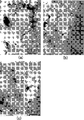
도 1은, 본 발명의 실시예 2의 No.9를 가속 전압 300㎸의 투과형 전자현미경으로 관찰한 예이며, (a), (b)는 5만배, (c)는 10만배의 현미경 사진이다.Fig. 1 is an example of observation of No. 9 of Example 2 of the present invention with a transmission electron microscope with an acceleration voltage of 300 Hz, and (a) and (b) are 50,000 times, and (c) is a 100,000 times microscope photograph. .
화합물 A, B, C의 분산 밀도는, 이하와 같이 구하였다.The dispersion density of the compounds A, B, and C was calculated | required as follows.
(1) 먼저, 임의의 3개소에서 촬영한 사진 중에서 보여진 화합물을 사이즈별로 분류하였다. 여기서, 화합물지름은 그 화합물의 지름의 최소치와 최대치의 산술 평균으로 하였다. (1) First, compounds shown in photographs taken at any three places were classified by size. Here, compound diameter was made into the arithmetic mean of the minimum value and the maximum value of the diameter of the compound.
(2) 그 다음에, 각 사이즈의 화합물의 개수를 세어, 각 사진의 면적에서 제하고, 계속해서 단위면적(㎟)으로 환산하였다. (2) Then, the number of compounds of each size was counted, subtracted from the area of each photograph, and subsequently converted to unit area (mm 2).
(3) 그것을, 5만배, 10만배의 사진의 각각 3매에서 행하여, 합계 6매의 평균치를 구하였다.(3) It carried out from three sheets of 50,000 times and 100,000 times each photograph, and calculated | required the average value of six sheets in total.
Ni와 Si를 합계하여 50mass%이상 포함한 화합물지름이 0.3㎛이상 2㎛이하인 화합물 A는, 화합물 B나 화합물 C와 비교하여 동합금 판재의 인장 강도 등의 특성 향상에의 기여가 작다. 화합물 A는 동합금 판재에 과잉으로 포함되는 것에 의해 오히려 도금성 등을 열화시킨다. 또한 화합물 A가 많으면 특성 향상에 기여하는 화합물 B 및 화합물 C가 줄어드는 경향이 있기 때문에, 화합물 A는 적을수록 좋다. 화합물 A의 분산 밀도 a는, 10개/㎟ 이하가 바람직하다.Compound A having a compound diameter of 0.3 µm or more and 2 µm or less in total containing 50 mass% or more of Ni and Si has a smaller contribution to improving the properties such as tensile strength of the copper alloy sheet as compared with Compound B or Compound C. Compound A deteriorates plating property etc. by being contained excessively in a copper alloy plate material. In addition, since there exists a tendency for the compound B and the compound C which contribute to a characteristic improvement, when there are many compounds A, there is a little compound A so that it is good. As for the dispersion density a of the compound A, 10 piece / mm <2> or less is preferable.
본 발명에 있어서, 화합물 A는, 용해 주조시나 그 응고 과정, 열간 가공시의 비평형적인 열처리시에 생성되는 것이며, 열간 압연 전의 재열처리 혹은 열간 압연 종료후의 용체화(균질화) 처리를 고온에서 실시하거나, 장시간 실시하는 것에 의해 용이하게 소실 혹은 소경화시킬 수 있다. 상기 재열처리는, 공업적으로는 900℃이상, 0.5시간 이상의 조건에서 실시되고 있지만, 이 조건에서는 화합물 A가 잔존하는 경우가 있고, 또한 화합물 A는 열간압연 중에 형성되기도 한다.In the present invention, Compound A is produced at the time of melt casting, at the solidification process, or at the non-equilibrium heat treatment during the hot working, and performs the reheating treatment before hot rolling or the solution (homogenization) treatment after the end of hot rolling at a high temperature. Or it can be easily lost or hardened by carrying out for a long time. Although the said reheating process is industrially performed on 900 degreeC or more and 0.5 hours or more conditions, compound A may remain | survive on this condition, and compound A may be formed during hot rolling.
본 발명에 있어서, Ni와 Si를 합계하여 50mass%이상 포함한 화합물지름이 0.05㎛이상 0.3㎛미만인 화합물 B는 프레스성을 향상시킨다. 즉, 동합금 판재의 동(銅) 모상이 프레스 가공시에 펀치와 다이로 끼워져 변형할 때, 화합물은 경도가 높기 때문에 변형하지 않고 화합물 주변의 동(銅) 모상에 미세한 크랙이 발생하여, 이 크랙이 전파하는 것에 의해 전단가공이 용이해져 프레스성이 향상한다. 이 효과는 화합물의 직경이 0.05㎛미만이라도 0.3㎛이상이라도 충분히는 얻을 수 없다. 화합물 B의 양을 많게 해도 그 효과가 포화하고, 또한 다른 특성에 기여하는 화합물 C의 양이 줄어들어 버린다.In the present invention, Compound B having a compound diameter of 50 mass% or more in total of Ni and Si is 0.05 µm or more and less than 0.3 µm to improve pressability. That is, when the copper base of the copper alloy sheet is deformed by being punched and died during press working, the compound is not hardly deformed due to its high hardness, so that minute cracks are generated on the copper base around the compound. This propagation facilitates shearing and improves pressability. This effect cannot be sufficiently obtained even if the diameter of the compound is less than 0.05 µm and 0.3 µm or more. Even if the amount of the compound B is increased, the effect is saturated, and the amount of the compound C that contributes to other properties decreases.
화합물 B의 입자지름과 분산밀도는 열간 압연에서의 압연 패스 횟수, 압연 패스의 간격 시간, 열간 압연 종료 온도, 압연 종료 후에 물로 담금질할 때까지의 시간 등을 바꾸는 것에 의해 제어할 수 있다. 화합물 B의 분산 밀도 b는, 102∼106개/㎟가 바람직하다.The particle diameter and the dispersion density of the compound B can be controlled by changing the number of rolling passes in hot rolling, the interval time of rolling passes, the hot rolling end temperature, the time until the quenching with water after the end of rolling, and the like. As for the dispersion density b of the compound B, 10 <2> -10 <6> piece / mm <2> is preferable.
본 발명에 있어서, Ni와 Si를 합계하여 50mass%이상 포함한 화합물지름이 0.001㎛를 넘고 0.05㎛미만인 화합물 C는 내열성 향상에 기여한다. 프레스 가공후의 리드 프레임은, 프레스시에 발생한 잔류 응력을 제거하기 위해서 응력제거소둔이 행해지지만, 내열성이 높은 재료는 상기 응력제거소둔에서의 경도의 변화가 작기 때문에 바람직하다. 그러나 화합물 C가 많으면 도전율이 저하한다.In the present invention, compound C having a compound diameter of 50 mass% or more in total of Ni and Si of more than 0.001 µm and less than 0.05 µm contributes to improvement of heat resistance. Although the lead frame after press work is subjected to stress removal annealing in order to remove residual stress generated at the time of pressing, a material having high heat resistance is preferable because the change in hardness in the stress removal annealing is small. However, when there are many compounds C, electrical conductivity will fall.
화합물 C의 화합물지름과 분산 밀도는, 시효 열처리 조건(온도와 시간)을 바꾸는 것에 의해 제어한다. 시효 열처리는 온도가 높고, 시간이 길수록 화합물의 입자지름은 커지고, 도전율은 높아지지만, 반대로 인장 강도는 낮아진다. 한편, 온도가 낮고, 화합물의 입자지름이 작은 경우는 인장강도가 높아져 도전율이 낮아진다. 화합물 C의 분산 밀도 c는, 104∼109개/㎟가 바람직하고, 105∼107개/㎟가 더 바람직하다.The compound diameter and the dispersion density of the compound C are controlled by changing the aging heat treatment conditions (temperature and time). In the aging heat treatment, the temperature is high, and the longer the time, the larger the particle diameter of the compound and the higher the conductivity, but the lower the tensile strength. On the other hand, when the temperature is low and the particle diameter of the compound is small, the tensile strength is increased and the conductivity is low. Dispersion density of the compound C is c, and the 10 4-10 9 / ㎟ preferably, 10 5-10 7 / ㎟ is more preferable.
본 발명에 있어서, 화합물 A의 분산밀도 a와 화합물 B의 분산 밀도 b와 화합물 C의 분산밀도 c가, [a/(b+c)≤0.010]의 관계식을 만족할 때, 프레스성과 강도가 향상하는 것이 명백해진다. a/(b+c)가 0.010을 넘으면 프레스성과 강도가 저하하므로, 도금성도 저하한다.In the present invention, when the dispersion density a of the compound A, the dispersion density b of the compound B, and the dispersion density c of the compound C satisfy the relational expression of [a / (b + c) ≦ 0.010], the pressability and the strength are improved. It becomes clear. When a / (b + c) exceeds 0.010, since pressability and strength fall, plating property also falls.
또한, 본 발명에 있어서, 화합물 B의 분산 밀도 b와 화합물 C의 분산 밀도 c가, [0.001≤(b/c)≤0.10]의 관계식을 만족할 때, 프레스성이 향상하는 것도 알 수 있다. 0.001 미만이면 충분한 프레스성을 얻을 수 없고, 0.10을 넘으면 석출 강화가 부족하여 충분한 강도를 얻을 수 없다.Moreover, in this invention, when the dispersion density b of compound B and the dispersion density c of compound C satisfy | fill the relational formula of [0.001 <(b / c) <0.10], it turns out that pressability improves. If it is less than 0.001, sufficient pressability cannot be obtained, and if it exceeds 0.10, precipitation strengthening will be insufficient and sufficient strength cannot be obtained.
본 발명에 있어서, 화합물 A, B 및 C는, Ni와 Si가 합계하여 50mass%이상 포함되어 있으면 본 발명의 효과를 얻을 수 있다. Ni와 Si는 합계 75mass%이상 포함되어 있는 것이 바람직하다. Ni와 Si 외에 Cu나 다른 원소가 포함되어 있어도 좋다.In the present invention, compounds A, B, and C can obtain the effect of the present invention if Ni and Si are included in total of 50 mass% or more. It is preferable that Ni and Si contain 75 mass% or more in total. Cu and other elements may be included in addition to Ni and Si.
본 발명에 있어서, 화합물 A, B 및 C의 성분 조성은 상기 투과 전자현미경(TEM)에 부속된 EDS(에너지 분산형 분석기)에 의해 적정하게 분석할 수 있다. 그 때, 동(銅) 모상의 영향을 받기 때문에, 얻어진 차트로 동피크치와 백그라운드를 제하고, Ni와 Si와 기타 검출된 원소의 피크치를 가산한 수치로 규격화하여, 화합물에 포함되는 Ni 및 Si의 함유%를 구하였다.In the present invention, the component compositions of the compounds A, B and C can be appropriately analyzed by an EDS (Energy Dispersion Analyzer) attached to the transmission electron microscope (TEM). At that time, since it is influenced by the copper matrix, Ni and Si contained in the compound are normalized to a numerical value obtained by subtracting the copper peak value and the background from the chart obtained, adding the peak values of Ni and Si and other detected elements. % Of was determined.
상기 관계식을 만족하는 화합물 A, B 및 C의 분산 밀도를 가진 동합금 판재는, 예를 들면 하기의 형태로 제조할 수 있다.The copper alloy plate material which has the dispersion density of the compounds A, B, and C which satisfy | fills the said relational formula can be manufactured, for example in the following form.
Ni를 2.0∼5.0mass%, Si를 0.43∼1.5mass%를 함유하는 동합금 주괴를 850∼950℃에서 2∼10시간 재열하고, 이어서 열간압연을 100∼500초간 실시하고, 열간압연 종료 온도를 600∼800℃로서 급랭함으로써 얻을 수 있다. 상기 급랭 조건은 300℃ 이상의 온도 범위에서 냉각 속도를 5∼100℃/초로 하는 것이 바람직하다. 그 후, 냉간압연과 소둔을 필요에 따라서 반복하고, 그 다음에 시효 열처리를 400∼550℃에서 1∼4시간의 조건으로 실시한다. 이에 따라 도금성, 프레스성, 내열성이 뛰어난 동합금 판재를 얻을 수 있다.A copper alloy ingot containing 2.0 to 5.0 mass% of Ni and 0.43 to 1.5 mass% of Si was reheated at 850 to 950 ° C for 2 to 10 hours, followed by hot rolling for 100 to 500 seconds, and the hot rolling finish temperature was 600. It can obtain by rapidly cooling as -800 degreeC. It is preferable that the said quench conditions make cooling rate 5-100 degreeC / sec in 300 degreeC or more temperature range. Thereafter, cold rolling and annealing are repeated as necessary, and then an aging heat treatment is performed at 400 to 550 캜 for 1 to 4 hours. Thereby, the copper alloy plate material excellent in plating property, press property, and heat resistance can be obtained.
보다 바람직한 조건으로서는, 재열조건은 875∼925℃×4∼6시간, 열간 압연 시간은 400∼600초, 열간 압연 종료 온도는 650∼750℃, 급랭 조건은 20∼50℃/초 (300℃ 이상의 온도 범위), 시효 열처리 조건은 425∼500℃×1.5∼3.5시간에 있다. As more preferable conditions, reheating conditions are 875-925 degreeC x 4 to 6 hours, hot rolling time is 400-600 second, hot rolling finish temperature is 650-750 degreeC, and quenching conditions are 20-50 degreeC / sec (300 degreeC or more) Temperature range), and the aging heat treatment conditions are 425 to 500 ° C x 1.5 to 3.5 hours.
본 발명에 있어서, 동합금 판재의 압연 방향에 수직인 단면에 있어서의 결정 입자지름의 가로 길이 x(㎛)와 세로 길이 y(㎛)의 비[x/y]를 2이상으로 규정하면 프레스성이 향상한다. 보다 바람직한 비[x/y]는 4이상이다. 여기서 가로 길이 x는, 도 2에 도시한 바와 같이, 판 폭방향에 평행한 방향의 길이이며, 세로 길이 y는 판 두께방향에 평행한 방향의 길이이다. 이 비[x/y]는 열간 압연 조건에 의해 제어할 수 있다.In the present invention, when the ratio [x / y] of the transverse length x (µm) and the longitudinal length y (µm) of the crystal grain diameter in the cross section perpendicular to the rolling direction of the copper alloy sheet is defined as 2 or more, pressability Improve. More preferable ratio [x / y] is four or more. As shown in FIG. 2, the horizontal length x is a length in a direction parallel to the plate width direction, and the vertical length y is a length in a direction parallel to the plate thickness direction. This ratio [x / y] can be controlled by hot rolling conditions.
본 발명의 동합금 판재는, Cu-Ni-Si계 동합금 판재에 포함되는 금속간화합물 (이하, 간단히 '화합물'로 한다)의 지름(화합물지름)을 적정하게 규정했으므로, 특히 도금성, 프레스성, 내열성 등의 특성을 향상시킨 것이 되어, 전기ㆍ전자기기 용도에 유용하다. 또한, 상기 화합물 입자의 분산 밀도 혹은 동 모상의 결정입자지름을 규정하는 것에 의해 상기 특성은 더 향상한다. 상기 동합금에 B, Al, As, Hf, Zr, Cr, Ti, C, Co, Fe, P, In, Sb, Mn, Ta, V, Sn, Zn 및 Mg로 이루어진 군으로부터 선택되는 적어도 하나를 함유시키는 것에 의해 동합금 판재의 강도가 개선된다.In the copper alloy sheet of the present invention, the diameter (compound diameter) of the intermetallic compound (hereinafter simply referred to as 'compound') contained in the Cu-Ni-Si-based copper alloy sheet is appropriately defined. It improves characteristics, such as heat resistance, and is useful for an electric and electronic device use. Further, the above characteristics are further improved by defining the dispersion density of the compound particles or the crystal grain diameter of the same parent. The copper alloy contains at least one selected from the group consisting of B, Al, As, Hf, Zr, Cr, Ti, C, Co, Fe, P, In, Sb, Mn, Ta, V, Sn, Zn and Mg The strength of the copper alloy sheet is improved by making it.
본 발명의 동합금 판재는, 열간 압연 전의 재열조건, 열간 압연 조건, 시효 열처리 조건을 규정함으로써 용이하게 제조할 수 있다.The copper alloy sheet material of this invention can be manufactured easily by specifying reheat conditions, hot rolling conditions, and aging heat treatment conditions before hot rolling.
도 1은, 동합금을 가속 전압 300㎸의 투과형 전자현미경으로 관찰한 예이고, 도 1(a), 도 1(b)는 5만배, 도 1(c)은 10만배의 현미경 사진이다.FIG. 1 is an example of observing a copper alloy with a transmission electron microscope with an acceleration voltage of 300 kV. FIG. 1 (a) and FIG. 1 (b) are 50,000 times, and FIG.
도 2는, 동합금 판재의 결정입자지름의 설명도이다.2 is an explanatory diagram of crystal grain diameter of a copper alloy sheet material.
이하에 본 발명을 실시예에 의해 상세하게 설명한다. 한편 본 발명은 이것에 한정되는 것은 아니다.Hereinafter, the present invention will be described in detail by way of examples. In addition, this invention is not limited to this.
[실시예 1]Example 1
Ni를 2.0∼5.0mass%, Si를 0.43∼1.08mass% 함유하고, 잔부가 Cu와 불가피한 불순물로 이루어진 표 1에 기재된 조성을 가진 동합금(No.1∼6)을 고주파 용해로에 의해 용해하고, 이것을 10∼30℃/초의 냉각 속도로 주조하여 두께 30㎜, 폭 100㎜, 길이 150㎜의 주괴를 제조하였다. 표 1에 나타낸 조건으로 재열처리하고, 이것에 표 1에 기재된 열간 압연을 실시하여 판두께 12㎜의 열연판으로 하였다. 그 다음에, 그 양면을 각 1㎜ 면삭하여 판두께를 10㎜로 하고, 이것을 냉간압연하여 두께 0.167㎜의 냉연판으로 하였다. 다음에 950℃에서 20초간 용체화 처리하고, 그 후 즉시 물로 담금질하고, 이어서 표 1에 나타내는 시효 열처리를 실시하고, 마지막으로 압연율 10%의 냉간압연을 실시하여 두께 0.15㎜의 각 공시재를 얻었다. 얻어진 각각의 공시재의 특성을 조사하였다.A copper alloy (Nos. 1 to 6) having a composition shown in Table 1 containing 2.0 to 5.0 mass% of Ni and 0.43 to 1.08 mass% of Si, the balance consisting of Cu and unavoidable impurities, was dissolved by a high frequency melting furnace, An ingot having a thickness of 30 mm, a width of 100 mm, and a length of 150 mm was produced by casting at a cooling rate of ˜30 ° C./sec. It reheat-processed on the conditions shown in Table 1, it hot-rolled in Table 1, and it was set as the hot rolled sheet of 12 mm of plate | board thickness. Subsequently, the both sides were face-faced by 1 mm, and the plate | board thickness was 10 mm, it was cold rolled and it was set as the cold rolled sheet of thickness 0.167 mm. Next, the solution was quenched at 950 ° C. for 20 seconds, immediately quenched with water, then subjected to an aging heat treatment shown in Table 1, and finally cold rolled at a rolling rate of 10% to test each specimen having a thickness of 0.15 mm. Got it. The characteristics of each obtained specimen were examined.
얻어진 각각의 공시재에 대하여 여러 가지 특성을 하기 방법에 의해 조사하였다.Various test | inspections were investigated about each obtained test material by the following method.
a.도전율:a.Conductivity:
20℃(19.5℃∼20.5℃)로 유지한 항온조에서 4단자법에 의해 비저항을 측정하여 도전율을 산출하였다. 단자간 거리는 100㎜로 하였다.In the thermostat maintained at 20 ° C. (19.5 ° C. to 20.5 ° C.), the specific resistance was measured by the four-terminal method to calculate the electrical conductivity. The distance between terminals was 100 mm.
b.인장강도:b.tensile strength:
압연 방향으로 평행하게 잘라낸 JIS Z2201-5호의 시험편을 JIS Z2241에 준하여 각 3개씩 측정하여, 그 평균치를 구하였다.Three test pieces of JIS Z2201-5 cut out in parallel in the rolling direction were measured in accordance with JIS Z2241, and the average value was obtained.
c.내열성:c. Heat resistance:
공시재로부터 잘라낸 판재를 불활성 가스중에서, 400℃에서 700℃까지, 50℃ 마다의 온도에서 30분간 열처리하여, 비커스 경도계에 의해 표면 경도를 측정하였다. 각 5개소 측정하여 그 평균치를 구하고, 열처리를 하지 않은 비열처리재(As재) 의 경도와 경도가 가장 낮은 재료의 경도의 정확히 반의 경도가 되는 온도를 반연화 온도로 하였다. 상기 반연화 온도가 500℃를 넘는 것은 A, 450℃∼500℃인 것은 B, 450℃미만인 것은 C로 평가하였다. 내열성이 높은 재료는 프레스 가공 후의 응력제거소둔에서의 안정성이 뛰어나 바람직하다.The board | plate material cut out from the test material was heat-processed in 400 degreeC to 700 degreeC for 30 minutes at the temperature of every 50 degreeC in inert gas, and the surface hardness was measured with the Vickers hardness tester. It measured by 5 places, and calculated | required the average value, and made the temperature which becomes the hardness of the non-heat-treated material (As material) which is not heat-treated, and the hardness of exactly half of the hardness of the material with the lowest hardness as semi-softening temperature. The said semi-softening temperature exceeded 500 degreeC, and A, 450 degreeC-500 degreeC, B, and 450 degreeC or less evaluated C. The material having high heat resistance is preferred because of its excellent stability in stress relief annealing after press working.
d.프레스성:d. Press property:
간이 프레스기의 펀치와 다이의 클리어런스를 10%로 설정하여 공시재를 절단하고, 이 절단 부분을 수지로 채워, 기계 연마, 습식 연마를 행한 후, 절단면을 400배의 광학 현미경으로 관찰하여 버의 길이를 측정하였다. 버의 길이는, 압연 방향과 평행한 방향과 수직인 방향의 2방향에 대해 각 5개씩 측정하여 그것을 평균(n=10)하여 구하였다.After cutting the specimen by setting the clearance of the punch and die of the simple press machine to 10%, filling the cut portion with resin, performing mechanical polishing and wet polishing, and then observing the cut surface with a 400 times optical microscope. Was measured. The length of the burr measured each 5 pieces about two directions of the direction parallel to a rolling direction, and the direction perpendicular | vertical, and calculated | required it by average (n = 10).
버의 길이가 1㎛미만을 A, 1∼3㎛를 B, 3㎛를 넘는 것을 C로 평가하였다. 버는 짧을수록 양호해졌다. C, whose bur length exceeded A, 1-3 micrometers less than 1 micrometer, and B and 3 micrometers was evaluated. The shorter the burr, the better.
e.도금성:e. Platability:
공시재에 약 2㎛의 Ag도금을 실시하여, 350℃, 400℃, 450℃에서 각 10분간 가열한 후, Ag도금상의 팽창을 200배의 광학 현미경으로 30㎜×30㎜의 영역에 걸쳐 관찰하였다. 팽창이 0개인 경우는 A, 1∼5개인 경우는 B, 5개를 넘는 경우는 C로 평가하였다. 도금 팽창이 존재하면 본딩성이 떨어진다. Ag plating of about 2 占 퐉 was applied to the specimens and heated at 350 ° C, 400 ° C, and 450 ° C for 10 minutes, and then expansion of the Ag plated phase was observed over a 30 mm x 30 mm area with a 200x optical microscope. It was. A case of 0 expansion was assessed by A, 1 to 5 cases of B, and more than 5 cases of C. Bonding properties are poor when plating expansion is present.
[실시예 2][Example 2]
Ni를 3.0mass% 및 Si를 0.65mass%로 첨가하고, Mg 또는 Zn을 표 1에 나타낸 양을 더 첨가하여, 잔부가 Cu와 불가피한 불순물로 이루어진 표 1에 기재된 조성을 가진 동합금(No.7∼17)을, 표시한 제조 조건을 이용한 것 외에는 실시예 1과 동일한 방법에 의해 공시재를 제작하여, 실시예 1과 동일한 조사를 실시하였다.3.0 mass% of Ni and 0.65 mass% of Si were added, and Mg or Zn was further added to the amounts shown in Table 1, and the balance was copper alloy having the composition shown in Table 1 consisting of Cu and unavoidable impurities (Nos. 7 to 17). ), The test material was produced by the method similar to Example 1 except having used the displayed manufacturing conditions, and the same irradiation as Example 1 was performed.
[실시예 3]Example 3
Ni를 2.4∼3.3mass%, Si를 0.43∼1.08mass% 함유하고, Mg, Zn, Sn를 표 2에 나타내는 양을 더 함유하여, 잔부가 Cu와 불가피한 불순물로 이루어진 표 2에 기재된 조성을 가진 동합금(No.21∼30)을 이용한 것 외에는 실시예 1과 동일한 방법에 의해 공시재를 제작하고, 실시예 1과 동일하게 조사를 행하였다.Copper alloy having the composition shown in Table 2 containing 2.4 to 3.3 mass% of Ni, 0.43 to 1.08 mass% of Si, and further containing Mg, Zn, and Sn, and the balance of Cu and inevitable impurities. The test material was produced by the method similar to Example 1 except having used No.21-30), and it investigated similarly to Example 1.
[비교예 1]Comparative Example 1
Ni를 3.0mass% 및 Si를 0.65mass%로 첨가하고, Mg 또는 Zn을 표 2에 나타내는 양을 더 첨가하여, 잔부가 Cu와 불가피한 불순물로 이루어진 표 1에 기재된 조성을 가진 동합금(No.31∼37)을 제조 조건의 어느 하나를 본 발명의 규정치 외로 한 것 외에는, 실시예 1과 동일한 방법에 의해 공시재를 제작하고, 실시예 1과 동일한 조사를 행하였다. 3.0 mass% of Ni and 0.65 mass% of Si were added, and Mg or Zn was further added to the amounts shown in Table 2, and the balance was copper alloy having the composition shown in Table 1 consisting of Cu and unavoidable impurities (Nos. 31 to 37). ) Was prepared by the same method as Example 1 except that any one of the manufacturing conditions was outside the prescribed value of the present invention, and the same investigation as in Example 1 was conducted.
실시예 1, 2의 조사 결과를 표 1에 나타내고, 실시예 3 및 비교예 1의 조사 결과를 표 2에 나타냈다. 표 1, 2에는, 제조조건, a/(b+c), b/c, 화합물 A, B, C중의 Ni와 Si의 합계 농도(mass%), 및 결정입자의 가로세로비 x/y를 병기하였다.The irradiation results of Examples 1 and 2 are shown in Table 1, and the irradiation results of Example 3 and Comparative Example 1 are shown in Table 2. Tables 1 and 2 show the production conditions, a / (b + c), b / c, the total concentration (mass%) of Ni and Si in the compounds A, B, and C, and the aspect ratio x / y of the crystal grains. It was staged.


표 1, 2로부터 명백하듯이, 본 발명의 동합금 판재(No.1∼30)은 도금성, 프레스성, 내열성 모두 뛰어난 특성을 나타냈다. 또한 도전율, 인장 강도도 소요의 특성을 얻을 수 있었다.As apparent from Tables 1 and 2, the copper alloy sheet materials (Nos. 1 to 30) of the present invention exhibited excellent properties in all of plating properties, press properties, and heat resistance. In addition, the required electrical conductivity and tensile strength can be obtained.
이에 대해, 비교예의 No.31, 32는[a/(b+c)]가 본 발명의 규정치를 벗어났기 때문에 프레스성, 강도, 도금성이 저하하였다. No.32는 [x/y]가 작았기 때문에 프레스성이 특히 저하했다. No.33∼35는 [b/c]가 작았기 때문에 프레스성이 저하하였다. No.36, 37은 [b/c]가 컸기 때문에 강도가 저하하고, 또한 [x/y]가 작았기 때문에 프레스성이 저하하였다.On the other hand, in Nos. 31 and 32 of the comparative example, since [a / (b + c)] deviated from the prescribed values of the present invention, the pressability, the strength and the plating property were lowered. Since No. 32 had small [x / y], pressability fell especially. Nos. 33 to 35 had a low [b / c], so the pressability decreased. Nos. 36 and 37 had large [b / c], so the strength decreased, and because [x / y] was small, the pressability decreased.
한편, 본 발명의 동합금 판재(No.1∼30)에 대해서는, 별도로, 전기ㆍ전자기기용 재료에 요구되는 내응력 완화특성 및 구부림 가공성에 대해서도 조사하였다. 그 결과 모두 실용상 문제없는 특성을 가진 것이 확인되었다.On the other hand, about the copper alloy plate materials (No. 1-30) of this invention, the stress relaxation resistance and the bending workability which were calculated | required for the material for electric and electronic devices were also investigated separately. As a result, it was confirmed that all had practically no problem.
[실시예 4]Example 4
Ni 및 Si에 더하여, Co를 더 첨가하고, 잔부가 Cu와 불가피한 불순물로 이루어진 표 3에 기재된 조성을 가진 동합금(No.38∼41)을, 표시한 제조 조건을 이용한 것 외에는 실시예 1과 동일한 방법에 의해 공시재를 제작하고, 실시예 1과 동일한 조사를 행하였다. In addition to Ni and Si, Co was further added, and the same method as in Example 1 was used except that copper alloys (Nos. 38 to 41) having the composition shown in Table 3 consisting of Cu and unavoidable impurities were used. The test material was produced and investigation similar to Example 1 was performed.

표 3으로부터 명백하듯이, 본 발명의 동합금 판재(No.38∼41)는, 실시예 1∼3의 동합금 판재와 같이, 도금성, 프레스성, 내열성 모두 뛰어난 특성을 나타냈다. 또한 도전율, 인장 강도도 소요의 특성을 얻을 수 있었다.As is apparent from Table 3, the copper alloy sheet materials (Nos. 38 to 41) of the present invention exhibited excellent properties in all of plating properties, press resistance, and heat resistance, as in the copper alloy sheet materials of Examples 1-3. In addition, the required electrical conductivity and tensile strength can be obtained.
본 발명의 Cu-Ni-Si계 동합금 판재는, 전기ㆍ전자기기의 리드 프레임, 코넥터, 단자, 릴레이, 스위치 등에 매우 적합한 것이다.The Cu-Ni-Si-based copper alloy sheet material of the present invention is very suitable for lead frames, connectors, terminals, relays, switches and the like of electric and electronic devices.
본 발명을 그 실시형태와 함께 설명했지만, 우리는 특히 지정하지 않는 한 우리의 발명을 설명의 어느 세부에서도 한정하고자 하는 것이 아니라, 첨부한 청구의 범위에 나타낸 발명의 정신과 범위에 반하지 않고 폭넓게 해석되는 것이 당연하다고 생각한다.While the invention has been described in conjunction with the embodiments thereof, we do not intend to limit our invention to any detail in the description unless otherwise specified, and are broadly construed without departing from the spirit and scope of the invention as set forth in the appended claims. I think it's natural.
본원은, 2006년 9월 12일에 일본에서 특허출원된 특원2006-246961, 및 2007년 9월 11일에 일본에서 특허출원된 특원2007-236003에 기초한 우선권을 주장하는 것이며, 이들은 모두 여기에 참조하여 그 내용을 본 명세서의 기재의 일부로서 집어 넣는다.This application claims priority based on Japanese Patent Application No. 2006-246961, filed in Japan on September 12, 2006, and Japanese Patent Application No. 2007-236003, filed in Japan on September 11, 2007, all of which are incorporated herein by reference. The contents are put as a part of description of this specification.
Claims (7)
Applications Claiming Priority (4)
| Application Number | Priority Date | Filing Date | Title |
|---|---|---|---|
| JP2006246961 | 2006-09-12 | ||
| JPJP-P-2006-246961 | 2006-09-12 | ||
| JPJP-P-2007-236003 | 2007-09-11 | ||
| JP2007236003A JP4247922B2 (en) | 2006-09-12 | 2007-09-11 | Copper alloy sheet for electrical and electronic equipment and method for producing the same |
Publications (2)
| Publication Number | Publication Date |
|---|---|
| KR20090051077A KR20090051077A (en) | 2009-05-20 |
| KR101027840B1 true KR101027840B1 (en) | 2011-04-07 |
Family
ID=39183794
Family Applications (1)
| Application Number | Title | Priority Date | Filing Date |
|---|---|---|---|
| KR1020097004769A KR101027840B1 (en) | 2006-09-12 | 2007-09-12 | Copper alloy plate material for electrical/electronic equipment and process for producing the same |
Country Status (7)
| Country | Link |
|---|---|
| US (1) | US7947133B2 (en) |
| JP (1) | JP4247922B2 (en) |
| KR (1) | KR101027840B1 (en) |
| CN (1) | CN101535511B (en) |
| MY (1) | MY144826A (en) |
| TW (1) | TWI349714B (en) |
| WO (1) | WO2008032738A1 (en) |
Cited By (1)
| Publication number | Priority date | Publication date | Assignee | Title |
|---|---|---|---|---|
| KR20200002779A (en) * | 2017-04-26 | 2020-01-08 | 후루카와 덴키 고교 가부시키가이샤 | Copper alloy sheet and its manufacturing method |
Families Citing this family (29)
| Publication number | Priority date | Publication date | Assignee | Title |
|---|---|---|---|---|
| JP4837697B2 (en) * | 2008-03-31 | 2011-12-14 | Jx日鉱日石金属株式会社 | Cu-Ni-Si-Co-based copper alloy for electronic materials and method for producing the same |
| JP5367999B2 (en) * | 2008-03-31 | 2013-12-11 | Jx日鉱日石金属株式会社 | Cu-Ni-Si alloy for electronic materials |
| JP5225787B2 (en) * | 2008-05-29 | 2013-07-03 | Jx日鉱日石金属株式会社 | Cu-Ni-Si alloy plate or strip for electronic materials |
| CN102197151B (en) * | 2008-10-22 | 2013-09-11 | 古河电气工业株式会社 | Copper alloy material, electric and electronic parts, and copper alloy material manufacturing method |
| KR101331339B1 (en) | 2008-12-01 | 2013-11-19 | 제이엑스 닛코 닛세키 킨조쿠 가부시키가이샤 | Cu-ni-si-co based copper ally for electronic materials and manufacturing method therefor |
| KR20110096120A (en) * | 2008-12-19 | 2011-08-29 | 후루카와 덴키 고교 가부시키가이샤 | Copper alloy material for electrical/electronic components, and method for producing same |
| JP5604882B2 (en) * | 2009-03-10 | 2014-10-15 | 日立金属株式会社 | Manufacturing method of copper rough drawing wire having low semi-softening temperature, manufacturing method of copper wire, and copper wire |
| CN102597283B (en) * | 2009-12-02 | 2014-04-09 | 古河电气工业株式会社 | Copper alloy sheet material, connector using same, and copper alloy sheet material production method for producing same |
| WO2011125153A1 (en) | 2010-04-02 | 2011-10-13 | Jx日鉱日石金属株式会社 | Cu-ni-si alloy for electronic material |
| JP4672804B1 (en) | 2010-05-31 | 2011-04-20 | Jx日鉱日石金属株式会社 | Cu-Co-Si based copper alloy for electronic materials and method for producing the same |
| JP4834781B1 (en) | 2010-08-24 | 2011-12-14 | Jx日鉱日石金属株式会社 | Cu-Co-Si alloy for electronic materials |
| CN102021359B (en) * | 2010-11-03 | 2013-01-02 | 西安理工大学 | Cu-Ni-Si alloy with high Ni and Si content and preparation method thereof |
| JP5192536B2 (en) * | 2010-12-10 | 2013-05-08 | 三菱伸銅株式会社 | Cu-Ni-Si based copper alloy sheet excellent in deep drawing workability and fatigue resistance and method for producing the same |
| JP5522692B2 (en) * | 2011-02-16 | 2014-06-18 | 株式会社日本製鋼所 | High strength copper alloy forging |
| JP6205105B2 (en) * | 2011-04-18 | 2017-09-27 | Jx金属株式会社 | Cu-Ni-Si based alloy for electronic material, Cu-Co-Si based alloy and method for producing the same |
| JP5839126B2 (en) * | 2012-07-26 | 2016-01-06 | 三菱電機株式会社 | Copper alloy |
| WO2014115307A1 (en) * | 2013-01-25 | 2014-07-31 | 三菱伸銅株式会社 | Copper-alloy plate for terminal/connector material, and method for producing copper-alloy plate for terminal/connector material |
| JP6492057B2 (en) | 2013-04-23 | 2019-03-27 | マテリオン コーポレイション | High strength copper-nickel-tin alloy |
| JP6445895B2 (en) * | 2014-03-04 | 2018-12-26 | Dowaメタルテック株式会社 | Sn plating material and method for producing the same |
| WO2016059707A1 (en) * | 2014-10-16 | 2016-04-21 | 三菱電機株式会社 | Cu-Ni-Si ALLOY AND MANUFACTURING METHOD THEREFOR |
| JP6085633B2 (en) | 2015-03-30 | 2017-02-22 | Jx金属株式会社 | Copper alloy plate and press-molded product including the same |
| CN105316523A (en) * | 2015-12-02 | 2016-02-10 | 苏州龙腾万里化工科技有限公司 | Durable resistance alloy for milling machine regulator |
| CN106101960A (en) * | 2016-07-21 | 2016-11-09 | 瑞声科技(新加坡)有限公司 | Copper alloy, the flexible PCB applying described copper alloy and minitype acoustic generator |
| JP6342975B2 (en) | 2016-11-25 | 2018-06-13 | ファナック株式会社 | Injection molding management system |
| JP6440760B2 (en) * | 2017-03-21 | 2018-12-19 | Jx金属株式会社 | Copper alloy strip with improved dimensional accuracy after press working |
| JP6670277B2 (en) | 2017-09-14 | 2020-03-18 | Jx金属株式会社 | Cu-Ni-Si based copper alloy with excellent mold wear |
| CN113215439A (en) * | 2021-04-16 | 2021-08-06 | 安徽绿能技术研究院有限公司 | High-strength copper alloy plate and production process thereof |
| CN114293065A (en) * | 2021-12-31 | 2022-04-08 | 镇江市镇特合金材料有限公司 | Copper alloy plate with high strength |
| CN116065053B (en) * | 2023-04-03 | 2023-07-11 | 凯美龙精密铜板带(河南)有限公司 | Copper alloy and preparation method thereof |
Citations (2)
| Publication number | Priority date | Publication date | Assignee | Title |
|---|---|---|---|---|
| JPH10219374A (en) | 1997-02-10 | 1998-08-18 | Kobe Steel Ltd | High strength copper alloy excellent in shearing property |
| JP2005307223A (en) | 2004-04-16 | 2005-11-04 | Nikko Metal Manufacturing Co Ltd | High-strength and high-conductivity copper alloy |
Family Cites Families (14)
| Publication number | Priority date | Publication date | Assignee | Title |
|---|---|---|---|---|
| US4594221A (en) | 1985-04-26 | 1986-06-10 | Olin Corporation | Multipurpose copper alloys with moderate conductivity and high strength |
| JP3334157B2 (en) * | 1992-03-30 | 2002-10-15 | 三菱伸銅株式会社 | Copper alloy strip with less wear on stamping mold |
| JPH06184680A (en) | 1992-12-21 | 1994-07-05 | Kobe Steel Ltd | Copper alloy excellent in bendability |
| JP3550233B2 (en) * | 1995-10-09 | 2004-08-04 | 同和鉱業株式会社 | Manufacturing method of high strength and high conductivity copper base alloy |
| JPH10265874A (en) * | 1997-03-25 | 1998-10-06 | Kobe Steel Ltd | Copper alloy for electrical/electronic parts and its production |
| JP2898627B2 (en) * | 1997-03-27 | 1999-06-02 | 日鉱金属株式会社 | Copper alloy foil |
| JP4188440B2 (en) * | 1997-10-17 | 2008-11-26 | 大豊工業株式会社 | Copper-based sintered sliding material with excellent sliding characteristics and machinability |
| JP3739214B2 (en) * | 1998-03-26 | 2006-01-25 | 株式会社神戸製鋼所 | Copper alloy sheet for electronic parts |
| US6436206B1 (en) * | 1999-04-01 | 2002-08-20 | Waterbury Rolling Mills, Inc. | Copper alloy and process for obtaining same |
| JP3383615B2 (en) | 1999-08-05 | 2003-03-04 | 日鉱金属株式会社 | Copper alloy for electronic materials and manufacturing method thereof |
| JP4255330B2 (en) * | 2003-07-31 | 2009-04-15 | 日鉱金属株式会社 | Cu-Ni-Si alloy member with excellent fatigue characteristics |
| JP4664584B2 (en) * | 2003-09-18 | 2011-04-06 | 株式会社神戸製鋼所 | High strength copper alloy plate and method for producing high strength copper alloy plate |
| JP4020881B2 (en) | 2004-04-13 | 2007-12-12 | 日鉱金属株式会社 | Cu-Ni-Si-Mg copper alloy strip |
| JP4959141B2 (en) * | 2005-02-28 | 2012-06-20 | Dowaホールディングス株式会社 | High strength copper alloy |
-
2007
- 2007-09-11 JP JP2007236003A patent/JP4247922B2/en active Active
- 2007-09-12 WO PCT/JP2007/067730 patent/WO2008032738A1/en active Application Filing
- 2007-09-12 MY MYPI20090906A patent/MY144826A/en unknown
- 2007-09-12 KR KR1020097004769A patent/KR101027840B1/en active IP Right Grant
- 2007-09-12 US US12/310,910 patent/US7947133B2/en active Active
- 2007-09-12 CN CN2007800412673A patent/CN101535511B/en active Active
- 2007-09-12 TW TW096134000A patent/TWI349714B/en active
Patent Citations (2)
| Publication number | Priority date | Publication date | Assignee | Title |
|---|---|---|---|---|
| JPH10219374A (en) | 1997-02-10 | 1998-08-18 | Kobe Steel Ltd | High strength copper alloy excellent in shearing property |
| JP2005307223A (en) | 2004-04-16 | 2005-11-04 | Nikko Metal Manufacturing Co Ltd | High-strength and high-conductivity copper alloy |
Cited By (2)
| Publication number | Priority date | Publication date | Assignee | Title |
|---|---|---|---|---|
| KR20200002779A (en) * | 2017-04-26 | 2020-01-08 | 후루카와 덴키 고교 가부시키가이샤 | Copper alloy sheet and its manufacturing method |
| KR102499442B1 (en) | 2017-04-26 | 2023-02-13 | 후루카와 덴키 고교 가부시키가이샤 | Copper alloy sheet and its manufacturing method |
Also Published As
| Publication number | Publication date |
|---|---|
| KR20090051077A (en) | 2009-05-20 |
| US7947133B2 (en) | 2011-05-24 |
| TWI349714B (en) | 2011-10-01 |
| JP2008095185A (en) | 2008-04-24 |
| CN101535511A (en) | 2009-09-16 |
| WO2008032738A1 (en) | 2008-03-20 |
| JP4247922B2 (en) | 2009-04-02 |
| TW200821394A (en) | 2008-05-16 |
| MY144826A (en) | 2011-11-15 |
| US20090257909A1 (en) | 2009-10-15 |
| CN101535511B (en) | 2011-09-21 |
Similar Documents
| Publication | Publication Date | Title |
|---|---|---|
| KR101027840B1 (en) | Copper alloy plate material for electrical/electronic equipment and process for producing the same | |
| TWI631226B (en) | Cuppor alloy plate and method for producing the same and conductive parts | |
| JP4984108B2 (en) | Cu-Ni-Sn-P based copper alloy with good press punchability and method for producing the same | |
| KR101211984B1 (en) | Cu-ni-si-based alloy for electronic material | |
| JP4837697B2 (en) | Cu-Ni-Si-Co-based copper alloy for electronic materials and method for producing the same | |
| JP3962751B2 (en) | Copper alloy sheet for electric and electronic parts with bending workability | |
| WO2010126046A1 (en) | Cu-Ni-Si-Mg-BASED ALLOY HAVING IMPROVED ELECTRICAL CONDUCTIVITY AND BENDABILITY | |
| KR20120104553A (en) | Copper alloy sheet material having low young's modulus and method for producing same | |
| WO2006093140A1 (en) | Copper alloy | |
| JP2002180165A (en) | Copper based alloy having excellent press blanking property and its production method | |
| KR20090094458A (en) | Cu-ni-si-co-base copper alloy for electronic material and process for producing the copper alloy | |
| JP4157899B2 (en) | High strength copper alloy sheet with excellent bending workability | |
| KR20100113644A (en) | Cu-ni-si-co-cr alloy for electronic material | |
| JP4887851B2 (en) | Ni-Sn-P copper alloy | |
| JP3800279B2 (en) | Copper alloy sheet with excellent press punchability | |
| JP3717321B2 (en) | Copper alloy for semiconductor lead frames | |
| JP5107093B2 (en) | Copper alloy with high strength and high conductivity | |
| US20150357073A1 (en) | Copper alloy for electric and electronic device, copper alloy sheet for electric and electronic device, method of producing copper alloy for electric and electronic device, conductive component for electric and electronic device, and terminal | |
| JP2013104068A (en) | Cu-Ni-Si-Co-BASED COPPER ALLOY FOR ELECTRONIC MATERIAL | |
| JPH10195562A (en) | Copper alloy for electrical and electronic equipment, excellent in blanking workability, and its production | |
| JP5748945B2 (en) | Copper alloy material manufacturing method and copper alloy material obtained thereby | |
| EP2374907B1 (en) | Copper alloy sheet for electrical/electronic components, and method for producing same | |
| TWI639163B (en) | Cu-Co-Ni-Si alloy for electronic parts, and electronic parts | |
| JP4130593B2 (en) | High strength and high conductivity copper alloy with excellent fatigue and intermediate temperature characteristics | |
| JP7430502B2 (en) | Copper alloy wire and electronic equipment parts |
Legal Events
| Date | Code | Title | Description |
|---|---|---|---|
| A201 | Request for examination | ||
| A302 | Request for accelerated examination | ||
| E701 | Decision to grant or registration of patent right | ||
| GRNT | Written decision to grant | ||
| FPAY | Annual fee payment |
Payment date: 20140228 Year of fee payment: 4 |
|
| FPAY | Annual fee payment |
Payment date: 20150302 Year of fee payment: 5 |
|
| FPAY | Annual fee payment |
Payment date: 20160304 Year of fee payment: 6 |
|
| FPAY | Annual fee payment |
Payment date: 20170302 Year of fee payment: 7 |
|
| FPAY | Annual fee payment |
Payment date: 20180316 Year of fee payment: 8 |
|
| FPAY | Annual fee payment |
Payment date: 20190318 Year of fee payment: 9 |