JP7476695B2 - 電気光学装置及び電子機器 - Google Patents
電気光学装置及び電子機器 Download PDFInfo
- Publication number
- JP7476695B2 JP7476695B2 JP2020117597A JP2020117597A JP7476695B2 JP 7476695 B2 JP7476695 B2 JP 7476695B2 JP 2020117597 A JP2020117597 A JP 2020117597A JP 2020117597 A JP2020117597 A JP 2020117597A JP 7476695 B2 JP7476695 B2 JP 7476695B2
- Authority
- JP
- Japan
- Prior art keywords
- capacitance
- wiring
- insulating layer
- layer
- electro
- Prior art date
- Legal status (The legal status is an assumption and is not a legal conclusion. Google has not performed a legal analysis and makes no representation as to the accuracy of the status listed.)
- Active
Links
- 239000010410 layer Substances 0.000 claims description 168
- 239000004973 liquid crystal related substance Substances 0.000 claims description 52
- 125000006850 spacer group Chemical group 0.000 claims description 31
- 239000011229 interlayer Substances 0.000 claims description 19
- WFKWXMTUELFFGS-UHFFFAOYSA-N tungsten Chemical compound [W] WFKWXMTUELFFGS-UHFFFAOYSA-N 0.000 claims description 5
- 229910052721 tungsten Inorganic materials 0.000 claims description 5
- 239000010937 tungsten Substances 0.000 claims description 5
- 239000003990 capacitor Substances 0.000 claims 1
- 239000010408 film Substances 0.000 description 51
- 239000000758 substrate Substances 0.000 description 45
- 238000000034 method Methods 0.000 description 24
- VYPSYNLAJGMNEJ-UHFFFAOYSA-N silicon dioxide Inorganic materials O=[Si]=O VYPSYNLAJGMNEJ-UHFFFAOYSA-N 0.000 description 20
- 229910052814 silicon oxide Inorganic materials 0.000 description 17
- 238000004519 manufacturing process Methods 0.000 description 13
- 239000003566 sealing material Substances 0.000 description 9
- 239000004065 semiconductor Substances 0.000 description 7
- 150000002500 ions Chemical class 0.000 description 6
- 230000003287 optical effect Effects 0.000 description 6
- 238000000151 deposition Methods 0.000 description 5
- 238000005530 etching Methods 0.000 description 5
- 239000000463 material Substances 0.000 description 5
- 229910052782 aluminium Inorganic materials 0.000 description 4
- XAGFODPZIPBFFR-UHFFFAOYSA-N aluminium Chemical compound [Al] XAGFODPZIPBFFR-UHFFFAOYSA-N 0.000 description 4
- 229910010272 inorganic material Inorganic materials 0.000 description 4
- 239000011147 inorganic material Substances 0.000 description 4
- 238000007689 inspection Methods 0.000 description 4
- 230000002093 peripheral effect Effects 0.000 description 4
- 238000002834 transmittance Methods 0.000 description 4
- 229910052581 Si3N4 Inorganic materials 0.000 description 3
- 238000010586 diagram Methods 0.000 description 3
- 239000012535 impurity Substances 0.000 description 3
- 229910052698 phosphorus Inorganic materials 0.000 description 3
- 239000010453 quartz Substances 0.000 description 3
- HQVNEWCFYHHQES-UHFFFAOYSA-N silicon nitride Chemical compound N12[Si]34N5[Si]62N3[Si]51N64 HQVNEWCFYHHQES-UHFFFAOYSA-N 0.000 description 3
- OAICVXFJPJFONN-UHFFFAOYSA-N Phosphorus Chemical compound [P] OAICVXFJPJFONN-UHFFFAOYSA-N 0.000 description 2
- 238000006243 chemical reaction Methods 0.000 description 2
- 230000007547 defect Effects 0.000 description 2
- 238000005516 engineering process Methods 0.000 description 2
- 239000011574 phosphorus Substances 0.000 description 2
- 230000010287 polarization Effects 0.000 description 2
- 229910021420 polycrystalline silicon Inorganic materials 0.000 description 2
- WNUPENMBHHEARK-UHFFFAOYSA-N silicon tungsten Chemical compound [Si].[W] WNUPENMBHHEARK-UHFFFAOYSA-N 0.000 description 2
- ZOXJGFHDIHLPTG-UHFFFAOYSA-N Boron Chemical compound [B] ZOXJGFHDIHLPTG-UHFFFAOYSA-N 0.000 description 1
- 241000588731 Hafnia Species 0.000 description 1
- 101000685663 Homo sapiens Sodium/nucleoside cotransporter 1 Proteins 0.000 description 1
- 101000821827 Homo sapiens Sodium/nucleoside cotransporter 2 Proteins 0.000 description 1
- 101000822028 Homo sapiens Solute carrier family 28 member 3 Proteins 0.000 description 1
- 102100023116 Sodium/nucleoside cotransporter 1 Human genes 0.000 description 1
- 102100021541 Sodium/nucleoside cotransporter 2 Human genes 0.000 description 1
- 102100021470 Solute carrier family 28 member 3 Human genes 0.000 description 1
- NRTOMJZYCJJWKI-UHFFFAOYSA-N Titanium nitride Chemical compound [Ti]#N NRTOMJZYCJJWKI-UHFFFAOYSA-N 0.000 description 1
- 229910008938 W—Si Inorganic materials 0.000 description 1
- 239000000853 adhesive Substances 0.000 description 1
- 230000001070 adhesive effect Effects 0.000 description 1
- PNEYBMLMFCGWSK-UHFFFAOYSA-N aluminium oxide Inorganic materials [O-2].[O-2].[O-2].[Al+3].[Al+3] PNEYBMLMFCGWSK-UHFFFAOYSA-N 0.000 description 1
- 229910052796 boron Inorganic materials 0.000 description 1
- 238000005229 chemical vapour deposition Methods 0.000 description 1
- 230000008021 deposition Effects 0.000 description 1
- 230000005684 electric field Effects 0.000 description 1
- 239000003822 epoxy resin Substances 0.000 description 1
- 239000011521 glass Substances 0.000 description 1
- CJNBYAVZURUTKZ-UHFFFAOYSA-N hafnium(IV) oxide Inorganic materials O=[Hf]=O CJNBYAVZURUTKZ-UHFFFAOYSA-N 0.000 description 1
- 229910052736 halogen Inorganic materials 0.000 description 1
- 150000002367 halogens Chemical class 0.000 description 1
- AMGQUBHHOARCQH-UHFFFAOYSA-N indium;oxotin Chemical compound [In].[Sn]=O AMGQUBHHOARCQH-UHFFFAOYSA-N 0.000 description 1
- QSHDDOUJBYECFT-UHFFFAOYSA-N mercury Chemical compound [Hg] QSHDDOUJBYECFT-UHFFFAOYSA-N 0.000 description 1
- 229910052753 mercury Inorganic materials 0.000 description 1
- 229910052751 metal Inorganic materials 0.000 description 1
- 239000002184 metal Substances 0.000 description 1
- 229910044991 metal oxide Inorganic materials 0.000 description 1
- 150000004706 metal oxides Chemical class 0.000 description 1
- 238000001579 optical reflectometry Methods 0.000 description 1
- 238000005268 plasma chemical vapour deposition Methods 0.000 description 1
- 229920000647 polyepoxide Polymers 0.000 description 1
- 229920005591 polysilicon Polymers 0.000 description 1
- 239000000565 sealant Substances 0.000 description 1
- 238000000926 separation method Methods 0.000 description 1
- 229920001187 thermosetting polymer Polymers 0.000 description 1
- 239000010409 thin film Substances 0.000 description 1
- WQJQOUPTWCFRMM-UHFFFAOYSA-N tungsten disilicide Chemical compound [Si]#[W]#[Si] WQJQOUPTWCFRMM-UHFFFAOYSA-N 0.000 description 1
- 229910021342 tungsten silicide Inorganic materials 0.000 description 1
- 238000001947 vapour-phase growth Methods 0.000 description 1
Images


Classifications
-
- G—PHYSICS
- G02—OPTICS
- G02F—OPTICAL DEVICES OR ARRANGEMENTS FOR THE CONTROL OF LIGHT BY MODIFICATION OF THE OPTICAL PROPERTIES OF THE MEDIA OF THE ELEMENTS INVOLVED THEREIN; NON-LINEAR OPTICS; FREQUENCY-CHANGING OF LIGHT; OPTICAL LOGIC ELEMENTS; OPTICAL ANALOGUE/DIGITAL CONVERTERS
- G02F1/00—Devices or arrangements for the control of the intensity, colour, phase, polarisation or direction of light arriving from an independent light source, e.g. switching, gating or modulating; Non-linear optics
- G02F1/01—Devices or arrangements for the control of the intensity, colour, phase, polarisation or direction of light arriving from an independent light source, e.g. switching, gating or modulating; Non-linear optics for the control of the intensity, phase, polarisation or colour
- G02F1/13—Devices or arrangements for the control of the intensity, colour, phase, polarisation or direction of light arriving from an independent light source, e.g. switching, gating or modulating; Non-linear optics for the control of the intensity, phase, polarisation or colour based on liquid crystals, e.g. single liquid crystal display cells
- G02F1/133—Constructional arrangements; Operation of liquid crystal cells; Circuit arrangements
- G02F1/136—Liquid crystal cells structurally associated with a semi-conducting layer or substrate, e.g. cells forming part of an integrated circuit
- G02F1/1362—Active matrix addressed cells
- G02F1/1368—Active matrix addressed cells in which the switching element is a three-electrode device
-
- G—PHYSICS
- G02—OPTICS
- G02F—OPTICAL DEVICES OR ARRANGEMENTS FOR THE CONTROL OF LIGHT BY MODIFICATION OF THE OPTICAL PROPERTIES OF THE MEDIA OF THE ELEMENTS INVOLVED THEREIN; NON-LINEAR OPTICS; FREQUENCY-CHANGING OF LIGHT; OPTICAL LOGIC ELEMENTS; OPTICAL ANALOGUE/DIGITAL CONVERTERS
- G02F1/00—Devices or arrangements for the control of the intensity, colour, phase, polarisation or direction of light arriving from an independent light source, e.g. switching, gating or modulating; Non-linear optics
- G02F1/01—Devices or arrangements for the control of the intensity, colour, phase, polarisation or direction of light arriving from an independent light source, e.g. switching, gating or modulating; Non-linear optics for the control of the intensity, phase, polarisation or colour
- G02F1/13—Devices or arrangements for the control of the intensity, colour, phase, polarisation or direction of light arriving from an independent light source, e.g. switching, gating or modulating; Non-linear optics for the control of the intensity, phase, polarisation or colour based on liquid crystals, e.g. single liquid crystal display cells
- G02F1/133—Constructional arrangements; Operation of liquid crystal cells; Circuit arrangements
- G02F1/136—Liquid crystal cells structurally associated with a semi-conducting layer or substrate, e.g. cells forming part of an integrated circuit
- G02F1/1362—Active matrix addressed cells
- G02F1/136209—Light shielding layers, e.g. black matrix, incorporated in the active matrix substrate, e.g. structurally associated with the switching element
-
- G—PHYSICS
- G02—OPTICS
- G02F—OPTICAL DEVICES OR ARRANGEMENTS FOR THE CONTROL OF LIGHT BY MODIFICATION OF THE OPTICAL PROPERTIES OF THE MEDIA OF THE ELEMENTS INVOLVED THEREIN; NON-LINEAR OPTICS; FREQUENCY-CHANGING OF LIGHT; OPTICAL LOGIC ELEMENTS; OPTICAL ANALOGUE/DIGITAL CONVERTERS
- G02F1/00—Devices or arrangements for the control of the intensity, colour, phase, polarisation or direction of light arriving from an independent light source, e.g. switching, gating or modulating; Non-linear optics
- G02F1/01—Devices or arrangements for the control of the intensity, colour, phase, polarisation or direction of light arriving from an independent light source, e.g. switching, gating or modulating; Non-linear optics for the control of the intensity, phase, polarisation or colour
- G02F1/13—Devices or arrangements for the control of the intensity, colour, phase, polarisation or direction of light arriving from an independent light source, e.g. switching, gating or modulating; Non-linear optics for the control of the intensity, phase, polarisation or colour based on liquid crystals, e.g. single liquid crystal display cells
- G02F1/133—Constructional arrangements; Operation of liquid crystal cells; Circuit arrangements
- G02F1/1333—Constructional arrangements; Manufacturing methods
- G02F1/1343—Electrodes
- G02F1/134309—Electrodes characterised by their geometrical arrangement
- G02F1/134345—Subdivided pixels, e.g. for grey scale or redundancy
- G02F1/134354—Subdivided pixels, e.g. for grey scale or redundancy the sub-pixels being capacitively coupled
-
- G—PHYSICS
- G02—OPTICS
- G02F—OPTICAL DEVICES OR ARRANGEMENTS FOR THE CONTROL OF LIGHT BY MODIFICATION OF THE OPTICAL PROPERTIES OF THE MEDIA OF THE ELEMENTS INVOLVED THEREIN; NON-LINEAR OPTICS; FREQUENCY-CHANGING OF LIGHT; OPTICAL LOGIC ELEMENTS; OPTICAL ANALOGUE/DIGITAL CONVERTERS
- G02F1/00—Devices or arrangements for the control of the intensity, colour, phase, polarisation or direction of light arriving from an independent light source, e.g. switching, gating or modulating; Non-linear optics
- G02F1/01—Devices or arrangements for the control of the intensity, colour, phase, polarisation or direction of light arriving from an independent light source, e.g. switching, gating or modulating; Non-linear optics for the control of the intensity, phase, polarisation or colour
- G02F1/13—Devices or arrangements for the control of the intensity, colour, phase, polarisation or direction of light arriving from an independent light source, e.g. switching, gating or modulating; Non-linear optics for the control of the intensity, phase, polarisation or colour based on liquid crystals, e.g. single liquid crystal display cells
- G02F1/133—Constructional arrangements; Operation of liquid crystal cells; Circuit arrangements
- G02F1/1333—Constructional arrangements; Manufacturing methods
- G02F1/133345—Insulating layers
-
- G—PHYSICS
- G02—OPTICS
- G02F—OPTICAL DEVICES OR ARRANGEMENTS FOR THE CONTROL OF LIGHT BY MODIFICATION OF THE OPTICAL PROPERTIES OF THE MEDIA OF THE ELEMENTS INVOLVED THEREIN; NON-LINEAR OPTICS; FREQUENCY-CHANGING OF LIGHT; OPTICAL LOGIC ELEMENTS; OPTICAL ANALOGUE/DIGITAL CONVERTERS
- G02F1/00—Devices or arrangements for the control of the intensity, colour, phase, polarisation or direction of light arriving from an independent light source, e.g. switching, gating or modulating; Non-linear optics
- G02F1/01—Devices or arrangements for the control of the intensity, colour, phase, polarisation or direction of light arriving from an independent light source, e.g. switching, gating or modulating; Non-linear optics for the control of the intensity, phase, polarisation or colour
- G02F1/13—Devices or arrangements for the control of the intensity, colour, phase, polarisation or direction of light arriving from an independent light source, e.g. switching, gating or modulating; Non-linear optics for the control of the intensity, phase, polarisation or colour based on liquid crystals, e.g. single liquid crystal display cells
- G02F1/133—Constructional arrangements; Operation of liquid crystal cells; Circuit arrangements
- G02F1/1333—Constructional arrangements; Manufacturing methods
- G02F1/1343—Electrodes
-
- G—PHYSICS
- G02—OPTICS
- G02F—OPTICAL DEVICES OR ARRANGEMENTS FOR THE CONTROL OF LIGHT BY MODIFICATION OF THE OPTICAL PROPERTIES OF THE MEDIA OF THE ELEMENTS INVOLVED THEREIN; NON-LINEAR OPTICS; FREQUENCY-CHANGING OF LIGHT; OPTICAL LOGIC ELEMENTS; OPTICAL ANALOGUE/DIGITAL CONVERTERS
- G02F1/00—Devices or arrangements for the control of the intensity, colour, phase, polarisation or direction of light arriving from an independent light source, e.g. switching, gating or modulating; Non-linear optics
- G02F1/01—Devices or arrangements for the control of the intensity, colour, phase, polarisation or direction of light arriving from an independent light source, e.g. switching, gating or modulating; Non-linear optics for the control of the intensity, phase, polarisation or colour
- G02F1/13—Devices or arrangements for the control of the intensity, colour, phase, polarisation or direction of light arriving from an independent light source, e.g. switching, gating or modulating; Non-linear optics for the control of the intensity, phase, polarisation or colour based on liquid crystals, e.g. single liquid crystal display cells
- G02F1/133—Constructional arrangements; Operation of liquid crystal cells; Circuit arrangements
- G02F1/136—Liquid crystal cells structurally associated with a semi-conducting layer or substrate, e.g. cells forming part of an integrated circuit
- G02F1/1362—Active matrix addressed cells
- G02F1/136213—Storage capacitors associated with the pixel electrode
-
- G—PHYSICS
- G02—OPTICS
- G02F—OPTICAL DEVICES OR ARRANGEMENTS FOR THE CONTROL OF LIGHT BY MODIFICATION OF THE OPTICAL PROPERTIES OF THE MEDIA OF THE ELEMENTS INVOLVED THEREIN; NON-LINEAR OPTICS; FREQUENCY-CHANGING OF LIGHT; OPTICAL LOGIC ELEMENTS; OPTICAL ANALOGUE/DIGITAL CONVERTERS
- G02F1/00—Devices or arrangements for the control of the intensity, colour, phase, polarisation or direction of light arriving from an independent light source, e.g. switching, gating or modulating; Non-linear optics
- G02F1/01—Devices or arrangements for the control of the intensity, colour, phase, polarisation or direction of light arriving from an independent light source, e.g. switching, gating or modulating; Non-linear optics for the control of the intensity, phase, polarisation or colour
- G02F1/13—Devices or arrangements for the control of the intensity, colour, phase, polarisation or direction of light arriving from an independent light source, e.g. switching, gating or modulating; Non-linear optics for the control of the intensity, phase, polarisation or colour based on liquid crystals, e.g. single liquid crystal display cells
- G02F1/133—Constructional arrangements; Operation of liquid crystal cells; Circuit arrangements
- G02F1/136—Liquid crystal cells structurally associated with a semi-conducting layer or substrate, e.g. cells forming part of an integrated circuit
- G02F1/1362—Active matrix addressed cells
- G02F1/136227—Through-hole connection of the pixel electrode to the active element through an insulation layer
Landscapes
- Physics & Mathematics (AREA)
- Nonlinear Science (AREA)
- Mathematical Physics (AREA)
- Chemical & Material Sciences (AREA)
- Crystallography & Structural Chemistry (AREA)
- General Physics & Mathematics (AREA)
- Optics & Photonics (AREA)
- Engineering & Computer Science (AREA)
- Microelectronics & Electronic Packaging (AREA)
- Liquid Crystal (AREA)
- Power Engineering (AREA)
- Geometry (AREA)
- Devices For Indicating Variable Information By Combining Individual Elements (AREA)
- Thin Film Transistor (AREA)
Description
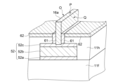
また、前記第1容量電極の第1部分及び第2部分は、平面視において、前記層間絶縁層の開口の側面に沿って配置された前記スペーサーの内側に配置されている。
Claims (7)
- 液晶層と、
画素電極と、
第1配線と、
前記第1配線を覆う層間絶縁層と、
前記層間絶縁層の開口内に埋め込まれ、前記第1配線と電気的に接続された第1部分と、前記層間絶縁層から突出するように配置された第2部分と、を含む第1容量電極と、
前記第1容量電極の前記層間絶縁層から突出した部分を覆うように配置された容量絶縁層と、
前記第1容量電極と前記容量絶縁層を介して配置されるとともに、前記画素電極と電気的に接続された第2容量電極と、
前記層間絶縁層の開口の側面と前記第1容量電極の第1部分との間に配置されたスペーサーと、
を有することを特徴とする電気光学装置。 - 請求項1に記載の電気光学装置であって、
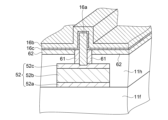
前記第1容量電極の第1部分及び第2部分は、平面視において、前記層間絶縁層の開口の側面に沿って配置された前記スペーサーの内側に配置されていることを特徴とする電気光学装置。 - 請求項1に記載の電気光学装置であって、
前記第1配線と前記第2容量電極との間にストッパー層が配置されていることを特徴とする電気光学装置。 - 請求項3に記載の電気光学装置であって、
前記ストッパー層は、前記層間絶縁層の開口と重なる位置に開口を有し、
前記スペーサーは、前記ストッパー層の開口の側面と前記第1容量電極の第1部分との間に配置されていることを特徴とする電気光学装置。 - 請求項1乃至請求項4のいずれか一項に記載の電気光学装置であって、
前記第1容量電極は、タングステンを含むことを特徴とする電気光学装置。 - 請求項3に記載の電気光学装置であって、
前記第1配線と前記ストッパー層との間に前記層間絶縁層が配置されていることを特徴とする電気光学装置。 - 請求項1乃至請求項6のいずれか一項に記載の電気光学装置を備えることを特徴とする電子機器。
Priority Applications (3)
| Application Number | Priority Date | Filing Date | Title |
|---|---|---|---|
| JP2020117597A JP7476695B2 (ja) | 2020-07-08 | 2020-07-08 | 電気光学装置及び電子機器 |
| CN202110762203.4A CN113917741B (zh) | 2020-07-08 | 2021-07-06 | 电光装置、电子设备以及电光装置的制造方法 |
| US17/369,383 US11480840B2 (en) | 2020-07-08 | 2021-07-07 | Electric optical device, electronic device, and manufacturing method of electric optical device |
Applications Claiming Priority (1)
| Application Number | Priority Date | Filing Date | Title |
|---|---|---|---|
| JP2020117597A JP7476695B2 (ja) | 2020-07-08 | 2020-07-08 | 電気光学装置及び電子機器 |
Publications (3)
| Publication Number | Publication Date |
|---|---|
| JP2022015019A JP2022015019A (ja) | 2022-01-21 |
| JP2022015019A5 JP2022015019A5 (ja) | 2023-05-18 |
| JP7476695B2 true JP7476695B2 (ja) | 2024-05-01 |
Family
ID=79172458
Family Applications (1)
| Application Number | Title | Priority Date | Filing Date |
|---|---|---|---|
| JP2020117597A Active JP7476695B2 (ja) | 2020-07-08 | 2020-07-08 | 電気光学装置及び電子機器 |
Country Status (3)
| Country | Link |
|---|---|
| US (1) | US11480840B2 (ja) |
| JP (1) | JP7476695B2 (ja) |
| CN (1) | CN113917741B (ja) |
Citations (5)
| Publication number | Priority date | Publication date | Assignee | Title |
|---|---|---|---|---|
| JP2002217386A (ja) | 2001-01-19 | 2002-08-02 | Hitachi Ltd | 半導体装置の製造方法 |
| JP2005521205A (ja) | 2002-03-20 | 2005-07-14 | コーニンクレッカ フィリップス エレクトロニクス エヌ ヴィ | アクティブマトリクス表示装置及びその製造方法 |
| JP2011049321A (ja) | 2009-08-26 | 2011-03-10 | Sony Corp | 半導体装置及びその製造方法 |
| JP2016105473A (ja) | 2014-11-21 | 2016-06-09 | 株式会社半導体エネルギー研究所 | 半導体装置および電子機器 |
| US20200212154A1 (en) | 2018-12-28 | 2020-07-02 | Lg Display Co., Ltd. | Display device |
Family Cites Families (12)
| Publication number | Priority date | Publication date | Assignee | Title |
|---|---|---|---|---|
| JP2000171827A (ja) * | 1998-12-03 | 2000-06-23 | Casio Comput Co Ltd | 液晶表示パネル |
| JP3991567B2 (ja) * | 1998-12-28 | 2007-10-17 | セイコーエプソン株式会社 | 電気光学装置及び電子機器 |
| JP3798186B2 (ja) | 1999-06-14 | 2006-07-19 | 富士通株式会社 | 液晶表示基板及びその製造方法、並びに液晶表示装置 |
| JP4023107B2 (ja) * | 2001-05-17 | 2007-12-19 | セイコーエプソン株式会社 | 電気光学装置及びこれを具備する電子機器 |
| JP2005062759A (ja) | 2003-08-20 | 2005-03-10 | Seiko Epson Corp | 基板装置、並びにこれを備えた電気光学装置及び電子機器 |
| JP2006064967A (ja) | 2004-08-26 | 2006-03-09 | Sharp Corp | アクティブマトリクス基板及びそれを用いた容量性表示装置 |
| JP5423462B2 (ja) * | 2010-02-12 | 2014-02-19 | カシオ計算機株式会社 | 液晶表示装置 |
| JP5782676B2 (ja) * | 2010-03-10 | 2015-09-24 | セイコーエプソン株式会社 | 電気光学装置及び電子機器、並びに電気光学装置の製造方法 |
| US9202822B2 (en) * | 2010-12-17 | 2015-12-01 | Semiconductor Energy Laboratory Co., Ltd. | Semiconductor device and manufacturing method thereof |
| JP5919636B2 (ja) * | 2011-04-01 | 2016-05-18 | セイコーエプソン株式会社 | 電気光学装置、電子機器、電気光学装置の製造方法 |
| JP2018136478A (ja) * | 2017-02-23 | 2018-08-30 | セイコーエプソン株式会社 | 電気光学装置、電気光学装置の製造方法、および電子機器 |
| JP6593416B2 (ja) * | 2017-10-23 | 2019-10-23 | セイコーエプソン株式会社 | 電気光学装置および電子機器 |
-
2020
- 2020-07-08 JP JP2020117597A patent/JP7476695B2/ja active Active
-
2021
- 2021-07-06 CN CN202110762203.4A patent/CN113917741B/zh active Active
- 2021-07-07 US US17/369,383 patent/US11480840B2/en active Active
Patent Citations (5)
| Publication number | Priority date | Publication date | Assignee | Title |
|---|---|---|---|---|
| JP2002217386A (ja) | 2001-01-19 | 2002-08-02 | Hitachi Ltd | 半導体装置の製造方法 |
| JP2005521205A (ja) | 2002-03-20 | 2005-07-14 | コーニンクレッカ フィリップス エレクトロニクス エヌ ヴィ | アクティブマトリクス表示装置及びその製造方法 |
| JP2011049321A (ja) | 2009-08-26 | 2011-03-10 | Sony Corp | 半導体装置及びその製造方法 |
| JP2016105473A (ja) | 2014-11-21 | 2016-06-09 | 株式会社半導体エネルギー研究所 | 半導体装置および電子機器 |
| US20200212154A1 (en) | 2018-12-28 | 2020-07-02 | Lg Display Co., Ltd. | Display device |
Also Published As
| Publication number | Publication date |
|---|---|
| US20220011615A1 (en) | 2022-01-13 |
| US11480840B2 (en) | 2022-10-25 |
| CN113917741A (zh) | 2022-01-11 |
| CN113917741B (zh) | 2023-06-27 |
| JP2022015019A (ja) | 2022-01-21 |
Similar Documents
| Publication | Publication Date | Title |
|---|---|---|
| JP2014212191A (ja) | 半導体装置、電気光学装置、半導体装置の製造方法、電気光学装置の製造方法、及び電子機器 | |
| JP2017058537A (ja) | 電気光学装置、電気光学装置の製造方法、および電子機器 | |
| JP2021148813A (ja) | 光学基板、電気光学装置、及び電子機器 | |
| JP7476695B2 (ja) | 電気光学装置及び電子機器 | |
| JP2021184005A (ja) | 電気光学装置、電子機器、電気光学装置の製造方法 | |
| JP7028281B2 (ja) | 電気光学装置、及び電子機器 | |
| JP7435087B2 (ja) | 電気光学装置、及び電子機器 | |
| JP7409236B2 (ja) | 電気光学装置、及び電子機器 | |
| US11204519B2 (en) | Liquid crystal apparatus and electronic device | |
| JP7484222B2 (ja) | 光学基板、電気光学装置、電子機器、及び光学基板の製造方法 | |
| JP6303283B2 (ja) | 半導体装置、電気光学装置、半導体装置の製造方法、及び電子機器 | |
| JP7415725B2 (ja) | 液晶装置、及び電子機器 | |
| JP6205836B2 (ja) | 液晶装置、及び電子機器 | |
| JP2022015457A (ja) | 電気光学装置、電子機器、及び電気光学装置の製造方法 | |
| JP2022007339A (ja) | 電気光学装置、及び電子機器 | |
| JP2017040847A (ja) | 液晶装置、液晶装置の製造方法、及び電子機器 | |
| JP6236827B2 (ja) | 電気光学装置、電気光学装置の製造方法、及び電子機器 | |
| JP2022188878A (ja) | 液晶装置、及び電子機器 | |
| JP2021179490A (ja) | 液晶装置、及び電子機器 | |
| JP2021131508A (ja) | 電気光学装置、及び電子機器 | |
| JP2018050069A (ja) | 半導体装置、電気光学装置、及び電子機器 | |
| JP2012078680A (ja) | 電気光学装置、電気光学装置の製造方法、電子機器 | |
| JP2014026142A (ja) | 液晶装置の製造方法、液晶装置、及び電子機器 | |
| JP2019128518A (ja) | 電気光学装置、電子機器 | |
| JP2018056260A (ja) | 半導体装置および電気光学装置 |
Legal Events
| Date | Code | Title | Description |
|---|---|---|---|
| RD04 | Notification of resignation of power of attorney |
Free format text: JAPANESE INTERMEDIATE CODE: A7424 Effective date: 20210916 |
|
| RD03 | Notification of appointment of power of attorney |
Free format text: JAPANESE INTERMEDIATE CODE: A7423 Effective date: 20211108 |
|
| A521 | Request for written amendment filed |
Free format text: JAPANESE INTERMEDIATE CODE: A523 Effective date: 20230510 |
|
| A621 | Written request for application examination |
Free format text: JAPANESE INTERMEDIATE CODE: A621 Effective date: 20230510 |
|
| A977 | Report on retrieval |
Free format text: JAPANESE INTERMEDIATE CODE: A971007 Effective date: 20231228 |
|
| A131 | Notification of reasons for refusal |
Free format text: JAPANESE INTERMEDIATE CODE: A131 Effective date: 20240116 |
|
| A521 | Request for written amendment filed |
Free format text: JAPANESE INTERMEDIATE CODE: A523 Effective date: 20240124 |
|
| TRDD | Decision of grant or rejection written | ||
| A01 | Written decision to grant a patent or to grant a registration (utility model) |
Free format text: JAPANESE INTERMEDIATE CODE: A01 Effective date: 20240319 |
|
| A61 | First payment of annual fees (during grant procedure) |
Free format text: JAPANESE INTERMEDIATE CODE: A61 Effective date: 20240401 |
|
| R150 | Certificate of patent or registration of utility model |
Ref document number: 7476695 Country of ref document: JP Free format text: JAPANESE INTERMEDIATE CODE: R150 |