JP7302011B2 - 垂直プローブアレイ用のキャリア構造上のプローブ - Google Patents
垂直プローブアレイ用のキャリア構造上のプローブ Download PDFInfo
- Publication number
- JP7302011B2 JP7302011B2 JP2021562102A JP2021562102A JP7302011B2 JP 7302011 B2 JP7302011 B2 JP 7302011B2 JP 2021562102 A JP2021562102 A JP 2021562102A JP 2021562102 A JP2021562102 A JP 2021562102A JP 7302011 B2 JP7302011 B2 JP 7302011B2
- Authority
- JP
- Japan
- Prior art keywords
- probe
- space transformer
- probes
- vertical
- probe array
- Prior art date
- Legal status (The legal status is an assumption and is not a legal conclusion. Google has not performed a legal analysis and makes no representation as to the accuracy of the status listed.)
- Active
Links
- 239000000523 sample Substances 0.000 title claims description 111
- 238000003491 array Methods 0.000 title description 6
- 238000012360 testing method Methods 0.000 claims description 17
- 230000002787 reinforcement Effects 0.000 claims description 6
- 239000000919 ceramic Substances 0.000 claims description 5
- 239000000758 substrate Substances 0.000 claims description 4
- 238000000034 method Methods 0.000 description 6
- 239000002184 metal Substances 0.000 description 5
- 229910052751 metal Inorganic materials 0.000 description 5
- 238000010586 diagram Methods 0.000 description 4
- 239000000463 material Substances 0.000 description 4
- 150000003071 polychlorinated biphenyls Chemical class 0.000 description 4
- 239000002131 composite material Substances 0.000 description 3
- 239000010949 copper Substances 0.000 description 3
- 239000011521 glass Substances 0.000 description 3
- 238000004519 manufacturing process Methods 0.000 description 3
- 150000002739 metals Chemical class 0.000 description 3
- 239000003351 stiffener Substances 0.000 description 3
- 229910001374 Invar Inorganic materials 0.000 description 2
- PXHVJJICTQNCMI-UHFFFAOYSA-N Nickel Chemical compound [Ni] PXHVJJICTQNCMI-UHFFFAOYSA-N 0.000 description 2
- XUIMIQQOPSSXEZ-UHFFFAOYSA-N Silicon Chemical compound [Si] XUIMIQQOPSSXEZ-UHFFFAOYSA-N 0.000 description 2
- 239000000853 adhesive Substances 0.000 description 2
- 230000001070 adhesive effect Effects 0.000 description 2
- 238000005516 engineering process Methods 0.000 description 2
- 230000003014 reinforcing effect Effects 0.000 description 2
- 229910052710 silicon Inorganic materials 0.000 description 2
- 239000010703 silicon Substances 0.000 description 2
- RZVAJINKPMORJF-UHFFFAOYSA-N Acetaminophen Chemical compound CC(=O)NC1=CC=C(O)C=C1 RZVAJINKPMORJF-UHFFFAOYSA-N 0.000 description 1
- RYGMFSIKBFXOCR-UHFFFAOYSA-N Copper Chemical compound [Cu] RYGMFSIKBFXOCR-UHFFFAOYSA-N 0.000 description 1
- 229910052581 Si3N4 Inorganic materials 0.000 description 1
- 239000006094 Zerodur Substances 0.000 description 1
- 230000009471 action Effects 0.000 description 1
- 229910045601 alloy Inorganic materials 0.000 description 1
- 239000000956 alloy Substances 0.000 description 1
- 229910052790 beryllium Inorganic materials 0.000 description 1
- ATBAMAFKBVZNFJ-UHFFFAOYSA-N beryllium atom Chemical compound [Be] ATBAMAFKBVZNFJ-UHFFFAOYSA-N 0.000 description 1
- 239000005352 borofloat Substances 0.000 description 1
- 239000000969 carrier Substances 0.000 description 1
- 238000010276 construction Methods 0.000 description 1
- 229910052802 copper Inorganic materials 0.000 description 1
- KZHJGOXRZJKJNY-UHFFFAOYSA-N dioxosilane;oxo(oxoalumanyloxy)alumane Chemical compound O=[Si]=O.O=[Si]=O.O=[Al]O[Al]=O.O=[Al]O[Al]=O.O=[Al]O[Al]=O KZHJGOXRZJKJNY-UHFFFAOYSA-N 0.000 description 1
- 230000006872 improvement Effects 0.000 description 1
- 238000009434 installation Methods 0.000 description 1
- 230000014759 maintenance of location Effects 0.000 description 1
- 230000007246 mechanism Effects 0.000 description 1
- 229910052863 mullite Inorganic materials 0.000 description 1
- 229910052759 nickel Inorganic materials 0.000 description 1
- 230000008569 process Effects 0.000 description 1
- 239000005297 pyrex Substances 0.000 description 1
- 239000010453 quartz Substances 0.000 description 1
- 229910052703 rhodium Inorganic materials 0.000 description 1
- 239000010948 rhodium Substances 0.000 description 1
- MHOVAHRLVXNVSD-UHFFFAOYSA-N rhodium atom Chemical compound [Rh] MHOVAHRLVXNVSD-UHFFFAOYSA-N 0.000 description 1
- 238000005201 scrubbing Methods 0.000 description 1
- VYPSYNLAJGMNEJ-UHFFFAOYSA-N silicon dioxide Inorganic materials O=[Si]=O VYPSYNLAJGMNEJ-UHFFFAOYSA-N 0.000 description 1
- HQVNEWCFYHHQES-UHFFFAOYSA-N silicon nitride Chemical compound N12[Si]34N5[Si]62N3[Si]51N64 HQVNEWCFYHHQES-UHFFFAOYSA-N 0.000 description 1
Images


Classifications
-
- G—PHYSICS
- G01—MEASURING; TESTING
- G01R—MEASURING ELECTRIC VARIABLES; MEASURING MAGNETIC VARIABLES
- G01R1/00—Details of instruments or arrangements of the types included in groups G01R5/00 - G01R13/00 and G01R31/00
- G01R1/02—General constructional details
- G01R1/06—Measuring leads; Measuring probes
- G01R1/067—Measuring probes
- G01R1/073—Multiple probes
- G01R1/07307—Multiple probes with individual probe elements, e.g. needles, cantilever beams or bump contacts, fixed in relation to each other, e.g. bed of nails fixture or probe card
- G01R1/07314—Multiple probes with individual probe elements, e.g. needles, cantilever beams or bump contacts, fixed in relation to each other, e.g. bed of nails fixture or probe card the body of the probe being perpendicular to test object, e.g. bed of nails or probe with bump contacts on a rigid support
-
- G—PHYSICS
- G01—MEASURING; TESTING
- G01R—MEASURING ELECTRIC VARIABLES; MEASURING MAGNETIC VARIABLES
- G01R1/00—Details of instruments or arrangements of the types included in groups G01R5/00 - G01R13/00 and G01R31/00
- G01R1/02—General constructional details
- G01R1/06—Measuring leads; Measuring probes
- G01R1/067—Measuring probes
- G01R1/06711—Probe needles; Cantilever beams; "Bump" contacts; Replaceable probe pins
- G01R1/06716—Elastic
- G01R1/06727—Cantilever beams
-
- G—PHYSICS
- G01—MEASURING; TESTING
- G01R—MEASURING ELECTRIC VARIABLES; MEASURING MAGNETIC VARIABLES
- G01R1/00—Details of instruments or arrangements of the types included in groups G01R5/00 - G01R13/00 and G01R31/00
- G01R1/02—General constructional details
- G01R1/06—Measuring leads; Measuring probes
- G01R1/067—Measuring probes
- G01R1/06711—Probe needles; Cantilever beams; "Bump" contacts; Replaceable probe pins
- G01R1/06733—Geometry aspects
- G01R1/06738—Geometry aspects related to tip portion
-
- G—PHYSICS
- G01—MEASURING; TESTING
- G01R—MEASURING ELECTRIC VARIABLES; MEASURING MAGNETIC VARIABLES
- G01R1/00—Details of instruments or arrangements of the types included in groups G01R5/00 - G01R13/00 and G01R31/00
- G01R1/02—General constructional details
- G01R1/06—Measuring leads; Measuring probes
- G01R1/067—Measuring probes
- G01R1/073—Multiple probes
- G01R1/07307—Multiple probes with individual probe elements, e.g. needles, cantilever beams or bump contacts, fixed in relation to each other, e.g. bed of nails fixture or probe card
- G01R1/07357—Multiple probes with individual probe elements, e.g. needles, cantilever beams or bump contacts, fixed in relation to each other, e.g. bed of nails fixture or probe card with flexible bodies, e.g. buckling beams
-
- G—PHYSICS
- G01—MEASURING; TESTING
- G01R—MEASURING ELECTRIC VARIABLES; MEASURING MAGNETIC VARIABLES
- G01R1/00—Details of instruments or arrangements of the types included in groups G01R5/00 - G01R13/00 and G01R31/00
- G01R1/02—General constructional details
- G01R1/06—Measuring leads; Measuring probes
- G01R1/067—Measuring probes
- G01R1/073—Multiple probes
- G01R1/07307—Multiple probes with individual probe elements, e.g. needles, cantilever beams or bump contacts, fixed in relation to each other, e.g. bed of nails fixture or probe card
- G01R1/07364—Multiple probes with individual probe elements, e.g. needles, cantilever beams or bump contacts, fixed in relation to each other, e.g. bed of nails fixture or probe card with provisions for altering position, number or connection of probe tips; Adapting to differences in pitch
- G01R1/07378—Multiple probes with individual probe elements, e.g. needles, cantilever beams or bump contacts, fixed in relation to each other, e.g. bed of nails fixture or probe card with provisions for altering position, number or connection of probe tips; Adapting to differences in pitch using an intermediate adapter, e.g. space transformers
Landscapes
- Physics & Mathematics (AREA)
- General Physics & Mathematics (AREA)
- Geometry (AREA)
- Engineering & Computer Science (AREA)
- Power Engineering (AREA)
- Measuring Leads Or Probes (AREA)
- Testing Or Measuring Of Semiconductors Or The Like (AREA)
- Testing Of Individual Semiconductor Devices (AREA)
Description
Claims (8)
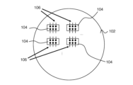
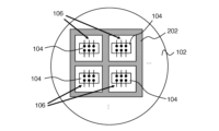
- 電気デバイスを試験するためのプローブアレイであって、
スペーストランスフォーマと、
前記スペーストランスフォーマ上、または前記スペーストランスフォーマに近接して配置された2以上のプローブキャリアプレートとを備え、
前記プローブキャリアプレートのそれぞれは、その上に配置された2以上の垂直プローブを有し、
前記垂直プローブのそれぞれは、前記スペーストランスフォーマに電気的に接触する第1の可撓性部材を有し、
前記垂直プローブのそれぞれは、試験中のデバイスに一時的に電気的に接触するように構成された第2の可撓性部材を有し、
前記垂直プローブのそれぞれは、2以上の前記プローブキャリアプレートのなかの対応する1つに取り付けられたプローブ本体を含み、
前記垂直プローブのそれぞれは、その垂直プローブの前記プローブ本体、前記第1の可撓性部材、及び前記第2の可撓性部材を一体的に有する1個部品であることを特徴とするプローブアレイ。 - 前記スペーストランスフォーマに取り付けられた機械的補強部材をさらに備えることを特徴とする請求項1に記載のプローブアレイ。
- 前記プローブキャリアプレートは前記スペーストランスフォーマ上に配置され、
前記機械的補強部材は、前記スペーストランスフォーマの熱膨張と、前記スペーストランスフォーマの平坦度からの逸脱との両方を制限するように構成されることを特徴とする請求項2に記載のプローブアレイ。 - 前記機械的補強部材は、前記スペーストランスフォーマに接合部またはスタンドオフを介して取り付けられ、
前記プローブキャリアプレートは前記機械的補強部材上に配置され、
前記垂直プローブの前記第1の可撓性部材は、前記スペーストランスフォーマの熱膨張と、前記スペーストランスフォーマの平坦度からの逸脱との両方に適応するように構成されることを特徴とする請求項2に記載のプローブアレイ。 - 前記垂直プローブは2次元MEMSプローブであることを特徴とする請求項1に記載のプローブアレイ。
- 前記スペーストランスフォーマはセラミック基板を含むことを特徴とする請求項1に記載のプローブアレイ。
- 前記スペーストランスフォーマはプリント基板を含むことを特徴とする請求項1に記載のプローブアレイ。
- 2以上の前記垂直プローブの先端部の位置のばらつきが、25μm以下となる程度まで平坦であることを特徴とする請求項1に記載のプローブアレイ。
Applications Claiming Priority (3)
| Application Number | Priority Date | Filing Date | Title |
|---|---|---|---|
| US201962839480P | 2019-04-26 | 2019-04-26 | |
| US62/839,480 | 2019-04-26 | ||
| PCT/US2020/030031 WO2020220012A1 (en) | 2019-04-26 | 2020-04-27 | Probe on carrier architecture for vertical probe arrays |
Publications (2)
| Publication Number | Publication Date |
|---|---|
| JP2022529486A JP2022529486A (ja) | 2022-06-22 |
| JP7302011B2 true JP7302011B2 (ja) | 2023-07-03 |
Family
ID=72922512
Family Applications (1)
| Application Number | Title | Priority Date | Filing Date |
|---|---|---|---|
| JP2021562102A Active JP7302011B2 (ja) | 2019-04-26 | 2020-04-27 | 垂直プローブアレイ用のキャリア構造上のプローブ |
Country Status (4)
| Country | Link |
|---|---|
| US (1) | US11293947B2 (ja) |
| EP (1) | EP3959524A4 (ja) |
| JP (1) | JP7302011B2 (ja) |
| WO (1) | WO2020220012A1 (ja) |
Families Citing this family (3)
| Publication number | Priority date | Publication date | Assignee | Title |
|---|---|---|---|---|
| TWI797004B (zh) * | 2022-04-29 | 2023-03-21 | 中華精測科技股份有限公司 | 懸臂式探針卡及其承載座 |
| TWI792996B (zh) * | 2022-04-29 | 2023-02-11 | 中華精測科技股份有限公司 | 懸臂式探針卡裝置及其彈臂型探針 |
| US12498398B2 (en) | 2023-02-23 | 2025-12-16 | Snap-On Incorporated | Electrical testing device with probe having an adjustable angle |
Citations (4)
| Publication number | Priority date | Publication date | Assignee | Title |
|---|---|---|---|---|
| JP2007024555A (ja) | 2005-07-13 | 2007-02-01 | Tokyo Electron Ltd | プローブカード |
| JP2008281564A (ja) | 2007-05-11 | 2008-11-20 | Amst Co Ltd | プローブカード及びその製造方法 |
| US20090237099A1 (en) | 2008-03-20 | 2009-09-24 | Touchdown Technologies, Inc. | Probe card substrate with bonded via |
| JP2011106980A (ja) | 2009-11-18 | 2011-06-02 | Advantest Corp | プローブカード |
Family Cites Families (22)
| Publication number | Priority date | Publication date | Assignee | Title |
|---|---|---|---|---|
| JPS6180067A (ja) * | 1984-09-21 | 1986-04-23 | インタ−ナショナル ビジネス マシ−ンズ コ−ポレ−ション | テスト・プロ−ブ装置 |
| JPH0766252A (ja) * | 1993-08-25 | 1995-03-10 | Tokyo Electron Ltd | プローブカード |
| US7064566B2 (en) | 1993-11-16 | 2006-06-20 | Formfactor, Inc. | Probe card assembly and kit |
| US5806181A (en) | 1993-11-16 | 1998-09-15 | Formfactor, Inc. | Contact carriers (tiles) for populating larger substrates with spring contacts |
| JPH07321168A (ja) * | 1994-05-27 | 1995-12-08 | Tokyo Electron Ltd | プローブカード |
| US6066957A (en) | 1997-09-11 | 2000-05-23 | Delaware Capital Formation, Inc. | Floating spring probe wireless test fixture |
| US6419500B1 (en) * | 1999-03-08 | 2002-07-16 | Kulicke & Soffa Investment, Inc. | Probe assembly having floatable buckling beam probes and apparatus for abrading the same |
| US7349223B2 (en) | 2000-05-23 | 2008-03-25 | Nanonexus, Inc. | Enhanced compliant probe card systems having improved planarity |
| US6426638B1 (en) | 2000-05-02 | 2002-07-30 | Decision Track Llc | Compliant probe apparatus |
| US6870382B2 (en) | 2002-05-03 | 2005-03-22 | Texas Instruments Incorporated | System and method for evaluating the planarity and parallelism of an array of probe tips |
| US6965244B2 (en) * | 2002-05-08 | 2005-11-15 | Formfactor, Inc. | High performance probe system |
| US7084650B2 (en) | 2002-12-16 | 2006-08-01 | Formfactor, Inc. | Apparatus and method for limiting over travel in a probe card assembly |
| US7071715B2 (en) * | 2004-01-16 | 2006-07-04 | Formfactor, Inc. | Probe card configuration for low mechanical flexural strength electrical routing substrates |
| US7459795B2 (en) * | 2004-08-19 | 2008-12-02 | Formfactor, Inc. | Method to build a wirebond probe card in a many at a time fashion |
| US7876087B2 (en) | 2006-09-12 | 2011-01-25 | Innoconnex, Inc. | Probe card repair using coupons with spring contacts and separate atachment points |
| KR100791945B1 (ko) * | 2007-08-23 | 2008-01-04 | (주)기가레인 | 프로브 카드 |
| US7960989B2 (en) * | 2008-12-03 | 2011-06-14 | Formfactor, Inc. | Mechanical decoupling of a probe card assembly to improve thermal response |
| US20100176831A1 (en) * | 2009-01-14 | 2010-07-15 | Palcisko William M | Probe Test Card with Flexible Interconnect Structure |
| WO2014182633A1 (en) | 2013-05-06 | 2014-11-13 | Formfactor | A probe card assembly for testing electronic devices |
| US9459288B2 (en) * | 2014-01-16 | 2016-10-04 | Infineon Technologies Ag | Wide interposer for an electronic testing system |
| SG11201607219PA (en) * | 2014-03-06 | 2016-09-29 | Technoprobe Spa | Probe card for a testing apparatus of electronic devices, particularly for extreme temperature applications |
| KR102422188B1 (ko) | 2017-08-30 | 2022-07-15 | 폼팩터, 인크. | 타일링된 멤브레인 스페이스 트랜스포머를 갖는 수직형 프로브 어레이 |
-
2020
- 2020-04-27 JP JP2021562102A patent/JP7302011B2/ja active Active
- 2020-04-27 WO PCT/US2020/030031 patent/WO2020220012A1/en not_active Ceased
- 2020-04-27 US US16/858,976 patent/US11293947B2/en active Active
- 2020-04-27 EP EP20794523.9A patent/EP3959524A4/en active Pending
Patent Citations (4)
| Publication number | Priority date | Publication date | Assignee | Title |
|---|---|---|---|---|
| JP2007024555A (ja) | 2005-07-13 | 2007-02-01 | Tokyo Electron Ltd | プローブカード |
| JP2008281564A (ja) | 2007-05-11 | 2008-11-20 | Amst Co Ltd | プローブカード及びその製造方法 |
| US20090237099A1 (en) | 2008-03-20 | 2009-09-24 | Touchdown Technologies, Inc. | Probe card substrate with bonded via |
| JP2011106980A (ja) | 2009-11-18 | 2011-06-02 | Advantest Corp | プローブカード |
Also Published As
| Publication number | Publication date |
|---|---|
| EP3959524A1 (en) | 2022-03-02 |
| WO2020220012A1 (en) | 2020-10-29 |
| US20200341030A1 (en) | 2020-10-29 |
| EP3959524A4 (en) | 2023-01-18 |
| JP2022529486A (ja) | 2022-06-22 |
| US11293947B2 (en) | 2022-04-05 |
Similar Documents
| Publication | Publication Date | Title |
|---|---|---|
| US7349223B2 (en) | Enhanced compliant probe card systems having improved planarity | |
| JP7302011B2 (ja) | 垂直プローブアレイ用のキャリア構造上のプローブ | |
| JP6513639B2 (ja) | 電子デバイスを試験するためのプローブカードアセンブリ | |
| KR100791945B1 (ko) | 프로브 카드 | |
| US10509056B2 (en) | Probe card for a testing apparatus of electronic devices, particularly for extreme temperature applications | |
| US20120023730A1 (en) | Construction structures and manufacturing processes for integrated circuit wafer probe card assemblies | |
| TW201839408A (zh) | 電子裝置的測試設備的探針卡 | |
| TWI400448B (zh) | Electrical signal connection device | |
| KR20100055537A (ko) | 테스트 장치와 함께 사용하기 위한 보강재 어셈블리 | |
| TW200305723A (en) | Electroconductive contact probe holder | |
| US20240012028A1 (en) | Large probe card for testing electronic devices and related manufacturing method | |
| KR20230109173A (ko) | 전자 소자를 테스트하기 위한 대형 프로브 헤드 및 관련 제조방법 | |
| JP4721099B2 (ja) | 電気信号接続装置及びこれを用いたプローブ組立体並びにプローバ装置 | |
| CN112771387A (zh) | 测量装置 | |
| WO2012099572A1 (en) | Stiffener plate for a probecard and method | |
| KR100932990B1 (ko) | 프로브 카드 조립체 | |
| TW201825917A (zh) | 具有晶粒級及接針級順應性之探針卡總成及其相關聯系統與方法 | |
| JP2004274010A (ja) | プローバ装置 | |
| TW202411663A (zh) | 具有改善溫度控制的探針卡 | |
| KR20250019644A (ko) | 전자 소자 테스트 장치용 프로브 카드 및 그에 대응하는 스페이스 트랜스포머 | |
| JP4962929B2 (ja) | プローバ装置及びこれに用いるプローブ組立体 | |
| KR101010675B1 (ko) | 공간 변환기와 이를 포함하는 프로브 카드 | |
| KR101306839B1 (ko) | 신호 분기 기판을 갖는 프로브 카드 | |
| JP5079890B2 (ja) | 積層基板及びプローブカード | |
| TW202210838A (zh) | 接觸端子、檢查治具、檢查裝置、及製造方法 |
Legal Events
| Date | Code | Title | Description |
|---|---|---|---|
| A621 | Written request for application examination |
Free format text: JAPANESE INTERMEDIATE CODE: A621 Effective date: 20220114 |
|
| A131 | Notification of reasons for refusal |
Free format text: JAPANESE INTERMEDIATE CODE: A131 Effective date: 20221206 |
|
| A601 | Written request for extension of time |
Free format text: JAPANESE INTERMEDIATE CODE: A601 Effective date: 20230303 |
|
| A521 | Request for written amendment filed |
Free format text: JAPANESE INTERMEDIATE CODE: A523 Effective date: 20230502 |
|
| TRDD | Decision of grant or rejection written | ||
| A01 | Written decision to grant a patent or to grant a registration (utility model) |
Free format text: JAPANESE INTERMEDIATE CODE: A01 Effective date: 20230523 |
|
| A61 | First payment of annual fees (during grant procedure) |
Free format text: JAPANESE INTERMEDIATE CODE: A61 Effective date: 20230621 |
|
| R150 | Certificate of patent or registration of utility model |
Ref document number: 7302011 Country of ref document: JP Free format text: JAPANESE INTERMEDIATE CODE: R150 |