JP7236844B2 - 表示装置、及びその製造方法 - Google Patents
表示装置、及びその製造方法 Download PDFInfo
- Publication number
- JP7236844B2 JP7236844B2 JP2018212367A JP2018212367A JP7236844B2 JP 7236844 B2 JP7236844 B2 JP 7236844B2 JP 2018212367 A JP2018212367 A JP 2018212367A JP 2018212367 A JP2018212367 A JP 2018212367A JP 7236844 B2 JP7236844 B2 JP 7236844B2
- Authority
- JP
- Japan
- Prior art keywords
- pixel
- vapor deposition
- pixel electrode
- substrate
- convex portion
- Prior art date
- Legal status (The legal status is an assumption and is not a legal conclusion. Google has not performed a legal analysis and makes no representation as to the accuracy of the status listed.)
- Active
Links
- 238000004519 manufacturing process Methods 0.000 title claims description 12
- 238000007740 vapor deposition Methods 0.000 claims description 96
- 239000000758 substrate Substances 0.000 claims description 94
- 239000010410 layer Substances 0.000 claims description 83
- 125000006850 spacer group Chemical group 0.000 claims description 21
- 239000012044 organic layer Substances 0.000 claims description 20
- 230000001747 exhibiting effect Effects 0.000 claims description 8
- 239000010408 film Substances 0.000 description 64
- 239000011368 organic material Substances 0.000 description 58
- 238000000151 deposition Methods 0.000 description 26
- 230000008021 deposition Effects 0.000 description 25
- 238000005401 electroluminescence Methods 0.000 description 18
- 239000003086 colorant Substances 0.000 description 13
- 238000000034 method Methods 0.000 description 12
- 230000015572 biosynthetic process Effects 0.000 description 10
- 239000000463 material Substances 0.000 description 10
- 239000003990 capacitor Substances 0.000 description 9
- 229910052751 metal Inorganic materials 0.000 description 7
- 239000002184 metal Substances 0.000 description 7
- 239000004065 semiconductor Substances 0.000 description 6
- 238000005019 vapor deposition process Methods 0.000 description 6
- 229910052581 Si3N4 Inorganic materials 0.000 description 5
- 230000004048 modification Effects 0.000 description 5
- 238000012986 modification Methods 0.000 description 5
- HQVNEWCFYHHQES-UHFFFAOYSA-N silicon nitride Chemical compound N12[Si]34N5[Si]62N3[Si]51N64 HQVNEWCFYHHQES-UHFFFAOYSA-N 0.000 description 5
- 238000010586 diagram Methods 0.000 description 4
- 229920001721 polyimide Polymers 0.000 description 4
- 230000008569 process Effects 0.000 description 4
- 239000011347 resin Substances 0.000 description 4
- 229920005989 resin Polymers 0.000 description 4
- 238000003860 storage Methods 0.000 description 4
- 229920000178 Acrylic resin Polymers 0.000 description 3
- 239000004925 Acrylic resin Substances 0.000 description 3
- 239000004642 Polyimide Substances 0.000 description 3
- VYPSYNLAJGMNEJ-UHFFFAOYSA-N Silicium dioxide Chemical compound O=[Si]=O VYPSYNLAJGMNEJ-UHFFFAOYSA-N 0.000 description 3
- 238000004040 coloring Methods 0.000 description 3
- 238000005137 deposition process Methods 0.000 description 3
- 239000012535 impurity Substances 0.000 description 3
- 229910052814 silicon oxide Inorganic materials 0.000 description 3
- 230000007547 defect Effects 0.000 description 2
- 230000000694 effects Effects 0.000 description 2
- 239000011521 glass Substances 0.000 description 2
- 239000011810 insulating material Substances 0.000 description 2
- 239000011159 matrix material Substances 0.000 description 2
- 238000007789 sealing Methods 0.000 description 2
- 239000010409 thin film Substances 0.000 description 2
- 239000004593 Epoxy Substances 0.000 description 1
- BQCADISMDOOEFD-UHFFFAOYSA-N Silver Chemical compound [Ag] BQCADISMDOOEFD-UHFFFAOYSA-N 0.000 description 1
- NIXOWILDQLNWCW-UHFFFAOYSA-N acrylic acid group Chemical group C(C=C)(=O)O NIXOWILDQLNWCW-UHFFFAOYSA-N 0.000 description 1
- 230000004888 barrier function Effects 0.000 description 1
- 230000005540 biological transmission Effects 0.000 description 1
- 238000000576 coating method Methods 0.000 description 1
- 239000004020 conductor Substances 0.000 description 1
- 230000006866 deterioration Effects 0.000 description 1
- 230000002542 deteriorative effect Effects 0.000 description 1
- 238000005530 etching Methods 0.000 description 1
- 239000000945 filler Substances 0.000 description 1
- AMGQUBHHOARCQH-UHFFFAOYSA-N indium;oxotin Chemical compound [In].[Sn]=O AMGQUBHHOARCQH-UHFFFAOYSA-N 0.000 description 1
- 229910010272 inorganic material Inorganic materials 0.000 description 1
- 239000011147 inorganic material Substances 0.000 description 1
- 239000011229 interlayer Substances 0.000 description 1
- 230000007246 mechanism Effects 0.000 description 1
- 238000010422 painting Methods 0.000 description 1
- 230000000149 penetrating effect Effects 0.000 description 1
- -1 polyethylene terephthalate Polymers 0.000 description 1
- 229920000139 polyethylene terephthalate Polymers 0.000 description 1
- 239000005020 polyethylene terephthalate Substances 0.000 description 1
- 239000009719 polyimide resin Substances 0.000 description 1
- 230000009467 reduction Effects 0.000 description 1
- 229910052709 silver Inorganic materials 0.000 description 1
- 239000004332 silver Substances 0.000 description 1
- YVTHLONGBIQYBO-UHFFFAOYSA-N zinc indium(3+) oxygen(2-) Chemical compound [O--].[Zn++].[In+3] YVTHLONGBIQYBO-UHFFFAOYSA-N 0.000 description 1
Images


Classifications
-
- H—ELECTRICITY
- H10—SEMICONDUCTOR DEVICES; ELECTRIC SOLID-STATE DEVICES NOT OTHERWISE PROVIDED FOR
- H10K—ORGANIC ELECTRIC SOLID-STATE DEVICES
- H10K59/00—Integrated devices, or assemblies of multiple devices, comprising at least one organic light-emitting element covered by group H10K50/00
- H10K59/30—Devices specially adapted for multicolour light emission
- H10K59/35—Devices specially adapted for multicolour light emission comprising red-green-blue [RGB] subpixels
-
- G—PHYSICS
- G09—EDUCATION; CRYPTOGRAPHY; DISPLAY; ADVERTISING; SEALS
- G09F—DISPLAYING; ADVERTISING; SIGNS; LABELS OR NAME-PLATES; SEALS
- G09F9/00—Indicating arrangements for variable information in which the information is built-up on a support by selection or combination of individual elements
- G09F9/30—Indicating arrangements for variable information in which the information is built-up on a support by selection or combination of individual elements in which the desired character or characters are formed by combining individual elements
-
- H—ELECTRICITY
- H05—ELECTRIC TECHNIQUES NOT OTHERWISE PROVIDED FOR
- H05B—ELECTRIC HEATING; ELECTRIC LIGHT SOURCES NOT OTHERWISE PROVIDED FOR; CIRCUIT ARRANGEMENTS FOR ELECTRIC LIGHT SOURCES, IN GENERAL
- H05B33/00—Electroluminescent light sources
- H05B33/10—Apparatus or processes specially adapted to the manufacture of electroluminescent light sources
-
- H—ELECTRICITY
- H05—ELECTRIC TECHNIQUES NOT OTHERWISE PROVIDED FOR
- H05B—ELECTRIC HEATING; ELECTRIC LIGHT SOURCES NOT OTHERWISE PROVIDED FOR; CIRCUIT ARRANGEMENTS FOR ELECTRIC LIGHT SOURCES, IN GENERAL
- H05B33/00—Electroluminescent light sources
- H05B33/12—Light sources with substantially two-dimensional radiating surfaces
- H05B33/22—Light sources with substantially two-dimensional radiating surfaces characterised by the chemical or physical composition or the arrangement of auxiliary dielectric or reflective layers
-
- H—ELECTRICITY
- H05—ELECTRIC TECHNIQUES NOT OTHERWISE PROVIDED FOR
- H05B—ELECTRIC HEATING; ELECTRIC LIGHT SOURCES NOT OTHERWISE PROVIDED FOR; CIRCUIT ARRANGEMENTS FOR ELECTRIC LIGHT SOURCES, IN GENERAL
- H05B33/00—Electroluminescent light sources
- H05B33/12—Light sources with substantially two-dimensional radiating surfaces
- H05B33/26—Light sources with substantially two-dimensional radiating surfaces characterised by the composition or arrangement of the conductive material used as an electrode
-
- H—ELECTRICITY
- H10—SEMICONDUCTOR DEVICES; ELECTRIC SOLID-STATE DEVICES NOT OTHERWISE PROVIDED FOR
- H10K—ORGANIC ELECTRIC SOLID-STATE DEVICES
- H10K50/00—Organic light-emitting devices
- H10K50/10—OLEDs or polymer light-emitting diodes [PLED]
- H10K50/11—OLEDs or polymer light-emitting diodes [PLED] characterised by the electroluminescent [EL] layers
- H10K50/125—OLEDs or polymer light-emitting diodes [PLED] characterised by the electroluminescent [EL] layers specially adapted for multicolour light emission, e.g. for emitting white light
-
- H—ELECTRICITY
- H10—SEMICONDUCTOR DEVICES; ELECTRIC SOLID-STATE DEVICES NOT OTHERWISE PROVIDED FOR
- H10K—ORGANIC ELECTRIC SOLID-STATE DEVICES
- H10K59/00—Integrated devices, or assemblies of multiple devices, comprising at least one organic light-emitting element covered by group H10K50/00
- H10K59/10—OLED displays
- H10K59/12—Active-matrix OLED [AMOLED] displays
- H10K59/1201—Manufacture or treatment
-
- H—ELECTRICITY
- H10—SEMICONDUCTOR DEVICES; ELECTRIC SOLID-STATE DEVICES NOT OTHERWISE PROVIDED FOR
- H10K—ORGANIC ELECTRIC SOLID-STATE DEVICES
- H10K59/00—Integrated devices, or assemblies of multiple devices, comprising at least one organic light-emitting element covered by group H10K50/00
- H10K59/10—OLED displays
- H10K59/12—Active-matrix OLED [AMOLED] displays
- H10K59/122—Pixel-defining structures or layers, e.g. banks
-
- H—ELECTRICITY
- H10—SEMICONDUCTOR DEVICES; ELECTRIC SOLID-STATE DEVICES NOT OTHERWISE PROVIDED FOR
- H10K—ORGANIC ELECTRIC SOLID-STATE DEVICES
- H10K59/00—Integrated devices, or assemblies of multiple devices, comprising at least one organic light-emitting element covered by group H10K50/00
- H10K59/30—Devices specially adapted for multicolour light emission
- H10K59/35—Devices specially adapted for multicolour light emission comprising red-green-blue [RGB] subpixels
- H10K59/352—Devices specially adapted for multicolour light emission comprising red-green-blue [RGB] subpixels the areas of the RGB subpixels being different
-
- H—ELECTRICITY
- H10—SEMICONDUCTOR DEVICES; ELECTRIC SOLID-STATE DEVICES NOT OTHERWISE PROVIDED FOR
- H10K—ORGANIC ELECTRIC SOLID-STATE DEVICES
- H10K71/00—Manufacture or treatment specially adapted for the organic devices covered by this subclass
-
- H—ELECTRICITY
- H10—SEMICONDUCTOR DEVICES; ELECTRIC SOLID-STATE DEVICES NOT OTHERWISE PROVIDED FOR
- H10K—ORGANIC ELECTRIC SOLID-STATE DEVICES
- H10K71/00—Manufacture or treatment specially adapted for the organic devices covered by this subclass
- H10K71/10—Deposition of organic active material
- H10K71/16—Deposition of organic active material using physical vapour deposition [PVD], e.g. vacuum deposition or sputtering
- H10K71/166—Deposition of organic active material using physical vapour deposition [PVD], e.g. vacuum deposition or sputtering using selective deposition, e.g. using a mask
Description
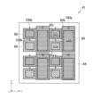
図1は実施形態に係る有機EL表示装置2の概略の構成を示す模式図である。有機EL表示装置2は、画像を表示する表示部である画素アレイ部4と、当該画素アレイ部を駆動する駆動部とを備える。有機EL表示装置2はガラス基板や可撓性を有した樹脂フィルムなどからなる基材の上に薄膜トランジスタ(thin film transistor:TFT)やOLEDなどの積層構造を形成されている。
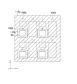
第1の実施形態では、R画素52r、G画素52g、B画素52bが表示領域にストライプ配列される例を説明した。しかし、本発明はストライプ配列以外の画素配列を有する表示装置にも適用することができる。
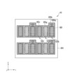
(1)有機材料層85の蒸着に関し、2種類の凸部100のうち低い方を蒸着マスクのスペーサーとして用い、かつ最初に蒸着処理を行う画素を先行蒸着画素、また、複数種類の画素のうち先行蒸着画素の後に2種類の凸部100のうち高い方をスペーサーとして用いて蒸着処理を行う画素を後続蒸着画素と呼ぶことにする。上述の実施形態ではB画素を先行蒸着画素、G画素及びR画素を後続蒸着画素とした。しかし、複数種類の画素のうちいずれの1種類を先行蒸着画素とするかは、本発明の趣旨からは基本的には任意であり、また、後続蒸着画素同士での蒸着の順序も基本的に任意に定めることができる。
Claims (5)
- 複数の画素からなる画像を表示する表示部を形成される基板と、
それぞれ前記画素に対応して前記基板の前記表示部の表示領域の表面に設けられた第1の画素電極及び第2の画素電極と、
それぞれ前記画素間の境界領域に設けられた前記基板の前記表示領域の表面の第1の凸部及び第2の凸部と、
第1の発光色を呈する層を含み前記第1の画素電極に積層された第1の有機層、及び第2の発光色を呈する層を含み前記第2の画素電極に積層された第2の有機層と、を有し、
前記第1の画素電極上に形成された前記第1の有機層が発光する発光領域の面積は、前記第2の画素電極上に形成された前記第2の有機層が発光する発光領域の面積よりも大きく、
前記第1の有機層はさらに前記凸部のうち前記第1の凸部のみを覆うように設けられ、
前記第2の有機層は前記第1の凸部及び前記第2の凸部のいずれも覆わないように設けられ、
前記第1の凸部の頂点は前記第2の凸部の頂点よりも高いこと、
を特徴とする表示装置。 - 前記画素の周囲に形成され、前記画素電極の端部を覆うとともに、前記画素電極の上面を露出する開口部を有するバンクを有し、
前記第1の凸部及び前記第2の凸部は前記バンク上に設けられること、
を特徴とする請求項1に記載の表示装置。 - 複数の画素からなる画像を表示する表示部を形成される基板であって、当該基板の前記表示部の表示領域の表面に、それぞれ前記画素に対応して設けられた第1の画素電極及び第2の画素電極と、前記画素間の境界領域に設けられた第1の凸部及び第2の凸部とを有する基板を準備する工程と、
前記基板における前記第1の画素電極と前記第1の凸部とに対向する領域に開口部を有し、かつ前記第2の凸部に対向する領域に遮蔽部を有した第1の蒸着マスクを、前記基板上に配置する工程と、
前記第1の蒸着マスクを介した蒸着処理により、前記第1の画素電極及び前記第1の凸部を覆い、かつ前記第2の凸部を覆わないように、第1の発光色を呈する層を含む第1の有機層を形成する工程と、
前記基板における前記第2の画素電極に対向する領域に開口部を有し、かつ前記第1の凸部及び前記第2の凸部に対向する領域に遮蔽部を有した第2の蒸着マスクを、前記基板上に配置する工程と、
前記第2の蒸着マスクを介した蒸着処理により、前記第2の画素電極を覆い、かつ前記第1の凸部及び前記第2の凸部を覆わないように、第2の発光色を呈する層を含む第2の有機層を形成する工程と、
を有し、
前記第1の画素電極上に形成された前記第1の有機層が発光する発光領域の面積は、前記第2の画素電極上に形成された前記第2の有機層が発光する発光領域の面積よりも大きくなるように形成され、
前記第1の凸部の頂点は前記第2の凸部の頂点よりも高く、
前記第1の蒸着マスクは前記第2の凸部をスペーサーとして前記基板上に配置され、
前記第2の蒸着マスクは前記第1の凸部をスペーサーとして前記基板上に配置されること、
を特徴とする表示装置の製造方法。 - 前記第1の蒸着マスクはさらに、前記基板における前記第2の画素電極に対向する領域に遮蔽部を有し、
前記第2の蒸着マスクはさらに、前記基板における前記第1の画素電極に対向する領域に遮蔽部を有すること、
を特徴とする請求項3に記載の表示装置の製造方法。 - 前記第2の有機層は前記第1の有機層よりも後に形成されること、を特徴とする請求項3に記載の表示装置の製造方法。
Priority Applications (5)
| Application Number | Priority Date | Filing Date | Title |
|---|---|---|---|
| JP2018212367A JP7236844B2 (ja) | 2018-11-12 | 2018-11-12 | 表示装置、及びその製造方法 |
| KR1020217013866A KR102615044B1 (ko) | 2018-11-12 | 2019-09-25 | 표시 장치 및 그 제조 방법 |
| CN201980074446.XA CN113170551A (zh) | 2018-11-12 | 2019-09-25 | 显示装置及其制造方法 |
| PCT/JP2019/037575 WO2020100441A1 (ja) | 2018-11-12 | 2019-09-25 | 表示装置、及びその製造方法 |
| US17/246,764 US11943971B2 (en) | 2018-11-12 | 2021-05-03 | OLED with one color emitting layer on a convex portion |
Applications Claiming Priority (1)
| Application Number | Priority Date | Filing Date | Title |
|---|---|---|---|
| JP2018212367A JP7236844B2 (ja) | 2018-11-12 | 2018-11-12 | 表示装置、及びその製造方法 |
Publications (3)
| Publication Number | Publication Date |
|---|---|
| JP2020080224A JP2020080224A (ja) | 2020-05-28 |
| JP2020080224A5 JP2020080224A5 (ja) | 2021-12-16 |
| JP7236844B2 true JP7236844B2 (ja) | 2023-03-10 |
Family
ID=70731816
Family Applications (1)
| Application Number | Title | Priority Date | Filing Date |
|---|---|---|---|
| JP2018212367A Active JP7236844B2 (ja) | 2018-11-12 | 2018-11-12 | 表示装置、及びその製造方法 |
Country Status (5)
| Country | Link |
|---|---|
| US (1) | US11943971B2 (ja) |
| JP (1) | JP7236844B2 (ja) |
| KR (1) | KR102615044B1 (ja) |
| CN (1) | CN113170551A (ja) |
| WO (1) | WO2020100441A1 (ja) |
Families Citing this family (3)
| Publication number | Priority date | Publication date | Assignee | Title |
|---|---|---|---|---|
| WO2020158566A1 (ja) * | 2019-01-31 | 2020-08-06 | 大日本印刷株式会社 | 蒸着マスク群、電子デバイスの製造方法及び電子デバイス |
| WO2022224398A1 (ja) * | 2021-04-22 | 2022-10-27 | シャープディスプレイテクノロジー株式会社 | 表示装置及び表示装置の製造方法 |
| CN115568250A (zh) * | 2022-08-30 | 2023-01-03 | 惠科股份有限公司 | 一种屏内指纹显示屏及其制造方法、显示装置 |
Citations (7)
| Publication number | Priority date | Publication date | Assignee | Title |
|---|---|---|---|---|
| JP2006086504A (ja) | 2004-09-16 | 2006-03-30 | Lg Phillips Lcd Co Ltd | 有機電界発光素子及びその製造方法 |
| JP2011100553A (ja) | 2009-11-04 | 2011-05-19 | Seiko Epson Corp | 有機el装置、有機el装置の製造方法、電子機器 |
| JP2011170981A (ja) | 2010-02-16 | 2011-09-01 | Toppan Printing Co Ltd | 有機エレクトロルミネッセンス素子及びその製造方法 |
| JP2011181305A (ja) | 2010-03-01 | 2011-09-15 | Toppan Printing Co Ltd | 有機エレクトロルミネッセンス素子及びその製造方法 |
| JP2013089475A (ja) | 2011-10-19 | 2013-05-13 | Canon Inc | 発光表示装置及びその製造方法 |
| JP2014212070A (ja) | 2013-04-19 | 2014-11-13 | ソニー株式会社 | 表示装置およびその製造方法、ならびに電子機器 |
| JP2015149309A (ja) | 2004-09-29 | 2015-08-20 | 株式会社半導体エネルギー研究所 | 表示装置 |
Family Cites Families (15)
| Publication number | Priority date | Publication date | Assignee | Title |
|---|---|---|---|---|
| JP2001089841A (ja) * | 1999-09-22 | 2001-04-03 | Sony Corp | 表面加工用冶具及び表面加工方法 |
| JP4053209B2 (ja) | 2000-05-01 | 2008-02-27 | 三星エスディアイ株式会社 | 有機elディスプレイの製造方法 |
| JP3481232B2 (ja) | 2002-03-05 | 2003-12-22 | 三洋電機株式会社 | 有機エレクトロルミネッセンスパネルの製造方法 |
| JP2005322564A (ja) * | 2004-05-11 | 2005-11-17 | Sony Corp | 表示装置の製造方法および表示装置 |
| TWI517378B (zh) | 2005-10-17 | 2016-01-11 | 半導體能源研究所股份有限公司 | 半導體裝置及其製造方法 |
| JP2009272277A (ja) * | 2008-05-12 | 2009-11-19 | Seiko Epson Corp | 有機エレクトロルミネッセンス素子、有機エレクトロルミネッセンス素子の製造方法、有機エレクトロルミネッセンス装置、有機エレクトロルミネッセンス装置の製造方法 |
| KR101571513B1 (ko) * | 2009-07-21 | 2015-11-25 | 삼성디스플레이 주식회사 | 유기 발광 표시 장치 및 그 제조 방법 |
| KR101997122B1 (ko) * | 2012-07-27 | 2019-07-08 | 삼성디스플레이 주식회사 | 유기 발광 표시 장치 및 이의 제조 방법 |
| KR20150005264A (ko) * | 2013-07-05 | 2015-01-14 | 삼성디스플레이 주식회사 | 유기 발광 표시 장치 및 그 제조 방법 |
| JP2016018734A (ja) * | 2014-07-10 | 2016-02-01 | 株式会社ジャパンディスプレイ | 表示装置及びその製造方法 |
| KR102442616B1 (ko) * | 2015-04-08 | 2022-09-14 | 삼성디스플레이 주식회사 | 유기 발광 표시 장치 및 그 제조 방법 |
| KR102467213B1 (ko) * | 2015-07-28 | 2022-11-15 | 엘지디스플레이 주식회사 | 유기발광다이오드 표시장치 |
| KR102604310B1 (ko) * | 2016-12-30 | 2023-11-20 | 엘지디스플레이 주식회사 | 유기 발광 표시 장치 |
| KR20200076278A (ko) * | 2018-12-19 | 2020-06-29 | 엘지디스플레이 주식회사 | 유기 발광 표시 장치 |
| CN110048005B (zh) * | 2019-03-29 | 2020-06-16 | 武汉华星光电半导体显示技术有限公司 | 一种oled显示器件及其制备方法 |
-
2018
- 2018-11-12 JP JP2018212367A patent/JP7236844B2/ja active Active
-
2019
- 2019-09-25 WO PCT/JP2019/037575 patent/WO2020100441A1/ja active Application Filing
- 2019-09-25 KR KR1020217013866A patent/KR102615044B1/ko active IP Right Grant
- 2019-09-25 CN CN201980074446.XA patent/CN113170551A/zh active Pending
-
2021
- 2021-05-03 US US17/246,764 patent/US11943971B2/en active Active
Patent Citations (7)
| Publication number | Priority date | Publication date | Assignee | Title |
|---|---|---|---|---|
| JP2006086504A (ja) | 2004-09-16 | 2006-03-30 | Lg Phillips Lcd Co Ltd | 有機電界発光素子及びその製造方法 |
| JP2015149309A (ja) | 2004-09-29 | 2015-08-20 | 株式会社半導体エネルギー研究所 | 表示装置 |
| JP2011100553A (ja) | 2009-11-04 | 2011-05-19 | Seiko Epson Corp | 有機el装置、有機el装置の製造方法、電子機器 |
| JP2011170981A (ja) | 2010-02-16 | 2011-09-01 | Toppan Printing Co Ltd | 有機エレクトロルミネッセンス素子及びその製造方法 |
| JP2011181305A (ja) | 2010-03-01 | 2011-09-15 | Toppan Printing Co Ltd | 有機エレクトロルミネッセンス素子及びその製造方法 |
| JP2013089475A (ja) | 2011-10-19 | 2013-05-13 | Canon Inc | 発光表示装置及びその製造方法 |
| JP2014212070A (ja) | 2013-04-19 | 2014-11-13 | ソニー株式会社 | 表示装置およびその製造方法、ならびに電子機器 |
Also Published As
| Publication number | Publication date |
|---|---|
| CN113170551A (zh) | 2021-07-23 |
| WO2020100441A1 (ja) | 2020-05-22 |
| KR102615044B1 (ko) | 2023-12-19 |
| US20210257423A1 (en) | 2021-08-19 |
| US11943971B2 (en) | 2024-03-26 |
| KR20210060622A (ko) | 2021-05-26 |
| JP2020080224A (ja) | 2020-05-28 |
Similar Documents
| Publication | Publication Date | Title |
|---|---|---|
| JP6546387B2 (ja) | 表示装置 | |
| JP6371094B2 (ja) | 有機el表示装置 | |
| KR102510569B1 (ko) | 유기 발광 표시 장치 | |
| US11233094B2 (en) | Display apparatus | |
| US11943971B2 (en) | OLED with one color emitting layer on a convex portion | |
| TW201413939A (zh) | 有機發光二極體顯示器 | |
| CN111164666B (zh) | 显示设备 | |
| WO2019026131A1 (ja) | 表示デバイス | |
| JP2017157314A (ja) | 表示装置 | |
| WO2020065992A1 (ja) | 表示デバイス | |
| JP2022108901A (ja) | 表示装置 | |
| JP4639662B2 (ja) | 電気光学装置および電子機器 | |
| US20230010053A1 (en) | Display device | |
| JP7203499B2 (ja) | 表示装置 | |
| JP2020027883A (ja) | 有機el表示装置および有機el表示装置の製造方法 | |
| JP7220084B2 (ja) | 表示装置 | |
| US10651423B2 (en) | Display device | |
| US20220231100A1 (en) | Display device | |
| WO2022163310A1 (ja) | 表示装置 | |
| US20230389393A1 (en) | Display device | |
| JP2023003013A (ja) | 電子機器 | |
| JP2022160194A (ja) | 表示装置 | |
| JP2023136830A (ja) | 表示装置 | |
| CN117279432A (zh) | 显示装置 | |
| WO2019064564A1 (ja) | 表示デバイス |
Legal Events
| Date | Code | Title | Description |
|---|---|---|---|
| A521 | Request for written amendment filed |
Free format text: JAPANESE INTERMEDIATE CODE: A523 Effective date: 20211102 |
|
| A621 | Written request for application examination |
Free format text: JAPANESE INTERMEDIATE CODE: A621 Effective date: 20211102 |
|
| A131 | Notification of reasons for refusal |
Free format text: JAPANESE INTERMEDIATE CODE: A131 Effective date: 20220913 |
|
| A521 | Request for written amendment filed |
Free format text: JAPANESE INTERMEDIATE CODE: A523 Effective date: 20221110 |
|
| TRDD | Decision of grant or rejection written | ||
| A01 | Written decision to grant a patent or to grant a registration (utility model) |
Free format text: JAPANESE INTERMEDIATE CODE: A01 Effective date: 20230131 |
|
| A61 | First payment of annual fees (during grant procedure) |
Free format text: JAPANESE INTERMEDIATE CODE: A61 Effective date: 20230228 |
|
| R150 | Certificate of patent or registration of utility model |
Ref document number: 7236844 Country of ref document: JP Free format text: JAPANESE INTERMEDIATE CODE: R150 |