WO2022224398A1 - 表示装置及び表示装置の製造方法 - Google Patents
表示装置及び表示装置の製造方法 Download PDFInfo
- Publication number
- WO2022224398A1 WO2022224398A1 PCT/JP2021/016280 JP2021016280W WO2022224398A1 WO 2022224398 A1 WO2022224398 A1 WO 2022224398A1 JP 2021016280 W JP2021016280 W JP 2021016280W WO 2022224398 A1 WO2022224398 A1 WO 2022224398A1
- Authority
- WO
- WIPO (PCT)
- Prior art keywords
- spacers
- display device
- spacer
- layer
- light
- Prior art date
Links
- 238000000034 method Methods 0.000 title claims description 42
- 238000004519 manufacturing process Methods 0.000 title claims description 30
- 125000006850 spacer group Chemical group 0.000 claims abstract description 417
- 239000010410 layer Substances 0.000 claims description 258
- 239000010408 film Substances 0.000 claims description 79
- 239000002346 layers by function Substances 0.000 claims description 71
- 239000000463 material Substances 0.000 claims description 64
- 238000007689 inspection Methods 0.000 claims description 61
- 238000007740 vapor deposition Methods 0.000 claims description 57
- 230000003287 optical effect Effects 0.000 claims description 47
- 239000000758 substrate Substances 0.000 claims description 26
- 239000010409 thin film Substances 0.000 claims description 24
- 238000007789 sealing Methods 0.000 claims description 21
- 238000000151 deposition Methods 0.000 claims description 10
- 239000011368 organic material Substances 0.000 claims description 5
- 239000011295 pitch Substances 0.000 description 103
- 238000010586 diagram Methods 0.000 description 27
- 230000007547 defect Effects 0.000 description 22
- 238000002347 injection Methods 0.000 description 21
- 239000007924 injection Substances 0.000 description 21
- 229910001111 Fine metal Inorganic materials 0.000 description 17
- 230000000052 comparative effect Effects 0.000 description 14
- 239000011347 resin Substances 0.000 description 14
- 229920005989 resin Polymers 0.000 description 14
- 229910052751 metal Inorganic materials 0.000 description 12
- 239000002184 metal Substances 0.000 description 12
- 230000005525 hole transport Effects 0.000 description 11
- 239000007772 electrode material Substances 0.000 description 10
- 239000004642 Polyimide Substances 0.000 description 9
- 229920001721 polyimide Polymers 0.000 description 9
- 230000008021 deposition Effects 0.000 description 7
- 238000001514 detection method Methods 0.000 description 7
- NIXOWILDQLNWCW-UHFFFAOYSA-N acrylic acid group Chemical group C(C=C)(=O)O NIXOWILDQLNWCW-UHFFFAOYSA-N 0.000 description 5
- 238000000576 coating method Methods 0.000 description 5
- XLOMVQKBTHCTTD-UHFFFAOYSA-N Zinc monoxide Chemical compound [Zn]=O XLOMVQKBTHCTTD-UHFFFAOYSA-N 0.000 description 4
- 230000004888 barrier function Effects 0.000 description 4
- 238000005229 chemical vapour deposition Methods 0.000 description 4
- 239000011248 coating agent Substances 0.000 description 4
- 239000004065 semiconductor Substances 0.000 description 4
- 229910052581 Si3N4 Inorganic materials 0.000 description 3
- VYPSYNLAJGMNEJ-UHFFFAOYSA-N Silicium dioxide Chemical compound O=[Si]=O VYPSYNLAJGMNEJ-UHFFFAOYSA-N 0.000 description 3
- XUIMIQQOPSSXEZ-UHFFFAOYSA-N Silicon Chemical compound [Si] XUIMIQQOPSSXEZ-UHFFFAOYSA-N 0.000 description 3
- 230000015572 biosynthetic process Effects 0.000 description 3
- 229910044991 metal oxide Inorganic materials 0.000 description 3
- 150000004706 metal oxides Chemical class 0.000 description 3
- 238000000059 patterning Methods 0.000 description 3
- 239000002096 quantum dot Substances 0.000 description 3
- 229910052710 silicon Inorganic materials 0.000 description 3
- 239000010703 silicon Substances 0.000 description 3
- HQVNEWCFYHHQES-UHFFFAOYSA-N silicon nitride Chemical compound N12[Si]34N5[Si]62N3[Si]51N64 HQVNEWCFYHHQES-UHFFFAOYSA-N 0.000 description 3
- 229910052814 silicon oxide Inorganic materials 0.000 description 3
- 239000000126 substance Substances 0.000 description 3
- -1 acryl Chemical group 0.000 description 2
- 229910052782 aluminium Inorganic materials 0.000 description 2
- QVGXLLKOCUKJST-UHFFFAOYSA-N atomic oxygen Chemical compound [O] QVGXLLKOCUKJST-UHFFFAOYSA-N 0.000 description 2
- 239000011521 glass Substances 0.000 description 2
- 238000010438 heat treatment Methods 0.000 description 2
- 238000010030 laminating Methods 0.000 description 2
- 239000007769 metal material Substances 0.000 description 2
- 229910052760 oxygen Inorganic materials 0.000 description 2
- 239000001301 oxygen Substances 0.000 description 2
- 238000002834 transmittance Methods 0.000 description 2
- XLYOFNOQVPJJNP-UHFFFAOYSA-N water Substances O XLYOFNOQVPJJNP-UHFFFAOYSA-N 0.000 description 2
- 239000011787 zinc oxide Substances 0.000 description 2
- VYZAMTAEIAYCRO-UHFFFAOYSA-N Chromium Chemical compound [Cr] VYZAMTAEIAYCRO-UHFFFAOYSA-N 0.000 description 1
- RYGMFSIKBFXOCR-UHFFFAOYSA-N Copper Chemical compound [Cu] RYGMFSIKBFXOCR-UHFFFAOYSA-N 0.000 description 1
- GYHNNYVSQQEPJS-UHFFFAOYSA-N Gallium Chemical compound [Ga] GYHNNYVSQQEPJS-UHFFFAOYSA-N 0.000 description 1
- ZOKXTWBITQBERF-UHFFFAOYSA-N Molybdenum Chemical compound [Mo] ZOKXTWBITQBERF-UHFFFAOYSA-N 0.000 description 1
- RTAQQCXQSZGOHL-UHFFFAOYSA-N Titanium Chemical compound [Ti] RTAQQCXQSZGOHL-UHFFFAOYSA-N 0.000 description 1
- 229910045601 alloy Inorganic materials 0.000 description 1
- 239000000956 alloy Substances 0.000 description 1
- XAGFODPZIPBFFR-UHFFFAOYSA-N aluminium Chemical compound [Al] XAGFODPZIPBFFR-UHFFFAOYSA-N 0.000 description 1
- 229910052804 chromium Inorganic materials 0.000 description 1
- 239000011651 chromium Substances 0.000 description 1
- 239000003086 colorant Substances 0.000 description 1
- 229910052802 copper Inorganic materials 0.000 description 1
- 239000010949 copper Substances 0.000 description 1
- 230000002950 deficient Effects 0.000 description 1
- 229910003460 diamond Inorganic materials 0.000 description 1
- 239000010432 diamond Substances 0.000 description 1
- 230000000694 effects Effects 0.000 description 1
- 229910052733 gallium Inorganic materials 0.000 description 1
- 229910052738 indium Inorganic materials 0.000 description 1
- APFVFJFRJDLVQX-UHFFFAOYSA-N indium atom Chemical compound [In] APFVFJFRJDLVQX-UHFFFAOYSA-N 0.000 description 1
- AMGQUBHHOARCQH-UHFFFAOYSA-N indium;oxotin Chemical compound [In].[Sn]=O AMGQUBHHOARCQH-UHFFFAOYSA-N 0.000 description 1
- 238000003475 lamination Methods 0.000 description 1
- 229910052744 lithium Inorganic materials 0.000 description 1
- 229910052749 magnesium Inorganic materials 0.000 description 1
- 229910052750 molybdenum Inorganic materials 0.000 description 1
- 239000011733 molybdenum Substances 0.000 description 1
- 230000000149 penetrating effect Effects 0.000 description 1
- 238000000206 photolithography Methods 0.000 description 1
- 229910021420 polycrystalline silicon Inorganic materials 0.000 description 1
- 229920005591 polysilicon Polymers 0.000 description 1
- 230000035945 sensitivity Effects 0.000 description 1
- 229910052709 silver Inorganic materials 0.000 description 1
- 239000002356 single layer Substances 0.000 description 1
- 229910052715 tantalum Inorganic materials 0.000 description 1
- GUVRBAGPIYLISA-UHFFFAOYSA-N tantalum atom Chemical compound [Ta] GUVRBAGPIYLISA-UHFFFAOYSA-N 0.000 description 1
- 229910052719 titanium Inorganic materials 0.000 description 1
- 239000010936 titanium Substances 0.000 description 1
- WFKWXMTUELFFGS-UHFFFAOYSA-N tungsten Chemical compound [W] WFKWXMTUELFFGS-UHFFFAOYSA-N 0.000 description 1
- 229910052721 tungsten Inorganic materials 0.000 description 1
- 239000010937 tungsten Substances 0.000 description 1
- YVTHLONGBIQYBO-UHFFFAOYSA-N zinc indium(3+) oxygen(2-) Chemical compound [O--].[Zn++].[In+3] YVTHLONGBIQYBO-UHFFFAOYSA-N 0.000 description 1
Images


Classifications
-
- G—PHYSICS
- G09—EDUCATION; CRYPTOGRAPHY; DISPLAY; ADVERTISING; SEALS
- G09F—DISPLAYING; ADVERTISING; SIGNS; LABELS OR NAME-PLATES; SEALS
- G09F9/00—Indicating arrangements for variable information in which the information is built-up on a support by selection or combination of individual elements
- G09F9/30—Indicating arrangements for variable information in which the information is built-up on a support by selection or combination of individual elements in which the desired character or characters are formed by combining individual elements
Definitions
- the present disclosure relates to a display device and a method of manufacturing the display device.
- a fine metal mask is used to form different vapor deposition films for each sub-pixel of each color, and the same vapor deposition film is formed over the entire display area.
- a vapor deposition mask such as the common metal mask used in some cases is generally used.
- a red light-emitting layer for a red sub-pixel, a green light-emitting layer for a green sub-pixel, a blue light-emitting layer for a blue sub-pixel, and three different fine metal masks. is often formed by a vapor deposition method using
- at least one of a fine metal mask and a common metal mask is used for forming functional layers such as a hole injection layer, a hole transport layer, an electron transport layer, and an electron injection layer, if necessary.
- a common metal mask is often used to form a transparent common electrode made of a material.
- a hole injection layer such as a hole injection layer, a hole transport layer, an electron transport layer and an electron injection layer are formed.
- At least one of a fine metal mask and a common metal mask is used for formation as needed, and a common metal mask is often used for forming a transparent common electrode made of a transparent metal oxide.
- a spacer is provided on the substrate for arranging a deposition mask such as a fine metal mask or a common metal mask at a predetermined height from the substrate on which the OLED or QLED is provided.
- a display region is provided with a plurality of first photo-spacers having a constant first height, and a frame region around the display region is provided with a higher height than the plurality of first photo-spacers.
- An arrangement is disclosed with a plurality of second photospacers having a constant second height.
- the height of the plurality of first photo-spacers provided in the display area is higher than the height of the plurality of second photo-spacers provided in the frame area around the display area. is low, but in the display area, the plurality of first photo-spacers and the vapor deposition mask are in direct contact with each other, and the height of the plurality of first photo-spacers prevents the gap between the substrate on which the OLED or QLED is provided and the vapor deposition mask. It needs to be relatively high as the distance is maintained.
- first photo-spacers In order to perform automatic optical inspection more precisely with a shorter pitch, it is conceivable to form the above-described first photo-spacers with a shorter pitch, but as described above, all the plurality of first photo-spacers are formed using a vapor deposition mask. Therefore, there is a problem that the possibility of transfer of foreign matter (transfer of vapor deposition material) due to contact with the vapor deposition mask increases, which may reduce the yield of the display device.
- One aspect of the present disclosure has been made in view of the above-described problems, and an automated optical inspection (AOI) that detects defects and the like can be performed more precisely without reducing the yield of display devices. It is possible to provide a display device and a method for manufacturing the display device.
- AOI automated optical inspection
- the display device of the present disclosure includes: a substrate; a thin film transistor layer provided on the substrate; a display region provided with a plurality of sub-pixels each including a light-emitting element having a first electrode, a functional layer including a light-emitting layer, and a second electrode in this order from the thin-film transistor layer side on the thin-film transistor layer; a plurality of first spacers provided at a constant first pitch along a constant direction and having the same height in areas other than the area where the light emitting elements are provided in the display area; n ⁇ 1 (n is 2 or more) provided in a region other than the region where the light emitting element is provided between the two first spacers adjacent in the certain direction and having a height lower than the height of the first spacers a natural number of) second spacers,
- the pitch in the fixed direction of all the spacers including the first spacer and the second spacer is a constant second pitch obtained by dividing the first pitch into n equal parts.
- the display device manufacturing method of the present disclosure includes: forming a thin film transistor layer on a substrate; forming a first electrode on the thin film transistor layer; A plurality of first spacers having the same height are formed at a constant first pitch along a constant direction outside the edge of the first electrode including areas other than the area where the first electrode is provided. In addition, outside the end portion of the first electrode including a region other than the region where the first electrode is provided between the two first spacers adjacent in the certain direction, the height of the first spacer is increased.
- n ⁇ 1 (n is a natural number of 2 or more) second spacers having a low height are formed, and the pitch of all the spacers including the first spacers and the second spacers in the predetermined direction is set to the first forming a spacer having a constant second pitch obtained by dividing the pitch of n equally;
- a step of forming a functional layer including the light-emitting layer by arranging a vapor deposition mask so as to be in contact with the first spacer and vapor-depositing the light-emitting layer in a predetermined shape through the vapor deposition mask; and forming a second electrode on the functional layer including the light-emitting layer.
- One aspect of the present disclosure is a display device capable of more precisely performing automated optical inspection (AOI) for detecting defects and the like without reducing the yield of the display device, and manufacturing of the display device. can provide a method.
- AOI automated optical inspection
- FIG. 1 is a plan view showing a schematic configuration of a display device according to Embodiment 1;
- FIG. 2 is a diagram showing a schematic configuration of a portion A of a display area of the display device of Embodiment 1 shown in FIG. 1;
- FIG. 4A and 4B are diagrams showing a first spacer and a second spacer provided in the display device of Embodiment 1;
- FIG. 3 is a cross-sectional view of the display area of the display device of Embodiment 1 shown in FIG. 2 taken along the line B-B';
- FIG. 4A to 4C are diagrams for explaining a manufacturing process of the display device of Embodiment 1;
- FIG. 6 is a diagram showing an example of a process of forming an edge cover layer, first spacers, and second spacers in the manufacturing process of the display device of Embodiment 1 shown in FIG. 5;
- FIG. 6 is a diagram showing another example of a process of forming an edge cover layer, first spacers, and second spacers in the manufacturing process of the display device of Embodiment 1 shown in FIG. 5;
- FIG. 10 is a diagram showing a schematic configuration of a display area of a display device as a comparative example having only first spacers;
- FIG. 10 is a diagram showing a schematic configuration of a display area of a display device as another comparative example having only first spacers; 8 is a diagram showing the relationship between the value of the height of the second spacers/the height of the first spacers and the relative foreign matter transfer amount in the display device of Embodiment 1.
- FIG. 8 which is a comparative example provided only with the first spacers, the display device shown in FIG.
- FIG. 10 is a diagram showing a schematic configuration of a display area of the display device of Embodiment 2;
- FIG. 11 is a diagram showing a schematic configuration of a display area of a display device according to Embodiment 3;
- FIG. 10 is a diagram showing a schematic configuration of a display area of a display device according to Embodiment 4;
- FIG. 12 is a diagram showing a schematic configuration of a display area of a display device according to Embodiment 5;
- FIG. 12 is a diagram showing a schematic configuration of a display area of a display device according to Embodiment 6;
- FIG. 1 is a plan view showing a schematic configuration of a display device 1 of Embodiment 1.
- FIG. 1 is a plan view showing a schematic configuration of a display device 1 of Embodiment 1.
- the display device 1 includes a display area DA and a frame area NDA provided around the display area DA.
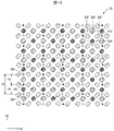
- FIG. 2 is a diagram showing a schematic configuration of a portion A of the display area DA of the display device 1 of Embodiment 1 shown in FIG.
- the display area DA of the display device 1 is provided with a plurality of pixels PIX, and each pixel PIX includes a red sub-pixel RSP, a green sub-pixel GSP, and a blue sub-pixel BSP. including.
- each pixel PIX includes a red sub-pixel RSP, a green sub-pixel GSP, and a blue sub-pixel BSP.
- a case where one pixel PIX is composed of one red sub-pixel RSP, two green sub-pixels GSP, and one blue sub-pixel BSP will be described as an example. not limited.
- one pixel PIX may be composed of one red sub-pixel RSP, one green sub-pixel GSP, and one blue sub-pixel BSP.
- subpixels of other colors may also be included.
- Pentile Diamond Pentile
- a case of having a Pentile (Diamond Pentile) pixel array will be described as an example, but the pixel array is not limited to this as in Embodiments 3 to 6 described later.
- FIG. 3A and 3B are diagrams showing the first spacer 30H and the second spacer 30L provided in the display device 1 of Embodiment 1.
- FIG. 3A and 3B are diagrams showing the first spacer 30H and the second spacer 30L provided in the display device 1 of Embodiment 1.
- FIG. 4 is a cross-sectional view of the display area DA of the display device 1 of Embodiment 1 shown in FIG. 2 taken along line B-B'.
- a barrier layer 3 As shown in FIG. 4, in the display area DA of the display device 1, a barrier layer 3, a thin film transistor layer 4 including a transistor TR, a red light emitting element 5R, a green light emitting element 5G, and a blue light emitting element 5B are formed on a substrate 12. , an edge cover layer 23, a first spacer 30H and a second spacer 30L (described later and shown in FIG. 3), a sealing layer 6, and a functional film 39 are provided in this order from the substrate 12 side.
- the red sub-pixels RSP provided in the display area DA of the display device 1 include red light-emitting elements 5R (first light-emitting elements), and the green sub-pixels GSP provided in the display area DA of the display device 1 include green light-emitting elements 5G (
- the blue sub-pixel BSP provided in the display area DA of the display device 1 includes the blue light emitting element 5B (third light emitting element).
- a red light emitting element 5R included in the red subpixel RSP includes a first electrode 22 (anode), a functional layer 24R including a red light emitting layer, and a second electrode 25 (cathode), and is included in the green subpixel GSP.
- the green light emitting element 5G includes a first electrode 22 (anode), a functional layer 24G including a green light emitting layer, and a second electrode 25 (cathode). It includes one electrode 22 (anode), a functional layer 24B including a blue light-emitting layer, and a second electrode 25 (cathode).
- the substrate 12 shown in FIG. 4 may be, for example, a resin substrate made of a resin material such as polyimide, or may be a glass substrate.
- a resin substrate made of a resin material such as polyimide is used as the substrate 12 will be described as an example, but the present invention is limited to this. never.
- a glass substrate can be used as the substrate 12 when the display device 1 is a non-flexible display device.
- the barrier layer 3 shown in FIG. 4 is a layer that prevents foreign substances such as water and oxygen from entering the transistor TR, the red light emitting element 5R, the green light emitting element 5G, and the blue light emitting element 5B.
- a silicon oxide film, a silicon nitride film, a silicon oxynitride film, or a laminate of these films can be used.
- the semiconductor films SEM, SEM', and SEM'' may be composed of, for example, low-temperature polysilicon (LTPS) or an oxide semiconductor (for example, an In--Ga--Zn--O based semiconductor).
- LTPS low-temperature polysilicon
- oxide semiconductor for example, an In--Ga--Zn--O based semiconductor.
- the transistor TR may have a bottom-gate structure.
- the gate electrode G, the source electrode S, and the drain electrode D can be composed of, for example, a single-layer or laminated film of metal containing at least one of aluminum, tungsten, molybdenum, tantalum, chromium, titanium, and copper.
- the inorganic insulating film 16, the inorganic insulating film 18, and the inorganic insulating film 20 can be composed of, for example, a silicon oxide film, a silicon nitride film, a silicon oxynitride film, or a laminated film thereof formed by the CVD method.
- the planarizing film 21 can be made of a coatable organic material such as polyimide or acryl.
- the red light emitting element 5R includes a first electrode 22 (anode) above the planarizing film 21, a functional layer 24R including a red light emitting layer, and a second electrode 25 (cathode).
- the blue light emitting element 5B includes a first electrode 22 (anode) above the planarizing film 21, a functional layer 24G including a green light emitting layer, and a second electrode 25 (cathode). It includes an upper first electrode 22 (anode), a functional layer 24B including a blue light-emitting layer, and a second electrode 25 (cathode).
- the insulating edge cover layer 23 covering the edge of the first electrode 22 (anode) can be formed, for example, by applying an organic material such as polyimide or acrylic and then patterning it by photolithography.
- the functional layer 24R including a red light-emitting layer is configured, for example, by laminating a hole injection layer, a hole transport layer, a red light-emitting layer, an electron transport layer, and an electron injection layer in this order from the first electrode 22 (anode) side. can do.
- the functional layers 24R including the red light emitting layer one or more layers other than the red light emitting layer may be omitted as appropriate.
- the functional layer 24G including a green light-emitting layer is configured by stacking, for example, a hole injection layer, a hole transport layer, a green light-emitting layer, an electron transport layer, and an electron injection layer in this order from the first electrode 22 (anode) side. can do.
- a hole injection layer for example, a hole injection layer, a hole transport layer, a green light-emitting layer, an electron transport layer, and an electron injection layer in this order from the first electrode 22 (anode) side.
- the functional layers 24G including the green light emitting layer one or more layers other than the green light emitting layer may be omitted as appropriate.
- the functional layer 24B including a blue light-emitting layer is configured, for example, by laminating a hole injection layer, a hole transport layer, a blue light-emitting layer, an electron transport layer, and an electron injection layer in this order from the first electrode 22 (anode) side. can do.
- the functional layers 24B including the blue light emitting layer one or more layers other than the blue light emitting layer may be omitted as appropriate.
- each of the functional layer 24R including the red light-emitting layer, the functional layer 24G including the green light-emitting layer, and the functional layer 24B including the blue light-emitting layer is formed by the same process using the same material.
- a hole injection layer, a hole transport layer formed in the same process using the same material, an electron transport layer formed in the same process using the same material, and electrons formed in the same process using the same material An injection layer will be described as an example, but the present invention is not limited to this.
- the hole injection layers included in the functional layers 24R, 24G, and 24B may be made of different materials.
- the included hole injection layers may be formed in the same process using the same material, and only the hole injection layer included in the remaining one functional layer may be formed in a separate process using a different material.
- the hole transport layers included in the functional layers 24R, 24G, and 24B may be formed of different materials.
- the hole transport layers included in each may be formed in the same process using the same material, and only the hole transport layer included in the remaining one functional layer may be formed in a separate process using a different material.
- each electron transport layer included in each of the functional layers 24R, 24G, and 24B may be formed of different materials. may be formed in the same process using the same material, and only the electron transport layer contained in the remaining one functional layer may be formed in a separate process using a different material.
- each electron injection layer included in each of the functional layers 24R, 24G, and 24B may be formed of different materials. may be formed in the same step using the same material, and only the electron injection layer included in the remaining one functional layer may be formed in a separate step using a different material.
- the red light emitting element 5R, the green light emitting element 5G, and the blue light emitting element 5B are described as an example in which they are OLEDs (organic light emitting diodes).
- the light emitting element 5R, the green light emitting element 5G and the blue light emitting element 5B may be QLEDs (quantum dot light emitting diodes).
- the remaining part of the red light emitting element 5R, the green light emitting element 5G and the blue light emitting element 5B may be QLEDs.
- the red light-emitting element 5R, the green light-emitting element 5G, and the blue light-emitting element 5B are OLEDs
- the light-emitting layers included in the respective color light-emitting elements are, for example, organic light-emitting layers formed by vapor deposition.
- the red light-emitting element 5R, the green light-emitting element 5G, and the blue light-emitting element 5B are QLEDs
- the light-emitting layers included in the light-emitting elements of each color are, for example, quantum dots formed by a coating method or an inkjet method.
- a control circuit including a transistor TR for controlling each of the red light emitting element 5R, the green light emitting element 5G and the blue light emitting element 5B includes a thin film transistor layer 4 including a transistor TR for each of the red sub-pixel RSP, the green sub-pixel GSP and the blue sub-pixel BSP. is provided in A control circuit including a transistor TR provided for each of the red sub-pixel RSP, the green sub-pixel GSP, and the blue sub-pixel BSP and the light emitting element are also collectively referred to as a sub-pixel circuit.
- the red light emitting element 5R, the green light emitting element 5G and the blue light emitting element 5B shown in FIG. 4 may be of top emission type or bottom emission type.
- the red light emitting element 5R, the green light emitting element 5G, and the blue light emitting element 5B are composed of, from the substrate 12 side, a first electrode 22 (anode), functional layers 24R, 24G, and 24B, and a second electrode 25 (cathode). Since it has a stacked structure formed in order, the second electrode 25 (cathode) is arranged as an upper layer than the first electrode 22 (anode). is made of an electrode material that reflects visible light, and the second electrode 25 (cathode) is made of an electrode material that transmits visible light.
- the second electrode 25 may be formed of an electrode material that transmits visible light
- the second electrode 25 may be formed of an electrode material that reflects visible light
- the red light emitting element 5R, the green light emitting element 5G, and the blue light emitting element 5B are composed of, from the substrate 12 side, the first electrode 22 (cathode), the functional layers 24R, 24G, and 24B, and the second electrode 25 (anode).
- the second electrode 25 (anode) is arranged as an upper layer than the first electrode 22 (cathode).
- 22 (cathode) is made of an electrode material that reflects visible light
- the second electrode 25 (anode) is made of an electrode material that transmits visible light.
- the (anode) may be formed from an electrode material that reflects visible light
- the first electrode 22 (cathode) may be formed from an electrode material that transmits visible light.
- the electrode material that reflects visible light is not particularly limited as long as it can reflect visible light and has electrical conductivity. , a laminate of the metal material and a transparent metal oxide (e.g., indium tin oxide, indium zinc oxide, indium gallium zinc oxide, etc.), or a laminate of the alloy and the transparent metal oxide. .
- a transparent metal oxide e.g., indium tin oxide, indium zinc oxide, indium gallium zinc oxide, etc.
- the electrode material that transmits visible light is not particularly limited as long as it can transmit visible light and has electrical conductivity. zinc oxide, etc.) or thin films made of metal materials such as Al, Mg, Li and Ag.
- the first electrode 22 and the second electrode 25 As a film formation method for the first electrode 22 and the second electrode 25, a general electrode formation method can be used. A vapor deposition (PVD) method, a chemical vapor deposition (CVD) method, or the like can be mentioned. Moreover, the patterning method of the first electrode 22 and the second electrode 25 is not particularly limited as long as it is a method capable of forming a desired pattern with high accuracy. law and so on.
- the sealing layer 6 shown in FIG. 4 is a translucent film. It can be composed of an inorganic sealing film 28 as an upper layer.
- the sealing layer 6 prevents foreign substances such as water and oxygen from penetrating into the red light emitting element 5R, the green light emitting element 5G and the blue light emitting element 5B.
- Each of the inorganic sealing film 26 and the inorganic sealing film 28 is an inorganic film, and may be composed of, for example, a silicon oxide film, a silicon nitride film, a silicon oxynitride film, or a laminated film thereof formed by a CVD method. can be done.
- the organic film 27 is a light-transmitting organic film having a flattening effect, and can be made of a coatable organic material such as acryl.
- the organic film 27 may be formed by an inkjet method, for example.
- the sealing layer 6 is formed of two layers of inorganic films and one layer of organic film provided between the two layers of inorganic films has been described as an example.
- the sealing layer 6 may be composed of only an inorganic film, may be composed of only an organic film, may be composed of one layer of inorganic film and two layers of organic film, or may be composed of two or more layers. may be composed of an inorganic film and two or more layers of organic films.
- the functional film 39 shown in FIG. 4 is, for example, a film having at least one of optical compensation function, touch sensor function, and protection function.
- the first spacers 30H and the second spacers 30L provided in the display area DA of the display device 1 will be described below with reference to FIGS.
- the red light emitting element 5R (the portion where the first electrode 22, the functional layer 24R and the second electrode 25 overlap), the green light emitting element 5G (the portion where the first electrode 22, the functional layer 24G, and the second electrode 25 overlap) and the blue light emitting element 5B (the portion where the first electrode 22, the functional layer 24B, and the second electrode 25 overlap) are provided.
- a plurality of first spacers 30H having the same height are provided at a constant first pitch P1 along the first direction D1, which is the left-right direction in FIG.
- second spacers 30L having a height lower than that of the spacers 30H are provided.
- n is 4, and the height between two first spacers 30H adjacent in the first direction D1, which is the horizontal direction in FIG. 2, is lower than the height of the first spacers 30H.
- three second spacers 30L are provided will be described as an example, but the present invention is not limited to this.
- one second spacer 30L having a height lower than the height of the first spacers 30H is provided between two first spacers 30H adjacent in the first direction D1, which is the horizontal direction in FIG. may
- the pitch of all the spacers including the first spacers 30H and the second spacers 30L in the first direction D1, which is the horizontal direction in the figure, is the first pitch.
- a constant second pitch P2 is obtained by dividing P1 into n equal parts.
- n ⁇ 1 (n is a natural number equal to or greater than 2) second spacers 30L having a height lower than that of the first spacers 30H are provided. Therefore, even if automatic optical inspection (AOI) is performed at a second pitch P2 that is 1/n of the first pitch P1 in the first direction D1, which is the horizontal direction in FIG. A defect is not detected at the location where the second spacer 30L is provided. This is because the results of automated optical inspection (AOI) at both the location where the first spacer 30H is provided and the location where the second spacer 30L having a height lower than the height of the first spacer 30H is , is detected as normal.
- the height LL of the second spacers 30L provided on the edge cover layer 23 is equal to the height LL of the first spacers provided on the edge cover layer 23. Since the height of 30H is lower than HH, only the first spacers 30H are in direct contact with the vapor deposition mask, and the second spacers 30L are not in direct contact with the vapor deposition mask. Therefore, in the case of the display device 1, the second spacer 30L is provided between two first spacers 30H adjacent in the first direction D1, which is the horizontal direction in FIG. can be performed more precisely, the possibility of transfer of foreign matter (transfer of vapor deposition material) due to contact with the vapor deposition mask does not increase.
- the red light emitting layer, the green light emitting layer, and the blue light emitting layer can be formed by a vapor deposition method using a vapor deposition mask that is a fine metal mask.
- the display device 1 includes, as spacers, a plurality of first spacers 30H having the same height and second spacers 30L having a height lower than that of the first spacers 30H. Therefore, the deposition mask contacts the higher first spacers 30H, but does not contact the lower second spacers 30L. Therefore, it is possible to reduce the contact area between the deposition mask and the spacers, thereby suppressing the transfer of foreign substances, such as deposition materials, formed on the second spacers 30L to the deposition mask.
- an automatic optical inspection that detects defects and the like without reducing the yield of the display device 1 due to transfer of foreign matter (transfer of vapor deposition material) due to contact with the vapor deposition mask. (AOI) can be performed more precisely.
- the second pitch P2 is set to 175 ⁇ m or less so that the inspection pitch of automatic optical inspection (AOI) can be set to 175 ⁇ m or less, but the present invention is not limited to this. never
- 23 has been described as an example, but the present invention is not limited to this.
- the first spacer 30H and the second spacer 30L may be provided in areas other than the areas where the red light emitting element 5R, the green light emitting element 5G and the blue light emitting element 5B are provided. For example, it may be provided between adjacent first electrodes.
- the first spacer 30H and the second spacer 30L may be formed in different steps using different materials, or may be formed in the same step or different steps using the same material. In this embodiment, the case where the first spacer 30H and the second spacer 30L are made of the same material will be described, but the present invention is not limited to this.
- the material for forming the first spacers 30H and the second spacers 30L for example, the material for forming the edge cover layer 23 may be used. can be formed by In this embodiment, the edge cover layer 23 is made of a photosensitive polyimide material, and the first spacers 30H and the second spacers 30L are made of a photosensitive acrylic material, but the present invention is not limited to this.
- the first spacers 30H and the second spacers 30L are formed of the same material as in the present embodiment, the first spacers 30H and the second spacers 30L can be formed in the same process, and the first spacers 30H and the second spacers 30L can be formed in the same process. Since the transmittance characteristics for each film thickness of the second spacer 30L are also the same, it becomes easy to design the film thickness of the first spacer 30H and the film thickness of the second spacer 30L.
- first spacers 30H, the second spacers 30L, and the edge cover layer 23 may be made of the same material.
- the first spacers 30H, the second spacers 30L and the edge cover layer 23 can be made of photosensitive polyimide material or photosensitive acrylic material.
- the first spacers 30H, the second spacers 30L, and the edge cover layer 23 are formed of the same material, the first spacers 30H, the second spacers 30L, and the edge cover layer 23 can be formed in the same process, and the first spacers 30H, the second spacers 30L, and the edge cover layer 23 have the same transmittance characteristics for each thickness, so that the thicknesses of the first spacers 30H, the second spacers 30L, and the edge cover layer 23 can be easily designed.
- the first spacers 30H and the second spacers 30L are preferably provided in the frame area NDA provided around the display area DA shown in FIG. 1 as well as the display area DA shown in FIG. That is, even in the frame area NDA of the display device 1, the pitch of all the spacers including the first spacers 30H and the second spacers 30L in the first direction D1, which is the horizontal direction in FIG. It is preferable to divide the first pitch P1 between the spacers 30H into n equal parts to obtain a constant second pitch P2. With such a configuration, not only the fine metal mask but also the common metal mask can be arranged at a predetermined height from the substrate.
- the frame area NDA as well as in the display area DA, automatic optical detection of defects can be performed without lowering the yield of the display device 1 due to transfer of foreign matter (transfer of vapor deposition material) due to contact with the vapor deposition mask.
- Formula checking can be done more precisely.
- the first spacers 30H and the second spacers 30L are also provided in the frame area NDA provided around the display area DA shown in FIG. 1 and the display area DA shown in FIG. are similarly provided.
- a sealing layer 6 including an organic film 27 is provided on the display area DA of the display device 1 .
- the organic film 27 included in the sealing layer 6 can be formed by coating using, for example, an inkjet method. Since the second spacers 30L having a lower height are provided, when the organic film 27 is applied using the inkjet method, the organic film 27 tends to spread through the second spacers 30L having a lower height. , the coatability of the organic film 27 can be improved.
- FIG. 5 is a diagram for explaining the manufacturing process of the display device 1 of Embodiment 1.
- FIG. 5 is a diagram for explaining the manufacturing process of the display device 1 of Embodiment 1.
- the manufacturing process of the display device 1 of Embodiment 1 includes a step of forming a barrier layer 3 and a thin film transistor layer 4 on a substrate (12) (step S1), and forming a first thin film transistor layer 4 on the thin film transistor layer 4.
- step S5 a step of forming a functional layer 24R including a red light-emitting layer, a functional layer 24G including a green light-emitting layer, and a functional layer 24B including a blue light-emitting layer (step S5); It includes a step of forming (step S6), a step of forming sealing layer 6 (step S7), and a step of forming functional film 39 (step S8).
- the first electrodes 22 are provided as described above with reference to FIGS.
- the spacers 30H and 30L are formed so that the pitch in the direction D1 is a constant second pitch P2 obtained by dividing the first pitch P1 into n equal parts.
- an insulating edge cover layer 23 covering the edges of the first electrodes 22 can be formed before forming the spacers 30H and 30L or during forming the spacers 30H and 30L. In this embodiment, the edge cover layer 23 is formed before the spacers 30H and 30L are formed, and the first spacers 30H and the second spacers 30L are formed on the edge cover layer 23 .
- the inspection pitch can be the second pitch P2.
- the step of optical inspection includes the step of forming the edge cover layer 23, the first spacers 30H and the second spacers 30L (step S3), the functional layer 24R including the red light emitting layer, and the green light emitting layer. and the step of forming the functional layer 24G including the blue light emitting layer (step S5).
- step S5 In the step of forming the functional layer 24R including the red light-emitting layer, the functional layer 24G including the green light-emitting layer, and the functional layer 24B including the blue light-emitting layer (step S5), at least the red light-emitting layer, the green light-emitting layer, and the blue light-emitting layer are formed.
- three different vapor deposition masks which are fine metal masks, are used.
- a vapor deposition mask for forming the red light emitting layer which is a fine metal mask, is arranged so as to be in contact with the first spacer 30H, and the red light is emitted through the vapor deposition mask for forming the red light emitting layer.
- a red light emitting layer is deposited on a portion corresponding to the sub-pixel RSP.
- a vapor deposition mask for forming the green light emitting layer which is a fine metal mask, is arranged so as to be in contact with the first spacer 30H, and the green light is emitted through the vapor deposition mask for forming the green light emitting layer.
- a green light emitting layer is deposited on a portion corresponding to the sub-pixel GSP.
- a vapor deposition mask for forming the blue light emitting layer which is a fine metal mask, is arranged so as to be in contact with the first spacer 30H, and blue light is emitted through the vapor deposition mask for forming the blue light emitting layer.
- a blue light emitting layer is deposited on a portion corresponding to the sub-pixel BSP.
- the red light emitting layer, the green light emitting layer, and the blue light emitting layer are formed.
- At least one of a fine metal mask and a common metal mask is used as necessary in the steps of forming the hole injection layer, the hole transport layer, the electron transport layer and the electron injection layer other than the step of forming the .
- step S6 a vapor deposition mask for forming the second electrode, which is a common metal mask, is used.
- the fine metal mask is arranged so as to be in contact with the first spacer 30H.
- the first spacers 30H and the second spacers 30H and 2nd spacers are also formed in the frame area NDA provided around the display area DA.
- 30L are provided in the same manner as the display area DA, the common metal mask is arranged so as to be in contact with the first spacers 30H in the frame area NDA.
- the sealing layer 6 including the organic film 27 is provided on the display area DA of the display device 1 .
- the organic film 27 included in the sealing layer 6 can be formed by, for example, an inkjet method.
- the first spacers 30H and the second spacers 30L lower in height than the first spacers 30H are provided in the display area DA, so the organic film 27 is applied using the inkjet method.
- the organic film 27 can easily spread through the second spacers 30L having a low height, so that the coatability of the organic film 27 can be improved.
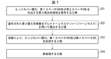
- FIG. 6 is a diagram showing an example of the process of forming the edge cover layer 23, the first spacers 30H and the second spacers 30L in the manufacturing process of the display device 1 of Embodiment 1 shown in FIG.
- a photosensitive polyimide material can be used as the first photosensitive resin.
- the applied photosensitive polyimide material is patterned into a predetermined shape by exposing and developing. can be done.
- a photosensitive acrylic material can be used as the second photosensitive resin.
- step S14 the step of exposing the coated second photosensitive resin using a gray-tone mask (halftone mask) (step S14), and the step of forming the first spacers 30H and the second spacers 30L by development (step S15). ) and the heat treatment step (step S16), the first spacers 30H and the second spacers 30L made of a material different from that of the edge cover layer 23 are placed at predetermined positions, in this embodiment, the edge cover layer 23 It can be formed on top with a predetermined height.
- a gray-tone mask halftone mask
- the edge cover layer 23 and the first spacers 30H and the second spacers 30L are formed in different steps using different materials.
- the first spacer 30H and the second spacer 30L are formed of the same material in the same step.
- FIG. 7 is a diagram showing another example of the process of forming the edge cover layer 23, the first spacers 30H and the second spacers 30L in the manufacturing process of the display device 1 of Embodiment 1 shown in FIG.
- the third photosensitive resin may be a photosensitive resin.
- a flexible polyimide material or a photosensitive acrylic material can be used.
- the edge cover layer 23, the first spacers 30H and the second spacers 30L are formed by a step of exposing the applied third photosensitive resin using a gray-tone mask (half-tone mask) (step S22) and development.
- the first spacers 30H and the second spacers 30L made of the same material as the edge cover layer 23 are placed at predetermined positions, in this embodiment, It can be formed with a predetermined height on the edge cover layer 23 . Note that the edge cover layer 23 and the first spacers 30H and the second spacers 30L are simultaneously formed in the same process.
- FIG. 8 A preferable value of (height of the second spacer 30L/height of the first spacer 30H) will be described below based on FIGS. 8, 9, 10 and 11.
- FIG. 8 A preferable value of (height of the second spacer 30L/height of the first spacer 30H) will be described below based on FIGS. 8, 9, 10 and 11.
- FIG. 8 is a diagram showing a schematic configuration of a display area DA of a display device 100 as a comparative example having only first spacers 30H.
- a plurality of first pitches P1 having the same height along the first direction D1, which is the horizontal direction in FIG. A spacer 30H is provided. Therefore, when automatic optical inspection (AOI) is performed at a pitch shorter than the first pitch P1 along the first direction D1, a defect is detected in the inspection of the portion where the first spacer 30H is not provided. Therefore, automatic optical inspection (AOI) cannot be performed at pitches shorter than the first pitch P1 along the first direction D1.
- FIG. 9 is a diagram showing a schematic configuration of the display area DA of a display device 200 as another comparative example that includes only the first spacers 30H.
- a plurality of first pitches P1 having the same height along the first direction D1, which is the left-right direction in FIG. A spacer 30H is provided. Therefore, automated optical inspection (AOI) can be performed at a relatively short first pitch P1 along the first direction D1.
- a plurality of first spacers 30H having the same height are provided at a constant third pitch P3 along the second direction D2, which is the vertical direction in FIG. It is Therefore, automated optical inspection (AOI) can be performed at a relatively short third pitch P3 along the second direction D2.
- all of the plurality of first spacers 30H having the same height are in contact with the vapor deposition mask. lowers the
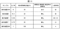
- FIG. 10 shows the relationship between the value of (the height LL of the second spacer 30L/the height HH of the first spacer 30H) and the relative foreign matter transfer amount in the display devices 1, 1', and 1'' of the first embodiment. It is a figure which shows.
- FIG. 11 shows the display device 100 shown in FIG. 8 as a comparative example including only the first spacers 30H, the display device 200 shown in FIG. 9 as another comparative example including only the first spacers 30H, and the second Relative foreign matter transfer amount and high sensitivity in the display devices 1, 1', and 1'' of Embodiment 1 where the spacer height/first spacer height values are 0.2, 0.45, and 0.75
- FIG. 5 is a diagram showing the presence or absence of erroneous detection at the time of inspection and characteristics related to inkjet applicability.
- IJ coatability inkjet coatability
- ⁇ in FIG. 11 indicates that the IJ coatability (inkjet coatability) is good
- x indicates poor IJ applicability (inkjet applicability).
- the first pitch P1 is relatively large, so the IJ coating property is very good.
- AOI automatic optical inspection
- the first pitch P1 is relatively small.
- the formula inspection (AOI) is performed, no erroneous detection occurs, but the IJ coating property is poor because only the tall first spacers 30H are formed at the relatively small first pitch P1.
- the display device 1 in which the value of (height LL of the second spacer 30L/height HH of the first spacer 30H) is 0.2, (height LL of the second spacer 30L/height of the first spacer 30H HH) is 0.45, and the display device 1'' is 0.75 (height LL of second spacer 30L/height HH of first spacer 30H). Also, even when automatic optical inspection (AOI) was performed at the second pitch P2 shorter than the first pitch P1, no erroneous detection occurred, and the IJ applicability was good.
- AOI automatic optical inspection
- the display device 1 in which the value of (height LL of the second spacer 30L/height HH of the first spacer 30H) is 0.2 is the best.
- the display device 1' having a value of (height LL/height HH of the first spacer 30H) of 0.45 has a value of (height LL of the second spacer 30L/height HH of the first spacer 30H) of 0.45. It is better than the display device 1'' which is 75.
- the value of (height LL of the second spacer 30L/height HH of the first spacer 30H) is preferably 0.2 or more and 0.75 or less.
- the spacers include a plurality of first spacers 30H having the same height and second spacers 30L having a height of 20% or more and 75% or less of the height HH of the first spacers 30H,
- the organic film 27 included in the sealing layer 6 is formed using an inkjet method, the coatability of the organic film 27 can be improved.
- n ⁇ 1 having a height lower than the height of the first spacers 30H (n is a natural number of 2 or more) is provided between two first spacers 30H adjacent in the second direction D2. ) second spacers 30L are provided, which is different from the first embodiment described above. Others are as described in the first embodiment. For convenience of explanation, members having the same functions as the members shown in the drawings of the first embodiment are denoted by the same reference numerals, and the explanation thereof is omitted.
- FIG. 12 is a diagram showing a schematic configuration of the display area DA of the display device 50 of the second embodiment.
- the red light emitting element 5R (the portion where the first electrode 22, the functional layer 24R, and the second electrode 25 overlap)
- the green light emitting element 5G the first electrode 22 and the functional layer 24G overlap with the second electrode 25
- the blue light emitting element 5B the area where the first electrode 22, the functional layer 24B and the second electrode 25 overlap.
- a plurality of first spacers 30H having the same height are provided at a constant first pitch P3 along the second direction D2, which is the 12 vertical direction.
- second spacers 30L having a height lower than that of the spacers 30H are provided.
- n is 2, and the height between two first spacers 30H adjacent in the second direction D2, which is the vertical direction in FIG. 12, is lower than the height of the first spacers 30H.
- the pitch of all the spacers including the first spacers 30H and the second spacers 30L in the second direction D2, which is the vertical direction in the figure, is the first pitch.
- a constant second pitch P4 is obtained by dividing P3 into n equal parts.
- n ⁇ 1 (n is a natural number equal to or greater than 2) second spacers 30L having a height lower than that of the first spacers 30H are provided. Therefore, even if automatic optical inspection (AOI) is performed at a second pitch P4 that is 1/n of the first pitch P3 in the second direction D2, which is the vertical direction in FIG. A defect is not detected at the location where the second spacer 30L is provided.
- a second spacer 30L is provided between two first spacers 30H adjacent in the second direction D2, which is the vertical direction in FIG.
- one pixel PIX is composed of one rectangular red sub-pixel RSP, one rectangular green sub-pixel GSP, and one rectangular blue sub-pixel BSP. It differs from the first and second embodiments described above in that the Others are as described in the first and second embodiments.
- members having the same functions as those shown in the drawings of Embodiments 1 and 2 are denoted by the same reference numerals, and their explanations are omitted.
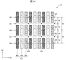
- FIG. 13 is a diagram showing a schematic configuration of the display area DA of the display device 51 of the third embodiment.
- the red light emitting element 5R (the portion where the first electrode 22, the functional layer 24R, and the second electrode 25 overlap), the green light emitting element 5G (the first electrode 22 and the functional layer 24G overlap with the second electrode 25) and the blue light emitting element 5B (the area where the first electrode 22, the functional layer 24B and the second electrode 25 overlap).
- a plurality of first spacers 30H having the same height are provided at a constant first pitch P1 along the first direction D1, which is the horizontal direction of 13. As shown in FIG.
- second spacers 30L having a height lower than that of the spacers 30H are provided.
- n is 3, and the height between two first spacers 30H adjacent in the first direction D1, which is the horizontal direction in FIG. 13, is lower than the height of the first spacers 30H.
- the pitch of all the spacers including the first spacers 30H and the second spacers 30L in the first direction D1, which is the horizontal direction in the figure, is the first pitch.
- a constant second pitch P2 is obtained by dividing P1 into n equal parts.
- n ⁇ 1 (n is a natural number equal to or greater than 2) second spacers 30L having a height lower than that of the first spacers 30H are provided. Therefore, even if automatic optical inspection (AOI) is performed at a second pitch P2 that is 1/n of the first pitch P1 in the first direction D1, which is the horizontal direction in FIG. A defect is not detected at the location where the second spacer 30L is provided.
- a second spacer 30L is provided between two first spacers 30H adjacent in the first direction D1, which is the horizontal direction in FIG.
- n ⁇ 1 (n is a natural number of 2 or more) having a height lower than the height of the first spacers 30H is provided between two first spacers 30H adjacent in the second direction D2. ) second spacers 30L are provided, which is different from the third embodiment described above. Others are as described in the third embodiment. For convenience of explanation, members having the same functions as the members shown in the drawings of the third embodiment are denoted by the same reference numerals, and the explanation thereof is omitted.
- FIG. 14 is a diagram showing a schematic configuration of the display area DA of the display device 52 of the fourth embodiment.
- the red light emitting element 5R (the portion where the first electrode 22, the functional layer 24R, and the second electrode 25 overlap), the green light emitting element 5G (the first electrode 22 and the functional layer 24G overlap with the second electrode 25) and the blue light emitting element 5B (the area where the first electrode 22, the functional layer 24B and the second electrode 25 overlap).
- a plurality of first spacers 30H having the same height are provided at a constant first pitch P3 along the second direction D2, which is the up-down direction of 14. As shown in FIG.
- second spacers 30L having a height lower than that of the spacers 30H are provided.
- n is 2, and the height between two first spacers 30H adjacent in the second direction D2, which is the vertical direction in FIG. 14, is lower than the height of the first spacers 30H.
- the pitch of all the spacers including the first spacers 30H and the second spacers 30L in the second direction D2, which is the vertical direction in the figure, is the first pitch.
- a constant second pitch P4 is obtained by dividing P3 into n equal parts.
- n ⁇ 1 (n is a natural number equal to or greater than 2) second spacers 30L having a height lower than that of the first spacers 30H are provided. Therefore, even if automatic optical inspection (AOI) is performed at a second pitch P4 that is 1/n of the first pitch P3 in the second direction D2, which is the vertical direction in FIG. A defect is not detected at the location where the second spacer 30L is provided.
- a second spacer 30L is provided between two first spacers 30H adjacent in the second direction D2, which is the vertical direction in FIG.
- an automatic optical inspection that detects defects and the like without reducing the yield of the display device 52 due to transfer of foreign matter (transfer of vapor deposition material) due to contact with the vapor deposition mask. (AOI) can be performed more precisely.
- one pixel PIX is composed of one red sub-pixel RSP, one green sub-pixel GSP, and one blue sub-pixel BSP.
- Others are as described in the first to fourth embodiments.
- members having the same functions as the members shown in the drawings of Embodiments 1 to 4 are denoted by the same reference numerals, and their explanations are omitted.
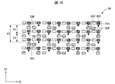
- FIG. 15 is a diagram showing a schematic configuration of the display area DA of the display device 53 of the fifth embodiment.
- the red light emitting element 5R (the portion where the first electrode 22, the functional layer 24R, and the second electrode 25 overlap), the green light emitting element 5G (the first electrode 22 and the functional layer 24G overlap with the second electrode 25) and the blue light emitting element 5B (the area where the first electrode 22, the functional layer 24B and the second electrode 25 overlap).
- a plurality of first spacers 30H having the same height are provided at a constant first pitch P1 along the first direction D1, which is the horizontal direction of 15. As shown in FIG.
- second spacers 30L having a height lower than that of the spacers 30H are provided.
- n is 4, and the height between two first spacers 30H adjacent in the first direction D1, which is the horizontal direction in FIG. 15, is lower than the height of the first spacers 30H.
- the pitch of all the spacers including the first spacers 30H and the second spacers 30L in the first direction D1, which is the horizontal direction in the figure, is the first pitch.
- a constant second pitch P2 is obtained by dividing P1 into n equal parts.
- n ⁇ 1 (n is a natural number equal to or greater than 2) second spacers 30L having a height lower than that of the first spacers 30H are provided. Therefore, even if automatic optical inspection (AOI) is performed at a second pitch P2 that is 1/n of the first pitch P1 in the first direction D1, which is the horizontal direction in FIG. A defect is not detected at the location where the second spacer 30L is provided.
- a second spacer 30L is provided between two first spacers 30H adjacent in the first direction D1, which is the horizontal direction in FIG.
- n ⁇ 1 (n is a natural number of 2 or more) having a height lower than the height of the first spacers 30H is provided between two first spacers 30H adjacent in the second direction D2. ) second spacers 30L are provided, which is different from the fifth embodiment described above. Others are as described in the fifth embodiment.
- members having the same functions as the members shown in the drawings of the fifth embodiment are denoted by the same reference numerals, and the explanation thereof is omitted.
- FIG. 16 is a diagram showing a schematic configuration of the display area DA of the display device 54 of the sixth embodiment.
- the red light emitting element 5R (the portion where the first electrode 22, the functional layer 24R, and the second electrode 25 overlap)
- the green light emitting element 5G the first electrode 22 and the functional layer 24G overlap with the second electrode 25
- the blue light emitting element 5B the area where the first electrode 22, the functional layer 24B and the second electrode 25 overlap.
- a plurality of first spacers 30H having the same height are provided at a constant first pitch P3 along the second direction D2, which is the 16 vertical direction.
- second spacers 30L having a height lower than that of the spacers 30H are provided.
- n is 2, and the height between two first spacers 30H adjacent in the second direction D2, which is the vertical direction in FIG. 16, is lower than the height of the first spacers 30H.
- the pitch of all the spacers including the first spacers 30H and the second spacers 30L in the second direction D2, which is the vertical direction in the figure, is the first pitch.
- a constant second pitch P4 is obtained by dividing P3 into n equal parts.
- n ⁇ 1 (n is a natural number equal to or greater than 2) second spacers 30L having a height lower than that of the first spacers 30H are provided. Therefore, even if automatic optical inspection (AOI) is performed at a second pitch P4 that is 1/n of the first pitch P3 in the second direction D2, which is the vertical direction in FIG. A defect is not detected at the location where the second spacer 30L is provided.
- a second spacer 30L is provided between two first spacers 30H adjacent in the second direction D2, which is the vertical direction in FIG.
- an automatic optical inspection that detects defects and the like without reducing the yield of the display device 54 due to transfer of foreign matter (transfer of vapor deposition material) due to contact with the vapor deposition mask. (AOI) can be performed more precisely.
- a substrate a thin film transistor layer provided on the substrate; a display region provided with a plurality of sub-pixels each including a light-emitting element having a first electrode, a functional layer including a light-emitting layer, and a second electrode in this order from the thin-film transistor layer side on the thin-film transistor layer; a plurality of first spacers provided at a constant first pitch along a constant direction and having the same height in areas other than the area where the light emitting elements are provided in the display area; n ⁇ 1 (n is 2 or more) provided in a region other than the region where the light emitting element is provided between the two first spacers adjacent in the certain direction and having a height lower than the height of the first spacers a natural number of) second spacers,
- the pitch in the given direction of all the spacers including the first spacer and the second spacer is a constant second pitch obtained by equally dividing the first pitch by n.
- the plurality of sub-pixels includes a first sub-pixel, a second sub-pixel, and a third sub-pixel; the first sub-pixel includes a first light-emitting element as the light-emitting element; the second sub-pixel includes a second light-emitting element as the light-emitting element; the third sub-pixel includes a third light-emitting element as the light-emitting element;
- the first light-emitting element includes a first light-emitting layer as the light-emitting layer,
- the second light-emitting element includes, as the light-emitting layer, a second light-emitting layer having an emission peak wavelength different from that of the first light-emitting layer,
- the third light-emitting element includes, as the light-emitting layer, a third light-emitting layer having an emission peak wavelength different from that of the first light-emitting layer and the second light-emitting layer, 7.
- the display device according to any one of modes 1 to 6, wherein
- n ⁇ 1 (n is a natural number of 2 or more) second spacers having a low height are formed, and the pitch of all the spacers including the first spacers and the second spacers in the predetermined direction is set to the first forming a spacer having a constant second pitch obtained by dividing the pitch of n equally;
- a step of forming a functional layer including the light-emitting layer by arranging a vapor deposition mask so as to be in contact with the first spacer and vapor-depositing the light-emitting layer in a predetermined shape through the vapor deposition mask; and forming a second electrode on the functional layer including the light-emitting layer.
- the first spacer and the second spacer are made of the same material, 12.
- forming the spacer further includes forming an edge cover layer covering an edge of the first electrode; the edge cover layer, the first spacer and the second spacer are made of the same material; 13.
- the present invention can be used for a display device and a method for manufacturing a display device.
Landscapes
- Physics & Mathematics (AREA)
- General Physics & Mathematics (AREA)
- Engineering & Computer Science (AREA)
- Theoretical Computer Science (AREA)
- Electroluminescent Light Sources (AREA)
Abstract
Description
基板と、
前記基板上に設けられた薄膜トランジスタ層と、
前記薄膜トランジスタ層上に、第1電極と、発光層を含む機能層と、第2電極とを、前記薄膜トランジスタ層側からこの順に備えた発光素子を含むサブ画素が複数個設けられた表示領域と、
前記表示領域において前記発光素子が設けられている領域以外に、一定方向に沿って一定の第1のピッチで設けられ、同一の高さを有する複数の第1スペーサと、
前記一定方向において隣接する2つの前記第1スペーサの間の前記発光素子が設けられている領域以外に設けられ、前記第1スペーサの高さよりも低い高さを有するn-1(nは2以上の自然数)個の第2スペーサと、を含み、
前記第1スペーサ及び前記第2スペーサを含む全てのスペーサの前記一定方向におけるピッチは、前記第1のピッチをn等分した一定の第2のピッチである。
基板上に薄膜トランジスタ層を形成する工程と、
前記薄膜トランジスタ層上に、第1電極を形成する工程と、
前記第1電極が設けられている領域以外を含む前記第1電極の端部より外側に、一定方向に沿って一定の第1のピッチで、同一の高さを有する複数の第1スペーサを形成するとともに、前記一定方向において隣接する2つの前記第1スペーサの間の前記第1電極が設けられている領域以外を含む前記第1電極の端部より外側に、前記第1スペーサの高さよりも低い高さを有するn-1(nは2以上の自然数)個の第2スペーサを形成し、前記第1スペーサ及び前記第2スペーサを含む全てのスペーサの前記一定方向におけるピッチを、前記第1のピッチをn等分した一定の第2のピッチとする、スペーサを形成する工程と、
前記第1スペーサと接するように、蒸着マスクを配置し、前記蒸着マスクを介して、所定形状に発光層を蒸着する、前記発光層を含む機能層を形成する工程と、
前記発光層を含む機能層上に第2電極を形成する工程と、を含む。
図1は、実施形態1の表示装置1の概略的な構成を示す平面図である。
次に、図12に基づき、本発明の実施形態2について説明する。本実施形態の表示装置50においては、第2方向D2において隣接する2つの第1スペーサ30Hの間に、第1スペーサ30Hの高さよりも低い高さを有するn-1(nは2以上の自然数)個の第2スペーサ30Lを設けている点において、上述した実施形態1とは異なる。その他については実施形態1において説明したとおりである。説明の便宜上、実施形態1の図面に示した部材と同じ機能を有する部材については、同じ符号を付し、その説明を省略する。
次に、図13に基づき、本発明の実施形態3について説明する。本実施形態の表示装置51においては、1画素PIXが、長方形である一つの赤色サブ画素RSPと、長方形である一つの緑色サブ画素GSPと、長方形である一つの青色サブ画素BSPとで構成されている点において、上述した実施形態1及び2とは異なる。その他については実施形態1及び2において説明したとおりである。説明の便宜上、実施形態1及び2の図面に示した部材と同じ機能を有する部材については、同じ符号を付し、その説明を省略する。
次に、図14に基づき、本発明の実施形態4について説明する。本実施形態の表示装置52においては、第2方向D2において隣接する2つの第1スペーサ30Hの間に、第1スペーサ30Hの高さよりも低い高さを有するn-1(nは2以上の自然数)個の第2スペーサ30Lを設けている点において、上述した実施形態3とは異なる。その他については実施形態3において説明したとおりである。説明の便宜上、実施形態3の図面に示した部材と同じ機能を有する部材については、同じ符号を付し、その説明を省略する。
次に、図15に基づき、本発明の実施形態5について説明する。本実施形態の表示装置53においては、1画素PIXが、一つの赤色サブ画素RSPと、一つの緑色サブ画素GSPと、一つの青色サブ画素BSPとで構成されているとともに、互いに隣接する2つの画素PIXのそれぞれにおいて青色サブ画素BSPの配置位置が異なる点において、上述した実施形態1から4とは異なる。その他については実施形態1から4において説明したとおりである。説明の便宜上、実施形態1から4の図面に示した部材と同じ機能を有する部材については、同じ符号を付し、その説明を省略する。
次に、図16に基づき、本発明の実施形態6について説明する。本実施形態の表示装置54においては、第2方向D2において隣接する2つの第1スペーサ30Hの間に、第1スペーサ30Hの高さよりも低い高さを有するn-1(nは2以上の自然数)個の第2スペーサ30Lを設けている点において、上述した実施形態5とは異なる。その他については実施形態5において説明したとおりである。説明の便宜上、実施形態5の図面に示した部材と同じ機能を有する部材については、同じ符号を付し、その説明を省略する。
〔態様1〕
基板と、
前記基板上に設けられた薄膜トランジスタ層と、
前記薄膜トランジスタ層上に、第1電極と、発光層を含む機能層と、第2電極とを、前記薄膜トランジスタ層側からこの順に備えた発光素子を含むサブ画素が複数個設けられた表示領域と、
前記表示領域において前記発光素子が設けられている領域以外に、一定方向に沿って一定の第1のピッチで設けられ、同一の高さを有する複数の第1スペーサと、
前記一定方向において隣接する2つの前記第1スペーサの間の前記発光素子が設けられている領域以外に設けられ、前記第1スペーサの高さよりも低い高さを有するn-1(nは2以上の自然数)個の第2スペーサと、を含み、
前記第1スペーサ及び前記第2スペーサを含む全てのスペーサの前記一定方向におけるピッチは、前記第1のピッチをn等分した一定の第2のピッチである、表示装置。
前記第1スペーサ及び前記第2スペーサは、同一材料で形成されている、態様1に記載の表示装置。
前記第1電極のエッジを覆うエッジカバー層をさらに備え、
前記第1スペーサ及び前記第2スペーサは、前記エッジカバー層上に設けられている、態様1または2に記載の表示装置。
前記エッジカバー層、前記第1スペーサ及び前記第2スペーサは、同一材料で形成されている、態様3に記載の表示装置。
前記第2のピッチは、175μm以下である、態様1から4の何れかに記載の表示装置。
前記第1スペーサ及び前記第2スペーサを含む全てのスペーサのうちの前記一定方向において隣接する2つのスペーサ間には、1つの前記サブ画素が配置されている、態様1から5の何れかに記載の表示装置。
前記複数個のサブ画素は、第1サブ画素と、第2サブ画素と、第3サブ画素とを含み、
前記第1サブ画素は、前記発光素子として、第1発光素子を含み、
前記第2サブ画素は、前記発光素子として、第2発光素子を含み、
前記第3サブ画素は、前記発光素子として、第3発光素子を含み、
前記第1発光素子は、前記発光層として、第1発光層を備え、
前記第2発光素子は、前記発光層として、前記第1発光層とは発光ピーク波長が異なる第2発光層を備え、
前記第3発光素子は、前記発光層として、前記第1発光層及び前記第2発光層とは発光ピーク波長が異なる第3発光層を備え、
前記第1発光層、前記第2発光層及び前記第3発光層の少なくとも一つは、有機材料からなる、態様1から6の何れかに記載の表示装置。
前記表示領域上には、有機膜を含む封止層が設けられている、態様1から7の何れかに記載の表示装置。
前記第2スペーサの高さ/前記第1スペーサの高さの値は、0.2以上、0.75以下である、態様1から8の何れかに記載の表示装置。
基板上に薄膜トランジスタ層を形成する工程と、
前記薄膜トランジスタ層上に、第1電極を形成する工程と、
前記第1電極が設けられている領域以外を含む前記第1電極の端部より外側に、一定方向に沿って一定の第1のピッチで、同一の高さを有する複数の第1スペーサを形成するとともに、前記一定方向において隣接する2つの前記第1スペーサの間の前記第1電極が設けられている領域以外を含む前記第1電極の端部より外側に、前記第1スペーサの高さよりも低い高さを有するn-1(nは2以上の自然数)個の第2スペーサを形成し、前記第1スペーサ及び前記第2スペーサを含む全てのスペーサの前記一定方向におけるピッチを、前記第1のピッチをn等分した一定の第2のピッチとする、スペーサを形成する工程と、
前記第1スペーサと接するように、蒸着マスクを配置し、前記蒸着マスクを介して、所定形状に発光層を蒸着する、前記発光層を含む機能層を形成する工程と、
前記発光層を含む機能層上に第2電極を形成する工程と、を含む、表示装置の製造方法。
前記スペーサを形成する工程と、前記発光層を含む機能層を形成する工程との間に、光学式検査を行う工程がさらに含まれ、
前記光学式検査を行う工程においては、検査ピッチは前記第2のピッチである、態様10に記載の表示装置の製造方法。
前記第1スペーサ及び前記第2スペーサは、同一材料で形成され、
前記スペーサを形成する工程においては、前記第1スペーサと前記第2スペーサとは、同一工程で形成される、態様10または11に記載の表示装置の製造方法。
前記スペーサを形成する工程の前に、前記第1電極のエッジを覆うエッジカバー層を形成する工程をさらに含み、
前記スペーサを形成する工程においては、前記第1スペーサ及び前記第2スペーサは、前記エッジカバー層上に設けられる、態様10から12の何れかに記載の表示装置の製造方法。
前記スペーサを形成する工程には、前記第1電極のエッジを覆うエッジカバー層を形成する工程がさらに含まれ、
前記エッジカバー層、前記第1スペーサ及び前記第2スペーサは、同一材料であり、
前記スペーサを形成する工程においては、前記エッジカバー層と、前記第1スペーサと、前記第2スペーサとは、同一工程で形成される、態様10から12の何れかに記載の表示装置の製造方法。
前記第2電極を形成する工程の後に、有機膜を含む封止層を形成する工程がさらに含まれ、
前記有機膜は、インクジェット法によって形成される、態様10から14の何れかに記載の表示装置の製造方法。
前記スペーサを形成する工程においては、前記第2スペーサの高さ/前記第1スペーサの高さの値が、0.2以上、0.75以下を満たすように、前記第1スペーサ及び前記第2スペーサを形成する、態様10から15の何れかに記載の表示装置の製造方法。
本発明は上述した各実施形態に限定されるものではなく、請求項に示した範囲で種々の変更が可能であり、異なる実施形態にそれぞれ開示された技術的手段を適宜組み合わせて得られる実施形態についても本発明の技術的範囲に含まれる。さらに、各実施形態にそれぞれ開示された技術的手段を組み合わせることにより、新しい技術的特徴を形成することができる。
3 バリア層
4 薄膜トランジスタ層
5R 赤色発光素子(第1発光素子)
5G 緑色発光素子(第2発光素子)
5B 青色発光素子(第3発光素子)
6 封止層
12 基板
16、18、20 無機絶縁膜
21 平坦化膜
22 第1電極
23 エッジカバー層
24R 赤色発光層(第1発光層)を含む機能層
24G 緑色発光層(第2発光層)を含む機能層
24B 青色発光層(第3発光層)を含む機能層
25 第2電極
26、28 無機封止膜
27 有機膜
30H 第1スペーサ
30L 第2スペーサ
39 機能フィルム
PIX 画素
RSP 赤色サブ画素(第1サブ画素)
GSP 緑色サブ画素(第2サブ画素)
BSP 青色サブ画素(第3サブ画素)
TR トランジスタ
SEM、SEM’、SEM’’ 半導体膜
G ゲート電極
D ドレイン電極
S ソース電極
DA 表示領域
NDA 額縁領域
D1 第1方向(一定方向)
D2 第2方向(一定方向)
P1、P3 第1のピッチ
P2、P4 第2のピッチ
Claims (16)
- 基板と、
前記基板上に設けられた薄膜トランジスタ層と、
前記薄膜トランジスタ層上に、第1電極と、発光層を含む機能層と、第2電極とを、前記薄膜トランジスタ層側からこの順に備えた発光素子を含むサブ画素が複数個設けられた表示領域と、
前記表示領域において前記発光素子が設けられている領域以外に、一定方向に沿って一定の第1のピッチで設けられ、同一の高さを有する複数の第1スペーサと、
前記一定方向において隣接する2つの前記第1スペーサの間の前記発光素子が設けられている領域以外に設けられ、前記第1スペーサの高さよりも低い高さを有するn-1(nは2以上の自然数)個の第2スペーサと、を含み、
前記第1スペーサ及び前記第2スペーサを含む全てのスペーサの前記一定方向におけるピッチは、前記第1のピッチをn等分した一定の第2のピッチである、表示装置。 - 前記第1スペーサ及び前記第2スペーサは、同一材料で形成されている、請求項1に記載の表示装置。
- 前記第1電極のエッジを覆うエッジカバー層をさらに備え、
前記第1スペーサ及び前記第2スペーサは、前記エッジカバー層上に設けられている、請求項1または2に記載の表示装置。 - 前記エッジカバー層、前記第1スペーサ及び前記第2スペーサは、同一材料で形成されている、請求項3に記載の表示装置。
- 前記第2のピッチは、175μm以下である、請求項1から4の何れか1項に記載の表示装置。
- 前記第1スペーサ及び前記第2スペーサを含む全てのスペーサのうちの前記一定方向において隣接する2つのスペーサ間には、1つの前記サブ画素が配置されている、請求項1から5の何れか1項に記載の表示装置。
- 前記複数個のサブ画素は、第1サブ画素と、第2サブ画素と、第3サブ画素とを含み、
前記第1サブ画素は、前記発光素子として、第1発光素子を含み、
前記第2サブ画素は、前記発光素子として、第2発光素子を含み、
前記第3サブ画素は、前記発光素子として、第3発光素子を含み、
前記第1発光素子は、前記発光層として、第1発光層を備え、
前記第2発光素子は、前記発光層として、前記第1発光層とは発光ピーク波長が異なる第2発光層を備え、
前記第3発光素子は、前記発光層として、前記第1発光層及び前記第2発光層とは発光ピーク波長が異なる第3発光層を備え、
前記第1発光層、前記第2発光層及び前記第3発光層の少なくとも一つは、有機材料からなる、請求項1から6の何れか1項に記載の表示装置。 - 前記表示領域上には、有機膜を含む封止層が設けられている、請求項1から7の何れか1項に記載の表示装置。
- 前記第2スペーサの高さ/前記第1スペーサの高さの値は、0.2以上、0.75以下である、請求項1から8の何れか1項に記載の表示装置。
- 基板上に薄膜トランジスタ層を形成する工程と、
前記薄膜トランジスタ層上に、第1電極を形成する工程と、
前記第1電極が設けられている領域以外を含む前記第1電極の端部より外側に、一定方向に沿って一定の第1のピッチで、同一の高さを有する複数の第1スペーサを形成するとともに、前記一定方向において隣接する2つの前記第1スペーサの間の前記第1電極が設けられている領域以外を含む前記第1電極の端部より外側に、前記第1スペーサの高さよりも低い高さを有するn-1(nは2以上の自然数)個の第2スペーサを形成し、前記第1スペーサ及び前記第2スペーサを含む全てのスペーサの前記一定方向におけるピッチを、前記第1のピッチをn等分した一定の第2のピッチとする、スペーサを形成する工程と、
前記第1スペーサと接するように、蒸着マスクを配置し、前記蒸着マスクを介して、所定形状に発光層を蒸着する、前記発光層を含む機能層を形成する工程と、
前記発光層を含む機能層上に第2電極を形成する工程と、を含む、表示装置の製造方法。 - 前記スペーサを形成する工程と、前記発光層を含む機能層を形成する工程との間に、光学式検査を行う工程がさらに含まれ、
前記光学式検査を行う工程においては、検査ピッチは前記第2のピッチである、請求項10に記載の表示装置の製造方法。 - 前記第1スペーサ及び前記第2スペーサは、同一材料で形成され、
前記スペーサを形成する工程においては、前記第1スペーサと前記第2スペーサとは、同一工程で形成される、請求項10または11に記載の表示装置の製造方法。 - 前記スペーサを形成する工程の前に、前記第1電極のエッジを覆うエッジカバー層を形成する工程をさらに含み、
前記スペーサを形成する工程においては、前記第1スペーサ及び前記第2スペーサは、前記エッジカバー層上に設けられる、請求項10から12の何れか1項に記載の表示装置の製造方法。 - 前記スペーサを形成する工程には、前記第1電極のエッジを覆うエッジカバー層を形成する工程がさらに含まれ、
前記エッジカバー層、前記第1スペーサ及び前記第2スペーサは、同一材料であり、
前記スペーサを形成する工程においては、前記エッジカバー層と、前記第1スペーサと、前記第2スペーサとは、同一工程で形成される、請求項10から12の何れか1項に記載の表示装置の製造方法。 - 前記第2電極を形成する工程の後に、有機膜を含む封止層を形成する工程がさらに含まれ、
前記有機膜は、インクジェット法によって形成される、請求項10から14の何れか1項に記載の表示装置の製造方法。 - 前記スペーサを形成する工程においては、前記第2スペーサの高さ/前記第1スペーサの高さの値が、0.2以上、0.75以下を満たすように、前記第1スペーサ及び前記第2スペーサを形成する、請求項10から15の何れか1項に記載の表示装置の製造方法。
Priority Applications (2)
| Application Number | Priority Date | Filing Date | Title |
|---|---|---|---|
| PCT/JP2021/016280 WO2022224398A1 (ja) | 2021-04-22 | 2021-04-22 | 表示装置及び表示装置の製造方法 |
| JP2023515969A JPWO2022224398A1 (ja) | 2021-04-22 | 2021-04-22 |
Applications Claiming Priority (1)
| Application Number | Priority Date | Filing Date | Title |
|---|---|---|---|
| PCT/JP2021/016280 WO2022224398A1 (ja) | 2021-04-22 | 2021-04-22 | 表示装置及び表示装置の製造方法 |
Publications (1)
| Publication Number | Publication Date |
|---|---|
| WO2022224398A1 true WO2022224398A1 (ja) | 2022-10-27 |
Family
ID=83722200
Family Applications (1)
| Application Number | Title | Priority Date | Filing Date |
|---|---|---|---|
| PCT/JP2021/016280 WO2022224398A1 (ja) | 2021-04-22 | 2021-04-22 | 表示装置及び表示装置の製造方法 |
Country Status (2)
| Country | Link |
|---|---|
| JP (1) | JPWO2022224398A1 (ja) |
| WO (1) | WO2022224398A1 (ja) |
Citations (8)
| Publication number | Priority date | Publication date | Assignee | Title |
|---|---|---|---|---|
| JP2010140852A (ja) * | 2008-12-15 | 2010-06-24 | Sharp Corp | 有機el表示装置及びその製造方法 |
| US20100291720A1 (en) * | 2009-05-12 | 2010-11-18 | Woochan Kim | Method of fabricating organic light emitting diode display |
| JP2011154797A (ja) * | 2010-01-26 | 2011-08-11 | Seiko Epson Corp | 有機el装置及び電子機器 |
| JP2013089475A (ja) * | 2011-10-19 | 2013-05-13 | Canon Inc | 発光表示装置及びその製造方法 |
| US20140027729A1 (en) * | 2012-07-27 | 2014-01-30 | Samsung Display Co., Ltd. | Organic light emitting diode display and manufacturing method thereof |
| JP2014220256A (ja) * | 2004-09-29 | 2014-11-20 | 株式会社半導体エネルギー研究所 | 半導体装置、表示モジュール及び電子機器 |
| JP2016018734A (ja) * | 2014-07-10 | 2016-02-01 | 株式会社ジャパンディスプレイ | 表示装置及びその製造方法 |
| JP2020080224A (ja) * | 2018-11-12 | 2020-05-28 | 株式会社ジャパンディスプレイ | 表示装置、及びその製造方法 |
-
2021
- 2021-04-22 JP JP2023515969A patent/JPWO2022224398A1/ja active Pending
- 2021-04-22 WO PCT/JP2021/016280 patent/WO2022224398A1/ja active Application Filing
Patent Citations (8)
| Publication number | Priority date | Publication date | Assignee | Title |
|---|---|---|---|---|
| JP2014220256A (ja) * | 2004-09-29 | 2014-11-20 | 株式会社半導体エネルギー研究所 | 半導体装置、表示モジュール及び電子機器 |
| JP2010140852A (ja) * | 2008-12-15 | 2010-06-24 | Sharp Corp | 有機el表示装置及びその製造方法 |
| US20100291720A1 (en) * | 2009-05-12 | 2010-11-18 | Woochan Kim | Method of fabricating organic light emitting diode display |
| JP2011154797A (ja) * | 2010-01-26 | 2011-08-11 | Seiko Epson Corp | 有機el装置及び電子機器 |
| JP2013089475A (ja) * | 2011-10-19 | 2013-05-13 | Canon Inc | 発光表示装置及びその製造方法 |
| US20140027729A1 (en) * | 2012-07-27 | 2014-01-30 | Samsung Display Co., Ltd. | Organic light emitting diode display and manufacturing method thereof |
| JP2016018734A (ja) * | 2014-07-10 | 2016-02-01 | 株式会社ジャパンディスプレイ | 表示装置及びその製造方法 |
| JP2020080224A (ja) * | 2018-11-12 | 2020-05-28 | 株式会社ジャパンディスプレイ | 表示装置、及びその製造方法 |
Also Published As
| Publication number | Publication date |
|---|---|
| JPWO2022224398A1 (ja) | 2022-10-27 |
Similar Documents
| Publication | Publication Date | Title |
|---|---|---|
| US8963137B2 (en) | Organic light-emitting display device and method of fabricating the same | |
| US8587194B2 (en) | Top emission type organic electroluminescent display device and method of fabricating the same | |
| KR102315094B1 (ko) | 고 개구율 유기발광 다이오드 표시장치 및 그 제조방법 | |
| KR101961190B1 (ko) | 유기전압 발광소자 및 이의 제조방법 | |
| KR101575168B1 (ko) | 상부발광 방식 유기전계 발광소자 및 이의 제조 방법 | |
| US8729538B2 (en) | Organic light emitting diode device and method for fabricating the same | |
| KR102016070B1 (ko) | 플렉서블 유기전계 발광소자 및 그의 제조방법 | |
| KR101890469B1 (ko) | 표시장치 및 그 제조 방법 | |
| JP6223070B2 (ja) | 有機el表示装置及び有機el表示装置の製造方法 | |
| JP5486920B2 (ja) | 有機el装置及びその製造方法 | |
| KR20090036523A (ko) | 표시장치 및 그 제조방법 | |
| US20220139970A1 (en) | Display apparatus and method of manufacturing the same | |
| WO2020065963A1 (ja) | 表示装置及び表示装置の製造方法 | |
| KR101622563B1 (ko) | 상부발광 방식 유기전계 발광소자 | |
| KR101950837B1 (ko) | 유기전계발광소자 및 그 제조방법 | |
| KR102355605B1 (ko) | 유기발광다이오드 표시장치 및 그 제조방법 | |
| WO2022224398A1 (ja) | 表示装置及び表示装置の製造方法 | |
| US20210408484A1 (en) | Electronic device | |
| US20200274097A1 (en) | Display device, exposure device, and manufacturing method of display device | |
| WO2022113333A1 (ja) | 表示装置 | |
| US20240164145A1 (en) | Display device and method for manufacturing display device | |
| US20230209972A1 (en) | Display device and display device manufacturing method | |
| KR100497094B1 (ko) | 하이브리드 구조 유기전계 발광소자 및 그의 제조방법 | |
| WO2022195679A1 (ja) | 表示装置、表示パネル及び表示装置の製造方法 | |
| WO2021260901A1 (ja) | 表示装置及びその製造方法 |
Legal Events
| Date | Code | Title | Description |
|---|---|---|---|
| 121 | Ep: the epo has been informed by wipo that ep was designated in this application |
Ref document number: 21937891 Country of ref document: EP Kind code of ref document: A1 |
|
| WWE | Wipo information: entry into national phase |
Ref document number: 2023515969 Country of ref document: JP |
|
| WWE | Wipo information: entry into national phase |
Ref document number: 18284185 Country of ref document: US |
|
| NENP | Non-entry into the national phase |
Ref country code: DE |
|
| 122 | Ep: pct application non-entry in european phase |
Ref document number: 21937891 Country of ref document: EP Kind code of ref document: A1 |