WO2022195679A1 - 表示装置、表示パネル及び表示装置の製造方法 - Google Patents
表示装置、表示パネル及び表示装置の製造方法 Download PDFInfo
- Publication number
- WO2022195679A1 WO2022195679A1 PCT/JP2021/010390 JP2021010390W WO2022195679A1 WO 2022195679 A1 WO2022195679 A1 WO 2022195679A1 JP 2021010390 W JP2021010390 W JP 2021010390W WO 2022195679 A1 WO2022195679 A1 WO 2022195679A1
- Authority
- WO
- WIPO (PCT)
- Prior art keywords
- display device
- size
- light emitting
- pixel
- contact surface
- Prior art date
Links
- 238000004519 manufacturing process Methods 0.000 title claims description 36
- 239000010410 layer Substances 0.000 claims abstract description 372
- 239000002346 layers by function Substances 0.000 claims abstract description 84
- 239000000758 substrate Substances 0.000 claims abstract description 60
- 238000007740 vapor deposition Methods 0.000 claims description 143
- 238000000034 method Methods 0.000 claims description 51
- 238000013459 approach Methods 0.000 claims description 24
- 239000010408 film Substances 0.000 description 65
- 238000002347 injection Methods 0.000 description 25
- 239000007924 injection Substances 0.000 description 25
- 239000000463 material Substances 0.000 description 24
- 230000005525 hole transport Effects 0.000 description 17
- 238000013461 design Methods 0.000 description 12
- 238000007789 sealing Methods 0.000 description 11
- 239000007772 electrode material Substances 0.000 description 10
- 238000010586 diagram Methods 0.000 description 9
- 239000011159 matrix material Substances 0.000 description 8
- 238000000151 deposition Methods 0.000 description 7
- 230000008021 deposition Effects 0.000 description 7
- 239000000203 mixture Substances 0.000 description 6
- 239000004065 semiconductor Substances 0.000 description 6
- 239000010409 thin film Substances 0.000 description 6
- 239000004642 Polyimide Substances 0.000 description 4
- XLOMVQKBTHCTTD-UHFFFAOYSA-N Zinc monoxide Chemical compound [Zn]=O XLOMVQKBTHCTTD-UHFFFAOYSA-N 0.000 description 4
- 238000005229 chemical vapour deposition Methods 0.000 description 4
- 238000006073 displacement reaction Methods 0.000 description 4
- 229920001721 polyimide Polymers 0.000 description 4
- 239000011347 resin Substances 0.000 description 4
- 229920005989 resin Polymers 0.000 description 4
- 229910001374 Invar Inorganic materials 0.000 description 3
- 229910052581 Si3N4 Inorganic materials 0.000 description 3
- XUIMIQQOPSSXEZ-UHFFFAOYSA-N Silicon Chemical compound [Si] XUIMIQQOPSSXEZ-UHFFFAOYSA-N 0.000 description 3
- 230000004888 barrier function Effects 0.000 description 3
- 239000011368 organic material Substances 0.000 description 3
- 229910052710 silicon Inorganic materials 0.000 description 3
- 239000010703 silicon Substances 0.000 description 3
- HQVNEWCFYHHQES-UHFFFAOYSA-N silicon nitride Chemical compound N12[Si]34N5[Si]62N3[Si]51N64 HQVNEWCFYHHQES-UHFFFAOYSA-N 0.000 description 3
- VYPSYNLAJGMNEJ-UHFFFAOYSA-N Silicium dioxide Chemical compound O=[Si]=O VYPSYNLAJGMNEJ-UHFFFAOYSA-N 0.000 description 2
- -1 acryl Chemical group 0.000 description 2
- 229910045601 alloy Inorganic materials 0.000 description 2
- 239000000956 alloy Substances 0.000 description 2
- 229910052782 aluminium Inorganic materials 0.000 description 2
- QVGXLLKOCUKJST-UHFFFAOYSA-N atomic oxygen Chemical compound [O] QVGXLLKOCUKJST-UHFFFAOYSA-N 0.000 description 2
- 230000015572 biosynthetic process Effects 0.000 description 2
- 239000011521 glass Substances 0.000 description 2
- 238000010030 laminating Methods 0.000 description 2
- 229910052751 metal Inorganic materials 0.000 description 2
- 239000002184 metal Substances 0.000 description 2
- 239000007769 metal material Substances 0.000 description 2
- 229910044991 metal oxide Inorganic materials 0.000 description 2
- 150000004706 metal oxides Chemical class 0.000 description 2
- 229910052760 oxygen Inorganic materials 0.000 description 2
- 239000001301 oxygen Substances 0.000 description 2
- 238000000059 patterning Methods 0.000 description 2
- 238000000206 photolithography Methods 0.000 description 2
- 238000005240 physical vapour deposition Methods 0.000 description 2
- 229910052814 silicon oxide Inorganic materials 0.000 description 2
- 239000000126 substance Substances 0.000 description 2
- XLYOFNOQVPJJNP-UHFFFAOYSA-N water Substances O XLYOFNOQVPJJNP-UHFFFAOYSA-N 0.000 description 2
- 239000011787 zinc oxide Substances 0.000 description 2
- VYZAMTAEIAYCRO-UHFFFAOYSA-N Chromium Chemical compound [Cr] VYZAMTAEIAYCRO-UHFFFAOYSA-N 0.000 description 1
- RYGMFSIKBFXOCR-UHFFFAOYSA-N Copper Chemical compound [Cu] RYGMFSIKBFXOCR-UHFFFAOYSA-N 0.000 description 1
- GYHNNYVSQQEPJS-UHFFFAOYSA-N Gallium Chemical compound [Ga] GYHNNYVSQQEPJS-UHFFFAOYSA-N 0.000 description 1
- ZOKXTWBITQBERF-UHFFFAOYSA-N Molybdenum Chemical compound [Mo] ZOKXTWBITQBERF-UHFFFAOYSA-N 0.000 description 1
- RTAQQCXQSZGOHL-UHFFFAOYSA-N Titanium Chemical compound [Ti] RTAQQCXQSZGOHL-UHFFFAOYSA-N 0.000 description 1
- NIXOWILDQLNWCW-UHFFFAOYSA-N acrylic acid group Chemical group C(C=C)(=O)O NIXOWILDQLNWCW-UHFFFAOYSA-N 0.000 description 1
- XAGFODPZIPBFFR-UHFFFAOYSA-N aluminium Chemical compound [Al] XAGFODPZIPBFFR-UHFFFAOYSA-N 0.000 description 1
- 229910052804 chromium Inorganic materials 0.000 description 1
- 239000011651 chromium Substances 0.000 description 1
- 238000000576 coating method Methods 0.000 description 1
- 239000003086 colorant Substances 0.000 description 1
- 238000004040 coloring Methods 0.000 description 1
- 229910052802 copper Inorganic materials 0.000 description 1
- 239000010949 copper Substances 0.000 description 1
- 238000005520 cutting process Methods 0.000 description 1
- 238000011161 development Methods 0.000 description 1
- 238000009826 distribution Methods 0.000 description 1
- 230000000694 effects Effects 0.000 description 1
- 238000005530 etching Methods 0.000 description 1
- 230000008020 evaporation Effects 0.000 description 1
- 238000001704 evaporation Methods 0.000 description 1
- 229910052733 gallium Inorganic materials 0.000 description 1
- 229910052738 indium Inorganic materials 0.000 description 1
- APFVFJFRJDLVQX-UHFFFAOYSA-N indium atom Chemical compound [In] APFVFJFRJDLVQX-UHFFFAOYSA-N 0.000 description 1
- AMGQUBHHOARCQH-UHFFFAOYSA-N indium;oxotin Chemical compound [In].[Sn]=O AMGQUBHHOARCQH-UHFFFAOYSA-N 0.000 description 1
- 238000003475 lamination Methods 0.000 description 1
- 229910052744 lithium Inorganic materials 0.000 description 1
- 229910052749 magnesium Inorganic materials 0.000 description 1
- 238000005259 measurement Methods 0.000 description 1
- 229910052750 molybdenum Inorganic materials 0.000 description 1
- 239000011733 molybdenum Substances 0.000 description 1
- 230000003287 optical effect Effects 0.000 description 1
- 230000000149 penetrating effect Effects 0.000 description 1
- 229910021420 polycrystalline silicon Inorganic materials 0.000 description 1
- 229920005591 polysilicon Polymers 0.000 description 1
- 238000011160 research Methods 0.000 description 1
- 229910052709 silver Inorganic materials 0.000 description 1
- 239000002356 single layer Substances 0.000 description 1
- 238000004513 sizing Methods 0.000 description 1
- 229910052715 tantalum Inorganic materials 0.000 description 1
- GUVRBAGPIYLISA-UHFFFAOYSA-N tantalum atom Chemical compound [Ta] GUVRBAGPIYLISA-UHFFFAOYSA-N 0.000 description 1
- 229910052719 titanium Inorganic materials 0.000 description 1
- 239000010936 titanium Substances 0.000 description 1
- WFKWXMTUELFFGS-UHFFFAOYSA-N tungsten Chemical compound [W] WFKWXMTUELFFGS-UHFFFAOYSA-N 0.000 description 1
- 229910052721 tungsten Inorganic materials 0.000 description 1
- 239000010937 tungsten Substances 0.000 description 1
- YVTHLONGBIQYBO-UHFFFAOYSA-N zinc indium(3+) oxygen(2-) Chemical compound [O--].[Zn++].[In+3] YVTHLONGBIQYBO-UHFFFAOYSA-N 0.000 description 1
Images


Classifications
-
- G—PHYSICS
- G09—EDUCATION; CRYPTOGRAPHY; DISPLAY; ADVERTISING; SEALS
- G09F—DISPLAYING; ADVERTISING; SIGNS; LABELS OR NAME-PLATES; SEALS
- G09F9/00—Indicating arrangements for variable information in which the information is built-up on a support by selection or combination of individual elements
- G09F9/30—Indicating arrangements for variable information in which the information is built-up on a support by selection or combination of individual elements in which the desired character or characters are formed by combining individual elements
- G09F9/302—Indicating arrangements for variable information in which the information is built-up on a support by selection or combination of individual elements in which the desired character or characters are formed by combining individual elements characterised by the form or geometrical disposition of the individual elements
Definitions
- the present disclosure relates to a display device, a display panel, and a manufacturing method of the display device.
- display devices equipped with light-emitting elements have been developed.
- display devices equipped with OLEDs Organic Light Emitting Diodes
- OLEDs Organic Light Emitting Diodes
- Patent Document 1 discloses an OLED having a pixel array including first sub-pixels, second sub-pixels, and third sub-pixels that can ensure a wider process margin (product design margin). A display device is described.
- a vapor deposition mask generally used in the process of forming a light emitting layer of an OLED is often formed by fixing a plurality of divided masks to a mask frame while being stretched in the stretching direction.
- the amount of misalignment (fluctuation) of the plurality of vapor deposition openings of each divided mask in the direction orthogonal to the stretching direction is the amount of misalignment (fluctuation) of alignment in the stretching direction. greater than
- the amount of misalignment in the direction orthogonal to the extending direction of the plurality of vapor deposition openings of each divided mask included in the vapor deposition mask is Since no consideration is given to the amount of misalignment larger than the amount of misalignment in the stretching direction, the pixel configuration is as described above. Therefore, in the display device including the OLED described in Patent Document 1, there is a problem that the process margin (product design margin) is widened while the area of the light emitting region in one pixel is unnecessarily narrowed. .
- One aspect of the present disclosure has been made in view of the above problems, and is to ensure a wider process margin (product design margin) without unnecessarily narrowing the area of the light emitting region in one pixel. It is an object of the present invention to provide a display device, a display panel, and a method of manufacturing the display device that can
- the display device of the present disclosure includes: a substrate; A first light-emitting element, a second light-emitting element, and a third light-emitting element each provided with a first electrode, a functional layer including a light-emitting layer, and a second electrode in this order from the substrate side on the substrate.
- a plurality of pixels each including the first light emitting element, the second light emitting element, and the third light emitting element; a first contact surface formed by contact between the first electrode of the first light emitting element and the functional layer of the first light emitting element; and the first electrode of the second light emitting element and the second light emitting element.
- the shortest width W1 along the first direction between the second contact surface formed in contact with the functional layer of the first electrode of the third light emitting element and the functional layer of the third light emitting element is smaller than the shortest width W2 along the second direction orthogonal to the first direction between the third contact surface formed by contacting the and at least one of the first contact surface and the second contact surface.
- the display panel of the present disclosure has comprising a plurality of the display devices, the substrates included in each of the plurality of display devices are integrally formed, the plurality of display devices includes a first display device, a second display device and a third display device;
- the value of the shortest width W2/the shortest width W1 in each pixel of the second display device is the same as the value of the shortest width W2/the shortest width W1 in each pixel of the first display device and the value of the shortest width W2/the shortest width W1 in each pixel of the third display device.
- the first display device is disposed at one end of the substrate integrally formed in the first direction
- the third display device is disposed at the end of the substrate formed integrally on the other side in the first direction
- the second display device is arranged at an intermediate position between the first display device and the third display device.
- the display device manufacturing method of the present disclosure includes: A method of manufacturing a display device having a plurality of pixels each including a first light emitting element, a second light emitting element, and a third light emitting element on a substrate, the method comprising: a first electrode forming step of forming a first electrode on the substrate; While covering respective ends of the first electrode of the first light emitting element, the first electrode of the second light emitting element, and the first electrode of the third light emitting element, the first electrode of the first light emitting element a first opening exposing a portion of an electrode; a second opening exposing a portion of the first electrode of the second light emitting element; and a third opening exposing a portion of the first electrode of the third light emitting element.
- first opening and the second opening are adjacent to each other for each pixel in one of N ⁇ 1 rows and N rows (where N is an even number equal to or greater than 2) along the first direction.
- the third opening is arranged for each pixel in the other of the N ⁇ 1 rows and the N rows, and the first direction is between the first opening and the second opening. is less than the shortest width W2 along a second direction perpendicular to the first direction between the third opening and at least one of the first and second openings.
- One aspect of the present disclosure is a display device, a display panel, and a display device that can ensure a wider process margin (product design margin) without unnecessarily narrowing the area of a light emitting region in one pixel. can provide a manufacturing method of
- FIG. 1 is a plan view showing a schematic configuration of a divided mask included in a vapor deposition mask used in a manufacturing process of the display device of Embodiment 1;
- FIG. 4 is a plan view showing a schematic configuration of a vapor deposition mask used in a manufacturing process, and
- FIG. 10 is a diagram showing that the amount of deviation in the stretching direction and the amount of deviation in the stretching direction are different;
- 1 is a plan view showing a schematic configuration of a display device according to Embodiment 1;
- FIG. 3 is a cross-sectional view showing a schematic configuration of the display device of Embodiment 1 along line A-A' shown in FIG. 2;
- FIG. 2 is a plan view showing a schematic configuration of an active matrix substrate including the first opening, the second opening, and the edge cover layer including the third opening, which is included in the display device of Embodiment 1.
- FIG. 5 is a cross-sectional view showing a schematic configuration of an active matrix substrate taken along line B-B' shown in FIG. 4;
- FIG. 6 is a diagram showing a state after forming a hole transport layer, a green light emitting layer, a red light emitting layer, and a blue light emitting layer in this order on the active matrix substrate shown in FIGS. 4 and 5;
- FIG. 4A, 4B, and 4C are diagrams for explaining the reason why a wider process margin can be ensured in the process of forming the red light emitting layer provided in the red light emitting element of the display device of Embodiment 1.
- FIG. be. (a), (b), and (c) are diagrams for explaining the reason why a wider process margin can be ensured in the process of forming the green light-emitting layer provided in the green light-emitting element of the display device of Embodiment 1.
- FIG. be. 4A, 4B, and 4C are diagrams for explaining the reason why a wider process margin can be ensured in the process of forming the blue light emitting layer provided in the blue light emitting element of the display device of Embodiment 1.
- FIG. 10 is a plan view showing a schematic configuration of a divided mask included in a vapor deposition mask used in the manufacturing process of the display panel of Embodiment 2;
- FIG. 10 is a plan view showing a schematic configuration of a display panel according to Embodiment 2;
- FIG. 11 is a plan view showing a schematic configuration of a display panel according to Embodiment 3;
- FIG. 1 is a plan view showing a schematic configuration of a divided mask DM included in a vapor deposition mask M used in the manufacturing process of the display device 1 of the first embodiment.
- the divided mask DM shown in FIG. 1(a) is formed, for example, in a roll-shaped Invar thin plate material having a thickness of 30 ⁇ m, and has openings MK for vapor deposition shown in a partial enlarged view of the X portion in FIG. 1(a). Exposure, development and etching steps for sizing and cutting steps for singulation can be performed.
- the thickness of the Invar sheet material is preferably 10 ⁇ m or more and 50 ⁇ m or less, and in this embodiment, the thickness is 30 ⁇ m, but the thickness is not limited to this.
- the divided mask DM is formed using an Invar thin plate material
- an Invar thin plate material it is not limited to this. It may be formed using a thin metal plate material or a thin alloy plate material other than the thin plate material.
- the divided mask DM is arranged in a stretching direction KD along a first direction XD, which is the horizontal direction in the figure, and in a stretching direction opposite to the stretching direction KD.
- KD' and the alignment deviation (sway) amount YD' in the second direction YD in a direction orthogonal to the extending directions KD and KD' of the plurality of vapor deposition openings MK of the divided mask DM. is larger than the alignment deviation (sway) amount XD' in the first direction XD, which is the stretching direction KD ⁇ KD'.
- the divided mask DM includes a first vapor deposition opening group R1 including a plurality of vapor deposition openings MK and a first vapor deposition opening group R1 including a plurality of vapor deposition openings MK.
- a case in which two vapor deposition opening groups R2, a third vapor deposition opening group R3 including a plurality of vapor deposition openings MK, and a fourth vapor deposition opening group R4 including a plurality of vapor deposition openings MK are provided is taken as an example.
- the present invention is not limited to this, and the number of evaporation aperture groups can be determined as appropriate.
- One vapor deposition opening group corresponds to one display device.
- One divided mask DM corresponds to four display devices.
- the amount of misalignment YD' of the plurality of vapor deposition openings MK during vapor deposition in the second direction YD increases from both ends toward the central portion in the first direction XD of the divided mask DM. That is, the alignment deviation amount YD′ in the second direction YD of the vapor deposition openings MK belonging to the second vapor deposition opening group R2 and the third vapor deposition opening group R3 is the same as that of the first vapor deposition opening group R1 and the fourth vapor deposition opening group R1. is larger than the alignment deviation amount YD′ in the second direction YD of the vapor deposition openings MK belonging to the vapor deposition opening group R4.
- the amount of misalignment (fluctuation) XD′ of the plurality of vapor deposition openings MK in the first direction XD is determined by the accuracy when the mask is stretched. But not much difference. That is, misalignment in the first direction XD of the plurality of vapor deposition openings MK belonging to the first vapor deposition opening group R1, the second vapor deposition opening group R2, the third vapor deposition opening group R3, and the fourth vapor deposition opening group R4 There is no big difference in the (shake) amount XD'.
- FIG. 1 is a plan view showing a schematic configuration of a vapor deposition mask M used in the manufacturing process of the display device 1 of Embodiment 1.
- FIG. 1 is a plan view showing a schematic configuration of a vapor deposition mask M used in the manufacturing process of the display device 1 of Embodiment 1.
- the vapor deposition mask M has a plurality of divided masks DM each stretched in the stretching directions KD and KD′ without any gaps and with a large gap at the center. It is formed by being fixed to a frame-shaped mask frame MF having an opening by a fixing part KB.
- a vapor deposition mask M shown in FIG. 1B is a vapor deposition mask used in a step of forming a green light-emitting layer in the manufacturing process of the display device 1 of Embodiment 1.
- a vapor deposition mask used in the step of forming a red light emitting layer formed in the same manner as the vapor deposition mask M shown in FIG. 1(b) and a step of forming a blue light emitting layer is further used.
- FIG. 1 shows the amount of deviation in a direction YD perpendicular to the stretching directions KD and KD' of the plurality of vapor deposition openings MK of each divided mask DM of the vapor deposition mask M shown in (b) of FIG. It is a figure which shows that YD' and the deviation
- the black dots and gray dots in (c) of FIG. 1 are the plurality of vapor deposition openings MK of the vapor deposition mask M used in the step of forming the green light emitting layer during the manufacturing process of the display device 1 of Embodiment 1.
- is an example of the measurement result of the deviation amount of and shows the distribution of the deviation amounts XD' and YD' of the plurality of vapor deposition openings MK in the first direction XD and the second direction YD.
- the black dots are the results of the shift amounts XD' and YD' of some of the plurality of vapor deposition openings MK belonging to the second vapor deposition opening group R2 of the vapor deposition mask M, and the gray points are the results for the third vapor deposition of the vapor deposition mask M.
- This is the result of the shift amounts XD' and YD' of some of the vapor deposition openings MK belonging to the opening group R3.
- the amount of deviation YD' in the direction YD orthogonal to the stretching directions KD and KD' is about twice the amount of deviation XD' in the stretching directions KD and KD'.
- a vapor deposition mask used in the step of forming a red light emitting layer in the manufacturing process of the display device 1 of Embodiment 1 is formed in the same manner as the vapor deposition mask M shown in FIG. 1(b). The same applies to the results of the amount of deviation of the vapor deposition openings and the results of the amount of deviation of the vapor deposition openings of the vapor deposition mask used in the step of forming the blue light emitting layer.
- FIG. 2 is a plan view showing a schematic configuration of the display device 1 of Embodiment 1.
- FIG. 2 is a plan view showing a schematic configuration of the display device 1 of Embodiment 1.
- the display device 1 includes a frame area NDA and a display area DA.
- a plurality of pixels PIX are provided in the display area DA of the display device 1, and each pixel PIX includes a red sub-pixel RSP, a green sub-pixel GSP, and a blue sub-pixel BSP.
- a case where one pixel PIX is composed of a red sub-pixel RSP, a green sub-pixel GSP, and a blue sub-pixel BSP will be described as an example, but the present invention is not limited to this.
- one pixel PIX may include red sub-pixels RSP, green sub-pixels GSP, and blue sub-pixels BSP, as well as sub-pixels of other colors.
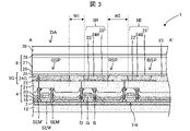
- FIG. 3 is a cross-sectional view showing a schematic configuration of the display device 1 of Embodiment 1 taken along line A-A' shown in FIG.
- a barrier layer 3 As shown in FIG. 3, in the display area DA of the display device 1, a barrier layer 3, a thin film transistor layer 4 including a transistor TR, a red light emitting element 5R, a green light emitting element 5G, and a blue light emitting element 5B are formed on a substrate 12. Also, an edge cover layer 23, a sealing layer 6, and a functional film 39 are provided in this order from the substrate 12 side.
- the green sub-pixels GSP provided in the display area DA of the display device 1 include green light-emitting elements 5G (first light-emitting elements), and the red sub-pixels RSP provided in the display area DA of the display device 1 include red light-emitting elements 5R (
- the blue sub-pixel BSP provided in the display area DA of the display device 1 includes the blue light emitting element 5B (third light emitting element).
- a green light emitting element 5G included in the green subpixel GSP includes a first electrode 22 (anode), a functional layer 24G including a green light emitting layer, and a second electrode 25 (cathode), and is included in the red subpixel RSP.
- the red light emitting element 5R includes a first electrode 22 (anode), a functional layer 24R including a red light emitting layer, and a second electrode 25 (cathode). It includes one electrode 22 (anode), a functional layer 24B including a blue light-emitting layer, and a second electrode 25 (cathode).
- the substrate 12 may be, for example, a resin substrate made of a resin material such as polyimide, or may be a glass substrate.
- a resin substrate made of a resin material such as polyimide is used as the substrate 12 will be described as an example, but the present invention is limited to this. never.
- a glass substrate can be used as the substrate 12 when the display device 1 is a non-flexible display device.
- the barrier layer 3 is a layer that prevents foreign substances such as water and oxygen from entering the transistor TR, the red light emitting element 5R, the green light emitting element 5G, and the blue light emitting element 5B.
- a film, a silicon nitride film, a silicon oxynitride film, or a laminated film of these can be used.
- the transistor TR portion of the thin film transistor layer 4 including the transistor TR includes the semiconductor film SEM and the doped semiconductor films SEM' and SEM'', the inorganic insulating film 16, the gate electrode G, the inorganic insulating film 18, and the inorganic insulating film. 20 , a source electrode S and a drain electrode D, and a planarizing film 21 , and the portion other than the transistor TR portion of the thin film transistor layer 4 including the transistor TR is composed of an inorganic insulating film 16 , an inorganic insulating film 18 , an inorganic insulating film 18 , and an inorganic insulating film 18 . It includes a film 20 and a planarizing film 21 .
- the semiconductor films SEM, SEM', and SEM'' may be composed of, for example, low-temperature polysilicon (LTPS) or an oxide semiconductor (for example, an In--Ga--Zn--O based semiconductor).
- LTPS low-temperature polysilicon
- oxide semiconductor for example, an In--Ga--Zn--O based semiconductor.
- the transistor TR may have a bottom-gate structure.
- the gate electrode G, the source electrode S, and the drain electrode D can be composed of, for example, a single-layer or laminated film of metal containing at least one of aluminum, tungsten, molybdenum, tantalum, chromium, titanium, and copper.
- the inorganic insulating film 16, the inorganic insulating film 18, and the inorganic insulating film 20 can be composed of, for example, a silicon oxide film, a silicon nitride film, a silicon oxynitride film, or a laminated film thereof formed by the CVD method.
- the planarizing film 21 can be made of a coatable organic material such as polyimide or acryl.
- the green light emitting element 5G includes a first electrode 22 (anode) above the planarizing film 21, a functional layer 24G including a green light emitting layer, and a second electrode 25 (cathode).
- the blue light emitting element 5B includes a first electrode 22 (anode) above the planarizing film 21, a functional layer 24R including a red light emitting layer, and a second electrode 25 (cathode). It includes an upper first electrode 22 (anode), a functional layer 24B including a blue light-emitting layer, and a second electrode 25 (cathode).
- the insulating edge cover layer 23 covering the edge of the first electrode 22 (anode) can be formed, for example, by applying an organic material such as polyimide or acrylic and then patterning it by photolithography.
- the functional layer 24G including a green light-emitting layer is configured by stacking, for example, a hole injection layer, a hole transport layer, a green light-emitting layer, an electron transport layer, and an electron injection layer in this order from the first electrode 22 (anode) side. can do.
- One or more of the hole injection layer, the hole transport layer, the electron transport layer and the electron injection layer other than the green light emitting layer in the functional layer 24G including the green light emitting layer may be omitted as appropriate.
- the functional layer 24G including the green light emitting layer is laminated with a hole injection layer, a hole transport layer, a green light emitting layer, an electron transport layer and an electron injection layer in this order from the first electrode 22 (anode) side.
- the functional layer 24R including a red light-emitting layer is configured, for example, by laminating a hole injection layer, a hole transport layer, a red light-emitting layer, an electron transport layer, and an electron injection layer in this order from the first electrode 22 (anode) side. can do.
- the functional layers 24R including the red light emitting layer one or more of the hole injection layer other than the red light emitting layer, the hole transport layer, the electron transport layer, and the electron injection layer may be omitted as appropriate.
- the functional layer 24R including the red light emitting layer is laminated with a hole injection layer, a hole transport layer, a red light emitting layer, an electron transport layer and an electron injection layer in this order from the first electrode 22 (anode) side.
- a hole injection layer a hole transport layer, a red light emitting layer, an electron transport layer and an electron injection layer in this order from the first electrode 22 (anode) side.
- the functional layer 24B including a blue light-emitting layer is configured, for example, by laminating a hole injection layer, a hole transport layer, a blue light-emitting layer, an electron transport layer, and an electron injection layer in this order from the first electrode 22 (anode) side. can do.
- One or more of the hole injection layer, the hole transport layer, the electron transport layer and the electron injection layer other than the blue light emitting layer in the functional layer 24B including the blue light emitting layer may be omitted as appropriate.
- the functional layer 24B including the blue light-emitting layer is laminated with a hole injection layer, a hole transport layer, a blue light-emitting layer, an electron transport layer and an electron injection layer in this order from the first electrode 22 (anode) side.
- a hole injection layer a hole transport layer, a blue light-emitting layer, an electron transport layer and an electron injection layer in this order from the first electrode 22 (anode) side.
- each of the functional layer 24R including the red light-emitting layer, the functional layer 24G including the green light-emitting layer, and the functional layer 24B including the blue light-emitting layer is formed by the same process using the same material.
- a hole injection layer, a hole transport layer formed in the same process using the same material, an electron transport layer formed in the same process using the same material, and electrons formed in the same process using the same material An injection layer will be described as an example, but the present invention is not limited to this.
- the hole injection layers included in the functional layers 24R, 24G, and 24B may be made of different materials.
- the included hole injection layers may be formed in the same process using the same material, and only the hole injection layer included in the remaining one functional layer may be formed in a separate process using a different material.
- the hole transport layers included in the functional layers 24R, 24G, and 24B may be formed of different materials.
- the hole transport layers included in each may be formed in the same process using the same material, and only the hole transport layer included in the remaining one functional layer may be formed in a separate process using a different material.
- each electron transport layer included in each of the functional layers 24R, 24G, and 24B may be formed of different materials. may be formed in the same process using the same material, and only the electron transport layer contained in the remaining one functional layer may be formed in a separate process using a different material.
- each electron injection layer included in each of the functional layers 24R, 24G, and 24B may be formed of different materials. may be formed in the same step using the same material, and only the electron injection layer included in the remaining one functional layer may be formed in a separate step using a different material.
- a control circuit including a transistor TR for controlling each of the red light emitting element 5R, the green light emitting element 5G and the blue light emitting element 5B includes a thin film transistor layer 4 including a transistor TR for each of the red sub-pixel RSP, the green sub-pixel GSP and the blue sub-pixel BSP. is provided in A control circuit including a transistor TR provided for each of the red sub-pixel RSP, the green sub-pixel GSP, and the blue sub-pixel BSP and the light emitting element are also collectively referred to as a sub-pixel circuit.
- the red light emitting element 5R, the green light emitting element 5G and the blue light emitting element 5B shown in FIG. 3 may be of top emission type or bottom emission type.
- the red light emitting element 5R, the green light emitting element 5G, and the blue light emitting element 5B are composed of, from the substrate 12 side, a first electrode 22 (anode), functional layers 24R, 24G, and 24B, and a second electrode 25 (cathode). Since it has a stacked structure formed in order, the second electrode 25 (cathode) is arranged as an upper layer than the first electrode 22 (anode). is made of an electrode material that reflects visible light, and the second electrode 25 (cathode) is made of an electrode material that transmits visible light.
- the second electrode 25 may be formed of an electrode material that transmits visible light
- the second electrode 25 may be formed of an electrode material that reflects visible light.
- the red light emitting element 5R, the green light emitting element 5G, and the blue light emitting element 5B are composed of, from the substrate 12 side, a first electrode 22 (cathode), functional layers 24R, 24G, and 24B, and a second electrode. 25 (anode) are formed in this order, the second electrode 25 (anode) is arranged as an upper layer than the first electrode 22 (cathode).
- the first electrode 22 (cathode) is made of an electrode material that reflects visible light
- the second electrode 25 (anode) is made of an electrode material that transmits visible light
- the second electrode 25 should be made of an electrode material that reflects visible light
- the first electrode 22 (cathode) should be made of an electrode material that transmits visible light.
- the electrode material that reflects visible light is not particularly limited as long as it can reflect visible light and has electrical conductivity. , a laminate of the metal material and a transparent metal oxide (e.g., indium tin oxide, indium zinc oxide, indium gallium zinc oxide, etc.), or a laminate of the alloy and the transparent metal oxide. .
- a transparent metal oxide e.g., indium tin oxide, indium zinc oxide, indium gallium zinc oxide, etc.
- the electrode material that transmits visible light is not particularly limited as long as it can transmit visible light and has electrical conductivity. zinc oxide, etc.) or thin films made of metal materials such as Al, Mg, Li and Ag.
- a film formation method for the first electrode 22 (anode) and the second electrode 25 (cathode) a general electrode formation method can be used.
- a physical vapor deposition (PVD) method such as a coating method, or a chemical vapor deposition (CVD) method can be mentioned.
- the patterning method for the first electrode 22 (anode) and the second electrode 25 (cathode) is not particularly limited as long as it is a method capable of forming a desired pattern with high accuracy. can include a photolithography method, an inkjet method, and the like.
- the sealing layer 6 is a translucent film, and includes, for example, an inorganic sealing film 26 covering the second electrode 25 (cathode), an organic film 27 above the inorganic sealing film 26, and a layer above the organic film 27. , and the inorganic sealing film 28.
- the sealing layer 6 prevents foreign substances such as water and oxygen from penetrating into the red light emitting element 5R, the green light emitting element 5G and the blue light emitting element 5B.
- Each of the inorganic sealing film 26 and the inorganic sealing film 28 is an inorganic film, and may be composed of, for example, a silicon oxide film, a silicon nitride film, a silicon oxynitride film, or a laminated film thereof formed by a CVD method. can be done.
- the organic film 27 is a light-transmitting organic film having a flattening effect, and can be made of a coatable organic material such as acryl.
- the organic film 27 may be formed by, for example, an inkjet method.
- the sealing layer 6 is formed of two layers of inorganic films and one layer of organic film provided between the two layers of inorganic films has been described as an example.
- the sealing layer 6 may be composed of only an inorganic film, may be composed of only an organic film, may be composed of one layer of inorganic film and two layers of organic film, or may be composed of two or more layers. may be composed of an inorganic film and two or more layers of organic films.
- the functional film 39 is, for example, a film having at least one of optical compensation function, touch sensor function, and protection function.
- the first contact surface formed by contact between the first electrode 22 of the green light emitting element 5G and the functional layer 24G including the green light emitting layer and the contact surface of the green light emitting element 5R is equal to the first electrode 22 of the blue light emitting element 5B.
- a second direction YD orthogonal to the first direction XD between a third contact surface formed in contact with the functional layer 24B including a blue light emitting layer and at least one of the first contact surface and the second contact surface is smaller than the shortest width W2 along
- the second direction YD between the third contact surface and at least one of the first contact surface and the second contact surface is relatively large, for example 22 ⁇ m.
- the shortest width W1 along the first direction XD of is set relatively small, for example, 18 ⁇ m.
- the displacement amount YD' in the second direction YD perpendicular to the extending directions KD/KD' of the plurality of vapor deposition openings MK of each divided mask DM as described above is When forming at least one of a green light-emitting layer, a red light-emitting layer, and a blue light-emitting layer using a vapor deposition mask larger than a displacement amount XD' in a certain first direction XD, the area of the light-emitting region in one pixel is unnecessarily increased. A wider process margin (product design margin) can be secured without narrowing.
- the shortest width W2 is 22 ⁇ m and the shortest width W1 is 18 ⁇ m.
- the value of shortest width W2/shortest width W1 is preferably 1.2 or more and 1.5 or less.
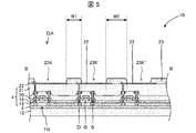
- FIG. 4 is a schematic view of the active matrix substrate 10 including the first opening 23K, the second opening 23K' and the third opening 23K'' including the edge cover layer 23, which is included in the display device 1 of the first embodiment.
- 1 is a plan view showing a configuration
- FIG. 5 is a cross-sectional view showing a schematic configuration of the active matrix substrate 10 along line B-B' shown in FIG.
- FIG. 6 shows a state after forming a hole transport layer 24HT, a green light emitting layer 24GH, a red light emitting layer 24RH, and a blue light emitting layer 24BH in this order on the active matrix substrate 10 shown in FIGS.
- FIG. 4 is a diagram showing;
- a manufacturing method of a display device 1 having a plurality of pixels PIX each including a green light emitting element 5G, a red light emitting element 5R, and a blue light emitting element 5B on a substrate 12 includes, as shown in FIG.
- a second electrode 25 is formed on the functional layer 24G including the light emitting layer 24GH, on the functional layer 24R including the red light emitting layer 24RH of the red light emitting element 5R, and on the functional layer 24B including the blue light emitting layer 24BH of the blue light emitting element 5B. and forming a second electrode.
- the first electrode 22 of the green light emitting element 5G, the first electrode 22 of the red light emitting element 5R, and the blue light emitting element 5B As shown in FIGS. 4 and 5, in the edge cover layer forming step of forming the edge cover layer 23, the first electrode 22 of the green light emitting element 5G, the first electrode 22 of the red light emitting element 5R, and the blue light emitting element 5B.
- the third openings 23K'' are arranged adjacent to each other for each pixel PIX in one of row and N row (the N is an even number of 2 or more), and the third openings 23K'' are arranged in the N-1 row and the N row.
- the shortest width W1 along the first direction XD between the first opening 23K and the second opening 23K' is the shortest width W1 between the third opening 23K'' and the first opening 23K and the second opening 23K'.
- An edge cover layer 23 smaller than the shortest width W2 along the second direction YD orthogonal to the first direction XD between at least one of the two openings 23K' is formed.
- the first opening 23K of the edge cover layer 23 has the same shape as the first contact surface formed by contact between the first electrode 22 of the green light emitting element 5G and the functional layer 24G including the green light emitting layer.
- the second opening 23K' of the edge cover layer 23 has the same shape as the second contact surface formed by contact between the first electrode 22 of the red light emitting element 5R and the functional layer 24R including the red light emitting layer.
- the third opening 23K'' of the edge cover layer 23 has the same shape as the third contact surface formed by contact between the first electrode 22 of the blue light emitting element 5B and the functional layer 24B including the blue light emitting layer. be.
- the green light emitting element 5G including the first contact surface and the red light emitting element 5R including the second contact surface are arranged in N ⁇ 1 rows and N rows (where N is an even number of 2 or more) along the first direction XD. ) so as to be adjacent to each other for each pixel PIX, and the blue light emitting element 5B including the third contact surface is arranged for each pixel PIX on the other of the N ⁇ 1 row and the N row. It is
- the shortest width W2 along the first opening 23K and the second opening 23K' is set relatively large, for example, 22 ⁇ m.
- the shortest width W1 along one direction XD is set relatively small, for example, 18 ⁇ m.
- the displacement amount YD' in the second direction YD orthogonal to the extending directions KD and KD' of the plurality of vapor deposition openings MK of each divided mask DM as described above is ,
- a green light-emitting layer, a red light-emitting layer, and a blue light-emitting layer using a vapor deposition mask larger than the displacement amount XD' in the first direction XD, which is the stretching direction KD ⁇ KD', within one pixel It is possible to ensure a wider process margin (product design margin) without unnecessarily narrowing the area of the light emitting region.
- the shortest width W2 along the second direction YD between the third opening 23K'' and at least one of the first opening 23K and the second opening 23K' is 22 ⁇ m, and the first opening 23K and the second opening 23K′ in the first direction XD is 18 ⁇ m, but the present invention is not limited to this.
- the value of shortest width W2/shortest width W1 is preferably 1.2 or more and 1.5 or less.
- the first opening 23K and the second opening 23K' are arranged along the first direction XD in the first row GY1, the third row GY3, the fifth row GY5, and the seventh row.
- Pixels PIX are arranged adjacent to each other in odd-numbered rows such as GY7 and ninth row GY9, and the third openings 23K'' are arranged along the first direction XD in the second row GY2, the fourth row GY4, the sixth row GY4, and the sixth row GY9.
- a case where pixels PIX are arranged in even-numbered rows such as row GY6, eighth row GY8, and tenth row GY10 will be described as an example, but the present invention is not limited to this.
- the width in the first direction XD of the third openings 23K'' of the edge cover layer 23 is the width of the first openings 23K in the edge cover layer 23 in the first direction XD. Width obtained by adding one of the widths in the first direction XD of the second openings 23K' of the edge cover layer 23 and the shortest width W1 along the first direction XD between the first openings 23K and the second openings 23K' Larger, the first opening 23K and the second opening 23K' are arranged in odd rows such as the first row GY1, the third row GY3, the fifth row GY5, the seventh row GY7 and the ninth row GY9 along the first direction XD. are arranged alternately.
- the width in the first direction XD of the third contact surface formed by contact between the first electrode 22 of the blue light emitting element 5B and the functional layer 24B including the blue light emitting layer is the same as that of the green light emitting element 5G.
- the green light emitting element 5G including the first contact surface and the red light emitting element 5R including the second contact surface are arranged in a first row GY1 and a third row GY3 along the first direction XD.
- 5th row GY5, 7th row GY7, and 9th row GY9 are alternately arranged in odd-numbered rows.
- the size of the third contact surface formed by contact between the first electrode 22 of the blue light emitting element 5B and the functional layer 24B including the blue light emitting layer is the same as that of the first electrode 22 of the green light emitting element 5G. and the functional layer 24G including the green light emitting layer, and the contact surface between the first electrode 22 of the red light emitting element 5R and the functional layer 24R including the red light emitting layer.
- a case where the size is larger than the size of the second contact surface to be formed will be described as an example, but the present invention is not limited to this.
- the first pixel PIX, the second pixel PIX, and the third pixel PIX are three adjacent pixels arranged in this order along the first direction XD.
- the shortest width W3 along the first direction XD is the third opening 23K'' of the edge cover layer 23 included in the other of the first pixel PIX and the third pixel PIX and the third opening 23K'' of the edge cover layer 23 included in the second pixel PIX.
- the shortest width W3 along the first direction XD between the first electrode 22 and the third contact surface formed by contacting the functional layer 24B including the blue light emitting layer is the distance between the first pixel PIX and the third pixel PIX.
- a case where the shortest width W4 along the first direction XD between the first electrode 22 and the functional layer 24B including the blue light emitting layer is in contact with the third contact surface formed by contacting the first electrode 22 and the functional layer 24B including the blue light emitting layer is described as an example. , but not limited to this.
- a light-emitting layer 24BH was formed in this order as follows.
- the step of forming the green light emitting layer 24GH as shown in FIG.
- the first electrode 22 of the green light emitting element 5G exposed through the first opening 23K using a vapor deposition mask M that has an opening MK and is stretched in the first direction XD and in the direction opposite to the first direction XD.
- a green light emitting layer 24GH was formed thereon.
- the deposition area of the green light emitting layer 24GH is indicated by dotted lines.
- the same shape and pitch are formed in the same manner as the vapor deposition mask M shown in FIG.
- a vapor deposition mask for the red light emitting layer 24RH that has a plurality of vapor deposition openings formed by A red light-emitting layer 24RH was formed on the first electrode 22 of the red light-emitting element 5R exposed through.
- the deposition area of the red light emitting layer 24RH is indicated by dotted lines.
- the same shape and pitch are formed in the same manner as the vapor deposition mask M shown in FIG.
- a vapor deposition mask for the blue light emitting layer 24BH which has a plurality of vapor deposition openings formed in the above manner and which is stretched in the first direction XD and the direction opposite to the first direction XD, the third openings 23K' are formed.
- a blue light-emitting layer 24BH is formed on the first electrode 22 of the blue light-emitting element 5B exposed through '.
- the deposition area of the blue light emitting layer 24BH is indicated by dotted lines.
- the green light emitting layer 24GH, the red light emitting layer 24RH, and the blue light emitting layer 24BH are formed in this order will be described as an example, but the present invention is not limited to this. can be formed in any order.
- FIG. 10 is a diagram for explaining the reason why a margin can be secured
- FIG. 7(a) shows the vapor deposition region of the red light emitting layer 24RH when there is almost no misalignment (fluctuation) amount YD' of alignment in the second direction YD of the plurality of vapor deposition openings of the vapor deposition mask for the red light emitting layer 24RH. show.
- FIG. 7 shows the case where the amount of misalignment (fluctuation) YD′ of the plurality of vapor deposition openings of the vapor deposition mask for the red light emitting layer 24RH in the second direction YD is the maximum permissible upward direction in the figure. 2 shows the vapor deposition region of the red light emitting layer 24RH.
- the red light emitting layer 24RH is vapor-deposited in the third opening 23K'' of the edge cover layer 23, color mixture occurs in the blue light emitting element 5B, or the second opening of the edge cover layer 23
- the red light emitting layer 24RH is not vapor-deposited on a part of 23K', and the light emitting region of the red light emitting element 5R is narrowed.
- FIG. 7 shows the case where the amount of misalignment (fluctuation) YD′ of the plurality of vapor deposition openings of the vapor deposition mask for the red light emitting layer 24RH in the second direction YD is the maximum permissible downward direction in the figure. 2 shows the vapor deposition region of the red light emitting layer 24RH.
- the red light emitting layer 24RH is vapor-deposited in the third opening 23K'' of the edge cover layer 23, color mixture occurs in the blue light emitting element 5B, or the second opening of the edge cover layer 23
- the red light emitting layer 24RH is not vapor-deposited on a part of 23K', and the light emitting region of the red light emitting element 5R is narrowed.
- the shortest width W2 along the second direction YD between the third opening 23K'' and at least one of the first opening 23K and the second opening 23K' is set relatively large, for example, 22 ⁇ m. Therefore, a wider process margin (product design margin) can be ensured in the process of forming the red light emitting layer 24RH.
- FIG. 10 is a diagram for explaining the reason why a margin can be secured
- FIG. 8 shows the vapor deposition of the green light emitting layer 24GH when there is almost no misalignment (fluctuation) amount YD' of alignment in the second direction YD of the plurality of vapor deposition openings MK of the vapor deposition mask M for the green light emitting layer 24GH. indicate the area.
- FIG. 8 shows that the alignment deviation (fluctuation) amount YD′ of the plurality of vapor deposition openings MK of the vapor deposition mask M for the green light emitting layer 24GH in the second direction YD is the maximum permissible value in the upper direction in the figure.
- FIG. 4 shows the deposition area of green light emitting layer 24GH in one case.
- the green light emitting layer 24GH is vapor-deposited in the third opening 23K'' of the edge cover layer 23, color mixture occurs in the blue light emitting element 5B, or the first opening of the edge cover layer 23
- the green light-emitting layer 24GH is not vapor-deposited on a part of 23K, and the light-emitting region of the green light-emitting element 5G is narrowed.
- FIG. 8 shows that the amount of misalignment (fluctuation) YD′ of the plurality of vapor deposition openings MK of the vapor deposition mask M for the green light emitting layer 24GH in the second direction YD is the maximum permissible downward direction in the figure.
- FIG. 4 shows the deposition area of green light emitting layer 24GH in one case.
- the green light emitting layer 24GH is vapor-deposited in the third opening 23K'' of the edge cover layer 23, color mixture occurs in the blue light emitting element 5B, or the first opening of the edge cover layer 23
- the green light-emitting layer 24GH is not vapor-deposited on a part of 23K, and the light-emitting region of the green light-emitting element 5G is narrowed.
- the shortest width W2 along the second direction YD between the third opening 23K'' and at least one of the first opening 23K and the second opening 23K' is set relatively large, for example, 22 ⁇ m. Therefore, a wider process margin (product design margin) can be ensured in the process of forming the green light emitting layer 24GH.
- FIG. 10 is a diagram for explaining the reason why a margin can be secured
- FIG. 9 shows the vapor deposition region of the blue light emitting layer 24BH when there is almost no misalignment (fluctuation) amount YD' of alignment in the second direction YD of the plurality of vapor deposition openings of the vapor deposition mask for the blue light emitting layer 24BH. show.
- FIG. 9 shows the case where the amount of misalignment (fluctuation) YD′ of the plurality of vapor deposition openings of the vapor deposition mask for the blue light emitting layer 24BH in the second direction YD is the maximum permissible value in the upper direction in the figure. 2 shows the vapor deposition region of the blue light emitting layer 24BH. If the permissible maximum value is exceeded, the blue light emitting layer 24BH is vapor-deposited in the first opening 23K and the second opening 23K' of the edge cover layer 23, causing color mixture between the green light emitting element 5G and the red light emitting element 5R. , the blue light-emitting layer 24BH is not vapor-deposited in a part of the third opening 23K'' of the edge cover layer 23, and the light-emitting region of the blue light-emitting element 5B is narrowed.
- FIG. 9 shows the case where the amount of misalignment (fluctuation) YD′ of the plurality of vapor deposition openings of the vapor deposition mask for the blue light emitting layer 24BH in the second direction YD is the maximum permissible downward direction in the figure. 2 shows the vapor deposition region of the blue light emitting layer 24BH. If the permissible maximum value is exceeded, the blue light emitting layer 24BH is vapor-deposited in the first opening 23K and the second opening 23K' of the edge cover layer 23, causing color mixture between the green light emitting element 5G and the red light emitting element 5R. , the blue light-emitting layer 24BH is not vapor-deposited in a part of the third opening 23K'' of the edge cover layer 23, and the light-emitting region of the blue light-emitting element 5B is narrowed.
- the shortest width W2 along the second direction YD between the third opening 23K'' and at least one of the first opening 23K and the second opening 23K' is set relatively large, for example, 22 ⁇ m. Therefore, a wider process margin (product design margin) can be ensured in the process of forming the blue light emitting layer 24BH.
- three vapor deposition masks (a green light emitting layer vapor deposition mask, a red light emitting layer vapor deposition mask, and a blue light emitting layer vapor deposition mask) having the size shown in FIG. ) to form a green light emitting layer 24GH, a red light emitting layer 24RH, and a blue light emitting layer 24BH in a large display panel.
- a large display panel includes a plurality of display devices 1, and a plurality of display devices 1 can be obtained by performing a dividing step for dividing such a large display panel.
- the shortest width W2 is 22 ⁇ m and the shortest width W1 along the first direction XD between the first opening 23K and the second opening 23K′ is 18 ⁇ m, that is, the value of the shortest width W2/shortest width W1 is the large
- the shortest width W2 is The values of shortest width W2/shortest width W1 of each display device included in the large display panel may be different as long as they are larger than the shortest width W1.
- FIG. 10 a second embodiment of the present invention will be described with reference to FIGS. 10 and 11.
- FIG. 10 the values of the shortest width W2/shortest width W1 of some of the display devices are different from the above-described Embodiment 1. different. Others are as described in the first embodiment.
- members having the same functions as the members shown in the drawings of the first embodiment are denoted by the same reference numerals, and the explanation thereof is omitted.
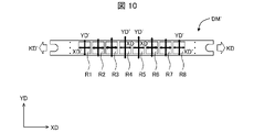
- FIG. 10 is a plan view showing a schematic configuration of the divided mask DM' included in the vapor deposition mask used in the manufacturing process of the display panel 50 of the second embodiment.
- the divided mask DM' shown in FIG. 10 includes the first vapor deposition opening group R1 to the eighth vapor deposition opening group R8, one divided mask DM' corresponds to eight display devices. is doing.
- the alignment deviation amount YD' in the second direction YD of the plurality of deposition openings of the divided mask DM' is It becomes larger as it goes from both ends of XD to the central part. That is, the alignment deviation amount YD′ in the second direction YD of the plurality of vapor deposition openings belonging to the fourth vapor deposition opening group R4 and the fifth vapor deposition opening group R5 is It is larger than the misalignment amount YD' of the plurality of vapor deposition openings belonging to the opening group R8 in the second direction YD.
- the alignment deviation amount YD′ in the second direction YD of the plurality of vapor deposition openings belonging to the second vapor deposition opening group R2 and the seventh vapor deposition opening group R7 is the same as that for the first vapor deposition opening group R1 and the eight vapor deposition opening group
- the alignment deviation amount YD′ in the second direction YD of the plurality of vapor deposition openings belonging to the opening group R8 is larger than the alignment deviation amount YD′ of the plurality of vapor deposition openings belonging to the third vapor deposition opening group R3 and the sixth vapor deposition opening group R6.
- the alignment deviation amount YD' in the direction YD is larger than the alignment deviation amount YD' in the second direction YD of the vapor deposition openings belonging to the second vapor deposition opening group R2 and the seventh vapor deposition opening group R7.
- the amount of misalignment (fluctuation) XD' of the plurality of deposition openings in the divided mask DM' in the first direction XD is the same at both ends in the first direction XD of the divided mask DM' No big difference. That is, there is no significant difference in the alignment deviation (sway) amount XD' in the first direction XD of the vapor deposition openings belonging to the first vapor deposition opening group R1 to the eight vapor deposition opening group R8.
- a vapor deposition mask including a plurality of divided masks DM' shown in FIG. 10 will be described as an example.
- a vapor deposition mask including a plurality of divided masks DM' shown in FIG. 10 may be used, which includes a plurality of divided masks DM.
- FIG. 11 is a plan view showing a schematic configuration of the display panel 50 of Embodiment 2.
- FIG. 11 is a plan view showing a schematic configuration of the display panel 50 of Embodiment 2.
- the display panel 50 includes a plurality of display devices 1A-1H. Substrates provided in each of the plurality of display devices 1A to 1H are integrally formed.
- the plurality of display devices 1A to 1H includes a display device 1A as a first display device, a display device 1D and a display device 1E as second display devices, and a display device 1H as a third display device.
- the value of the shortest width W2/shortest width W1 in each pixel PIX of the display device 1D and the display device 1E, which are two display devices, is the shortest width W2′/shortest width W1 in each pixel PIX of the display device 1A, which is the first display device.
- the display device 1H which is the third display device, is arranged at the end of the substrate integrally formed on one side in the first direction XD, and the display device 1H is arranged at the end of the substrate formed integrally on the other side in the first direction XD.
- the display device 1D and the display device 1E which are display devices, are arranged at an intermediate position between the display device 1A, which is the first display device, and the display device 1H, which is the third display device.
- shortest width W2 along the second direction YD is 27 ⁇ m
- the shortest width W1 along the first direction XD between the first opening 23K and the second opening 23K′ is 18 ⁇ m. That is, the value of shortest width W2/shortest width W1 was set to 1.5.
- the second display device between the third opening 23L'' and at least one of the first opening 23L and the second opening 23L'.
- the shortest width W2′ along the direction YD is 22 ⁇ m
- the shortest width W1′ along the first direction XD between the first opening 23L and the second opening 23L′ is 18 ⁇ m. That is, the value of shortest width W2'/shortest width W1' was set to about 1.2.
- a display device 1B and a display device 1C are further provided between the display device 1A as the first display device and the display device 1D as the second display device, and are the third display device.
- a display device 1F and a display device 1G are further provided between the display device 1H and the display device 1E, which is the second display device.
- the value of shortest width W2/shortest width W1 in each pixel PIX of display device 1B is set to 1.3
- the value of shortest width W2/shortest width W1 in each pixel PIX of display device 1C is set to 1.4.
- the value of the shortest width W2/shortest width W1 in each pixel PIX of the display devices 1B and 1C becomes the shortest width W2/shortest width in each pixel PIX of the display device 1D.
- the value of W1, which is 1.5, may be approached step by step.
- the value of shortest width W2/shortest width W1 in each pixel PIX of display device 1G is set to 1.3
- the value of shortest width W2/shortest width W1 in each pixel PIX of display device 1F is set to 1.3.
- the value of the shortest width W2/the shortest width W1 in each pixel PIX of the display devices 1F and 1G becomes closer to the shortest width W2 in each pixel PIX of the display device 1E.
- the value of the shortest width W1, ie, 1.5, may be approached step by step.
- the sizes of the first openings 23K and 23L that is, the first electrodes 22 of the green light emitting elements 5G and the functional layers 24G including the green light emitting layers are the same, and the sizes of the second openings 23K′ and 23L′, that is, the functions including the first electrode 22 of the red light emitting element 5R and the red light emitting layer, are the same.
- the sizes of the second contact surfaces formed in contact with the layer 24R are the same, and the sizes of the third openings 23K'' and 23L'', that is, the first electrode 22 of the blue light emitting element 5B and the blue light emitting element 5B, have the same size.
- the sizes of the third contact surfaces formed in contact with the functional layer 24B including the light emitting layer are the same.
- the shape of the first openings 23K and 23L that is, the first electrode 22 of the green light emitting element 5G and the functional layer 24G including the green light emitting layer are formed in contact with each other.
- the shapes of the second openings 23K′ and 23L′ that is, the first electrode 22 of the red light emitting element 5R and the functional layer 24R including the red light emitting layer are formed in contact with each other.
- the shapes of the second contact surfaces are different, and the shapes of the third openings 23K'' and 23L'', that is, the first electrodes 22 of the blue light emitting elements 5B and the functional layers 24B including the blue light emitting layers are formed in contact with each other.
- the shape of the third contact surface is different.
- each pixel PIX in one display device 1A to 1H has the same value of shortest width W2/shortest width W1, but it is not limited to this.
- each pixel PIX of each of the plurality of display devices 1A to 1H included in the display panel 50 the light emitting area of the light emitting layer of each color can be made the same, and the large display panel 50 can be divided.
- the display devices 1A to 1H thus obtained are display devices of the same grade.
- a vapor deposition mask including a plurality of divided masks DM' shown in FIG. 10 will be described as an example.
- a vapor deposition mask including a plurality of divided masks DM' shown in FIG. 10 may be used, which includes a plurality of divided masks DM.
- FIG. 12 is a plan view showing a schematic configuration of the display panel 50' of the third embodiment.
- the display panel 50' includes a plurality of display devices 1A' to 1H'. Substrates provided in each of the plurality of display devices 1A' to 1H' are integrally formed.
- the plurality of display devices 1A' to 1H' includes a display device 1A' as a first display device, a display device 1D' and a display device 1E' as second display devices, and a display device 1H as a third display device.
- a display device 1A' as a first display device
- a display device 1D' and a display device 1E' as second display devices
- a display device 1H as a third display device.
- the value of the shortest width W2''/shortest width W1'' in each pixel PIX of the display device 1D' and the display device 1E' that are the second display device is the display device 1A' that is the first display device.
- the shortest width W2'''/shortest width W1''' of each pixel PIX of the display device 1H' which is the third display device.
- the display device 1A' which is the first display device, is disposed at one end of the integrally formed substrate in the first direction XD
- the display device 1H' which is the third display device
- a display device 1D′ and a display device 1E′ which are second display devices, are arranged at the end portion of the substrate formed integrally on the other side in the first direction XD
- the display device 1A′ which is a first display device. It is arranged at an intermediate position between the display device 1H' which is the third display device.
- the size of the first opening 23M in each pixel PIX of the display device 1D' and the display device 1E' which are the second display devices, that is, the first electrode 22 of the green light emitting element 5G and the functional layer 24G including the green light emitting layer and the size of the second opening 23M′, that is, the first electrode 22 of the red light emitting element 5R and the functional layer 24R including the red light emitting layer are in contact with each other.
- the size of the third opening 23M'' that is, the third contact surface formed by contacting the first electrode 22 of the blue light emitting element 5B and the functional layer 24B including the blue light emitting layer.
- the size combined with the size of the contact surface is the size of the first opening 23N in each pixel PIX of the display device 1A' which is the first display device and the display device 1H' which is the third display device, that is, the green color.
- the size of the first contact surface formed by contact between the first electrode 22 of the light emitting element 5G and the functional layer 24G including the green light emitting layer and the size of the second opening 23N' The size of the second contact surface formed by contact between the first electrode 22 and the functional layer 24R including the red light emitting layer and the size of the third opening 23N'', that is, the first electrode 22 of the blue light emitting element 5B It is smaller than the combined size of the third contact surface formed in contact with the functional layer 24B including the blue light emitting layer.
- the third opening 23M'' and at least one of the first opening 23M and the second opening 23M' is 18 ⁇ m along the first direction XD. That is, the value of shortest width W2''/shortest width W1'' was set to 1.5.
- the gap between the third opening 23N'' and at least one of the first opening 23N and the second opening 23N' is 22 ⁇ m
- the shortest width W1''' along the first direction XD between the first opening 23N and the second opening 23N' is 18 ⁇ m. That is, the value of shortest width W2'''/shortest width W1''' is set to about 1.2.
- a display device 1B' and a display device 1C' are further provided between the display device 1A' which is the first display device and the display device 1D' which is the second display device.
- a display device 1F' and a display device 1G' are further provided between the display device 1H', which is a display device, and the display device 1E', which is a second display device.
- the value of shortest width W2/shortest width W1 in each pixel PIX of the display device 1B′ is set to 1.3
- the value of shortest width W2/shortest width W1 in each pixel PIX of the display device 1C′ is set to 1.4.
- the value of the shortest width W2/shortest width W1 in each pixel PIX of the display device 1B' and the display device 1C' changes to each pixel PIX of the display device 1D'.
- the value of the shortest width W2''/the shortest width W1'' at which is 1.5, may be approached step by step.
- the value of shortest width W2/shortest width W1 in each pixel PIX of the display device 1G′ is set to 1.3
- the value of shortest width W2/shortest width W1 in each pixel PIX of the display device 1F′ is set to 1.4
- the value of the shortest width W2/shortest width W1 in each pixel PIX of the display device 1F' and the display device 1G' becomes the value of the display device 1E'.
- the value of shortest width W2′′/shortest width W1′′ in each pixel PIX may be approached step by step to 1.5.
- the size of the first opening that is, the size of the first contact surface formed by contact between the first electrode 22 of the green light emitting element 5G and the functional layer 24G including the green light emitting layer
- the size of the second opening That is, the size of the second contact surface formed by contact between the first electrode 22 of the red light emitting element 5R and the functional layer 24R including the red light emitting layer
- the size of the third opening that is, the size of the blue light emitting element 5B
- the total size of the third contact surface formed by the contact between the first electrode 22 and the functional layer 24B including the blue light-emitting layer increases as the display device 1A′ approaches the display device 1D′.
- each pixel PIX of 1D′ may be gradually approached to the sum of the size of the first contact surface, the size of the second contact surface, and the size of the third contact surface.
- the size that is, the size of the first contact surface formed by contact between the first electrode 22 of the green light emitting element 5G and the functional layer 24G including the green light emitting layer, and the size of the second opening, that is, the red light emission
- each pixel PIX in one display device 1A' to 1H' has the same value of shortest width W2/shortest width W1, but it is not limited to this. do not have.
- each pixel PIX of each of the plurality of display devices 1A' to 1H' included in the display panel 50' the light-emitting area of the light-emitting layer of each color can be made different, and a large display can be obtained.
- the dividing step of dividing the panel 50' at least a part of each of the obtained display devices 1A' to 1H' can be display devices of different grades.
- a substrate A first light-emitting element, a second light-emitting element, and a third light-emitting element each provided with a first electrode, a functional layer including a light-emitting layer, and a second electrode in this order from the substrate side on the substrate.
- a plurality of pixels each including the first light emitting element, the second light emitting element, and the third light emitting element; a first contact surface formed by contact between the first electrode of the first light emitting element and the functional layer of the first light emitting element; and the first electrode of the second light emitting element and the second light emitting element.
- the shortest width W1 along the first direction between the second contact surface formed in contact with the functional layer of the first electrode of the third light emitting element and the functional layer of the third light emitting element smaller than the shortest width W2 along the second direction orthogonal to the first direction between a third contact surface formed by contact with and at least one of the first contact surface and the second contact surface, indicated Device.
- the first light emitting element and the second light emitting element are adjacent to each other for each pixel in one of N ⁇ 1 rows and N rows (where N is an even number equal to or greater than 2) along the first direction. is placed in the third light emitting element is arranged for each pixel in the other of the N-1 row and the N row;
- the first light-emitting element includes a first light-emitting layer as the light-emitting layer
- the second light-emitting element includes, as the light-emitting layer, a second light-emitting layer having an emission peak wavelength different from that of the first light-emitting layer
- the width of the third contact surface in the first direction is one of the width of the first contact surface in the first direction and the width of the second contact surface in the first direction, and the shortest width W1. larger than the combined width,
- the first pixel, the second pixel, and the third pixel are three adjacent pixels arranged in this order along the first direction;
- the shortest width W3 along the first direction between the third contact surface included in one of the first pixel and the third pixel and the third contact surface included in the second pixel is Aspects 2 to 4, wherein the shortest width W4 along the first direction between the third contact surface included in the other of the pixel and the third pixel and the third contact surface included in the second pixel is smaller than W4
- a display device any one of the above.
- An edge cover layer covering respective ends of the first electrode of the first light emitting element, the first electrode of the second light emitting element, and the first electrode of the third light emitting element,
- the edge cover layer includes a first opening having the same shape as the first contact surface, a second opening having the same shape as the second contact surface, and a third opening having the same shape as the third contact surface.
- the first light-emitting layer is a light-emitting layer that emits green light
- the second light-emitting layer is a light-emitting layer that emits red light
- the display device according to any one of Modes 2 to 7, wherein the third light-emitting layer is a light-emitting layer that emits blue light.
- a plurality of display devices according to any one of aspects 1 to 8, the substrates included in each of the plurality of display devices are integrally formed, the plurality of display devices includes a first display device, a second display device and a third display device;
- the value of the shortest width W2/the shortest width W1 in each pixel of the second display device is the same as the value of the shortest width W2/the shortest width W1 in each pixel of the first display device and the value of the shortest width W2/the shortest width W1 in each pixel of the third display device.
- the first display device is disposed at one end of the substrate integrally formed in the first direction
- the third display device is disposed at the end of the substrate formed integrally on the other side in the first direction
- the display panel, wherein the second display device is arranged at an intermediate position between the first display device and the third display device.
- the plurality of display devices are further provided between the first display device and the second display device and between the third display device and the second display device, respectively;
- the value of the shortest width W2/the shortest width W1 in each pixel of each of the plurality of display devices provided between the first display device and the second display device is the same as the first display device to the second display device. 2 gradually approaches the value of the shortest width W2/the shortest width W1 in each pixel of the second display device,
- the value of the shortest width W2/the shortest width W1 in each pixel of each of the plurality of display devices provided between the third display device and the second display device is the same as the third display device to the third display device.
- the sum of the size of the first contact surface, the size of the second contact surface, and the size of the third contact surface in each pixel of the second display device is the a sum of the size of the first contact surface, the size of the second contact surface, and the size of the third contact surface; and the size of the first contact surface and the second contact in each pixel of the third display device 11.
- the sum of the size of the first contact surface, the size of the second contact surface, and the size of the third contact surface in each pixel of the second display device is the a sum of the size of the first contact surface, the size of the second contact surface, and the size of the third contact surface; and the size of the first contact surface and the second contact in each pixel of the third display device smaller than the sum of the size of the surface and the size of the third contact surface, The size of the first contact surface, the size of the second contact surface, and the third contact surface in each pixel of each of the plurality of display devices provided between the first display device and the second display device.
- the size of the first contact surface and the size of the second contact surface in each pixel of the second display device increase as the second display device approaches the first display device. stepwise approaching the size combined with the size of the third contact surface, The size of the first contact surface, the size of the second contact surface, and the third contact surface in each pixel of each of the plurality of display devices provided between the third display device and the second display device. The size of the first contact surface and the size of the second contact surface in each pixel of the second display device increase as the third display device approaches the second display device. 11. The display panel according to aspect 10, wherein the size combined with the size of the third contact surface is approached stepwise.
- a method of manufacturing a display device having a plurality of pixels each including a first light emitting element, a second light emitting element, and a third light emitting element on a substrate comprising: a first electrode forming step of forming a first electrode on the substrate; While covering respective ends of the first electrode of the first light emitting element, the first electrode of the second light emitting element, and the first electrode of the third light emitting element, the first electrode of the first light emitting element a first opening exposing a portion of an electrode; a second opening exposing a portion of the first electrode of the second light emitting element; and a third opening exposing a portion of the first electrode of the third light emitting element.
- first opening and the second opening are adjacent to each other for each pixel in one of N ⁇ 1 rows and N rows (where N is an even number equal to or greater than 2) along the first direction.
- the third opening is arranged for each pixel in the other of the N ⁇ 1 rows and the N rows, and the first direction is between the first opening and the second opening. is less than the shortest width W2 along a second direction perpendicular to the first direction between the third opening and at least one of the first and second openings.
- a method of manufacturing a display device comprising: forming two electrodes.
- the light-emitting layer forming step includes It has a plurality of first vapor deposition openings formed corresponding to the positions of the first openings with the same shape and pitch, and is stretched in the first direction and the direction opposite to the first direction.
- a first light emitting layer forming step of forming a first light emitting layer on the first electrode of the first light emitting element exposed through the first opening using a first vapor deposition mask It has a plurality of second vapor deposition openings formed corresponding to the positions of the second openings with the same shape and pitch, and is stretched in the first direction and the direction opposite to the first direction.
- a second light emitting layer having an emission peak wavelength different from that of the first light emitting layer on the first electrode of the second light emitting element exposed through the second opening using a second vapor deposition mask; a light-emitting layer forming step; It has a plurality of third vapor deposition openings formed corresponding to the positions of the third openings with the same shape and pitch, and is stretched in the first direction and the direction opposite to the first direction.
- a method of manufacturing a display device comprising a third light-emitting layer forming step of forming a layer.
- the substrates included in each of the plurality of display devices are integrally formed, the plurality of display devices includes a first display device, a second display device and a third display device;
- the first display device is disposed at one end of the substrate integrally formed in the first direction,
- the third display device is disposed at the end of the substrate formed integrally on the other side in the first direction, the second display device is arranged at an intermediate position between the first display device and the third display device;
- the value of the shortest width W2/the shortest width W1 in each pixel of the second display device is the ratio of the shortest width W2/the shortest width W1 in each pixel of the first display device.
- the plurality of display devices are further provided between the first display device and the second display device and between the third display device and the second display device, respectively;
- the value of the shortest width W2/the shortest width W1 in each pixel of each of the plurality of display devices provided between the first display device and the second display device is , the value of the shortest width W2/the shortest width W1 in each pixel of the second display device gradually approaches the value of the shortest width W2/the shortest width W1 as the distance from the first display device to the second display device increases.
- the sizes of the first openings are the same in all the display devices including the first display device, the second display device, and the third display device, and 18.
- the sum of the size of the first opening, the size of the second opening, and the size of the third opening in each pixel of the second display device is the size of the first display.
- the sum of the size of the first opening, the size of the second opening, and the size of the third opening in each pixel of the second display device is the first opening in each pixel of the first display device.
- the present invention can be used for a display device, a display panel, and a method for manufacturing a display device.
Landscapes
- Physics & Mathematics (AREA)
- General Physics & Mathematics (AREA)
- Engineering & Computer Science (AREA)
- Theoretical Computer Science (AREA)
- Electroluminescent Light Sources (AREA)
Abstract
Description
基板と、
前記基板上に、それぞれが、第1電極と、発光層を含む機能層と、第2電極とを、前記基板側からこの順に備えた、第1発光素子、第2発光素子及び第3発光素子と、
それぞれが、前記第1発光素子と、前記第2発光素子と、前記第3発光素子とを含む複数の画素と、を含み、
前記第1発光素子の前記第1電極と前記第1発光素子の前記機能層とが接触して形成される第1接触面と、前記第2発光素子の前記第1電極と前記第2発光素子の前記機能層とが接触して形成される第2接触面との間の第1方向に沿う最短幅W1は、前記第3発光素子の前記第1電極と前記第3発光素子の前記機能層とが接触して形成される第3接触面と前記第1接触面及び前記第2接触面の少なくとも一方との間の前記第1方向と直交する第2方向に沿う最短幅W2より小さい。
前記表示装置を複数個備え、
前記複数個の表示装置のそれぞれが備える前記基板は一体として形成されており、
前記複数個の表示装置は、第1表示装置、第2表示装置及び第3表示装置を含み、
前記第2表示装置の各画素における前記最短幅W2/前記最短幅W1の値は、前記第1表示装置の各画素における前記最短幅W2/前記最短幅W1の値及び前記第3表示装置の各画素における前記最短幅W2/前記最短幅W1の値より大きく、
前記第1表示装置は、一体として形成された前記基板の前記第1方向の一方側の端部に配置され、
前記第3表示装置は、一体として形成された前記基板の前記第1方向の他方側の端部に配置され、
前記第2表示装置は、前記第1表示装置と前記第3表示装置との間の中間位置に配置されている。
基板上に、第1発光素子と、第2発光素子と、第3発光素子とを含む画素を複数個備えた表示装置の製造方法であって、
前記基板上に第1電極を形成する第1電極形成工程と、
前記第1発光素子の前記第1電極、前記第2発光素子の前記第1電極及び前記第3発光素子の前記第1電極のそれぞれの端部を覆うとともに、前記第1発光素子の前記第1電極の一部を露出させる第1開口と前記第2発光素子の前記第1電極の一部を露出させる第2開口と前記第3発光素子の前記第1電極の一部を露出させる第3開口とを含み、前記第1開口及び前記第2開口は、第1方向に沿うN-1行及びN行(前記Nは2以上の偶数である)のうちの一方に前記画素毎に互いに隣接するように配置され、前記第3開口は、前記N-1行及び前記N行のうちの他方に前記画素毎に配置され、前記第1開口と、前記第2開口との間の前記第1方向に沿う最短幅W1は、前記第3開口と前記第1開口及び前記第2開口の少なくとも一方との間の前記第1方向と直交する第2方向に沿う最短幅W2より小さいエッジカバー層を形成するエッジカバー層形成工程と、
前記第1発光素子の第1発光層と、前記第2発光素子の第2発光層と、前記第3発光素子の第3発光層とを、形成する発光層形成工程と、
前記第1発光素子の前記第1発光層上と、前記第2発光素子の前記第2発光層上と、前記第3発光素子の前記第3発光層上とに、第2電極を形成する第2電極形成工程と、を含む。
図1の(a)は、実施形態1の表示装置1の製造工程において用いられる蒸着マスクMに含まれるディバイデッドマスクDMの概略的な構成を示す平面図である。
次に、図10及び図11に基づき、本発明の実施形態2について説明する。本実施形態の大型の表示パネル50に含まれる表示装置1A~1Hそれぞれにおいては、一部の表示装置の最短幅W2/最短幅W1の値が異なっている点において、上述した実施形成1とは異なる。その他については実施形態1において説明したとおりである。説明の便宜上、実施形態1の図面に示した部材と同じ機能を有する部材については、同じ符号を付し、その説明を省略する。
次に、図12に基づき、本発明の実施形態3について説明する。本実施形態の大型の表示パネル50’に含まれる表示装置1A’~1H’それぞれにおいては、一部の表示装置の各画素PIXにおける各色の発光層の発光面積が異なる点において、上述した実施形成2とは異なる。その他については実施形態2において説明したとおりである。説明の便宜上、実施形態2の図面に示した部材と同じ機能を有する部材については、同じ符号を付し、その説明を省略する。
〔態様1〕
基板と、
前記基板上に、それぞれが、第1電極と、発光層を含む機能層と、第2電極とを、前記基板側からこの順に備えた、第1発光素子、第2発光素子及び第3発光素子と、
それぞれが、前記第1発光素子と、前記第2発光素子と、前記第3発光素子とを含む複数の画素と、を含み、
前記第1発光素子の前記第1電極と前記第1発光素子の前記機能層とが接触して形成される第1接触面と、前記第2発光素子の前記第1電極と前記第2発光素子の前記機能層とが接触して形成される第2接触面との間の第1方向に沿う最短幅W1は、前記第3発光素子の前記第1電極と前記第3発光素子の前記機能層とが接触して形成される第3接触面と前記第1接触面及び前記第2接触面の少なくとも一方との間の前記第1方向と直交する第2方向に沿う最短幅W2より小さい、表示装置。
前記第1発光素子及び前記第2発光素子は、前記第1方向に沿うN-1行及びN行(前記Nは2以上の偶数である)のうちの一方に前記画素毎に互いに隣接するように配置され、
前記第3発光素子は、前記N-1行及び前記N行のうちの他方に前記画素毎に配置され、
前記第1発光素子は、前記発光層として、第1発光層を備え、
前記第2発光素子は、前記発光層として、前記第1発光層とは発光ピーク波長が異なる第2発光層を備え、
前記第3発光素子は、前記発光層として、前記第1発光層及び前記第2発光層とは発光ピーク波長が異なる第3発光層を備えている、態様1に記載の表示装置。
前記第3接触面の前記第1方向における幅は、前記第1接触面の前記第1方向における幅及び前記第2接触面の前記第1方向における幅の何れか一方と前記最短幅W1とを合わせた幅より大きく、
前記第1発光素子及び前記第2発光素子は、前記N-1行及び前記N行のうちの前記一方に交互に配置されている、態様2に記載の表示装置。
前記第3接触面の大きさは、前記第1接触面の大きさ及び前記第2接触面の大きさより大きい、態様2または3に記載の表示装置。
第1画素、第2画素及び第3画素は、この順に前記第1方向に沿って配置された隣接する3つの画素であり、
前記第1画素及び前記第3画素の一方に含まれる前記第3接触面と前記第2画素に含まれる前記第3接触面との間の前記第1方向に沿う最短幅W3は、前記第1画素及び前記第3画素の他方に含まれる前記第3接触面と前記第2画素に含まれる前記第3接触面との間の前記第1方向に沿う最短幅W4より小さい、態様2から4の何れかに記載の表示装置。
前記最短幅W2/前記最短幅W1の値は、1.2以上、1.5以下である、態様2から5の何れかに記載の表示装置。
前記第1発光素子の前記第1電極、前記第2発光素子の前記第1電極及び前記第3発光素子の前記第1電極のそれぞれの端部を覆うエッジカバー層をさらに備え、
前記エッジカバー層は、前記第1接触面と同一形状の第1開口と、前記第2接触面と同一形状の第2開口と、前記第3接触面と同一形状の第3開口と、を含む、態様2から6の何れかに記載の表示装置。
前記第1発光層は、緑色光を発する発光層であり、
前記第2発光層は、赤色光を発する発光層であり、
前記第3発光層は、青色光を発する発光層である、態様2から7の何れかに記載の表示装置。
態様1から8の何れかに記載の表示装置を複数個備え、
前記複数個の表示装置のそれぞれが備える前記基板は一体として形成されており、
前記複数個の表示装置は、第1表示装置、第2表示装置及び第3表示装置を含み、
前記第2表示装置の各画素における前記最短幅W2/前記最短幅W1の値は、前記第1表示装置の各画素における前記最短幅W2/前記最短幅W1の値及び前記第3表示装置の各画素における前記最短幅W2/前記最短幅W1の値より大きく、
前記第1表示装置は、一体として形成された前記基板の前記第1方向の一方側の端部に配置され、
前記第3表示装置は、一体として形成された前記基板の前記第1方向の他方側の端部に配置され、
前記第2表示装置は、前記第1表示装置と前記第3表示装置との間の中間位置に配置されている、表示パネル。
前記第1表示装置と前記第2表示装置との間と、前記第3表示装置と前記第2表示装置との間とには、それぞれ、前記複数個の表示装置がさらに備えられ、
前記第1表示装置と前記第2表示装置との間に備えられた前記複数個の表示装置それぞれの各画素における前記最短幅W2/前記最短幅W1の値は、前記第1表示装置から前記第2表示装置に近づく程、前記第2表示装置の各画素における前記最短幅W2/前記最短幅W1の値に段階的に近づき、
前記第3表示装置と前記第2表示装置との間に備えられた前記複数個の表示装置それぞれの各画素における前記最短幅W2/前記最短幅W1の値は、前記第3表示装置から前記第2表示装置に近づく程、前記第2表示装置の各画素における前記最短幅W2/前記最短幅W1の値に段階的に近づく、態様9に記載の表示パネル。
前記第1表示装置、前記第2表示装置及び前記第3表示装置を含む全ての前記表示装置のそれぞれにおいて、
前記第1接触面の大きさはそれぞれ同一であり、
前記第2接触面の大きさはそれぞれ同一であり、
前記第3接触面の大きさはそれぞれ同一である、態様9または10に記載の表示パネル。
前記第2表示装置の各画素における前記第1接触面の大きさと前記第2接触面の大きさと前記第3接触面の大きさとを合わせた大きさは、前記第1表示装置の各画素における前記第1接触面の大きさと前記第2接触面の大きさと前記第3接触面の大きさとを合わせた大きさ及び前記第3表示装置の各画素における前記第1接触面の大きさと前記第2接触面の大きさと前記第3接触面の大きさとを合わせた大きさより小さい、態様9または10に記載の表示パネル。
前記第2表示装置の各画素における前記第1接触面の大きさと前記第2接触面の大きさと前記第3接触面の大きさとを合わせた大きさは、前記第1表示装置の各画素における前記第1接触面の大きさと前記第2接触面の大きさと前記第3接触面の大きさとを合わせた大きさ及び前記第3表示装置の各画素における前記第1接触面の大きさと前記第2接触面の大きさと前記第3接触面の大きさとを合わせた大きさより小さく、
前記第1表示装置と前記第2表示装置との間に備えられた前記複数個の表示装置それぞれの各画素における前記第1接触面の大きさと前記第2接触面の大きさと前記第3接触面の大きさとを合わせた大きさは、前記第1表示装置から前記第2表示装置に近づく程、前記第2表示装置の各画素における前記第1接触面の大きさと前記第2接触面の大きさと前記第3接触面の大きさとを合わせた大きさに段階的に近づき、
前記第3表示装置と前記第2表示装置との間に備えられた前記複数個の表示装置それぞれの各画素における前記第1接触面の大きさと前記第2接触面の大きさと前記第3接触面の大きさとを合わせた大きさは、前記第3表示装置から前記第2表示装置に近づく程、前記第2表示装置の各画素における前記第1接触面の大きさと前記第2接触面の大きさと前記第3接触面の大きさとを合わせた大きさに段階的に近づく、態様10に記載の表示パネル。
基板上に、第1発光素子と、第2発光素子と、第3発光素子とを含む画素を複数個備えた表示装置の製造方法であって、
前記基板上に第1電極を形成する第1電極形成工程と、
前記第1発光素子の前記第1電極、前記第2発光素子の前記第1電極及び前記第3発光素子の前記第1電極のそれぞれの端部を覆うとともに、前記第1発光素子の前記第1電極の一部を露出させる第1開口と前記第2発光素子の前記第1電極の一部を露出させる第2開口と前記第3発光素子の前記第1電極の一部を露出させる第3開口とを含み、前記第1開口及び前記第2開口は、第1方向に沿うN-1行及びN行(前記Nは2以上の偶数である)のうちの一方に前記画素毎に互いに隣接するように配置され、前記第3開口は、前記N-1行及び前記N行のうちの他方に前記画素毎に配置され、前記第1開口と、前記第2開口との間の前記第1方向に沿う最短幅W1は、前記第3開口と前記第1開口及び前記第2開口の少なくとも一方との間の前記第1方向と直交する第2方向に沿う最短幅W2より小さいエッジカバー層を形成するエッジカバー層形成工程と、
前記第1発光素子の第1発光層と、前記第2発光素子の第2発光層と、前記第3発光素子の第3発光層とを、形成する発光層形成工程と、
前記第1発光素子の前記第1発光層上と、前記第2発光素子の前記第2発光層上と、前記第3発光素子の前記第3発光層上とに、第2電極を形成する第2電極形成工程と、を含む、表示装置の製造方法。
前記発光層形成工程は、
同形状及び同ピッチで、前記第1開口の位置に対応して形成された複数の第1蒸着用開口を有するとともに、前記第1方向と前記第1方向の反対方向とに架張されている第1蒸着マスクを用いて、前記第1開口を介して露出する前記第1発光素子の前記第1電極上に第1発光層を形成する第1発光層形成工程と、
同形状及び同ピッチで、前記第2開口の位置に対応して形成された複数の第2蒸着用開口を有するとともに、前記第1方向と前記第1方向の反対方向とに架張されている第2蒸着マスクを用いて、前記第2開口を介して露出する前記第2発光素子の前記第1電極上に前記第1発光層とは発光ピーク波長が異なる第2発光層を形成する第2発光層形成工程と、
同形状及び同ピッチで、前記第3開口の位置に対応して形成された複数の第3蒸着用開口を有するとともに、前記第1方向と前記第1方向の反対方向とに架張されている第3蒸着マスクを用いて、前記第3開口を介して露出する前記第3発光素子の前記第1電極上に前記第1発光層及び前記第2発光層とは発光ピーク波長が異なる第3発光層を形成する第3発光層形成工程と、を含む、態様14に記載の表示装置の製造方法。
前記表示装置を複数個備え、
前記複数個の表示装置のそれぞれが備える前記基板は一体として形成されており、
前記複数個の表示装置は、第1表示装置、第2表示装置及び第3表示装置を含み、
前記第1表示装置は、一体として形成された前記基板の前記第1方向の一方側の端部に配置され、
前記第3表示装置は、一体として形成された前記基板の前記第1方向の他方側の端部に配置され、
前記第2表示装置は、前記第1表示装置と前記第3表示装置との間の中間位置に配置され、
前記エッジカバー層形成工程においては、前記第2表示装置の各画素における前記最短幅W2/前記最短幅W1の値が、前記第1表示装置の各画素における前記最短幅W2/前記最短幅W1の値及び前記第3表示装置の各画素における前記最短幅W2/前記最短幅W1の値より大きくなるように、前記エッジカバー層を形成し、
前記第1表示装置、前記第2表示装置及び前記第3表示装置を含む全ての表示装置を、表示装置毎に分断する分断工程をさらに含む、態様14または15に記載の表示装置の製造方法。
前記第1表示装置と前記第2表示装置との間と、前記第3表示装置と前記第2表示装置との間とには、それぞれ、前記複数個の表示装置がさらに備えられ、
前記エッジカバー層形成工程においては、前記第1表示装置と前記第2表示装置との間に備えられた前記複数個の表示装置それぞれの各画素における前記最短幅W2/前記最短幅W1の値が、前記第1表示装置から前記第2表示装置に近づく程、前記第2表示装置の各画素における前記最短幅W2/前記最短幅W1の値に段階的に近づくとともに、前記第3表示装置と前記第2表示装置との間に備えられた前記複数個の表示装置それぞれの各画素における前記最短幅W2/前記最短幅W1の値が、前記第3表示装置から前記第2表示装置に近づく程、前記第2表示装置の各画素における前記最短幅W2/前記最短幅W1の値に段階的に近づくように、前記エッジカバー層を形成する、態様16に記載の表示装置の製造方法。
前記エッジカバー層形成工程においては、前記第1表示装置、前記第2表示装置及び前記第3表示装置を含む全ての前記表示装置のそれぞれにおいて、前記第1開口の大きさがそれぞれ同一となり、前記第2開口の大きさがそれぞれ同一となり、前記第3開口の大きさがそれぞれ同一となるように、前記エッジカバー層を形成する、態様16または17に記載の表示装置の製造方法。
前記エッジカバー層形成工程においては、前記第2表示装置の各画素における前記第1開口の大きさと前記第2開口の大きさと前記第3開口の大きさとを合わせた大きさが、前記第1表示装置の各画素における前記第1開口の大きさと前記第2開口の大きさと前記第3開口の大きさとを合わせた大きさ及び前記第3表示装置の各画素における前記第1開口の大きさと前記第2開口の大きさと前記第3開口の大きさとを合わせた大きさより小さくなるように、前記エッジカバー層を形成する、態様16または17に記載の表示装置の製造方法。
前記エッジカバー層形成工程においては、
前記第2表示装置の各画素における前記第1開口の大きさと前記第2開口の大きさと前記第3開口の大きさとを合わせた大きさが、前記第1表示装置の各画素における前記第1開口の大きさと前記第2開口の大きさと前記第3開口の大きさとを合わせた大きさ及び前記第3表示装置の各画素における前記第1開口の大きさと前記第2開口の大きさと前記第3開口の大きさとを合わせた大きさより小さくなるようにし、
前記第1表示装置と前記第2表示装置との間に備えられた前記複数個の表示装置それぞれの各画素における前記第1開口の大きさと前記第2開口の大きさと前記第3開口の大きさとを合わせた大きさが、前記第1表示装置から前記第2表示装置に近づく程、前記第2表示装置の各画素における前記第1開口の大きさと前記第2開口の大きさと前記第3開口の大きさとを合わせた大きさに段階的に近づくようにするとともに、
前記第3表示装置と前記第2表示装置との間に備えられた前記複数個の表示装置それぞれの各画素における前記第1開口の大きさと前記第2開口の大きさと前記第3開口の大きさとを合わせた大きさが、前記第3表示装置から前記第2表示装置に近づく程、前記第2表示装置の各画素における前記第1開口の大きさと前記第2開口の大きさと前記第3開口の大きさとを合わせた大きさに段階的に近づくように、前記エッジカバー層を形成する、態様17に記載の表示装置の製造方法。
本発明は上述した各実施形態に限定されるものではなく、請求項に示した範囲で種々の変更が可能であり、異なる実施形態にそれぞれ開示された技術的手段を適宜組み合わせて得られる実施形態についても本発明の技術的範囲に含まれる。さらに、各実施形態にそれぞれ開示された技術的手段を組み合わせることにより、新しい技術的特徴を形成することができる。
3 バリア層
4 薄膜トランジスタ層
5R 赤色発光素子(発光素子)
5G 緑色発光素子(発光素子)
5B 青色発光素子(発光素子)
6 封止層
10 アクティブマトリクス基板
12 基板
16、18、20 無機絶縁膜
21 平坦化膜
22 第1電極
23 エッジカバー層
23K、23L、23M、23N 第1開口
23K’、23L’、23M’、23N’ 第2開口
23K’’、23L’’、23M’’、23N’’ 第3開口
24R 赤色発光層を含む機能層
24G 緑色発光層を含む機能層
24B 青色発光層を含む機能層
24HT 正孔輸送層
24RH 赤色発光層
24GH 緑色発光層
24BH 青色発光層
25 第2電極
26、28 無機膜
27 有機膜
39 機能フィルム
50、50’ 表示パネル
W1、W3、W4 第1方向に沿う最短幅
W2 第2方向に沿う最短幅
W1’、W1’’、W1’’’ 第1方向に沿う最短幅
W2’、W2’’、W2’’’ 第2方向に沿う最短幅
GY1~GY10 第1方向に沿う行
DA 表示領域
NDA 額縁領域
RSP 赤色サブ画素
GSP 緑色サブ画素
BSP 青色サブ画素
PIX 画素
TR トランジスタ
SEM、SEM’、SEM’’ 半導体膜
G ゲート電極
D ドレイン電極
S ソース電極
M 蒸着マスク
MF マスクフレーム
MK 蒸着用開口
DM、DM’ ディバイデッドマスク
XD 第1方向
YD 第2方向
XD’ 第1方向の蒸着用開口のズレ量
YD’ 第2方向の蒸着用開口のズレ量
KD、KD’ 架張方向
KB 固定部
R1~R8 第1蒸着用開口群~第8蒸着用開口群
Claims (20)
- 基板と、
前記基板上に、それぞれが、第1電極と、発光層を含む機能層と、第2電極とを、前記基板側からこの順に備えた、第1発光素子、第2発光素子及び第3発光素子と、
それぞれが、前記第1発光素子と、前記第2発光素子と、前記第3発光素子とを含む複数の画素と、を含み、
前記第1発光素子の前記第1電極と前記第1発光素子の前記機能層とが接触して形成される第1接触面と、前記第2発光素子の前記第1電極と前記第2発光素子の前記機能層とが接触して形成される第2接触面との間の第1方向に沿う最短幅W1は、前記第3発光素子の前記第1電極と前記第3発光素子の前記機能層とが接触して形成される第3接触面と前記第1接触面及び前記第2接触面の少なくとも一方との間の前記第1方向と直交する第2方向に沿う最短幅W2より小さい、表示装置。 - 前記第1発光素子及び前記第2発光素子は、前記第1方向に沿うN-1行及びN行(前記Nは2以上の偶数である)のうちの一方に前記画素毎に互いに隣接するように配置され、
前記第3発光素子は、前記N-1行及び前記N行のうちの他方に前記画素毎に配置され、
前記第1発光素子は、前記発光層として、第1発光層を備え、
前記第2発光素子は、前記発光層として、前記第1発光層とは発光ピーク波長が異なる第2発光層を備え、
前記第3発光素子は、前記発光層として、前記第1発光層及び前記第2発光層とは発光ピーク波長が異なる第3発光層を備えている、請求項1に記載の表示装置。 - 前記第3接触面の前記第1方向における幅は、前記第1接触面の前記第1方向における幅及び前記第2接触面の前記第1方向における幅の何れか一方と前記最短幅W1とを合わせた幅より大きく、
前記第1発光素子及び前記第2発光素子は、前記N-1行及び前記N行のうちの前記一方に交互に配置されている、請求項2に記載の表示装置。 - 前記第3接触面の大きさは、前記第1接触面の大きさ及び前記第2接触面の大きさより大きい、請求項2または3に記載の表示装置。
- 第1画素、第2画素及び第3画素は、この順に前記第1方向に沿って配置された隣接する3つの画素であり、
前記第1画素及び前記第3画素の一方に含まれる前記第3接触面と前記第2画素に含まれる前記第3接触面との間の前記第1方向に沿う最短幅W3は、前記第1画素及び前記第3画素の他方に含まれる前記第3接触面と前記第2画素に含まれる前記第3接触面との間の前記第1方向に沿う最短幅W4より小さい、請求項2から4の何れか1項に記載の表示装置。 - 前記最短幅W2/前記最短幅W1の値は、1.2以上、1.5以下である、請求項2から5の何れか1項に記載の表示装置。
- 前記第1発光素子の前記第1電極、前記第2発光素子の前記第1電極及び前記第3発光素子の前記第1電極のそれぞれの端部を覆うエッジカバー層をさらに備え、
前記エッジカバー層は、前記第1接触面と同一形状の第1開口と、前記第2接触面と同一形状の第2開口と、前記第3接触面と同一形状の第3開口と、を含む、請求項2から6の何れか1項に記載の表示装置。 - 前記第1発光層は、緑色光を発する発光層であり、
前記第2発光層は、赤色光を発する発光層であり、
前記第3発光層は、青色光を発する発光層である、請求項2から7の何れか1項に記載の表示装置。 - 請求項1から8の何れか1項に記載の表示装置を複数個備え、
前記複数個の表示装置のそれぞれが備える前記基板は一体として形成されており、
前記複数個の表示装置は、第1表示装置、第2表示装置及び第3表示装置を含み、
前記第2表示装置の各画素における前記最短幅W2/前記最短幅W1の値は、前記第1表示装置の各画素における前記最短幅W2/前記最短幅W1の値及び前記第3表示装置の各画素における前記最短幅W2/前記最短幅W1の値より大きく、
前記第1表示装置は、一体として形成された前記基板の前記第1方向の一方側の端部に配置され、
前記第3表示装置は、一体として形成された前記基板の前記第1方向の他方側の端部に配置され、
前記第2表示装置は、前記第1表示装置と前記第3表示装置との間の中間位置に配置されている、表示パネル。 - 前記第1表示装置と前記第2表示装置との間と、前記第3表示装置と前記第2表示装置との間とには、それぞれ、前記複数個の表示装置がさらに備えられ、
前記第1表示装置と前記第2表示装置との間に備えられた前記複数個の表示装置それぞれの各画素における前記最短幅W2/前記最短幅W1の値は、前記第1表示装置から前記第2表示装置に近づく程、前記第2表示装置の各画素における前記最短幅W2/前記最短幅W1の値に段階的に近づき、
前記第3表示装置と前記第2表示装置との間に備えられた前記複数個の表示装置それぞれの各画素における前記最短幅W2/前記最短幅W1の値は、前記第3表示装置から前記第2表示装置に近づく程、前記第2表示装置の各画素における前記最短幅W2/前記最短幅W1の値に段階的に近づく、請求項9に記載の表示パネル。 - 前記第1表示装置、前記第2表示装置及び前記第3表示装置を含む全ての前記表示装置のそれぞれにおいて、
前記第1接触面の大きさはそれぞれ同一であり、
前記第2接触面の大きさはそれぞれ同一であり、
前記第3接触面の大きさはそれぞれ同一である、請求項9または10に記載の表示パネル。 - 前記第2表示装置の各画素における前記第1接触面の大きさと前記第2接触面の大きさと前記第3接触面の大きさとを合わせた大きさは、前記第1表示装置の各画素における前記第1接触面の大きさと前記第2接触面の大きさと前記第3接触面の大きさとを合わせた大きさ及び前記第3表示装置の各画素における前記第1接触面の大きさと前記第2接触面の大きさと前記第3接触面の大きさとを合わせた大きさより小さい、請求項9または10に記載の表示パネル。
- 前記第2表示装置の各画素における前記第1接触面の大きさと前記第2接触面の大きさと前記第3接触面の大きさとを合わせた大きさは、前記第1表示装置の各画素における前記第1接触面の大きさと前記第2接触面の大きさと前記第3接触面の大きさとを合わせた大きさ及び前記第3表示装置の各画素における前記第1接触面の大きさと前記第2接触面の大きさと前記第3接触面の大きさとを合わせた大きさより小さく、
前記第1表示装置と前記第2表示装置との間に備えられた前記複数個の表示装置それぞれの各画素における前記第1接触面の大きさと前記第2接触面の大きさと前記第3接触面の大きさとを合わせた大きさは、前記第1表示装置から前記第2表示装置に近づく程、前記第2表示装置の各画素における前記第1接触面の大きさと前記第2接触面の大きさと前記第3接触面の大きさとを合わせた大きさに段階的に近づき、
前記第3表示装置と前記第2表示装置との間に備えられた前記複数個の表示装置それぞれの各画素における前記第1接触面の大きさと前記第2接触面の大きさと前記第3接触面の大きさとを合わせた大きさは、前記第3表示装置から前記第2表示装置に近づく程、前記第2表示装置の各画素における前記第1接触面の大きさと前記第2接触面の大きさと前記第3接触面の大きさとを合わせた大きさに段階的に近づく、請求項10に記載の表示パネル。 - 基板上に、第1発光素子と、第2発光素子と、第3発光素子とを含む画素を複数個備えた表示装置の製造方法であって、
前記基板上に第1電極を形成する第1電極形成工程と、
前記第1発光素子の前記第1電極、前記第2発光素子の前記第1電極及び前記第3発光素子の前記第1電極のそれぞれの端部を覆うとともに、前記第1発光素子の前記第1電極の一部を露出させる第1開口と前記第2発光素子の前記第1電極の一部を露出させる第2開口と前記第3発光素子の前記第1電極の一部を露出させる第3開口とを含み、前記第1開口及び前記第2開口は、第1方向に沿うN-1行及びN行(前記Nは2以上の偶数である)のうちの一方に前記画素毎に互いに隣接するように配置され、前記第3開口は、前記N-1行及び前記N行のうちの他方に前記画素毎に配置され、前記第1開口と、前記第2開口との間の前記第1方向に沿う最短幅W1は、前記第3開口と前記第1開口及び前記第2開口の少なくとも一方との間の前記第1方向と直交する第2方向に沿う最短幅W2より小さいエッジカバー層を形成するエッジカバー層形成工程と、
前記第1発光素子の第1発光層と、前記第2発光素子の第2発光層と、前記第3発光素子の第3発光層とを、形成する発光層形成工程と、
前記第1発光素子の前記第1発光層上と、前記第2発光素子の前記第2発光層上と、前記第3発光素子の前記第3発光層上とに、第2電極を形成する第2電極形成工程と、を含む、表示装置の製造方法。 - 前記発光層形成工程は、
同形状及び同ピッチで、前記第1開口の位置に対応して形成された複数の第1蒸着用開口を有するとともに、前記第1方向と前記第1方向の反対方向とに架張されている第1蒸着マスクを用いて、前記第1開口を介して露出する前記第1発光素子の前記第1電極上に第1発光層を形成する第1発光層形成工程と、
同形状及び同ピッチで、前記第2開口の位置に対応して形成された複数の第2蒸着用開口を有するとともに、前記第1方向と前記第1方向の反対方向とに架張されている第2蒸着マスクを用いて、前記第2開口を介して露出する前記第2発光素子の前記第1電極上に前記第1発光層とは発光ピーク波長が異なる第2発光層を形成する第2発光層形成工程と、
同形状及び同ピッチで、前記第3開口の位置に対応して形成された複数の第3蒸着用開口を有するとともに、前記第1方向と前記第1方向の反対方向とに架張されている第3蒸着マスクを用いて、前記第3開口を介して露出する前記第3発光素子の前記第1電極上に前記第1発光層及び前記第2発光層とは発光ピーク波長が異なる第3発光層を形成する第3発光層形成工程と、を含む、請求項14に記載の表示装置の製造方法。 - 前記表示装置を複数個備え、
前記複数個の表示装置のそれぞれが備える前記基板は一体として形成されており、
前記複数個の表示装置は、第1表示装置、第2表示装置及び第3表示装置を含み、
前記第1表示装置は、一体として形成された前記基板の前記第1方向の一方側の端部に配置され、
前記第3表示装置は、一体として形成された前記基板の前記第1方向の他方側の端部に配置され、
前記第2表示装置は、前記第1表示装置と前記第3表示装置との間の中間位置に配置され、
前記エッジカバー層形成工程においては、前記第2表示装置の各画素における前記最短幅W2/前記最短幅W1の値が、前記第1表示装置の各画素における前記最短幅W2/前記最短幅W1の値及び前記第3表示装置の各画素における前記最短幅W2/前記最短幅W1の値より大きくなるように、前記エッジカバー層を形成し、
前記第1表示装置、前記第2表示装置及び前記第3表示装置を含む全ての表示装置を、表示装置毎に分断する分断工程をさらに含む、請求項14または15に記載の表示装置の製造方法。 - 前記第1表示装置と前記第2表示装置との間と、前記第3表示装置と前記第2表示装置との間とには、それぞれ、前記複数個の表示装置がさらに備えられ、
前記エッジカバー層形成工程においては、前記第1表示装置と前記第2表示装置との間に備えられた前記複数個の表示装置それぞれの各画素における前記最短幅W2/前記最短幅W1の値が、前記第1表示装置から前記第2表示装置に近づく程、前記第2表示装置の各画素における前記最短幅W2/前記最短幅W1の値に段階的に近づくとともに、前記第3表示装置と前記第2表示装置との間に備えられた前記複数個の表示装置それぞれの各画素における前記最短幅W2/前記最短幅W1の値が、前記第3表示装置から前記第2表示装置に近づく程、前記第2表示装置の各画素における前記最短幅W2/前記最短幅W1の値に段階的に近づくように、前記エッジカバー層を形成する、請求項16に記載の表示装置の製造方法。 - 前記エッジカバー層形成工程においては、前記第1表示装置、前記第2表示装置及び前記第3表示装置を含む全ての前記表示装置のそれぞれにおいて、前記第1開口の大きさがそれぞれ同一となり、前記第2開口の大きさがそれぞれ同一となり、前記第3開口の大きさがそれぞれ同一となるように、前記エッジカバー層を形成する、請求項16または17に記載の表示装置の製造方法。
- 前記エッジカバー層形成工程においては、前記第2表示装置の各画素における前記第1開口の大きさと前記第2開口の大きさと前記第3開口の大きさとを合わせた大きさが、前記第1表示装置の各画素における前記第1開口の大きさと前記第2開口の大きさと前記第3開口の大きさとを合わせた大きさ及び前記第3表示装置の各画素における前記第1開口の大きさと前記第2開口の大きさと前記第3開口の大きさとを合わせた大きさより小さくなるように、前記エッジカバー層を形成する、請求項16または17に記載の表示装置の製造方法。
- 前記エッジカバー層形成工程においては、
前記第2表示装置の各画素における前記第1開口の大きさと前記第2開口の大きさと前記第3開口の大きさとを合わせた大きさが、前記第1表示装置の各画素における前記第1開口の大きさと前記第2開口の大きさと前記第3開口の大きさとを合わせた大きさ及び前記第3表示装置の各画素における前記第1開口の大きさと前記第2開口の大きさと前記第3開口の大きさとを合わせた大きさより小さくなるようにし、
前記第1表示装置と前記第2表示装置との間に備えられた前記複数個の表示装置それぞれの各画素における前記第1開口の大きさと前記第2開口の大きさと前記第3開口の大きさとを合わせた大きさが、前記第1表示装置から前記第2表示装置に近づく程、前記第2表示装置の各画素における前記第1開口の大きさと前記第2開口の大きさと前記第3開口の大きさとを合わせた大きさに段階的に近づくようにするとともに、
前記第3表示装置と前記第2表示装置との間に備えられた前記複数個の表示装置それぞれの各画素における前記第1開口の大きさと前記第2開口の大きさと前記第3開口の大きさとを合わせた大きさが、前記第3表示装置から前記第2表示装置に近づく程、前記第2表示装置の各画素における前記第1開口の大きさと前記第2開口の大きさと前記第3開口の大きさとを合わせた大きさに段階的に近づくように、前記エッジカバー層を形成する、請求項17に記載の表示装置の製造方法。
Priority Applications (2)
| Application Number | Priority Date | Filing Date | Title |
|---|---|---|---|
| JP2023506403A JPWO2022195679A1 (ja) | 2021-03-15 | 2021-03-15 | |
| PCT/JP2021/010390 WO2022195679A1 (ja) | 2021-03-15 | 2021-03-15 | 表示装置、表示パネル及び表示装置の製造方法 |
Applications Claiming Priority (1)
| Application Number | Priority Date | Filing Date | Title |
|---|---|---|---|
| PCT/JP2021/010390 WO2022195679A1 (ja) | 2021-03-15 | 2021-03-15 | 表示装置、表示パネル及び表示装置の製造方法 |
Publications (1)
| Publication Number | Publication Date |
|---|---|
| WO2022195679A1 true WO2022195679A1 (ja) | 2022-09-22 |
Family
ID=83320013
Family Applications (1)
| Application Number | Title | Priority Date | Filing Date |
|---|---|---|---|
| PCT/JP2021/010390 WO2022195679A1 (ja) | 2021-03-15 | 2021-03-15 | 表示装置、表示パネル及び表示装置の製造方法 |
Country Status (2)
| Country | Link |
|---|---|
| JP (1) | JPWO2022195679A1 (ja) |
| WO (1) | WO2022195679A1 (ja) |
Citations (8)
| Publication number | Priority date | Publication date | Assignee | Title |
|---|---|---|---|---|
| US20120056531A1 (en) * | 2010-09-08 | 2012-03-08 | Park Jong-Hyun | Organic electroluminescent display device |
| US20150001512A1 (en) * | 2013-07-01 | 2015-01-01 | Ye Xin Technology Consulting Co., Ltd. | Pixel structure and mask for manufacturing the same |
| JP2016075868A (ja) * | 2014-10-09 | 2016-05-12 | Nltテクノロジー株式会社 | 画素アレイ及び電気光学装置並びに電気機器並びに画素レンダリング方法 |
| US20160358982A1 (en) * | 2014-03-25 | 2016-12-08 | Boe Technology Group Co., Ltd. | Organic light emitting diode display pixel, display panel and display device |
| JP2018112569A (ja) * | 2015-05-21 | 2018-07-19 | 株式会社ラパンクリエイト | 画像表示装置 |
| JP2018124540A (ja) * | 2017-02-01 | 2018-08-09 | セイコーエプソン株式会社 | 電気光学装置、電子機器、ヘッドマウントディスプレイ |
| JP2019159355A (ja) * | 2018-03-07 | 2019-09-19 | 株式会社ジャパンディスプレイ | 表示装置 |
| JP2019160393A (ja) * | 2018-03-07 | 2019-09-19 | 株式会社ジャパンディスプレイ | 有機el表示装置 |
-
2021
- 2021-03-15 WO PCT/JP2021/010390 patent/WO2022195679A1/ja active Application Filing
- 2021-03-15 JP JP2023506403A patent/JPWO2022195679A1/ja active Pending
Patent Citations (8)
| Publication number | Priority date | Publication date | Assignee | Title |
|---|---|---|---|---|
| US20120056531A1 (en) * | 2010-09-08 | 2012-03-08 | Park Jong-Hyun | Organic electroluminescent display device |
| US20150001512A1 (en) * | 2013-07-01 | 2015-01-01 | Ye Xin Technology Consulting Co., Ltd. | Pixel structure and mask for manufacturing the same |
| US20160358982A1 (en) * | 2014-03-25 | 2016-12-08 | Boe Technology Group Co., Ltd. | Organic light emitting diode display pixel, display panel and display device |
| JP2016075868A (ja) * | 2014-10-09 | 2016-05-12 | Nltテクノロジー株式会社 | 画素アレイ及び電気光学装置並びに電気機器並びに画素レンダリング方法 |
| JP2018112569A (ja) * | 2015-05-21 | 2018-07-19 | 株式会社ラパンクリエイト | 画像表示装置 |
| JP2018124540A (ja) * | 2017-02-01 | 2018-08-09 | セイコーエプソン株式会社 | 電気光学装置、電子機器、ヘッドマウントディスプレイ |
| JP2019159355A (ja) * | 2018-03-07 | 2019-09-19 | 株式会社ジャパンディスプレイ | 表示装置 |
| JP2019160393A (ja) * | 2018-03-07 | 2019-09-19 | 株式会社ジャパンディスプレイ | 有機el表示装置 |
Also Published As
| Publication number | Publication date |
|---|---|
| JPWO2022195679A1 (ja) | 2022-09-22 |
Similar Documents
| Publication | Publication Date | Title |
|---|---|---|
| JP6254218B2 (ja) | 有機発光表示装置 | |
| US8587194B2 (en) | Top emission type organic electroluminescent display device and method of fabricating the same | |
| KR101957147B1 (ko) | 유기전계 발광소자 및 이의 제조 방법 | |
| US20120156812A1 (en) | Mask frame assembly, method of manufacturing the same, and method of manufacturing organic light-emitting display device using the mask frame assembly | |
| KR102016070B1 (ko) | 플렉서블 유기전계 발광소자 및 그의 제조방법 | |
| CN112470287A (zh) | 一种显示基板及相关装置 | |
| US8963420B2 (en) | Organic electro-luminescence display panel for preventing the display panel from degrading and a method for fabricating the same | |
| US11094747B2 (en) | Organic electroluminescent display apparatus | |
| US11849620B2 (en) | Display device and method for manufacturing the same | |
| CN114450802B (zh) | 一种显示面板、掩膜组件和显示装置 | |
| WO2022110173A1 (zh) | 显示基板、显示装置及高精度金属掩模板 | |
| CN112534583A (zh) | 显示基板、显示装置及高精度金属掩模板 | |
| KR20090021580A (ko) | 유기전계발광소자 | |
| WO2020065963A1 (ja) | 表示装置及び表示装置の製造方法 | |
| CN113053967A (zh) | 显示面板及其制备方法、显示装置 | |
| WO2022195679A1 (ja) | 表示装置、表示パネル及び表示装置の製造方法 | |
| KR100497094B1 (ko) | 하이브리드 구조 유기전계 발광소자 및 그의 제조방법 | |
| WO2022052193A1 (zh) | 显示基板、显示装置及高精度金属掩模板 | |
| WO2021250749A1 (ja) | 表示装置及び表示装置の製造方法 | |
| WO2020194630A1 (ja) | 表示装置及び蒸着マスク | |
| WO2022224398A1 (ja) | 表示装置及び表示装置の製造方法 | |
| JP6636580B2 (ja) | 有機el表示装置 | |
| WO2022059152A1 (ja) | 表示装置及び表示装置の製造方法 | |
| CN115298722B (zh) | 蒸镀掩模、显示面板及显示面板的制造方法 | |
| KR20140085040A (ko) | 플렉서블 유기발광 표시장치 |
Legal Events
| Date | Code | Title | Description |
|---|---|---|---|
| 121 | Ep: the epo has been informed by wipo that ep was designated in this application |
Ref document number: 21931434 Country of ref document: EP Kind code of ref document: A1 |
|
| WWE | Wipo information: entry into national phase |
Ref document number: 2023506403 Country of ref document: JP |
|
| WWE | Wipo information: entry into national phase |
Ref document number: 18279371 Country of ref document: US |
|
| NENP | Non-entry into the national phase |
Ref country code: DE |
|
| 122 | Ep: pct application non-entry in european phase |
Ref document number: 21931434 Country of ref document: EP Kind code of ref document: A1 |