JP7122864B2 - クリーニング方法及び基板処理装置 - Google Patents
クリーニング方法及び基板処理装置 Download PDFInfo
- Publication number
- JP7122864B2 JP7122864B2 JP2018093308A JP2018093308A JP7122864B2 JP 7122864 B2 JP7122864 B2 JP 7122864B2 JP 2018093308 A JP2018093308 A JP 2018093308A JP 2018093308 A JP2018093308 A JP 2018093308A JP 7122864 B2 JP7122864 B2 JP 7122864B2
- Authority
- JP
- Japan
- Prior art keywords
- edge ring
- cleaning
- voltage
- central
- moving
- Prior art date
- Legal status (The legal status is an assumption and is not a legal conclusion. Google has not performed a legal analysis and makes no representation as to the accuracy of the status listed.)
- Active
Links
- 238000004140 cleaning Methods 0.000 title claims description 92
- 238000012545 processing Methods 0.000 title claims description 80
- 238000000034 method Methods 0.000 title claims description 49
- 239000000758 substrate Substances 0.000 title claims description 31
- 239000007789 gas Substances 0.000 claims description 56
- 230000007246 mechanism Effects 0.000 claims description 20
- 238000010926 purge Methods 0.000 claims description 4
- 239000011261 inert gas Substances 0.000 claims description 2
- 239000002245 particle Substances 0.000 description 40
- 238000012546 transfer Methods 0.000 description 9
- 230000000694 effects Effects 0.000 description 7
- 230000005684 electric field Effects 0.000 description 5
- 238000005530 etching Methods 0.000 description 5
- 230000002093 peripheral effect Effects 0.000 description 5
- 238000006073 displacement reaction Methods 0.000 description 4
- 229910052782 aluminium Inorganic materials 0.000 description 3
- XAGFODPZIPBFFR-UHFFFAOYSA-N aluminium Chemical compound [Al] XAGFODPZIPBFFR-UHFFFAOYSA-N 0.000 description 3
- 239000002826 coolant Substances 0.000 description 3
- 239000003507 refrigerant Substances 0.000 description 3
- 230000000052 comparative effect Effects 0.000 description 2
- 230000007547 defect Effects 0.000 description 2
- 238000010586 diagram Methods 0.000 description 2
- 238000009792 diffusion process Methods 0.000 description 2
- 150000002500 ions Chemical class 0.000 description 2
- 238000001179 sorption measurement Methods 0.000 description 2
- BSYNRYMUTXBXSQ-UHFFFAOYSA-N Aspirin Chemical compound CC(=O)OC1=CC=CC=C1C(O)=O BSYNRYMUTXBXSQ-UHFFFAOYSA-N 0.000 description 1
- PNEYBMLMFCGWSK-UHFFFAOYSA-N aluminium oxide Inorganic materials [O-2].[O-2].[O-2].[Al+3].[Al+3] PNEYBMLMFCGWSK-UHFFFAOYSA-N 0.000 description 1
- 239000000498 cooling water Substances 0.000 description 1
- 238000013461 design Methods 0.000 description 1
- 238000005108 dry cleaning Methods 0.000 description 1
- 238000002474 experimental method Methods 0.000 description 1
- 238000009616 inductively coupled plasma Methods 0.000 description 1
- 239000012212 insulator Substances 0.000 description 1
- 239000004973 liquid crystal related substance Substances 0.000 description 1
- 229910052751 metal Inorganic materials 0.000 description 1
- 239000002184 metal Substances 0.000 description 1
- 230000007935 neutral effect Effects 0.000 description 1
- 229910052710 silicon Inorganic materials 0.000 description 1
- 239000010703 silicon Substances 0.000 description 1
- 229910001220 stainless steel Inorganic materials 0.000 description 1
- 239000010935 stainless steel Substances 0.000 description 1
Images


Classifications
-
- H—ELECTRICITY
- H01—ELECTRIC ELEMENTS
- H01L—SEMICONDUCTOR DEVICES NOT COVERED BY CLASS H10
- H01L21/00—Processes or apparatus adapted for the manufacture or treatment of semiconductor or solid state devices or of parts thereof
- H01L21/67—Apparatus specially adapted for handling semiconductor or electric solid state devices during manufacture or treatment thereof; Apparatus specially adapted for handling wafers during manufacture or treatment of semiconductor or electric solid state devices or components ; Apparatus not specifically provided for elsewhere
- H01L21/683—Apparatus specially adapted for handling semiconductor or electric solid state devices during manufacture or treatment thereof; Apparatus specially adapted for handling wafers during manufacture or treatment of semiconductor or electric solid state devices or components ; Apparatus not specifically provided for elsewhere for supporting or gripping
- H01L21/687—Apparatus specially adapted for handling semiconductor or electric solid state devices during manufacture or treatment thereof; Apparatus specially adapted for handling wafers during manufacture or treatment of semiconductor or electric solid state devices or components ; Apparatus not specifically provided for elsewhere for supporting or gripping using mechanical means, e.g. chucks, clamps or pinches
- H01L21/68714—Apparatus specially adapted for handling semiconductor or electric solid state devices during manufacture or treatment thereof; Apparatus specially adapted for handling wafers during manufacture or treatment of semiconductor or electric solid state devices or components ; Apparatus not specifically provided for elsewhere for supporting or gripping using mechanical means, e.g. chucks, clamps or pinches the wafers being placed on a susceptor, stage or support
- H01L21/68735—Apparatus specially adapted for handling semiconductor or electric solid state devices during manufacture or treatment thereof; Apparatus specially adapted for handling wafers during manufacture or treatment of semiconductor or electric solid state devices or components ; Apparatus not specifically provided for elsewhere for supporting or gripping using mechanical means, e.g. chucks, clamps or pinches the wafers being placed on a susceptor, stage or support characterised by edge profile or support profile
-
- H—ELECTRICITY
- H01—ELECTRIC ELEMENTS
- H01L—SEMICONDUCTOR DEVICES NOT COVERED BY CLASS H10
- H01L21/00—Processes or apparatus adapted for the manufacture or treatment of semiconductor or solid state devices or of parts thereof
- H01L21/67—Apparatus specially adapted for handling semiconductor or electric solid state devices during manufacture or treatment thereof; Apparatus specially adapted for handling wafers during manufacture or treatment of semiconductor or electric solid state devices or components ; Apparatus not specifically provided for elsewhere
- H01L21/67005—Apparatus not specifically provided for elsewhere
- H01L21/67011—Apparatus for manufacture or treatment
- H01L21/67017—Apparatus for fluid treatment
- H01L21/67028—Apparatus for fluid treatment for cleaning followed by drying, rinsing, stripping, blasting or the like
-
- B—PERFORMING OPERATIONS; TRANSPORTING
- B08—CLEANING
- B08B—CLEANING IN GENERAL; PREVENTION OF FOULING IN GENERAL
- B08B5/00—Cleaning by methods involving the use of air flow or gas flow
- B08B5/02—Cleaning by the force of jets, e.g. blowing-out cavities
-
- B—PERFORMING OPERATIONS; TRANSPORTING
- B08—CLEANING
- B08B—CLEANING IN GENERAL; PREVENTION OF FOULING IN GENERAL
- B08B6/00—Cleaning by electrostatic means
-
- H—ELECTRICITY
- H01—ELECTRIC ELEMENTS
- H01J—ELECTRIC DISCHARGE TUBES OR DISCHARGE LAMPS
- H01J37/00—Discharge tubes with provision for introducing objects or material to be exposed to the discharge, e.g. for the purpose of examination or processing thereof
- H01J37/32—Gas-filled discharge tubes
- H01J37/32431—Constructional details of the reactor
- H01J37/32623—Mechanical discharge control means
- H01J37/32642—Focus rings
-
- H—ELECTRICITY
- H01—ELECTRIC ELEMENTS
- H01J—ELECTRIC DISCHARGE TUBES OR DISCHARGE LAMPS
- H01J37/00—Discharge tubes with provision for introducing objects or material to be exposed to the discharge, e.g. for the purpose of examination or processing thereof
- H01J37/32—Gas-filled discharge tubes
- H01J37/32431—Constructional details of the reactor
- H01J37/32798—Further details of plasma apparatus not provided for in groups H01J37/3244 - H01J37/32788; special provisions for cleaning or maintenance of the apparatus
- H01J37/32853—Hygiene
- H01J37/32862—In situ cleaning of vessels and/or internal parts
-
- H—ELECTRICITY
- H01—ELECTRIC ELEMENTS
- H01L—SEMICONDUCTOR DEVICES NOT COVERED BY CLASS H10
- H01L21/00—Processes or apparatus adapted for the manufacture or treatment of semiconductor or solid state devices or of parts thereof
- H01L21/02—Manufacture or treatment of semiconductor devices or of parts thereof
- H01L21/02041—Cleaning
- H01L21/02043—Cleaning before device manufacture, i.e. Begin-Of-Line process
- H01L21/02046—Dry cleaning only
-
- H—ELECTRICITY
- H01—ELECTRIC ELEMENTS
- H01L—SEMICONDUCTOR DEVICES NOT COVERED BY CLASS H10
- H01L21/00—Processes or apparatus adapted for the manufacture or treatment of semiconductor or solid state devices or of parts thereof
- H01L21/67—Apparatus specially adapted for handling semiconductor or electric solid state devices during manufacture or treatment thereof; Apparatus specially adapted for handling wafers during manufacture or treatment of semiconductor or electric solid state devices or components ; Apparatus not specifically provided for elsewhere
- H01L21/67005—Apparatus not specifically provided for elsewhere
- H01L21/67011—Apparatus for manufacture or treatment
- H01L21/67017—Apparatus for fluid treatment
-
- H—ELECTRICITY
- H01—ELECTRIC ELEMENTS
- H01L—SEMICONDUCTOR DEVICES NOT COVERED BY CLASS H10
- H01L21/00—Processes or apparatus adapted for the manufacture or treatment of semiconductor or solid state devices or of parts thereof
- H01L21/67—Apparatus specially adapted for handling semiconductor or electric solid state devices during manufacture or treatment thereof; Apparatus specially adapted for handling wafers during manufacture or treatment of semiconductor or electric solid state devices or components ; Apparatus not specifically provided for elsewhere
- H01L21/67005—Apparatus not specifically provided for elsewhere
- H01L21/67011—Apparatus for manufacture or treatment
- H01L21/67098—Apparatus for thermal treatment
- H01L21/67109—Apparatus for thermal treatment mainly by convection
-
- H—ELECTRICITY
- H01—ELECTRIC ELEMENTS
- H01L—SEMICONDUCTOR DEVICES NOT COVERED BY CLASS H10
- H01L21/00—Processes or apparatus adapted for the manufacture or treatment of semiconductor or solid state devices or of parts thereof
- H01L21/67—Apparatus specially adapted for handling semiconductor or electric solid state devices during manufacture or treatment thereof; Apparatus specially adapted for handling wafers during manufacture or treatment of semiconductor or electric solid state devices or components ; Apparatus not specifically provided for elsewhere
- H01L21/683—Apparatus specially adapted for handling semiconductor or electric solid state devices during manufacture or treatment thereof; Apparatus specially adapted for handling wafers during manufacture or treatment of semiconductor or electric solid state devices or components ; Apparatus not specifically provided for elsewhere for supporting or gripping
- H01L21/6831—Apparatus specially adapted for handling semiconductor or electric solid state devices during manufacture or treatment thereof; Apparatus specially adapted for handling wafers during manufacture or treatment of semiconductor or electric solid state devices or components ; Apparatus not specifically provided for elsewhere for supporting or gripping using electrostatic chucks
-
- H—ELECTRICITY
- H01—ELECTRIC ELEMENTS
- H01L—SEMICONDUCTOR DEVICES NOT COVERED BY CLASS H10
- H01L21/00—Processes or apparatus adapted for the manufacture or treatment of semiconductor or solid state devices or of parts thereof
- H01L21/67—Apparatus specially adapted for handling semiconductor or electric solid state devices during manufacture or treatment thereof; Apparatus specially adapted for handling wafers during manufacture or treatment of semiconductor or electric solid state devices or components ; Apparatus not specifically provided for elsewhere
- H01L21/683—Apparatus specially adapted for handling semiconductor or electric solid state devices during manufacture or treatment thereof; Apparatus specially adapted for handling wafers during manufacture or treatment of semiconductor or electric solid state devices or components ; Apparatus not specifically provided for elsewhere for supporting or gripping
- H01L21/687—Apparatus specially adapted for handling semiconductor or electric solid state devices during manufacture or treatment thereof; Apparatus specially adapted for handling wafers during manufacture or treatment of semiconductor or electric solid state devices or components ; Apparatus not specifically provided for elsewhere for supporting or gripping using mechanical means, e.g. chucks, clamps or pinches
- H01L21/68714—Apparatus specially adapted for handling semiconductor or electric solid state devices during manufacture or treatment thereof; Apparatus specially adapted for handling wafers during manufacture or treatment of semiconductor or electric solid state devices or components ; Apparatus not specifically provided for elsewhere for supporting or gripping using mechanical means, e.g. chucks, clamps or pinches the wafers being placed on a susceptor, stage or support
- H01L21/68721—Apparatus specially adapted for handling semiconductor or electric solid state devices during manufacture or treatment thereof; Apparatus specially adapted for handling wafers during manufacture or treatment of semiconductor or electric solid state devices or components ; Apparatus not specifically provided for elsewhere for supporting or gripping using mechanical means, e.g. chucks, clamps or pinches the wafers being placed on a susceptor, stage or support characterised by edge clamping, e.g. clamping ring
-
- H—ELECTRICITY
- H01—ELECTRIC ELEMENTS
- H01L—SEMICONDUCTOR DEVICES NOT COVERED BY CLASS H10
- H01L21/00—Processes or apparatus adapted for the manufacture or treatment of semiconductor or solid state devices or of parts thereof
- H01L21/67—Apparatus specially adapted for handling semiconductor or electric solid state devices during manufacture or treatment thereof; Apparatus specially adapted for handling wafers during manufacture or treatment of semiconductor or electric solid state devices or components ; Apparatus not specifically provided for elsewhere
- H01L21/683—Apparatus specially adapted for handling semiconductor or electric solid state devices during manufacture or treatment thereof; Apparatus specially adapted for handling wafers during manufacture or treatment of semiconductor or electric solid state devices or components ; Apparatus not specifically provided for elsewhere for supporting or gripping
- H01L21/687—Apparatus specially adapted for handling semiconductor or electric solid state devices during manufacture or treatment thereof; Apparatus specially adapted for handling wafers during manufacture or treatment of semiconductor or electric solid state devices or components ; Apparatus not specifically provided for elsewhere for supporting or gripping using mechanical means, e.g. chucks, clamps or pinches
- H01L21/68714—Apparatus specially adapted for handling semiconductor or electric solid state devices during manufacture or treatment thereof; Apparatus specially adapted for handling wafers during manufacture or treatment of semiconductor or electric solid state devices or components ; Apparatus not specifically provided for elsewhere for supporting or gripping using mechanical means, e.g. chucks, clamps or pinches the wafers being placed on a susceptor, stage or support
- H01L21/68742—Apparatus specially adapted for handling semiconductor or electric solid state devices during manufacture or treatment thereof; Apparatus specially adapted for handling wafers during manufacture or treatment of semiconductor or electric solid state devices or components ; Apparatus not specifically provided for elsewhere for supporting or gripping using mechanical means, e.g. chucks, clamps or pinches the wafers being placed on a susceptor, stage or support characterised by a lifting arrangement, e.g. lift pins
-
- H—ELECTRICITY
- H01—ELECTRIC ELEMENTS
- H01J—ELECTRIC DISCHARGE TUBES OR DISCHARGE LAMPS
- H01J37/00—Discharge tubes with provision for introducing objects or material to be exposed to the discharge, e.g. for the purpose of examination or processing thereof
- H01J37/32—Gas-filled discharge tubes
- H01J37/32009—Arrangements for generation of plasma specially adapted for examination or treatment of objects, e.g. plasma sources
- H01J37/32082—Radio frequency generated discharge
- H01J37/32091—Radio frequency generated discharge the radio frequency energy being capacitively coupled to the plasma
-
- H—ELECTRICITY
- H01—ELECTRIC ELEMENTS
- H01J—ELECTRIC DISCHARGE TUBES OR DISCHARGE LAMPS
- H01J37/00—Discharge tubes with provision for introducing objects or material to be exposed to the discharge, e.g. for the purpose of examination or processing thereof
- H01J37/32—Gas-filled discharge tubes
- H01J37/32431—Constructional details of the reactor
- H01J37/32697—Electrostatic control
- H01J37/32706—Polarising the substrate
Description
まず、本発明の一実施形態に係る基板処理装置5の構成の一例について、図1を参照しながら説明する。図1は、一実施形態に係る基板処理装置5の構成の一例を示す。一実施形態では、基板処理装置5として容量結合型の平行平板プラズマ処理装置を例に挙げて説明する。
3分割されたエッジリング38のうち、内側エッジリング38iは、処理室内の載置台12に載置されたウェハWの最も近傍に設けられる。中央エッジリング38mは、内側エッジリング38iの外側に設けられ、移動機構200により上下に移動が可能になっている。外側エッジリング38oは、中央エッジリング38mの外側に設けられる。
次に、エッジリング38及びその周辺の構成について、図2を参照しながら詳述する。
中央エッジリング38mのタブ部38m2は、環状の連結部103に接続されている。連結部103は、導電性筒状支持部16に設けられた空間16aの内部を上下に移動する。
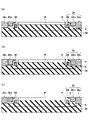
かかる構成のエッジリング38を有する処理容器10内においてパーティクルが溜まりやすい箇所を見つけるための実験を行った。一実施形態と比較例に係るパーティクルの状態の一例を示す図3を参照して、その結果について説明する。
これに対して、一実施形態にかかるクリーニング1について説明する。クリーニング1では、まず、静電チャック36の電極36aに直流電圧を印加した。そして、中央エッジリング38mを上下に移動させた。この結果、図3(a)にてパーティクルが溜まりやすいとされた箇所のすべて、すなわち、ウェハWの外周側壁及びウェハWの下の静電チャック36の側壁、内側エッジリング38iの表面全体と、中央エッジリング38mの裏面側のすべてにおいて、図3(c)のAに示すようにパーティクルを除去できた。
次に、一実施形態にかかるクリーニング2について説明する。クリーニング2では、まず、中央エッジリング38mの下部にクリーニングガスを供給した。そして、中央エッジリング38mを上下に移動させた。この結果、図3(a)にてパーティクルが溜まりやすいとされた箇所のすべての面において、図3(c)に示すようにパーティクルを除去できた。
最後に、一実施形態に係る実施形態にかかるクリーニング3について説明する。一実施形態に係る実施形態にかかるクリーニング3は、一実施形態にかかるクリーニング1とクリーニング2とを組み合わせたクリーニング方法である。
最後に、一実施形態にかかるクリーニング1~3の方法を使用したクリーニング処理及びウェハ処理の一例について、図4~図6を参照して説明する。図4は、一実施形態に係るクリーニング1のクリーニング処理及びウェハ処理の一例を示すフローチャートである。図5は、一実施形態に係るクリーニング2のクリーニング処理及びウェハ処理の一例を示すフローチャートである。図6は、一実施形態に係るクリーニング3のクリーニング処理及びウェハ処理の一例を示すフローチャートである。図4~図6の各処理は、制御部74により制御される。図4~図6の各処理が開始されるタイミングは、ウェハレスドライクリーニング(WLDC)終了後、又は、ロット間、又は、ウェハW毎であってもよい。
まず、クリーニング1のクリーニング処理及びウェハ処理について説明する。図4の処理が開始されると、制御部74は、処理容器10内を真空排気する(ステップS10)。次に、制御部74は、中央エッジリング38mの上下の移動を開始する(ステップS12)。次に、制御部74は、静電チャック36の電極36aに対して直流電圧(HV)の印加を開始する(ステップS14)。
次に、クリーニング2のクリーニング処理及びウェハ処理について説明する。図5の処理が開始されると、制御部74は、処理容器10内を真空排気する(ステップS10)。次に、制御部74は、中央エッジリング38mの上下の移動を開始する(ステップS12)。次に、制御部74は、N2ガスの導入を開始する(ステップS30)。次に、制御部74は、排気装置26を用いてN2ガスをパージする(ステップS32)。
次に、クリーニング3のクリーニング処理及びウェハ処理について説明する。図6の処理が開始されると、制御部74は、処理容器10内を真空排気する(ステップS10)。次に、制御部74は、中央エッジリング38mの上下の移動を開始する(ステップS12)。次に、制御部74は、静電チャック36の電極36aに直流電圧(HV)の印加を開始する(ステップS14)。次に、制御部74は、N2ガスの導入を開始する(ステップS30)。次に、制御部74は、排気装置26を用いてN2ガスをパージする(ステップS32)。
10:処理容器
12:載置台
20:バッフル板
26:排気装置
30:第2の高周波電源
36:静電チャック
38:エッジリング
38i:内側エッジリング
38m:中央エッジリング
38m1:環状部
38m2:タブ部
38o:外側エッジリング
40:直流電源
44:冷媒流路
51:シャワーヘッド
57:第1の高周波電源
66:ガス供給源
74:制御部
100:ハウジング
101:ピエゾアクチュエータ
102:リフトピン
103:連結部
105:軸受部
200:移動機構
Claims (13)
- 処理室内の静電チャックに載置された基板の近傍に設けられる内側エッジリングと、
前記内側エッジリングの外側に設けられ、移動機構により上下に移動が可能な中央エッジリングと、
前記中央エッジリングの外側に設けられる外側エッジリングとを有するエッジリングのクリーニング方法であって、
前記静電チャックに直流電圧を印加する工程と、
前記中央エッジリングを上又は下の少なくともいずれかに移動させる工程と、
を有するクリーニング方法。 - 処理室内の載置台に載置された基板の近傍に設けられる内側エッジリングと、
前記内側エッジリングの外側に設けられ、移動機構により上下に移動が可能な中央エッジリングと、
前記中央エッジリングの外側に設けられる外側エッジリングとを有するエッジリングのクリーニング方法であって、
前記中央エッジリングの下部にクリーニングガスを供給する工程と、
前記クリーニングガスが供給された状態で、前記中央エッジリングを上下動させる工程と、
を有するクリーニング方法。 - 前記内側エッジリングは、前記処理室内の静電チャックに載置された基板の近傍に設けられ、
前記静電チャックに直流電圧を印加する工程と、
前記中央エッジリングの下部にクリーニングガスを供給する工程と、
前記中央エッジリングを上又は下の少なくともいずれかに移動させる工程と、
を有する請求項1又は2に記載のクリーニング方法。 - 前記クリーニングガスは不活性ガスである、
請求項2又は3のいずれか一項に記載のクリーニング方法。 - 前記直流電圧を印加する工程において、前記静電チャックにプラスの電圧とマイナスの電圧とを交互に印加する、
請求項1に記載のクリーニング方法。 - 前記直流電圧を印加する工程において、前記中央エッジリングに付着した付着物の種類によって、印加する前記直流電圧の極性を制御する、
請求項1又は5に記載のクリーニング方法。 - 前記内側エッジリング及び/又は前記外側エッジリングは電極を備え、前記電極に直流電圧を印加する工程をさらに有する、
請求項1~6のいずれか一項に記載のクリーニング方法。 - 前記内側エッジリング及び/又は前記外側エッジリングは電極を備え、前記基板に対向する位置に設けられるシャワーヘッドと、前記電極とのいずれか1つ以上に直流電圧を印加する工程をさらに有する、
請求項1~7のいずれか一項に記載のクリーニング方法。 - 前記内側エッジリング及び/又は前記外側エッジリングは上下に移動可能であり、
前記内側エッジリング及び/又は前記外側エッジリングを上又は下の少なくともいずれかに移動させる工程をさらに有する、
請求項1~8のいずれか一項に記載のクリーニング方法。 - 前記直流電圧を印加する工程の後、前記直流電圧の印加を開始してから所定時間経過したかを判定する工程をさらに有する、
請求項1、5及び6のいずれか一項に記載のクリーニング方法。 - 前記クリーニングガスをパージする工程をさらに有する、
請求項2~4のいずれか一項に記載のクリーニング方法。 - 前記クリーニングガスを供給する工程の後、前記クリーニングガスの供給を開始してから所定時間経過したかを判定する工程をさらに有する、
請求項2~4及び11のいずれか一項に記載のクリーニング方法。 - 処理室内の静電チャックに載置された基板の近傍に設けられる内側エッジリングと、
前記内側エッジリングの外側に設けられ、移動機構により上下に移動が可能な中央エッジリングと、
前記中央エッジリングの外側に設けられる外側エッジリングとを有するエッジリングと、
制御部とを有する基板処理装置であって、
前記制御部は、
前記基板をプラズマ処理する工程と、
前記エッジリングをクリーニングする工程と、
を含み、
前記クリーニングする工程は、
前記静電チャックに直流電圧を印加する工程と、
前記中央エッジリングを上又は下の少なくともいずれかに移動させる工程と、
を含む、処理を制御する、基板処理装置。
Priority Applications (5)
| Application Number | Priority Date | Filing Date | Title |
|---|---|---|---|
| JP2018093308A JP7122864B2 (ja) | 2018-05-14 | 2018-05-14 | クリーニング方法及び基板処理装置 |
| TW108115809A TWI840355B (zh) | 2018-05-14 | 2019-05-08 | 清洗方法及基板處理裝置 |
| US16/409,441 US11264260B2 (en) | 2018-05-14 | 2019-05-10 | Cleaning method and substrate processing apparatus |
| KR1020190055473A KR102653085B1 (ko) | 2018-05-14 | 2019-05-13 | 클리닝 방법 및 기판 처리 장치 |
| US17/586,333 US20220148902A1 (en) | 2018-05-14 | 2022-01-27 | Cleaning method and substrate processing apparatus |
Applications Claiming Priority (1)
| Application Number | Priority Date | Filing Date | Title |
|---|---|---|---|
| JP2018093308A JP7122864B2 (ja) | 2018-05-14 | 2018-05-14 | クリーニング方法及び基板処理装置 |
Publications (3)
| Publication Number | Publication Date |
|---|---|
| JP2019201047A JP2019201047A (ja) | 2019-11-21 |
| JP2019201047A5 JP2019201047A5 (ja) | 2021-06-17 |
| JP7122864B2 true JP7122864B2 (ja) | 2022-08-22 |
Family
ID=68464165
Family Applications (1)
| Application Number | Title | Priority Date | Filing Date |
|---|---|---|---|
| JP2018093308A Active JP7122864B2 (ja) | 2018-05-14 | 2018-05-14 | クリーニング方法及び基板処理装置 |
Country Status (3)
| Country | Link |
|---|---|
| US (2) | US11264260B2 (ja) |
| JP (1) | JP7122864B2 (ja) |
| KR (1) | KR102653085B1 (ja) |
Families Citing this family (10)
| Publication number | Priority date | Publication date | Assignee | Title |
|---|---|---|---|---|
| WO2018219509A1 (en) * | 2017-06-01 | 2018-12-06 | Asml Netherlands B.V. | Particle removal apparatus and associated system |
| JP7370259B2 (ja) * | 2020-01-27 | 2023-10-27 | 東京エレクトロン株式会社 | 基板処理装置 |
| CN111341719B (zh) * | 2020-03-18 | 2023-04-14 | 北京北方华创微电子装备有限公司 | 承载装置、半导体设备及残余电荷的检测方法 |
| JP7409976B2 (ja) * | 2020-06-22 | 2024-01-09 | 東京エレクトロン株式会社 | プラズマ処理システム、プラズマ処理装置及びエッジリングの交換方法 |
| JP7455012B2 (ja) * | 2020-07-07 | 2024-03-25 | 東京エレクトロン株式会社 | プラズマ処理装置およびプラズマ処理装置の載置台 |
| KR102522687B1 (ko) * | 2020-10-20 | 2023-04-18 | 에이피시스템 주식회사 | 박막 제조 장치 |
| KR20220104955A (ko) * | 2021-01-19 | 2022-07-26 | 에스케이하이닉스 주식회사 | 중간 전극을 가진 기판 처리 장치 |
| JP2022181831A (ja) | 2021-05-27 | 2022-12-08 | 東京エレクトロン株式会社 | クリーニングを制御する方法及びプラズマ処理装置 |
| CN113430504B (zh) * | 2021-08-26 | 2021-11-09 | 上海陛通半导体能源科技股份有限公司 | 一种晶圆便捷升降夹紧的化学气相沉积设备 |
| WO2023120679A1 (ja) * | 2021-12-23 | 2023-06-29 | 東京エレクトロン株式会社 | プラズマ処理装置 |
Citations (3)
| Publication number | Priority date | Publication date | Assignee | Title |
|---|---|---|---|---|
| JP2012146743A (ja) | 2011-01-07 | 2012-08-02 | Tokyo Electron Ltd | 基板処理装置 |
| JP2012222235A (ja) | 2011-04-12 | 2012-11-12 | Hitachi High-Technologies Corp | プラズマ処理装置 |
| JP2016146472A (ja) | 2015-01-16 | 2016-08-12 | ラム リサーチ コーポレーションLam Research Corporation | 半導体ウエハ処理中におけるエッジ処理制御のための可動式エッジ連結リング |
Family Cites Families (6)
| Publication number | Priority date | Publication date | Assignee | Title |
|---|---|---|---|---|
| US5507874A (en) * | 1994-06-03 | 1996-04-16 | Applied Materials, Inc. | Method of cleaning of an electrostatic chuck in plasma reactors |
| US6475336B1 (en) * | 2000-10-06 | 2002-11-05 | Lam Research Corporation | Electrostatically clamped edge ring for plasma processing |
| JP4330467B2 (ja) | 2004-02-26 | 2009-09-16 | 東京エレクトロン株式会社 | プロセス装置及び該プロセス装置内のパーティクル除去方法 |
| JP5317424B2 (ja) | 2007-03-28 | 2013-10-16 | 東京エレクトロン株式会社 | プラズマ処理装置 |
| KR20110080811A (ko) * | 2010-01-07 | 2011-07-13 | 세메스 주식회사 | 정전척 유닛 및 이를 갖는 기판 처리 장치 |
| JP5976377B2 (ja) * | 2012-04-25 | 2016-08-23 | 東京エレクトロン株式会社 | 被処理基体に対する微粒子付着の制御方法、及び、処理装置 |
-
2018
- 2018-05-14 JP JP2018093308A patent/JP7122864B2/ja active Active
-
2019
- 2019-05-10 US US16/409,441 patent/US11264260B2/en active Active
- 2019-05-13 KR KR1020190055473A patent/KR102653085B1/ko active IP Right Grant
-
2022
- 2022-01-27 US US17/586,333 patent/US20220148902A1/en active Pending
Patent Citations (3)
| Publication number | Priority date | Publication date | Assignee | Title |
|---|---|---|---|---|
| JP2012146743A (ja) | 2011-01-07 | 2012-08-02 | Tokyo Electron Ltd | 基板処理装置 |
| JP2012222235A (ja) | 2011-04-12 | 2012-11-12 | Hitachi High-Technologies Corp | プラズマ処理装置 |
| JP2016146472A (ja) | 2015-01-16 | 2016-08-12 | ラム リサーチ コーポレーションLam Research Corporation | 半導体ウエハ処理中におけるエッジ処理制御のための可動式エッジ連結リング |
Also Published As
| Publication number | Publication date |
|---|---|
| JP2019201047A (ja) | 2019-11-21 |
| KR102653085B1 (ko) | 2024-03-29 |
| KR20190130501A (ko) | 2019-11-22 |
| US11264260B2 (en) | 2022-03-01 |
| US20220148902A1 (en) | 2022-05-12 |
| US20190348315A1 (en) | 2019-11-14 |
| TW202031376A (zh) | 2020-09-01 |
Similar Documents
| Publication | Publication Date | Title |
|---|---|---|
| JP7122864B2 (ja) | クリーニング方法及び基板処理装置 | |
| CN108630514B (zh) | 基板处理装置 | |
| JP7061918B2 (ja) | プラズマエッチング方法及びプラズマ処理装置 | |
| JP6995008B2 (ja) | 基板処理装置 | |
| KR102488217B1 (ko) | 기판 처리 장치 | |
| KR102434559B1 (ko) | 탑재대 및 플라즈마 처리 장치 | |
| JP5371238B2 (ja) | プラズマ処理装置およびプラズマ処理方法 | |
| JP4790458B2 (ja) | プラズマ処理装置 | |
| JP2011035266A (ja) | プラズマ処理装置及びプラズマ処理方法 | |
| JP7138418B2 (ja) | 脱離制御方法及びプラズマ処理装置 | |
| JP2022140585A (ja) | 基板処理装置 | |
| US20080242086A1 (en) | Plasma processing method and plasma processing apparatus | |
| JP2019176031A (ja) | プラズマ処理装置、及び被処理体の搬送方法 | |
| EP1944800A2 (en) | Method for manufacturing substrate mounting table | |
| KR20150001664A (ko) | 온도 제어 방법 및 플라즈마 처리 장치 | |
| KR102264005B1 (ko) | 플라즈마 처리 장치 | |
| TW201940257A (zh) | 清潔方法及處理裝置 | |
| JP2007042744A (ja) | プラズマ処理装置 | |
| TW201943014A (zh) | 被處理體的載置裝置及處理裝置 | |
| JP7204564B2 (ja) | プラズマ処理装置 | |
| US11587820B2 (en) | Mounting table, substrate processing apparatus, and control method | |
| TWI831956B (zh) | 清潔處理方法及電漿處理裝置 | |
| KR20170134812A (ko) | 기판 처리 장치 및 방법 | |
| TW202412559A (zh) | 用於處理基板之設備及用於處理基板之方法 | |
| KR100733080B1 (ko) | 식각장치 |
Legal Events
| Date | Code | Title | Description |
|---|---|---|---|
| A521 | Request for written amendment filed |
Free format text: JAPANESE INTERMEDIATE CODE: A523 Effective date: 20210430 |
|
| A621 | Written request for application examination |
Free format text: JAPANESE INTERMEDIATE CODE: A621 Effective date: 20210430 |
|
| A977 | Report on retrieval |
Free format text: JAPANESE INTERMEDIATE CODE: A971007 Effective date: 20220224 |
|
| A131 | Notification of reasons for refusal |
Free format text: JAPANESE INTERMEDIATE CODE: A131 Effective date: 20220301 |
|
| A521 | Request for written amendment filed |
Free format text: JAPANESE INTERMEDIATE CODE: A523 Effective date: 20220426 |
|
| TRDD | Decision of grant or rejection written | ||
| A01 | Written decision to grant a patent or to grant a registration (utility model) |
Free format text: JAPANESE INTERMEDIATE CODE: A01 Effective date: 20220712 |
|
| A61 | First payment of annual fees (during grant procedure) |
Free format text: JAPANESE INTERMEDIATE CODE: A61 Effective date: 20220809 |
|
| R150 | Certificate of patent or registration of utility model |
Ref document number: 7122864 Country of ref document: JP Free format text: JAPANESE INTERMEDIATE CODE: R150 |