JP7021063B2 - 半導体装置 - Google Patents
半導体装置 Download PDFInfo
- Publication number
- JP7021063B2 JP7021063B2 JP2018230703A JP2018230703A JP7021063B2 JP 7021063 B2 JP7021063 B2 JP 7021063B2 JP 2018230703 A JP2018230703 A JP 2018230703A JP 2018230703 A JP2018230703 A JP 2018230703A JP 7021063 B2 JP7021063 B2 JP 7021063B2
- Authority
- JP
- Japan
- Prior art keywords
- electrode
- region
- semiconductor device
- crystal member
- semiconductor
- Prior art date
- Legal status (The legal status is an assumption and is not a legal conclusion. Google has not performed a legal analysis and makes no representation as to the accuracy of the status listed.)
- Active
Links
- 239000004065 semiconductor Substances 0.000 title claims description 192
- 239000013078 crystal Substances 0.000 claims description 147
- 239000012535 impurity Substances 0.000 claims description 35
- 239000000758 substrate Substances 0.000 claims description 32
- 229910010271 silicon carbide Inorganic materials 0.000 claims description 30
- 229910052984 zinc sulfide Inorganic materials 0.000 claims description 27
- 230000010287 polarization Effects 0.000 claims description 19
- HBMJWWWQQXIZIP-UHFFFAOYSA-N silicon carbide Chemical compound [Si+]#[C-] HBMJWWWQQXIZIP-UHFFFAOYSA-N 0.000 claims description 16
- XUIMIQQOPSSXEZ-UHFFFAOYSA-N Silicon Chemical compound [Si] XUIMIQQOPSSXEZ-UHFFFAOYSA-N 0.000 claims description 11
- 229910052710 silicon Inorganic materials 0.000 claims description 11
- 239000010703 silicon Substances 0.000 claims description 11
- OKTJSMMVPCPJKN-UHFFFAOYSA-N Carbon Chemical compound [C] OKTJSMMVPCPJKN-UHFFFAOYSA-N 0.000 claims description 10
- 229910052799 carbon Inorganic materials 0.000 claims description 10
- 229910052732 germanium Inorganic materials 0.000 claims description 10
- GNPVGFCGXDBREM-UHFFFAOYSA-N germanium atom Chemical compound [Ge] GNPVGFCGXDBREM-UHFFFAOYSA-N 0.000 claims description 10
- 230000005533 two-dimensional electron gas Effects 0.000 description 6
- 239000004020 conductor Substances 0.000 description 5
- 239000000463 material Substances 0.000 description 4
- 238000000034 method Methods 0.000 description 4
- 238000004088 simulation Methods 0.000 description 3
- 238000010586 diagram Methods 0.000 description 2
- 229910002704 AlGaN Inorganic materials 0.000 description 1
- 229910013641 LiNbO 3 Inorganic materials 0.000 description 1
- 229910052782 aluminium Inorganic materials 0.000 description 1
- 239000000969 carrier Substances 0.000 description 1
- 230000000295 complement effect Effects 0.000 description 1
- 230000000694 effects Effects 0.000 description 1
- 229910052737 gold Inorganic materials 0.000 description 1
- 150000004820 halides Chemical class 0.000 description 1
- 230000017525 heat dissipation Effects 0.000 description 1
- 239000004047 hole gas Substances 0.000 description 1
- 238000004519 manufacturing process Methods 0.000 description 1
- 239000002184 metal Substances 0.000 description 1
- 229910052751 metal Inorganic materials 0.000 description 1
- 238000002488 metal-organic chemical vapour deposition Methods 0.000 description 1
- 238000001451 molecular beam epitaxy Methods 0.000 description 1
- 229910052759 nickel Inorganic materials 0.000 description 1
- 238000004549 pulsed laser deposition Methods 0.000 description 1
- 238000003892 spreading Methods 0.000 description 1
- 238000004544 sputter deposition Methods 0.000 description 1
- 229910052719 titanium Inorganic materials 0.000 description 1
- 239000012808 vapor phase Substances 0.000 description 1
- 238000001947 vapour-phase growth Methods 0.000 description 1
Images


Classifications
-
- H—ELECTRICITY
- H01—ELECTRIC ELEMENTS
- H01L—SEMICONDUCTOR DEVICES NOT COVERED BY CLASS H10
- H01L29/00—Semiconductor devices adapted for rectifying, amplifying, oscillating or switching, or capacitors or resistors with at least one potential-jump barrier or surface barrier, e.g. PN junction depletion layer or carrier concentration layer; Details of semiconductor bodies or of electrodes thereof ; Multistep manufacturing processes therefor
- H01L29/66—Types of semiconductor device ; Multistep manufacturing processes therefor
- H01L29/68—Types of semiconductor device ; Multistep manufacturing processes therefor controllable by only the electric current supplied, or only the electric potential applied, to an electrode which does not carry the current to be rectified, amplified or switched
- H01L29/76—Unipolar devices, e.g. field effect transistors
- H01L29/772—Field effect transistors
- H01L29/778—Field effect transistors with two-dimensional charge carrier gas channel, e.g. HEMT ; with two-dimensional charge-carrier layer formed at a heterojunction interface
- H01L29/7789—Field effect transistors with two-dimensional charge carrier gas channel, e.g. HEMT ; with two-dimensional charge-carrier layer formed at a heterojunction interface the two-dimensional charge carrier gas being at least partially not parallel to a main surface of the semiconductor body
-
- H—ELECTRICITY
- H01—ELECTRIC ELEMENTS
- H01L—SEMICONDUCTOR DEVICES NOT COVERED BY CLASS H10
- H01L29/00—Semiconductor devices adapted for rectifying, amplifying, oscillating or switching, or capacitors or resistors with at least one potential-jump barrier or surface barrier, e.g. PN junction depletion layer or carrier concentration layer; Details of semiconductor bodies or of electrodes thereof ; Multistep manufacturing processes therefor
- H01L29/02—Semiconductor bodies ; Multistep manufacturing processes therefor
- H01L29/04—Semiconductor bodies ; Multistep manufacturing processes therefor characterised by their crystalline structure, e.g. polycrystalline, cubic or particular orientation of crystalline planes
- H01L29/045—Semiconductor bodies ; Multistep manufacturing processes therefor characterised by their crystalline structure, e.g. polycrystalline, cubic or particular orientation of crystalline planes by their particular orientation of crystalline planes
-
- H—ELECTRICITY
- H01—ELECTRIC ELEMENTS
- H01L—SEMICONDUCTOR DEVICES NOT COVERED BY CLASS H10
- H01L29/00—Semiconductor devices adapted for rectifying, amplifying, oscillating or switching, or capacitors or resistors with at least one potential-jump barrier or surface barrier, e.g. PN junction depletion layer or carrier concentration layer; Details of semiconductor bodies or of electrodes thereof ; Multistep manufacturing processes therefor
- H01L29/02—Semiconductor bodies ; Multistep manufacturing processes therefor
- H01L29/12—Semiconductor bodies ; Multistep manufacturing processes therefor characterised by the materials of which they are formed
- H01L29/16—Semiconductor bodies ; Multistep manufacturing processes therefor characterised by the materials of which they are formed including, apart from doping materials or other impurities, only elements of Group IV of the Periodic System
- H01L29/1608—Silicon carbide
-
- H—ELECTRICITY
- H01—ELECTRIC ELEMENTS
- H01L—SEMICONDUCTOR DEVICES NOT COVERED BY CLASS H10
- H01L29/00—Semiconductor devices adapted for rectifying, amplifying, oscillating or switching, or capacitors or resistors with at least one potential-jump barrier or surface barrier, e.g. PN junction depletion layer or carrier concentration layer; Details of semiconductor bodies or of electrodes thereof ; Multistep manufacturing processes therefor
- H01L29/02—Semiconductor bodies ; Multistep manufacturing processes therefor
- H01L29/12—Semiconductor bodies ; Multistep manufacturing processes therefor characterised by the materials of which they are formed
- H01L29/16—Semiconductor bodies ; Multistep manufacturing processes therefor characterised by the materials of which they are formed including, apart from doping materials or other impurities, only elements of Group IV of the Periodic System
- H01L29/161—Semiconductor bodies ; Multistep manufacturing processes therefor characterised by the materials of which they are formed including, apart from doping materials or other impurities, only elements of Group IV of the Periodic System including two or more of the elements provided for in group H01L29/16, e.g. alloys
- H01L29/165—Semiconductor bodies ; Multistep manufacturing processes therefor characterised by the materials of which they are formed including, apart from doping materials or other impurities, only elements of Group IV of the Periodic System including two or more of the elements provided for in group H01L29/16, e.g. alloys in different semiconductor regions, e.g. heterojunctions
-
- H—ELECTRICITY
- H01—ELECTRIC ELEMENTS
- H01L—SEMICONDUCTOR DEVICES NOT COVERED BY CLASS H10
- H01L29/00—Semiconductor devices adapted for rectifying, amplifying, oscillating or switching, or capacitors or resistors with at least one potential-jump barrier or surface barrier, e.g. PN junction depletion layer or carrier concentration layer; Details of semiconductor bodies or of electrodes thereof ; Multistep manufacturing processes therefor
- H01L29/02—Semiconductor bodies ; Multistep manufacturing processes therefor
- H01L29/12—Semiconductor bodies ; Multistep manufacturing processes therefor characterised by the materials of which they are formed
- H01L29/26—Semiconductor bodies ; Multistep manufacturing processes therefor characterised by the materials of which they are formed including, apart from doping materials or other impurities, elements provided for in two or more of the groups H01L29/16, H01L29/18, H01L29/20, H01L29/22, H01L29/24, e.g. alloys
- H01L29/267—Semiconductor bodies ; Multistep manufacturing processes therefor characterised by the materials of which they are formed including, apart from doping materials or other impurities, elements provided for in two or more of the groups H01L29/16, H01L29/18, H01L29/20, H01L29/22, H01L29/24, e.g. alloys in different semiconductor regions, e.g. heterojunctions
-
- H—ELECTRICITY
- H01—ELECTRIC ELEMENTS
- H01L—SEMICONDUCTOR DEVICES NOT COVERED BY CLASS H10
- H01L29/00—Semiconductor devices adapted for rectifying, amplifying, oscillating or switching, or capacitors or resistors with at least one potential-jump barrier or surface barrier, e.g. PN junction depletion layer or carrier concentration layer; Details of semiconductor bodies or of electrodes thereof ; Multistep manufacturing processes therefor
- H01L29/66—Types of semiconductor device ; Multistep manufacturing processes therefor
- H01L29/66007—Multistep manufacturing processes
- H01L29/66075—Multistep manufacturing processes of devices having semiconductor bodies comprising group 14 or group 13/15 materials
- H01L29/66227—Multistep manufacturing processes of devices having semiconductor bodies comprising group 14 or group 13/15 materials the devices being controllable only by the electric current supplied or the electric potential applied, to an electrode which does not carry the current to be rectified, amplified or switched, e.g. three-terminal devices
- H01L29/66409—Unipolar field-effect transistors
- H01L29/66431—Unipolar field-effect transistors with a heterojunction interface channel or gate, e.g. HFET, HIGFET, SISFET, HJFET, HEMT
-
- H—ELECTRICITY
- H01—ELECTRIC ELEMENTS
- H01L—SEMICONDUCTOR DEVICES NOT COVERED BY CLASS H10
- H01L29/00—Semiconductor devices adapted for rectifying, amplifying, oscillating or switching, or capacitors or resistors with at least one potential-jump barrier or surface barrier, e.g. PN junction depletion layer or carrier concentration layer; Details of semiconductor bodies or of electrodes thereof ; Multistep manufacturing processes therefor
- H01L29/66—Types of semiconductor device ; Multistep manufacturing processes therefor
- H01L29/66007—Multistep manufacturing processes
- H01L29/66075—Multistep manufacturing processes of devices having semiconductor bodies comprising group 14 or group 13/15 materials
- H01L29/66227—Multistep manufacturing processes of devices having semiconductor bodies comprising group 14 or group 13/15 materials the devices being controllable only by the electric current supplied or the electric potential applied, to an electrode which does not carry the current to be rectified, amplified or switched, e.g. three-terminal devices
- H01L29/66409—Unipolar field-effect transistors
- H01L29/66446—Unipolar field-effect transistors with an active layer made of a group 13/15 material, e.g. group 13/15 velocity modulation transistor [VMT], group 13/15 negative resistance FET [NERFET]
- H01L29/66462—Unipolar field-effect transistors with an active layer made of a group 13/15 material, e.g. group 13/15 velocity modulation transistor [VMT], group 13/15 negative resistance FET [NERFET] with a heterojunction interface channel or gate, e.g. HFET, HIGFET, SISFET, HJFET, HEMT
-
- H—ELECTRICITY
- H01—ELECTRIC ELEMENTS
- H01L—SEMICONDUCTOR DEVICES NOT COVERED BY CLASS H10
- H01L29/00—Semiconductor devices adapted for rectifying, amplifying, oscillating or switching, or capacitors or resistors with at least one potential-jump barrier or surface barrier, e.g. PN junction depletion layer or carrier concentration layer; Details of semiconductor bodies or of electrodes thereof ; Multistep manufacturing processes therefor
- H01L29/66—Types of semiconductor device ; Multistep manufacturing processes therefor
- H01L29/68—Types of semiconductor device ; Multistep manufacturing processes therefor controllable by only the electric current supplied, or only the electric potential applied, to an electrode which does not carry the current to be rectified, amplified or switched
- H01L29/76—Unipolar devices, e.g. field effect transistors
- H01L29/772—Field effect transistors
- H01L29/778—Field effect transistors with two-dimensional charge carrier gas channel, e.g. HEMT ; with two-dimensional charge-carrier layer formed at a heterojunction interface
- H01L29/7788—Vertical transistors
-
- H—ELECTRICITY
- H01—ELECTRIC ELEMENTS
- H01L—SEMICONDUCTOR DEVICES NOT COVERED BY CLASS H10
- H01L29/00—Semiconductor devices adapted for rectifying, amplifying, oscillating or switching, or capacitors or resistors with at least one potential-jump barrier or surface barrier, e.g. PN junction depletion layer or carrier concentration layer; Details of semiconductor bodies or of electrodes thereof ; Multistep manufacturing processes therefor
- H01L29/02—Semiconductor bodies ; Multistep manufacturing processes therefor
- H01L29/06—Semiconductor bodies ; Multistep manufacturing processes therefor characterised by their shape; characterised by the shapes, relative sizes, or dispositions of the semiconductor regions ; characterised by the concentration or distribution of impurities within semiconductor regions
- H01L29/0603—Semiconductor bodies ; Multistep manufacturing processes therefor characterised by their shape; characterised by the shapes, relative sizes, or dispositions of the semiconductor regions ; characterised by the concentration or distribution of impurities within semiconductor regions characterised by particular constructional design considerations, e.g. for preventing surface leakage, for controlling electric field concentration or for internal isolations regions
- H01L29/0642—Isolation within the component, i.e. internal isolation
- H01L29/0649—Dielectric regions, e.g. SiO2 regions, air gaps
-
- H—ELECTRICITY
- H01—ELECTRIC ELEMENTS
- H01L—SEMICONDUCTOR DEVICES NOT COVERED BY CLASS H10
- H01L29/00—Semiconductor devices adapted for rectifying, amplifying, oscillating or switching, or capacitors or resistors with at least one potential-jump barrier or surface barrier, e.g. PN junction depletion layer or carrier concentration layer; Details of semiconductor bodies or of electrodes thereof ; Multistep manufacturing processes therefor
- H01L29/40—Electrodes ; Multistep manufacturing processes therefor
- H01L29/41—Electrodes ; Multistep manufacturing processes therefor characterised by their shape, relative sizes or dispositions
- H01L29/423—Electrodes ; Multistep manufacturing processes therefor characterised by their shape, relative sizes or dispositions not carrying the current to be rectified, amplified or switched
- H01L29/42312—Gate electrodes for field effect devices
- H01L29/42316—Gate electrodes for field effect devices for field-effect transistors
Description
図面は模式的または概念的なものであり、各部分の厚さと幅との関係、部分間の大きさの比率などは、必ずしも現実のものと同一とは限らない。同じ部分を表す場合であっても、図面により互いの寸法や比率が異なって表される場合もある。
本願明細書と各図において、既出の図に関して前述したものと同様の要素には同一の符号を付して詳細な説明は適宜省略する。
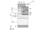
図1は、第1実施形態に係る半導体装置を例示する模式的断面図である。
図1に示すように、第1実施形態に係る半導体装置110は、第1電極51、第2電極52、第3電極53、半導体部材10及び第1結晶部材21を含む。
図2は、半導体装置110のオン時における電子密度のシミュレーション結果を例示している。図2において、画像の明暗は、電子密度の高低に対応する。画像が暗い部分における電子密度は、画像が明るい部分における電子密度よりも高い。図2に示すように、電子密度は、第1部分領域11aと第3電極53との間の領域において高い。電子密度の高い領域は、第2部分領域11bで広がり、第3電極53の下側に広がっている。実施形態においては、第2部分領域11bにより、電子密度が高い領域が得られる。実施形態においては、第2部分領域11bが設けられない場合に比べて、オン抵抗を低くできる。
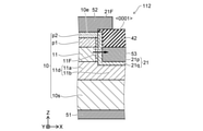
以下、実施形態に係る半導体装置111について、半導体装置110とは異なる部分について説明する。半導体装置111においても、例えば、第1結晶部材21は、ウルツ鉱構造を有する。半導体装置111においては、第1結晶部材21の<000-1>方向は、第1領域11から第3電極53への向きの成分を有する。このとき、半導体部材10のうちの第3電極53の近傍領域に、キャリア領域として、2次元ホールガス10hが生じる。半導体装置111においても、第2部分領域11bが設けられることにより、オン抵抗を低くできる。特性の向上が可能な半導体装置を提供できる。
以下、実施形態に係る半導体装置112について、半導体装置110とは異なる部分について説明する。半導体装置112においては、第1絶縁部材41が設けられていない。半導体装置112においては、第1結晶部材21は、複数の領域(領域21p及び領域21q)を含む。領域21pは、第2方向(X軸方向)において、第1領域11と第3電極53との間にある。領域21qは、第1方向(Z軸方向)において、第2部分領域11bと第3電極53との間にある。領域21qは、第2部分領域11bと第3電極53とを電気的に絶縁する。
以下、実施形態に係る半導体装置113について、半導体装置111とは異なる部分について説明する。半導体装置113においても、第1絶縁部材41が設けられていない。半導体装置113においても、第1結晶部材21は、領域21p及び領域21qを含む。領域21pは、第2方向において、第1領域11と第3電極53との間にある。領域21qは、第1方向において、第2部分領域11bと第3電極53との間にある。領域21qは、第2部分領域11bと第3電極53とを電気的に絶縁する。
図6は、第2実施形態に係る半導体装置を例示する模式的断面図である。
図6に示すように、第2実施形態に係る半導体装置120は、第1電極51、第2電極52、第3電極53、第4電極54、第5電極55、半導体部材10、第1結晶部材21及び第2結晶部材22を含む。
以下、実施形態に係る半導体装置121について、半導体装置120とは異なる部分について説明する。半導体装置121においても、第1結晶部材21は、ウルツ鉱構造を有する。半導体装置121においては、第1結晶部材21の<000-1>方向は、第1領域11から第3電極53への向きの成分を有する。第2結晶部材22の<000-1>方向は、第2領域12から第5電極55への向きの成分を有する。このとき、半導体部材10のうちの第3電極53の近傍領域、及び、第5電極55の近傍領域に、キャリア領域として、2次元ホールガス10hが生じる。半導体装置121においても、オン抵抗を低くできる。半導体装置121において、第2部分領域11b及び第4部分領域12dが設けられることにより、オン抵抗をさらに低くできる。特性の向上が可能な半導体装置を提供できる。
図8の横軸は、ゲート電圧Vg(V)である。ゲート電圧Vgは、第2電極52(ソース電極)を規準にしたときの第3電極53(ゲート電極)の電位に対応する。図8の縦軸は、ドレイン電流Id(×10-6A)である。図8には、距離dxが0nm、150nm、300nmまたは400nmのときの結果が例示されている。この例では、第3電極53のX軸方向の長さは、800nmである。図8から分かるように、距離dxが長くなると、同じゲート電圧Vgにおけるドレイン電流Idが大きくなる。
図9の横軸は、ゲート電圧Vg(V)である。図9の縦軸は、ドレイン電流Id(×10-5A)である。図9には、第1領域11におけるp形の不純物濃度Cpが、5×1017cm-3、7×1017cm-3、8×1017cm-3、または、9×1017cm-3のときの特性が例示されている。図9から分かるように、不純物濃度が低いと、ゲート電圧Vgが0Vのときのドレイン電流Id大きい。第1領域11における不純物濃度を制御することで、しきい値電圧を制御できる。半導体装置120の1つの例において、第1領域11におけるp形の不純物濃度Cpは、7×1017cm-3以上であることが好ましい。これにより、例えば、オフ電流を小さくできる。安定したノーマリオフ特性が得られる。
以下、実施形態に係る半導体装置122について、半導体装置120とは異なる部分について説明する。半導体装置122においては、第1絶縁部材41及び第3絶縁部材43が設けられていない。
以下、実施形態に係る半導体装置123について、半導体装置121とは異なる部分について説明する。半導体装置123においても、第1絶縁部材41及び第3絶縁部材43が設けられていない。半導体装置122においては、第1結晶部材21は、領域21p及び領域21qを含む。第2結晶部材22は、領域22p及び領域22qを含む。
図12は、第3実施形態に係る半導体装置を例示する模式的断面図である。
図12に示すように、第3実施形態に係る半導体装置130は、第1電極51、第2電極52、第3電極53、第4電極54、半導体部材10、第1結晶部材21及び第2結晶部材22を含む。
以下、実施形態に係る半導体装置131について、半導体装置130とは異なる部分について説明する。半導体装置131においては、第1絶縁部材41が設けられない。半導体装置131は、第1結晶部材21及び第2結晶部材22に、加えて、第3結晶部材23をさらに含む。
Claims (18)
- 第1電極と、
第2電極であって、前記第1電極から前記第2電極への方向は、第1方向に沿う、前記第2電極と、
第3電極であって、前記第3電極の前記第1方向における位置は、前記第1電極の前記第1方向における位置と、前記第2電極の前記第1方向における位置と、の間にある、前記第3電極と、
炭化シリコン、シリコン、カーボン及びゲルマニウムよりなる群から選択された少なくとも1つを含む半導体部材であって、前記半導体部材は、第1領域、第1部分領域及び第2部分領域を含み、前記第1領域は、前記第1方向において前記第1電極と前記第2電極との間にあり、前記第1領域から前記第3電極への第2方向は、前記第1方向と交差し、前記第1部分領域は、前記第1方向において前記第1電極と前記第1領域との間にあり、前記第1部分領域から前記第2部分領域への方向は、前記第2方向に沿い、前記第2部分領域は、前記第1方向において前記第1電極と前記第3電極との間にある、前記半導体部材と、
前記第2方向において、前記第1領域と前記第3電極との間に設けられた第1結晶部材と、
を備え、
前記第3電極に印加される電圧により、前記第1電極と前記第2電極との間に流れる電流が制御でき、
前記第1結晶部材は、ウルツ鉱構造を有し、
前記第1結晶部材の<0001>方向または<000-1>方向は、前記第2方向に沿う、半導体装置。 - 前記第1結晶部材は、AlxGa1-xN(0<x≦1)を含む、請求項1記載の半導体装置。
- 第1電極と、
第2電極であって、前記第1電極から前記第2電極への方向は、第1方向に沿う、前記第2電極と、
第3電極であって、前記第3電極の前記第1方向における位置は、前記第1電極の前記第1方向における位置と、前記第2電極の前記第1方向における位置と、の間にある、前記第3電極と、
炭化シリコン、シリコン、カーボン及びゲルマニウムよりなる群から選択された少なくとも1つを含む半導体部材であって、前記半導体部材は、第1領域、第1部分領域及び第2部分領域を含み、前記第1領域は、前記第1方向において前記第1電極と前記第2電極との間にあり、前記第1領域から前記第3電極への第2方向は、前記第1方向と交差し、前記第1部分領域は、前記第1方向において前記第1電極と前記第1領域との間にあり、前記第1部分領域から前記第2部分領域への方向は、前記第2方向に沿い、前記第2部分領域は、前記第1方向において前記第1電極と前記第3電極との間にある、前記半導体部材と、
前記第2方向において、前記第1領域と前記第3電極との間に設けられた第1結晶部材と、
を備え、
前記第3電極に印加される電圧により、前記第1電極と前記第2電極との間に流れる電流が制御でき、
前記第1結晶部材の分極の負から正への向き、または、前記分極の正から負への向きは、前記第2方向に沿う、半導体装置。 - 前記半導体部材は、前記第1電極と前記第1部分領域との間、及び、前記第1電極と前記第2部分領域との間に設けられた基板をさらに含む、請求項1記載の半導体装置。
- 第1電極と、
第2電極であって、前記第1電極から前記第2電極への方向は、第1方向に沿う、前記第2電極と、
第3電極であって、前記第3電極の前記第1方向における位置は、前記第1電極の前記第1方向における位置と、前記第2電極の前記第1方向における位置と、の間にある、前記第3電極と、
炭化シリコン、シリコン、カーボン及びゲルマニウムよりなる群から選択された少なくとも1つを含む半導体部材であって、前記半導体部材は、第1領域、第1部分領域及び第2部分領域を含み、前記第1領域は、前記第1方向において前記第1電極と前記第2電極との間にあり、前記第1領域から前記第3電極への第2方向は、前記第1方向と交差し、前記第1部分領域は、前記第1方向において前記第1電極と前記第1領域との間にあり、前記第1部分領域から前記第2部分領域への方向は、前記第2方向に沿い、前記第2部分領域は、前記第1方向において前記第1電極と前記第3電極との間にある、前記半導体部材と、
前記第2方向において、前記第1領域と前記第3電極との間に設けられた第1結晶部材と、
を備え、
前記第3電極に印加される電圧により、前記第1電極と前記第2電極との間に流れる電流が制御でき、
前記第1結晶部材は、ウルツ鉱構造を有し、
前記第1結晶部材の<0001>方向は、前記第1領域から前記第3電極への向きの成分を有し、
前記第1領域はp形である、半導体装置。 - 第1電極と、
第2電極であって、前記第1電極から前記第2電極への方向は、第1方向に沿う、前記第2電極と、
第3電極であって、前記第3電極の前記第1方向における位置は、前記第1電極の前記第1方向における位置と、前記第2電極の前記第1方向における位置と、の間にある、前記第3電極と、
炭化シリコン、シリコン、カーボン及びゲルマニウムよりなる群から選択された少なくとも1つを含む半導体部材であって、前記半導体部材は、第1領域、第1部分領域及び第2部分領域を含み、前記第1領域は、前記第1方向において前記第1電極と前記第2電極との間にあり、前記第1領域から前記第3電極への第2方向は、前記第1方向と交差し、前記第1部分領域は、前記第1方向において前記第1電極と前記第1領域との間にあり、前記第1部分領域から前記第2部分領域への方向は、前記第2方向に沿い、前記第2部分領域は、前記第1方向において前記第1電極と前記第3電極との間にある、前記半導体部材と、
前記第2方向において、前記第1領域と前記第3電極との間に設けられた第1結晶部材と、
を備え、
前記第3電極に印加される電圧により、前記第1電極と前記第2電極との間に流れる電流が制御でき、
前記第1結晶部材は、ウルツ鉱構造を有し、
前記第1結晶部材の<000-1>方向は、前記第1領域から前記第3電極への向きの成分を有し、
前記第1領域はn形である、半導体装置。 - 前記第2部分領域と前記第3電極との間に設けられた第1絶縁部材をさらに備えた請求項1~6のいずれか1つに記載の半導体装置。
- 前記第1結晶部材は、前記第1方向において前記第2部分領域と前記第3電極との間の領域を含む、請求項1~6のいずれか1つに記載の半導体装置。
- 前記第1方向において、前記第3電極と、前記第2電極の一部と、の間に設けられた第2絶縁部材をさらに備えた、請求項1~8のいずれか1つに記載の半導体装置。
- ドレイン電極と、
ソース電極であって、前記ドレイン電極から前記ソース電極への方向は、第1方向に沿う、前記ソース電極と、
ゲート電極であって、前記ゲート電極の前記第1方向における位置は、前記ドレイン電極の前記第1方向における位置と、前記ソース電極の前記第1方向における位置と、の間にある、前記ゲート電極と、
別のソース電極であって、前記ドレイン電極から前記別のソース電極への方向は、前記第1方向に沿い、前記ソース電極から前記別のソース電極への方向は、前記第1方向と交差する第2方向に沿う、前記別のソース電極と、
別のゲート電極であって、前記別のゲート電極の前記第1方向における位置は、前記ドレイン電極の前記第1方向における前記位置と、前記別のソース電極の前記第1方向における位置と、の間にあり、前記ゲート電極から前記別のゲート電極への方向は、前記第2方向に沿う、前記別のゲート電極と、
炭化シリコン、シリコン、カーボン及びゲルマニウムよりなる群から選択された少なくとも1つを含む半導体部材であって、前記半導体部材は、第1領域及び第2領域を含み、前記第1領域は、前記第1方向において前記ドレイン電極と前記ソース電極との間にあり、前記第2領域は、前記第1方向において前記ドレイン電極と前記別のソース電極との間にある、前記半導体部材と、
前記第2方向において、前記第1領域と前記ゲート電極との間に設けられた第1結晶部材と、
前記第2方向において、前記第2領域と前記別のゲート電極との間に設けられた第2結晶部材と、
を備えた半導体装置。 - 前記半導体部材は、前記ドレイン電極と前記第1領域との間、及び、前記ドレイン電極と前記第2領域との間に設けられた基板をさらに含む、請求項10記載の半導体装置。
- 前記半導体部材は、第1部分領域、第2部分領域、第3部分領域及び第4部分領域をさらに含み、
前記第1部分領域は、前記第1方向において、前記ドレイン電極と前記第1領域との間にあり、
前記第1部分領域から前記第2部分領域への方向は、前記第2方向に沿い、
前記第2部分領域は、前記第1方向において前記ドレイン電極と前記ゲート電極との間にあり、
前記第3部分領域は、前記第1方向において、前記ドレイン電極と前記第2領域との間にあり、
前記第3部分領域から前記第4部分領域への方向は、前記第2方向に沿い、
前記第4部分領域は、前記第1方向において前記ドレイン電極と前記別のゲート電極との間にある、請求項10または11に記載の半導体装置。 - 前記半導体部材は、第3領域をさらに含み、
前記第3領域は、前記第2方向において、前記ゲート電極と前記第2領域との間にあり、
前記第3領域における不純物濃度は、前記第2領域における不純物濃度よりも高い、
請求項10~12のいずれか1つに記載の半導体装置。 - 前記第1結晶部材及び前記第2結晶部材は、ウルツ鉱構造を有し、
前記第1結晶部材の<0001>方向または<000-1>方向は、前記第2方向に沿い、
前記第2結晶部材の<0001>方向または<000-1>方向は、前記第2方向に沿う、請求項10~13のいずれか1つに記載の半導体装置。 - 前記第1結晶部材及び前記第2結晶部材は、ウルツ鉱構造を有し、
前記第1結晶部材の<0001>方向は、前記第1領域から前記ゲート電極への向きの成分を有し、
前記第2結晶部材の<0001>方向は、前記第2領域から前記別のゲート電極への向きの成分を有し、
前記第1領域及び第2領域はp形である、請求項10~13のいずれか1つに記載の半導体装置。 - 前記第1結晶部材及び前記第2結晶部材は、ウルツ鉱構造を有し、
前記第1結晶部材の<000-1>方向は、前記第1領域から前記ゲート電極への向きの成分を有し、
前記第2結晶部材の<000-1>方向は、前記第2領域から前記別のゲート電極への向きの成分を有し、
前記第1領域及び第2領域はn形である、請求項10~13のいずれか1つに記載の半導体装置。 - 第1電極と、
第2電極と、
第3電極と、
第4電極であって、前記第3電極から前記第4電極への第1方向は、前記第1電極から前記第2電極への第2方向と交差し、前記第3電極の前記第2方向における位置は、前記第1電極の前記第2方向における位置と、前記第2電極の前記第2方向における位置と、の間にある、前記第4電極と、
炭化シリコン、シリコン、カーボン及びゲルマニウムよりなる群から選択された少なくとも1つを含む半導体部材であって、前記半導体部材は、第1領域及び第2領域を含み、前記第1領域は、前記第2方向において前記第1電極と前記第3電極との間にあり、前記第2領域は、前記第2方向において前記第3電極と前記第2電極との間にある、前記第1領域及び前記第2領域は、前記第4電極と電気的に接続された、前記半導体部材と、
前記第2方向において、前記第1領域と前記第3電極との間に設けられた第1結晶部材と、
前記第2方向において、前記第2領域と前記第3電極との間に設けられた第2結晶部材と、
を備え、
前記第3電極に印加される電圧により、前記第1電極と前記第2電極との間に流れる電流が制御でき、
前記第1領域及び前記第2領域は、前記第4電極と電気的に接続された半導体装置。 - 前記第1結晶部材及び前記第2結晶部材は、ウルツ鉱構造を有し、
前記第1結晶部材の<0001>方向は、前記第1領域から前記第3電極への向きの成分を有し、
前記第2結晶部材の<0001>方向は、前記第3電極から前記第2領域への向きの成分を有する、請求項17記載の半導体装置。
Priority Applications (2)
| Application Number | Priority Date | Filing Date | Title |
|---|---|---|---|
| JP2018230703A JP7021063B2 (ja) | 2018-12-10 | 2018-12-10 | 半導体装置 |
| US16/568,490 US11075262B2 (en) | 2018-12-10 | 2019-09-12 | Semiconductor device |
Applications Claiming Priority (1)
| Application Number | Priority Date | Filing Date | Title |
|---|---|---|---|
| JP2018230703A JP7021063B2 (ja) | 2018-12-10 | 2018-12-10 | 半導体装置 |
Publications (3)
| Publication Number | Publication Date |
|---|---|
| JP2020096003A JP2020096003A (ja) | 2020-06-18 |
| JP2020096003A5 JP2020096003A5 (ja) | 2021-02-18 |
| JP7021063B2 true JP7021063B2 (ja) | 2022-02-16 |
Family
ID=70970317
Family Applications (1)
| Application Number | Title | Priority Date | Filing Date |
|---|---|---|---|
| JP2018230703A Active JP7021063B2 (ja) | 2018-12-10 | 2018-12-10 | 半導体装置 |
Country Status (2)
| Country | Link |
|---|---|
| US (1) | US11075262B2 (ja) |
| JP (1) | JP7021063B2 (ja) |
Families Citing this family (2)
| Publication number | Priority date | Publication date | Assignee | Title |
|---|---|---|---|---|
| JP7021063B2 (ja) * | 2018-12-10 | 2022-02-16 | 株式会社東芝 | 半導体装置 |
| CN117317001A (zh) * | 2019-04-12 | 2023-12-29 | 广东致能科技有限公司 | 一种半导体器件及其制造方法 |
Citations (7)
| Publication number | Priority date | Publication date | Assignee | Title |
|---|---|---|---|---|
| JP2006086548A (ja) | 2005-12-12 | 2006-03-30 | Nissan Motor Co Ltd | 電界効果トランジスタ |
| JP2006344759A (ja) | 2005-06-08 | 2006-12-21 | Sharp Corp | トレンチ型mosfet及びその製造方法 |
| JP2009194065A (ja) | 2008-02-13 | 2009-08-27 | Denso Corp | 炭化珪素半導体装置およびその製造方法 |
| JP2015008331A (ja) | 2006-11-20 | 2015-01-15 | パナソニック株式会社 | 半導体装置 |
| US20150014700A1 (en) | 2013-07-15 | 2015-01-15 | Hrl Laboratories Llc | Vertical iii-nitride semiconductor device with a vertically formed two dimensional electron gas |
| JP2017220667A (ja) | 2016-05-24 | 2017-12-14 | インフィネオン テクノロジーズ アーゲーInfineon Technologies Ag | トレンチゲート構造を有するワイドバンドギャップ半導体素子 |
| JP2018010995A (ja) | 2016-07-14 | 2018-01-18 | 株式会社豊田中央研究所 | 炭化珪素半導体装置とその製造方法 |
Family Cites Families (9)
| Publication number | Priority date | Publication date | Assignee | Title |
|---|---|---|---|---|
| JP2007103727A (ja) | 2005-10-05 | 2007-04-19 | Toyota Motor Corp | 炭化珪素半導体装置及びその製造方法 |
| JP5207874B2 (ja) | 2008-08-08 | 2013-06-12 | 親夫 木村 | 半導体装置およびその製造方法 |
| JP2016058648A (ja) | 2014-09-11 | 2016-04-21 | 株式会社東芝 | 半導体装置 |
| US9601610B1 (en) * | 2015-06-18 | 2017-03-21 | Hrl Laboratories, Llc | Vertical super junction III/nitride HEMT with vertically formed two dimensional electron gas |
| CN106611781A (zh) * | 2015-10-27 | 2017-05-03 | 上海新昇半导体科技有限公司 | 量子阱器件及其形成方法 |
| WO2019188767A1 (ja) * | 2018-03-29 | 2019-10-03 | パナソニックIpマネジメント株式会社 | 半導体装置及びその製造方法 |
| JP6924166B2 (ja) | 2018-05-14 | 2021-08-25 | 株式会社東芝 | 半導体装置 |
| JP6903604B2 (ja) | 2018-05-14 | 2021-07-14 | 株式会社東芝 | 半導体装置 |
| JP7021063B2 (ja) * | 2018-12-10 | 2022-02-16 | 株式会社東芝 | 半導体装置 |
-
2018
- 2018-12-10 JP JP2018230703A patent/JP7021063B2/ja active Active
-
2019
- 2019-09-12 US US16/568,490 patent/US11075262B2/en active Active
Patent Citations (7)
| Publication number | Priority date | Publication date | Assignee | Title |
|---|---|---|---|---|
| JP2006344759A (ja) | 2005-06-08 | 2006-12-21 | Sharp Corp | トレンチ型mosfet及びその製造方法 |
| JP2006086548A (ja) | 2005-12-12 | 2006-03-30 | Nissan Motor Co Ltd | 電界効果トランジスタ |
| JP2015008331A (ja) | 2006-11-20 | 2015-01-15 | パナソニック株式会社 | 半導体装置 |
| JP2009194065A (ja) | 2008-02-13 | 2009-08-27 | Denso Corp | 炭化珪素半導体装置およびその製造方法 |
| US20150014700A1 (en) | 2013-07-15 | 2015-01-15 | Hrl Laboratories Llc | Vertical iii-nitride semiconductor device with a vertically formed two dimensional electron gas |
| JP2017220667A (ja) | 2016-05-24 | 2017-12-14 | インフィネオン テクノロジーズ アーゲーInfineon Technologies Ag | トレンチゲート構造を有するワイドバンドギャップ半導体素子 |
| JP2018010995A (ja) | 2016-07-14 | 2018-01-18 | 株式会社豊田中央研究所 | 炭化珪素半導体装置とその製造方法 |
Also Published As
| Publication number | Publication date |
|---|---|
| US20200185492A1 (en) | 2020-06-11 |
| US11075262B2 (en) | 2021-07-27 |
| JP2020096003A (ja) | 2020-06-18 |
Similar Documents
| Publication | Publication Date | Title |
|---|---|---|
| US8368121B2 (en) | Enhancement-mode HFET circuit arrangement having high power and high threshold voltage | |
| TWI531060B (zh) | 具有提昇之可靠性的高功率半導體電子元件 | |
| JP6442803B2 (ja) | エンハンスメントモードiii族窒化物デバイス | |
| JP4645313B2 (ja) | 半導体装置 | |
| JP5779704B2 (ja) | 半導体装置 | |
| US9099382B2 (en) | Enhancement mode III-nitride transistors | |
| JP4514063B2 (ja) | Ed型インバータ回路および集積回路素子 | |
| CN111554752B (zh) | 使用斜切衬底的高功率氮化镓电子器件 | |
| US7759760B2 (en) | Semiconductor switching element and semiconductor circuit apparatus | |
| JP5414709B2 (ja) | トランジスタ | |
| US20130292699A1 (en) | Nitride semiconductor device | |
| JP4917319B2 (ja) | トランジスタ | |
| JP2007035905A (ja) | 窒化物半導体素子 | |
| JP4938531B2 (ja) | 半導体装置 | |
| JP2005086171A (ja) | 半導体装置及びその製造方法 | |
| JP2007158143A (ja) | ヘテロ接合型電界効果トランジスタ | |
| US10910490B2 (en) | Semiconductor device | |
| JP2008016588A (ja) | GaN系半導体素子 | |
| JP7021063B2 (ja) | 半導体装置 | |
| US9391187B2 (en) | Semiconductor heterojunction device | |
| EP2360728B1 (en) | Enhancement mode III-nitride transistors with single gate dielectric structure | |
| JP6903604B2 (ja) | 半導体装置 | |
| JP2020077712A (ja) | 半導体装置 | |
| WO2023176373A1 (ja) | 半導体装置 | |
| US20220140125A1 (en) | Semiconductor device |
Legal Events
| Date | Code | Title | Description |
|---|---|---|---|
| A621 | Written request for application examination |
Free format text: JAPANESE INTERMEDIATE CODE: A621 Effective date: 20200904 |
|
| A521 | Request for written amendment filed |
Free format text: JAPANESE INTERMEDIATE CODE: A523 Effective date: 20210107 |
|
| A977 | Report on retrieval |
Free format text: JAPANESE INTERMEDIATE CODE: A971007 Effective date: 20210730 |
|
| A131 | Notification of reasons for refusal |
Free format text: JAPANESE INTERMEDIATE CODE: A131 Effective date: 20210803 |
|
| A521 | Request for written amendment filed |
Free format text: JAPANESE INTERMEDIATE CODE: A523 Effective date: 20211001 |
|
| TRDD | Decision of grant or rejection written | ||
| A01 | Written decision to grant a patent or to grant a registration (utility model) |
Free format text: JAPANESE INTERMEDIATE CODE: A01 Effective date: 20220105 |
|
| A61 | First payment of annual fees (during grant procedure) |
Free format text: JAPANESE INTERMEDIATE CODE: A61 Effective date: 20220203 |
|
| R151 | Written notification of patent or utility model registration |
Ref document number: 7021063 Country of ref document: JP Free format text: JAPANESE INTERMEDIATE CODE: R151 |