JP7021063B2 - Semiconductor device - Google Patents
Semiconductor device Download PDFInfo
- Publication number
- JP7021063B2 JP7021063B2 JP2018230703A JP2018230703A JP7021063B2 JP 7021063 B2 JP7021063 B2 JP 7021063B2 JP 2018230703 A JP2018230703 A JP 2018230703A JP 2018230703 A JP2018230703 A JP 2018230703A JP 7021063 B2 JP7021063 B2 JP 7021063B2
- Authority
- JP
- Japan
- Prior art keywords
- electrode
- region
- semiconductor device
- crystal member
- semiconductor
- Prior art date
- Legal status (The legal status is an assumption and is not a legal conclusion. Google has not performed a legal analysis and makes no representation as to the accuracy of the status listed.)
- Active
Links
- 239000004065 semiconductor Substances 0.000 title claims description 192
- 239000013078 crystal Substances 0.000 claims description 147
- 239000012535 impurity Substances 0.000 claims description 35
- 239000000758 substrate Substances 0.000 claims description 32
- 229910010271 silicon carbide Inorganic materials 0.000 claims description 30
- 229910052984 zinc sulfide Inorganic materials 0.000 claims description 27
- 230000010287 polarization Effects 0.000 claims description 19
- HBMJWWWQQXIZIP-UHFFFAOYSA-N silicon carbide Chemical compound [Si+]#[C-] HBMJWWWQQXIZIP-UHFFFAOYSA-N 0.000 claims description 16
- XUIMIQQOPSSXEZ-UHFFFAOYSA-N Silicon Chemical compound [Si] XUIMIQQOPSSXEZ-UHFFFAOYSA-N 0.000 claims description 11
- 229910052710 silicon Inorganic materials 0.000 claims description 11
- 239000010703 silicon Substances 0.000 claims description 11
- OKTJSMMVPCPJKN-UHFFFAOYSA-N Carbon Chemical compound [C] OKTJSMMVPCPJKN-UHFFFAOYSA-N 0.000 claims description 10
- 229910052799 carbon Inorganic materials 0.000 claims description 10
- 229910052732 germanium Inorganic materials 0.000 claims description 10
- GNPVGFCGXDBREM-UHFFFAOYSA-N germanium atom Chemical compound [Ge] GNPVGFCGXDBREM-UHFFFAOYSA-N 0.000 claims description 10
- 230000005533 two-dimensional electron gas Effects 0.000 description 6
- 239000004020 conductor Substances 0.000 description 5
- 239000000463 material Substances 0.000 description 4
- 238000000034 method Methods 0.000 description 4
- 238000004088 simulation Methods 0.000 description 3
- 238000010586 diagram Methods 0.000 description 2
- 229910002704 AlGaN Inorganic materials 0.000 description 1
- 229910013641 LiNbO 3 Inorganic materials 0.000 description 1
- 229910052782 aluminium Inorganic materials 0.000 description 1
- 239000000969 carrier Substances 0.000 description 1
- 230000000295 complement effect Effects 0.000 description 1
- 230000000694 effects Effects 0.000 description 1
- 229910052737 gold Inorganic materials 0.000 description 1
- 150000004820 halides Chemical class 0.000 description 1
- 230000017525 heat dissipation Effects 0.000 description 1
- 239000004047 hole gas Substances 0.000 description 1
- 238000004519 manufacturing process Methods 0.000 description 1
- 239000002184 metal Substances 0.000 description 1
- 229910052751 metal Inorganic materials 0.000 description 1
- 238000002488 metal-organic chemical vapour deposition Methods 0.000 description 1
- 238000001451 molecular beam epitaxy Methods 0.000 description 1
- 229910052759 nickel Inorganic materials 0.000 description 1
- 238000004549 pulsed laser deposition Methods 0.000 description 1
- 238000003892 spreading Methods 0.000 description 1
- 238000004544 sputter deposition Methods 0.000 description 1
- 229910052719 titanium Inorganic materials 0.000 description 1
- 239000012808 vapor phase Substances 0.000 description 1
- 238000001947 vapour-phase growth Methods 0.000 description 1
Images


Classifications
-
- H—ELECTRICITY
- H01—ELECTRIC ELEMENTS
- H01L—SEMICONDUCTOR DEVICES NOT COVERED BY CLASS H10
- H01L29/00—Semiconductor devices adapted for rectifying, amplifying, oscillating or switching, or capacitors or resistors with at least one potential-jump barrier or surface barrier, e.g. PN junction depletion layer or carrier concentration layer; Details of semiconductor bodies or of electrodes thereof ; Multistep manufacturing processes therefor
- H01L29/66—Types of semiconductor device ; Multistep manufacturing processes therefor
- H01L29/68—Types of semiconductor device ; Multistep manufacturing processes therefor controllable by only the electric current supplied, or only the electric potential applied, to an electrode which does not carry the current to be rectified, amplified or switched
- H01L29/76—Unipolar devices, e.g. field effect transistors
- H01L29/772—Field effect transistors
- H01L29/778—Field effect transistors with two-dimensional charge carrier gas channel, e.g. HEMT ; with two-dimensional charge-carrier layer formed at a heterojunction interface
- H01L29/7789—Field effect transistors with two-dimensional charge carrier gas channel, e.g. HEMT ; with two-dimensional charge-carrier layer formed at a heterojunction interface the two-dimensional charge carrier gas being at least partially not parallel to a main surface of the semiconductor body
-
- H—ELECTRICITY
- H01—ELECTRIC ELEMENTS
- H01L—SEMICONDUCTOR DEVICES NOT COVERED BY CLASS H10
- H01L29/00—Semiconductor devices adapted for rectifying, amplifying, oscillating or switching, or capacitors or resistors with at least one potential-jump barrier or surface barrier, e.g. PN junction depletion layer or carrier concentration layer; Details of semiconductor bodies or of electrodes thereof ; Multistep manufacturing processes therefor
- H01L29/02—Semiconductor bodies ; Multistep manufacturing processes therefor
- H01L29/04—Semiconductor bodies ; Multistep manufacturing processes therefor characterised by their crystalline structure, e.g. polycrystalline, cubic or particular orientation of crystalline planes
- H01L29/045—Semiconductor bodies ; Multistep manufacturing processes therefor characterised by their crystalline structure, e.g. polycrystalline, cubic or particular orientation of crystalline planes by their particular orientation of crystalline planes
-
- H—ELECTRICITY
- H01—ELECTRIC ELEMENTS
- H01L—SEMICONDUCTOR DEVICES NOT COVERED BY CLASS H10
- H01L29/00—Semiconductor devices adapted for rectifying, amplifying, oscillating or switching, or capacitors or resistors with at least one potential-jump barrier or surface barrier, e.g. PN junction depletion layer or carrier concentration layer; Details of semiconductor bodies or of electrodes thereof ; Multistep manufacturing processes therefor
- H01L29/02—Semiconductor bodies ; Multistep manufacturing processes therefor
- H01L29/12—Semiconductor bodies ; Multistep manufacturing processes therefor characterised by the materials of which they are formed
- H01L29/16—Semiconductor bodies ; Multistep manufacturing processes therefor characterised by the materials of which they are formed including, apart from doping materials or other impurities, only elements of Group IV of the Periodic System
- H01L29/1608—Silicon carbide
-
- H—ELECTRICITY
- H01—ELECTRIC ELEMENTS
- H01L—SEMICONDUCTOR DEVICES NOT COVERED BY CLASS H10
- H01L29/00—Semiconductor devices adapted for rectifying, amplifying, oscillating or switching, or capacitors or resistors with at least one potential-jump barrier or surface barrier, e.g. PN junction depletion layer or carrier concentration layer; Details of semiconductor bodies or of electrodes thereof ; Multistep manufacturing processes therefor
- H01L29/02—Semiconductor bodies ; Multistep manufacturing processes therefor
- H01L29/12—Semiconductor bodies ; Multistep manufacturing processes therefor characterised by the materials of which they are formed
- H01L29/16—Semiconductor bodies ; Multistep manufacturing processes therefor characterised by the materials of which they are formed including, apart from doping materials or other impurities, only elements of Group IV of the Periodic System
- H01L29/161—Semiconductor bodies ; Multistep manufacturing processes therefor characterised by the materials of which they are formed including, apart from doping materials or other impurities, only elements of Group IV of the Periodic System including two or more of the elements provided for in group H01L29/16, e.g. alloys
- H01L29/165—Semiconductor bodies ; Multistep manufacturing processes therefor characterised by the materials of which they are formed including, apart from doping materials or other impurities, only elements of Group IV of the Periodic System including two or more of the elements provided for in group H01L29/16, e.g. alloys in different semiconductor regions, e.g. heterojunctions
-
- H—ELECTRICITY
- H01—ELECTRIC ELEMENTS
- H01L—SEMICONDUCTOR DEVICES NOT COVERED BY CLASS H10
- H01L29/00—Semiconductor devices adapted for rectifying, amplifying, oscillating or switching, or capacitors or resistors with at least one potential-jump barrier or surface barrier, e.g. PN junction depletion layer or carrier concentration layer; Details of semiconductor bodies or of electrodes thereof ; Multistep manufacturing processes therefor
- H01L29/02—Semiconductor bodies ; Multistep manufacturing processes therefor
- H01L29/12—Semiconductor bodies ; Multistep manufacturing processes therefor characterised by the materials of which they are formed
- H01L29/26—Semiconductor bodies ; Multistep manufacturing processes therefor characterised by the materials of which they are formed including, apart from doping materials or other impurities, elements provided for in two or more of the groups H01L29/16, H01L29/18, H01L29/20, H01L29/22, H01L29/24, e.g. alloys
- H01L29/267—Semiconductor bodies ; Multistep manufacturing processes therefor characterised by the materials of which they are formed including, apart from doping materials or other impurities, elements provided for in two or more of the groups H01L29/16, H01L29/18, H01L29/20, H01L29/22, H01L29/24, e.g. alloys in different semiconductor regions, e.g. heterojunctions
-
- H—ELECTRICITY
- H01—ELECTRIC ELEMENTS
- H01L—SEMICONDUCTOR DEVICES NOT COVERED BY CLASS H10
- H01L29/00—Semiconductor devices adapted for rectifying, amplifying, oscillating or switching, or capacitors or resistors with at least one potential-jump barrier or surface barrier, e.g. PN junction depletion layer or carrier concentration layer; Details of semiconductor bodies or of electrodes thereof ; Multistep manufacturing processes therefor
- H01L29/66—Types of semiconductor device ; Multistep manufacturing processes therefor
- H01L29/66007—Multistep manufacturing processes
- H01L29/66075—Multistep manufacturing processes of devices having semiconductor bodies comprising group 14 or group 13/15 materials
- H01L29/66227—Multistep manufacturing processes of devices having semiconductor bodies comprising group 14 or group 13/15 materials the devices being controllable only by the electric current supplied or the electric potential applied, to an electrode which does not carry the current to be rectified, amplified or switched, e.g. three-terminal devices
- H01L29/66409—Unipolar field-effect transistors
- H01L29/66431—Unipolar field-effect transistors with a heterojunction interface channel or gate, e.g. HFET, HIGFET, SISFET, HJFET, HEMT
-
- H—ELECTRICITY
- H01—ELECTRIC ELEMENTS
- H01L—SEMICONDUCTOR DEVICES NOT COVERED BY CLASS H10
- H01L29/00—Semiconductor devices adapted for rectifying, amplifying, oscillating or switching, or capacitors or resistors with at least one potential-jump barrier or surface barrier, e.g. PN junction depletion layer or carrier concentration layer; Details of semiconductor bodies or of electrodes thereof ; Multistep manufacturing processes therefor
- H01L29/66—Types of semiconductor device ; Multistep manufacturing processes therefor
- H01L29/66007—Multistep manufacturing processes
- H01L29/66075—Multistep manufacturing processes of devices having semiconductor bodies comprising group 14 or group 13/15 materials
- H01L29/66227—Multistep manufacturing processes of devices having semiconductor bodies comprising group 14 or group 13/15 materials the devices being controllable only by the electric current supplied or the electric potential applied, to an electrode which does not carry the current to be rectified, amplified or switched, e.g. three-terminal devices
- H01L29/66409—Unipolar field-effect transistors
- H01L29/66446—Unipolar field-effect transistors with an active layer made of a group 13/15 material, e.g. group 13/15 velocity modulation transistor [VMT], group 13/15 negative resistance FET [NERFET]
- H01L29/66462—Unipolar field-effect transistors with an active layer made of a group 13/15 material, e.g. group 13/15 velocity modulation transistor [VMT], group 13/15 negative resistance FET [NERFET] with a heterojunction interface channel or gate, e.g. HFET, HIGFET, SISFET, HJFET, HEMT
-
- H—ELECTRICITY
- H01—ELECTRIC ELEMENTS
- H01L—SEMICONDUCTOR DEVICES NOT COVERED BY CLASS H10
- H01L29/00—Semiconductor devices adapted for rectifying, amplifying, oscillating or switching, or capacitors or resistors with at least one potential-jump barrier or surface barrier, e.g. PN junction depletion layer or carrier concentration layer; Details of semiconductor bodies or of electrodes thereof ; Multistep manufacturing processes therefor
- H01L29/66—Types of semiconductor device ; Multistep manufacturing processes therefor
- H01L29/68—Types of semiconductor device ; Multistep manufacturing processes therefor controllable by only the electric current supplied, or only the electric potential applied, to an electrode which does not carry the current to be rectified, amplified or switched
- H01L29/76—Unipolar devices, e.g. field effect transistors
- H01L29/772—Field effect transistors
- H01L29/778—Field effect transistors with two-dimensional charge carrier gas channel, e.g. HEMT ; with two-dimensional charge-carrier layer formed at a heterojunction interface
- H01L29/7788—Vertical transistors
-
- H—ELECTRICITY
- H01—ELECTRIC ELEMENTS
- H01L—SEMICONDUCTOR DEVICES NOT COVERED BY CLASS H10
- H01L29/00—Semiconductor devices adapted for rectifying, amplifying, oscillating or switching, or capacitors or resistors with at least one potential-jump barrier or surface barrier, e.g. PN junction depletion layer or carrier concentration layer; Details of semiconductor bodies or of electrodes thereof ; Multistep manufacturing processes therefor
- H01L29/02—Semiconductor bodies ; Multistep manufacturing processes therefor
- H01L29/06—Semiconductor bodies ; Multistep manufacturing processes therefor characterised by their shape; characterised by the shapes, relative sizes, or dispositions of the semiconductor regions ; characterised by the concentration or distribution of impurities within semiconductor regions
- H01L29/0603—Semiconductor bodies ; Multistep manufacturing processes therefor characterised by their shape; characterised by the shapes, relative sizes, or dispositions of the semiconductor regions ; characterised by the concentration or distribution of impurities within semiconductor regions characterised by particular constructional design considerations, e.g. for preventing surface leakage, for controlling electric field concentration or for internal isolations regions
- H01L29/0642—Isolation within the component, i.e. internal isolation
- H01L29/0649—Dielectric regions, e.g. SiO2 regions, air gaps
-
- H—ELECTRICITY
- H01—ELECTRIC ELEMENTS
- H01L—SEMICONDUCTOR DEVICES NOT COVERED BY CLASS H10
- H01L29/00—Semiconductor devices adapted for rectifying, amplifying, oscillating or switching, or capacitors or resistors with at least one potential-jump barrier or surface barrier, e.g. PN junction depletion layer or carrier concentration layer; Details of semiconductor bodies or of electrodes thereof ; Multistep manufacturing processes therefor
- H01L29/40—Electrodes ; Multistep manufacturing processes therefor
- H01L29/41—Electrodes ; Multistep manufacturing processes therefor characterised by their shape, relative sizes or dispositions
- H01L29/423—Electrodes ; Multistep manufacturing processes therefor characterised by their shape, relative sizes or dispositions not carrying the current to be rectified, amplified or switched
- H01L29/42312—Gate electrodes for field effect devices
- H01L29/42316—Gate electrodes for field effect devices for field-effect transistors
Description
本発明の実施形態は、半導体装置に関する。 Embodiments of the present invention relate to semiconductor devices.
半導体装置において、特性の向上が望まれる。 It is desired to improve the characteristics of semiconductor devices.
本発明の実施形態は、特性の向上が可能な半導体装置を提供する。 An embodiment of the present invention provides a semiconductor device capable of improving characteristics.
本発明の実施形態によれば、半導体装置は、第1電極、第2電極、第3電極、半導体部材及び第1結晶部材を含む。前記第1電極から前記第2電極への方向は、第1方向に沿う。前記第3電極の前記第1方向における位置は、前記第1電極の前記第1方向における位置と、前記第2電極の前記第1方向における位置と、の間にある。前記半導体部材は、炭化シリコン、シリコン、カーボン及びゲルマニウムよりなる群から選択された少なくとも1つを含む。前記半導体部材は、第1領域、第1部分領域及び第2部分領域を含む。前記第1領域は、前記第1方向において前記第1電極と前記第2電極との間にある。前記第1領域から前記第3電極への第2方向は、前記第1方向と交差する。前記第1部分領域は、前記第1方向において前記第1電極と前記第1領域との間にある。前記第1部分領域から前記第2部分領域への方向は、前記第2方向に沿う。前記第2部分領域は、前記第1方向において前記第1電極と前記第3電極との間にある。前記第1結晶部材は、前記第2方向において、前記第1領域と前記第3電極との間に設けられる。 According to an embodiment of the present invention, the semiconductor device includes a first electrode, a second electrode, a third electrode, a semiconductor member, and a first crystal member. The direction from the first electrode to the second electrode is along the first direction. The position of the third electrode in the first direction is between the position of the first electrode in the first direction and the position of the second electrode in the first direction. The semiconductor member comprises at least one selected from the group consisting of silicon carbide, silicon, carbon and germanium. The semiconductor member includes a first region, a first partial region, and a second partial region. The first region is between the first electrode and the second electrode in the first direction. The second direction from the first region to the third electrode intersects the first direction. The first partial region is between the first electrode and the first region in the first direction. The direction from the first partial region to the second partial region is along the second direction. The second partial region is between the first electrode and the third electrode in the first direction. The first crystal member is provided between the first region and the third electrode in the second direction.
以下に、本発明の各実施の形態について図面を参照しつつ説明する。
図面は模式的または概念的なものであり、各部分の厚さと幅との関係、部分間の大きさの比率などは、必ずしも現実のものと同一とは限らない。同じ部分を表す場合であっても、図面により互いの寸法や比率が異なって表される場合もある。
本願明細書と各図において、既出の図に関して前述したものと同様の要素には同一の符号を付して詳細な説明は適宜省略する。
Hereinafter, embodiments of the present invention will be described with reference to the drawings.
The drawings are schematic or conceptual, and the relationship between the thickness and width of each part, the ratio of the sizes between the parts, etc. are not always the same as the actual ones. Even if the same part is represented, the dimensions and ratios may be different from each other depending on the drawing.
In the present specification and each figure, the same elements as those described above with respect to the above-mentioned figures are designated by the same reference numerals, and detailed description thereof will be omitted as appropriate.
(第1実施形態)
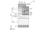
図1は、第1実施形態に係る半導体装置を例示する模式的断面図である。
図1に示すように、第1実施形態に係る半導体装置110は、第1電極51、第2電極52、第3電極53、半導体部材10及び第1結晶部材21を含む。
(First Embodiment)
FIG. 1 is a schematic cross-sectional view illustrating the semiconductor device according to the first embodiment.
As shown in FIG. 1, the
第1電極51から第2電極52への方向は、第1方向に沿う。第1方向をZ軸方向とする。Z軸方向に対して垂直な1つの方向をX軸方向とする。Z軸方向及びX軸方向に対して垂直な方向をY軸方向とする。
The direction from the
第3電極53の第1方向(Z軸方向)における位置は、第1電極51の第1方向における位置と、第2電極52の第1方向における位置と、の間にある。例えば、Z軸方向において、第3電極53の少なくとも一部が、第1電極51の少なくとも一部と、第2電極52の少なくとも一部と、の間にあっても良い。
The position of the
半導体部材10は、例えば、炭化シリコン、シリコン、カーボン及びゲルマニウムよりなる群から選択された少なくとも1つを含む。
The
半導体部材は、第1領域11、第1部分領域11a及び第2部分領域11bを含む。
The semiconductor member includes a
第1領域11は、第1方向(Z軸方向)において、第1電極51と第2電極52との間にある。第1領域11から第3電極53への第2方向は、第1方向(Z軸方向)と交差する。第2方向は、例えば、X軸方向である。
The
第1部分領域11aは、第1方向(Z軸方向)において、第1電極51と第1領域11との間にある。第1部分領域11aから第2部分領域11bへの方向は、第2方向(X軸方向)に沿う。第2部分領域11bは、第1方向(Z軸方向)において、第1電極51と第3電極53との間にある。
The first
第1結晶部材21は、第2方向(例えば、X軸方向)において、第1領域11と第3電極53との間に設けられる。
The
この例では、半導体部材10は、基板10sをさらに含む。基板10sは、第1電極51と第1部分領域11aとの間、及び、第1電極51と第2部分領域11bとの間に設けられる。基板10sは、例えば、SiC基板である。基板10sは、例えば、4H-SiC、または、6H-SiCを含む。
In this example, the
例えば、基板10sを含む半導体部材10にトレンチが形成され、トレンチの中に、第1結晶部材21及び第3電極53が設けられる。例えば、トレンチの側面に第1結晶部材21が形成される。残余の空間の少なくとも一部に、第3電極53が形成される。
For example, a trench is formed in the
第1結晶部材21は、分極を有する。1つの例において、第1結晶部材21は、ウルツ鉱構造を有する。別の例において、第1結晶部材21は、分極を有する他の結晶構造を有する。
The
例えば、第1結晶部材21における分極に基づいて、半導体部材10にキャリア領域(図1の例では、2次元電子ガス10e)が生じる。
For example, a carrier region (two-
第1電極51は、例えば、ドレイン電極として機能する。第2電極52は、例えば、ソース電極として機能する。第3電極53は、例えば、ゲート電極として機能する。半導体装置110は、例えば、トランジスタ(例えばHEMT:high electron mobility transistor)である。
The
例えば、第3電極53に印加される電圧により、第1電極51と第2電極52との間に流れる電流が制御できる。第1領域11は、電流経路の一部となる。
For example, the voltage applied to the
実施形態においては、半導体部材10は、X軸方向で第3電極53と対向する第1領域11に加えて、Z軸方向で第3電極53と第1電極51との間の領域(第2部分領域11b)を含む。そして、第1領域11と第2部分領域11bとを接続するように、第1部分領域11aが設けられている。このため、第1部分領域11a及び第2部分領域11bは、電流経路として機能する。第2部分領域11bにおいては、電流はX軸方向に広がりながら流れる。例えば、電流経路の断面積が拡大する。これにより、オン抵抗が低くできる。実施形態によれば、特性の向上が可能な半導体装置が提供できる。半導体装置110の特性の例については後述する。
In the embodiment, the
図1の例では、第1結晶部材21は、ウルツ鉱構造を有する。第1結晶部材は、例えば、AlxGa1-xN(0<x≦1)を含む。第1結晶部材は、例えば、AlNまたはAlGaNなどである。
In the example of FIG. 1, the
図1の例では、第1結晶部材21の<0001>方向は、第2方向(例えば、X軸方向)に沿う。<0001>方向とZ軸方向との間の角度の絶対値は、例えば、45度を超える。後述するように、第1結晶部材21の<000-1>方向が、第2方向(例えば、X軸方向)に沿っても良い。
In the example of FIG. 1, the <0001> direction of the
本願明細書における結晶方位の記載において、「-」は、バーを示す。例えば、「-1」は、バーを有する「1」に対応する。 In the description of the crystal orientation in the present specification, "-" indicates a bar. For example, "-1" corresponds to "1" having a bar.
例えば、第1結晶部材21の<0001>方向は、第1領域11から第3電極53への向きの成分を有する。このとき、半導体部材10のうちの第3電極53の近傍領域に、キャリア領域として、2次元電子ガス10eが生じる。
For example, the <0001> direction of the
第1結晶部材21は、ウルツ鉱構造でない結晶構造を有しても良い。第1結晶部材21は、例えば、BaTiO3、PbTiO3、Pb(Zrx,Ti1-x)O3、KNbO3、LiNbO3、LiTaO3、NaxWO3、ZnO、Ba2NaNb5O5、Pb2KNb5O15及びLi2B4O7からなる群から選択された少なくとも1つを含む。第1結晶部材21の分極の負から正への向き、または、分極の正から負への向きは、例えば、第2方向(X軸方向)に沿う。以下では、第1結晶部材21がウルツ鉱構造を有する場合の例について説明する。
The
図1に示すように、半導体装置110において、半導体部材10は、第1部分p1及び第2部分p2を含んでも良い。第1部分p1は、第1方向(Z軸方向)において、第1領域11と第2電極52との間に設けられる。第2部分p2は、第1方向(Z軸方向)において、第1部分p1と第2電極52との間に設けられる。第2部分p2における不純物濃度は、第1部分p1における不純物濃度よりも高い。
As shown in FIG. 1, in the
例えば、第2部分p2は、第2電極52とのコンタクト領域として機能する。この例では、第2部分p2の導電形は、n形である。
For example, the second portion p2 functions as a contact region with the
第1結晶部材21の<0001>方向が、第1領域11から第3電極53への向きの成分を有する場合(図1参照)、第1領域11はp形であることが好ましい。これにより、例えば、しきい値電圧を上昇させることができる。例えば、ノーマリオフ動作が得られる。
When the <0001> direction of the
第1領域11と第2部分p2との間の第1部分p1における不純物濃度は、第1領域11よりも低く、第2部分p2よりも低いことが好ましい。これにより、例えば、オフ電流(例えば、リーク電流)を抑制できる。
The impurity concentration in the first portion p1 between the
一方、基板10sの導電形は、第1領域11の導電形と逆である。この例では、第1領域11は、p形であり、第2部分p2は、n+形であり、基板10sは、n+形である。
On the other hand, the conductive type of the
第1部分領域11a及び第2部分領域11bは、例えば、ドリフト領域11dとして機能する。第1部分領域11a及び第2部分領域11bにおける不純物濃度は、第1領域11における不純物濃度よりも低い。
The first
第1部分領域11a及び第2部分領域11bは、例えば、4H-SiC、または、6H-SiCを含む。半導体部材10は、例えば、4H-SiC、または、6H-SiCを含む。
The first
半導体装置110においては、第1絶縁部材41が設けられている。第1絶縁部材41は、第2部分領域11bと第3電極53との間に設けられる。第1絶縁部材41は、第3電極53と半導体部材10(第2部分領域11bなど)とを電気的に絶縁する。後述するように、第1絶縁部材41は省略されても良い。
The
図1の例では、半導体装置110は、第2絶縁部材42をさらに含む。第2絶縁部材42は、第1方向(Z軸方向)において、第3電極53と、第2電極52の一部と、の間に設けられている。第2絶縁部材42は、第2電極52と第3電極53とを電気的に絶縁する。
In the example of FIG. 1, the
図1に示すように、第1領域11は、面11Fを含む。面11Fは、第1結晶部材21と対向する。第1結晶部材21は、第1面21Fを含む。第1面21Fは、第1領域11と対向する。例えば、第1面21Fは、面11Fと接する。第1面21Fは、第1方向(Z軸方向)に沿う。
As shown in FIG. 1, the
第1結晶部材21がウルツ鉱構造を有する場合、例えば、第1面21Fは、c面に沿う。第1面21Fは、c面に対して実質的に平行でも良い。第1面21Fとc面との間の角度は、例えば、45度未満である。第1面21Fとc面との間の角度は、例えば、10度以下である。基板10sの表面(例えば、第1電極51側の面でも良い)は、例えば、a面またはm面に沿っても良い。
When the
図2は、第1実施形態に係る半導体装置の特性を例示する模式図である。
図2は、半導体装置110のオン時における電子密度のシミュレーション結果を例示している。図2において、画像の明暗は、電子密度の高低に対応する。画像が暗い部分における電子密度は、画像が明るい部分における電子密度よりも高い。図2に示すように、電子密度は、第1部分領域11aと第3電極53との間の領域において高い。電子密度の高い領域は、第2部分領域11bで広がり、第3電極53の下側に広がっている。実施形態においては、第2部分領域11bにより、電子密度が高い領域が得られる。実施形態においては、第2部分領域11bが設けられない場合に比べて、オン抵抗を低くできる。
FIG. 2 is a schematic diagram illustrating the characteristics of the semiconductor device according to the first embodiment.
FIG. 2 illustrates the simulation result of the electron density when the
図3は、第1実施形態に係る半導体装置を例示する模式的断面図である。
以下、実施形態に係る半導体装置111について、半導体装置110とは異なる部分について説明する。半導体装置111においても、例えば、第1結晶部材21は、ウルツ鉱構造を有する。半導体装置111においては、第1結晶部材21の<000-1>方向は、第1領域11から第3電極53への向きの成分を有する。このとき、半導体部材10のうちの第3電極53の近傍領域に、キャリア領域として、2次元ホールガス10hが生じる。半導体装置111においても、第2部分領域11bが設けられることにより、オン抵抗を低くできる。特性の向上が可能な半導体装置を提供できる。
FIG. 3 is a schematic cross-sectional view illustrating the semiconductor device according to the first embodiment.
Hereinafter, the
半導体装置111においては、第1領域11は、n形であることが好ましい。これにより、例えば、しきい値電圧を上昇させることができる。例えば、ノーマリオフ動作が得られる。
In the
半導体装置111の1つの例において、第2部分p2は、p+形である。基板10sは、例えば、p+形である。
In one example of the
半導体装置111において、第1結晶部材21は、ウルツ鉱構造以外の、分極を有する結晶構造を有しても良い。この場合、第1結晶部材21の分極の負から正への向き、または、第1結晶部材21の分極の正から負への向きが、第2方向(X軸方向)に沿っても良い。
In the
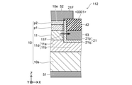
図4は、第1実施形態に係る半導体装置を例示する模式的断面図である。
以下、実施形態に係る半導体装置112について、半導体装置110とは異なる部分について説明する。半導体装置112においては、第1絶縁部材41が設けられていない。半導体装置112においては、第1結晶部材21は、複数の領域(領域21p及び領域21q)を含む。領域21pは、第2方向(X軸方向)において、第1領域11と第3電極53との間にある。領域21qは、第1方向(Z軸方向)において、第2部分領域11bと第3電極53との間にある。領域21qは、第2部分領域11bと第3電極53とを電気的に絶縁する。
FIG. 4 is a schematic cross-sectional view illustrating the semiconductor device according to the first embodiment.
Hereinafter, the
図5は、第1実施形態に係る半導体装置を例示する模式的断面図である。
以下、実施形態に係る半導体装置113について、半導体装置111とは異なる部分について説明する。半導体装置113においても、第1絶縁部材41が設けられていない。半導体装置113においても、第1結晶部材21は、領域21p及び領域21qを含む。領域21pは、第2方向において、第1領域11と第3電極53との間にある。領域21qは、第1方向において、第2部分領域11bと第3電極53との間にある。領域21qは、第2部分領域11bと第3電極53とを電気的に絶縁する。
FIG. 5 is a schematic cross-sectional view illustrating the semiconductor device according to the first embodiment.
Hereinafter, the
半導体装置112及び113においても、オン抵抗を低くできる。特性の向上が可能な半導体装置を提供できる。
The on-resistance can also be lowered in the
(第2実施形態)
図6は、第2実施形態に係る半導体装置を例示する模式的断面図である。
図6に示すように、第2実施形態に係る半導体装置120は、第1電極51、第2電極52、第3電極53、第4電極54、第5電極55、半導体部材10、第1結晶部材21及び第2結晶部材22を含む。
(Second Embodiment)
FIG. 6 is a schematic cross-sectional view illustrating the semiconductor device according to the second embodiment.
As shown in FIG. 6, the
第1電極51から第2電極52への方向は、第1方向に沿う。第1方向は、例えば、Z軸方向である。
The direction from the
第3電極53の第1方向(Z軸方向)における位置は、第1電極51の第1方向における位置と、第2電極52の第1方向における位置と、の間にある。
The position of the
第1電極51から第4電極54への方向は、第1方向(Z軸方向)に沿う。第2電極52から第4電極54への方向は、第2方向に沿う。第2方向は、第1方向と交差する。第2方向は、例えば、X軸方向である。
The direction from the
第5電極55の第1方向(Z軸方向)における位置は、第1電極51の第1方向における位置と、第4電極54の第1方向における位置と、の間にある。第3電極53から第5電極55への方向は、第2方向(例えばX軸方向)に沿う。
The position of the
半導体部材10は、炭化シリコン、シリコン、カーボン及びゲルマニウムよりなる群から選択された少なくとも1つを含む。半導体部材10は、第1領域11及び第2領域12を含む。第1領域11は、第1方向(Z軸方向)において、第1電極51と第2電極52との間にある。第2領域12は、第1方向(Z軸方向)において、第1電極51と第4電極54との間にある。例えば、第1領域11から第2領域12への方向は、X軸方向に沿う。
The
第1結晶部材21は、第2方向(例えばX軸方向)において、第1領域11と第3電極53との間に設けられる。第2結晶部材22は、第2方向において、第2領域12と第5電極55との間に設けられる。
The
第1電極51は、例えば、ドレイン電極として機能する。第2電極52は、例えば、1つのソース電極として機能する。第3電極53は、例えば、1つのゲート電極として機能する。第4電極54は、例えば、別のソース電極として機能する。第5電極55は、例えば、別のゲート電極として機能する。半導体装置120は、例えば、トランジスタ(例えばHEMT)である。
The
半導体装置120において、例えば、第1結晶部材21及び第2結晶部材22は、ウルツ鉱構造を有する。例えば、第1結晶部材の<0001>方向または<000-1>方向は、第2方向(X軸方向)に沿う。第2結晶部材の<0001>方向または<000-1>方向は、第2方向(X軸方向)に沿う。
In the
図6に示す例では、第1結晶部材21の<0001>方向は、第1領域11から第3電極53への向きの成分を有する。第2結晶部材22の<0001>方向は、第2領域12から第5電極55への向きの成分を有する。
In the example shown in FIG. 6, the <0001> direction of the
この場合、第1領域11の第3電極53と対向する領域、及び、第2領域12の第5電極55と対向する領域に、2次元電子ガス10eが生じる。2次元電子ガス10eは、電流経路として機能する。
In this case, the two-
実施形態においては、1つの半導体部材10に複数の電流経路が形成される。これにより、大電流のスイッチングが可能になる。例えば、オン抵抗を低くできる。本実施形態によれば、特性の向上が可能な半導体装置を提供できる。
In the embodiment, a plurality of current paths are formed in one
第1領域11は、例えば、第1結晶部材21と接する。第2領域12は、第2結晶部材22と接する。
The
半導体装置120において、第1結晶部材21及び第2結晶部材22は、ウルツ鉱構造以外の、分極を有する結晶構造を有しても良い。この場合、第1結晶部材21及び第2結晶部材22の分極の負から正への向き、または、第1結晶部材21及び第2結晶部材22の分極の正から負への向きが、第2方向(X軸方向)に沿っても良い。
In the
半導体装置120において、半導体部材10は、第1部分領域11a、第2部分領域11b、第3部分領域12c及び第4部分領域12dをさらに含んでも良い。これらの部分領域は、例えば、ドリフト領域として機能する。
In the
第1部分領域11aは、第1方向(Z軸方向)において、第1電極51と第1領域11との間にある。第1部分領域11aから第2部分領域11bへの方向は、第2方向(例えばX軸方向)に沿う。第2部分領域11bは、第1方向において、第1電極51と第3電極53との間にある。
The first
第3部分領域12cは、第1方向(Z軸方向)において、第1電極51と第2領域12との間にある。第3部分領域12cから第4部分領域12dへの方向は、第2方向(例えばX軸方向)に沿う。第4部分領域12dは、第1方向において、第1電極51と第5電極55との間にある。
The third
第2部分領域11b及び第4部分領域12dが設けられることで、例えば、電流経路が広がる。これにより、オン抵抗をより低くできる。
By providing the second
半導体装置120の1つの例において、半導体部材10は、第3領域13をさらに含んでも良い。第3領域13は、第2方向(X軸方向)において、第3電極53と第2領域12との間にある。第3領域13における不純物濃度は、第2領域12における不純物濃度よりも高い。第3領域13における不純物濃度は、第1領域11における不純物濃度よりも高い。
In one example of the
例えば、第1領域11及び第2領域12は、p形領域である。第3領域13は、p+領域である。第3領域13は、例えば、第3電極53と接しても良い。第3領域13は、第3電極53のコンタクト領域として機能しても良い。
For example, the
半導体装置120において、半導体部材10は、第4領域14をさらに含んでも良い。例えば、第2方向(X軸方向)において、第2領域12と第4領域14との間に、第5電極55が位置する。第4領域14は、p+領域である。第4領域14は、例えば、第5電極55と接しても良い。第4領域14は、第5電極55のコンタクト領域として機能しても良い。
In the
半導体装置120において、半導体部材10は、基板10sをさらに含んでも良い。基板10sは、第1電極51と第1領域11との間、及び、第1電極51と第2領域12との間に設けられる。基板10sは、第1電極51と第3領域13との間、及び、第1電極51と第4領域14との間に設けられる。基板10sは、例えば、SiC基板である。基板10sは、例えば、4H-SiC、または、6H-SiCを含む。半導体部材10は、例えば、4H-SiC、または、6H-SiCを含む。
In the
例えば、基板10sを含む半導体部材10に複数のトレンチが形成され、複数のトレンチの中に、結晶部材及び電極が設けられる。例えば、1つのトレンチの側面に第1結晶部材21が形成される。そのトレンチの残余の空間の少なくとも一部に、第3電極53が形成される。例えば、別のトレンチの側面に第2結晶部材22が形成される。そのトレンチの残余の空間の少なくとも一部に、第5電極55が形成される。
For example, a plurality of trenches are formed in the
例えば、第3領域13の一部は、基板10sと第3電極53との間に設けられても良い。例えば、第4領域14の一部は、基板10sと第5電極55との間に設けられても良い。
For example, a part of the
半導体部材10は、第1~第4部分p1~p4をさらに含んでも良い。第1部分p1は、第1方向(Z軸方向)において、第1領域11と第2電極52との間に設けられる。第2部分p2は、第1方向において、第1部分p1と第2電極52との間に設けられる。第3部分p3は、第1方向(Z軸方向)において、第2領域12と第4電極54との間に設けられる。第4部分p4は、第1方向において、第3部分p3と第4電極54との間に設けられる。
The
第2部分p2における不純物濃度は、第1部分p1における不純物濃度よりも高い。第4部分p4における不純物濃度は、第3部分p3における不純物濃度よりも高い。第1部分p1における不純物濃度は、例えば、第1領域11における不純物濃度よりも低い。第3部分p3における不純物濃度は、例えば、第2領域12における不純物濃度よりも低い。
The impurity concentration in the second portion p2 is higher than the impurity concentration in the first portion p1. The impurity concentration in the fourth portion p4 is higher than the impurity concentration in the third portion p3. The impurity concentration in the first portion p1 is, for example, lower than the impurity concentration in the
1つの例において、第1領域11及び第2領域12は、p形である。第2部分p2及び第4部分p4は、例えば、n+形である。第3領域13及び第4領域14は、例えば、p+形である。基板10sは、例えば、n+形である。
In one example, the
半導体装置120において、第1~第4絶縁部材41~44が設けられても良い。第1絶縁部材41は、第2部分領域11bと第3電極53との間に設けられる。この例では、第1絶縁部材41は、第1方向(Z軸方向)において、第3領域13の一部と第3電極53との間に設けられる。
In the
第2絶縁部材42は、第1方向(Z軸方向)において、第3電極53と、第2電極52の一部と、の間に設けられている。第2絶縁部材42は、第2電極52と第3電極53とを電気的に絶縁する。第2絶縁部材42は、第2電極52と第3領域13とを電気的に絶縁する。
The second insulating
第3絶縁部材43は、第4部分領域12dと第5電極55との間に設けられる。この例では、第3絶縁部材43は、第1方向(Z軸方向)において、第4領域14の一部と第5電極55との間に設けられる。
The third insulating
第4絶縁部材44は、第1方向(Z軸方向)において、第5電極55と、第4電極54の一部と、の間に設けられている。第4絶縁部材44は、第4電極54と第5電極55とを電気的に絶縁する。第4絶縁部材44は、第4電極54と第4領域14とを電気的に絶縁する。
The fourth insulating
図7は、第2実施形態に係る半導体装置を例示する模式的断面図である。
以下、実施形態に係る半導体装置121について、半導体装置120とは異なる部分について説明する。半導体装置121においても、第1結晶部材21は、ウルツ鉱構造を有する。半導体装置121においては、第1結晶部材21の<000-1>方向は、第1領域11から第3電極53への向きの成分を有する。第2結晶部材22の<000-1>方向は、第2領域12から第5電極55への向きの成分を有する。このとき、半導体部材10のうちの第3電極53の近傍領域、及び、第5電極55の近傍領域に、キャリア領域として、2次元ホールガス10hが生じる。半導体装置121においても、オン抵抗を低くできる。半導体装置121において、第2部分領域11b及び第4部分領域12dが設けられることにより、オン抵抗をさらに低くできる。特性の向上が可能な半導体装置を提供できる。
FIG. 7 is a schematic cross-sectional view illustrating the semiconductor device according to the second embodiment.
Hereinafter, the
半導体装置121の1つの例において、第1領域11及び第2領域12は、n形である。第2部分p2及び第4部分p4は、例えば、p+形である。第3領域13及び第4領域14は、例えば、n+形である。基板10sは、例えば、p+形である。
In one example of the
半導体装置121において、第1結晶部材21及び第2結晶部材22は、ウルツ鉱構造以外の、分極を有する結晶構造を有しても良い。この場合、第1結晶部材21及び第2結晶部材22の分極の負から正への向き、または、第1結晶部材21及び第2結晶部材22の分極の正から負への向きが、第2方向(X軸方向)に沿っても良い。
In the
以下、半導体装置120の特性の例について説明する。図6に示すように、第1領域11と第1結晶部材21との間の境界と、第2部分領域11bと第3領域13との境界と、の間のX軸方向に沿う距離を距離dxとする。以下、図6に例示した半導体装置120において、距離dxを変えたときの特性のシミュレーション結果の例について説明する。
Hereinafter, an example of the characteristics of the
図8は、第2実施形態に係る半導体装置の特性を例示するグラフ図である。
図8の横軸は、ゲート電圧Vg(V)である。ゲート電圧Vgは、第2電極52(ソース電極)を規準にしたときの第3電極53(ゲート電極)の電位に対応する。図8の縦軸は、ドレイン電流Id(×10-6A)である。図8には、距離dxが0nm、150nm、300nmまたは400nmのときの結果が例示されている。この例では、第3電極53のX軸方向の長さは、800nmである。図8から分かるように、距離dxが長くなると、同じゲート電圧Vgにおけるドレイン電流Idが大きくなる。
FIG. 8 is a graph illustrating the characteristics of the semiconductor device according to the second embodiment.
The horizontal axis of FIG. 8 is the gate voltage Vg (V). The gate voltage Vg corresponds to the potential of the third electrode 53 (gate electrode) when the second electrode 52 (source electrode) is used as a reference. The vertical axis of FIG. 8 is the drain current Id (× 10 -6 A). FIG. 8 illustrates the results when the distance dx is 0 nm, 150 nm, 300 nm or 400 nm. In this example, the length of the
以下、図6に例示した半導体装置120において、第1領域11(例えばp形領域)における不純物濃度を変えたときの特性のシミュレーション結果の例について説明する。
Hereinafter, in the
図9は、第2実施形態に係る半導体装置の特性を例示するグラフ図である。
図9の横軸は、ゲート電圧Vg(V)である。図9の縦軸は、ドレイン電流Id(×10-5A)である。図9には、第1領域11におけるp形の不純物濃度Cpが、5×1017cm-3、7×1017cm-3、8×1017cm-3、または、9×1017cm-3のときの特性が例示されている。図9から分かるように、不純物濃度が低いと、ゲート電圧Vgが0Vのときのドレイン電流Id大きい。第1領域11における不純物濃度を制御することで、しきい値電圧を制御できる。半導体装置120の1つの例において、第1領域11におけるp形の不純物濃度Cpは、7×1017cm-3以上であることが好ましい。これにより、例えば、オフ電流を小さくできる。安定したノーマリオフ特性が得られる。
FIG. 9 is a graph illustrating the characteristics of the semiconductor device according to the second embodiment.
The horizontal axis of FIG. 9 is the gate voltage Vg (V). The vertical axis of FIG. 9 is the drain current Id (× 10 -5 A). In FIG. 9, the p-type impurity concentration Cp in the
図10は、第2実施形態に係る半導体装置を例示する模式的断面図である。
以下、実施形態に係る半導体装置122について、半導体装置120とは異なる部分について説明する。半導体装置122においては、第1絶縁部材41及び第3絶縁部材43が設けられていない。
FIG. 10 is a schematic cross-sectional view illustrating the semiconductor device according to the second embodiment.
Hereinafter, the
半導体装置122においては、第1結晶部材21は、領域21p及び領域21qを含む。領域21pは、第2方向(X軸方向)において、第1領域11と第3電極53との間にある。領域21qは、第1方向(Z軸方向)において、第2部分領域11bと第3電極53との間にある。領域21qは、第2部分領域11bと第3電極53とを電気的に絶縁する。
In the
半導体装置122においては、第2結晶部材22は、領域22p及び領域22qを含む。領域22pは、第2方向(X軸方向)において、第2領域12と第5電極55との間にある。領域22qは、第1方向(Z軸方向)において、第4部分領域12dと第5電極55との間にある。領域22qは、第4部分領域12dと第5電極55とを電気的に絶縁する。
In the
図11は、第2実施形態に係る半導体装置を例示する模式的断面図である。
以下、実施形態に係る半導体装置123について、半導体装置121とは異なる部分について説明する。半導体装置123においても、第1絶縁部材41及び第3絶縁部材43が設けられていない。半導体装置122においては、第1結晶部材21は、領域21p及び領域21qを含む。第2結晶部材22は、領域22p及び領域22qを含む。
FIG. 11 is a schematic cross-sectional view illustrating the semiconductor device according to the second embodiment.
Hereinafter, the
半導体装置122及び123においても、オン抵抗を低くできる。特性の向上が可能な半導体装置を提供できる。
The on-resistance can also be lowered in the
(第3実施形態)
図12は、第3実施形態に係る半導体装置を例示する模式的断面図である。
図12に示すように、第3実施形態に係る半導体装置130は、第1電極51、第2電極52、第3電極53、第4電極54、半導体部材10、第1結晶部材21及び第2結晶部材22を含む。
(Third Embodiment)
FIG. 12 is a schematic cross-sectional view illustrating the semiconductor device according to the third embodiment.
As shown in FIG. 12, the
第3電極53から第4電極54への第1方向は、第1電極51から第2電極52への第2方向と交差する。
The first direction from the
第1方向をZ軸方向とする。第2方向は、例えば、X軸方向である。 The first direction is the Z-axis direction. The second direction is, for example, the X-axis direction.
第3電極53の第2方向(X軸方向)における位置は、第1電極51の第2方向における位置と、第2電極52の第2方向における位置と、の間にある。例えば、X軸方向において、第3電極53は、第1電極51と第2電極52との間にある。
The position of the
第4電極54の第2方向(X軸方向)における位置は、第1電極51の第2方向における位置と、第2電極52の第2方向における位置と、の間にある。例えば、第4電極54は、第3電極53の上方に設けられる。
The position of the
半導体部材10は、炭化シリコン、シリコン、カーボン及びゲルマニウムよりなる群から選択された少なくとも1つを含む。
The
この例では、基板10sが設けられる。基板10sの上に、半導体部材10、及び、第1~第4電極51~54が設けられる。基板10sは、例えば、SiC基板である。基板10sは、例えば、4H-SiC、または、6H-SiCを含む。半導体部材10は、例えば、4H-SiC、または、6H-SiCを含む。
In this example, the
半導体部材10は、第1領域11及び第2領域12を含む。第1領域11は、第2方向(X軸方向)において、第1電極51と第3電極53との間にある。第2領域12は、第2方向において、第3電極53と第2電極52との間にある。第1領域11及び第2領域12は、第4電極54と電気的に接続される。
The
第1結晶部材21は、第2方向(X軸方向)において、第1領域11と第3電極53との間に設けられる。第2結晶部材22は、第2方向において、第2領域12と第3電極53との間に設けられる。
The
例えば、第1結晶部材21及び第2結晶部材22は、ウルツ鉱構造を有する。第1結晶部材21の<0001>方向は、第1領域11から第3電極53への向きの成分を有する。第2結晶部材22の<0001>方向は、第3電極53から第2領域12への向きの成分を有する。
For example, the
例えば、第1領域11のうちの第1結晶部材21の近傍領域に、2次元電子ガス10eが形成される。例えば、第2領域12のうちの第2結晶部材22の近傍領域に、2次元ホールガス10hが形成される。
For example, the two-
例えば、第1電極51の電位が低電位に設定される。第2電極52の電位が高電位に設定される。この高電位は、上記の低電位よりも高い。第3電極53に入力信号が入力される。入力信号に応じて、第1電極51と第4電極54との間の抵抗状態、及び、第2電極52と第4電極54との間の抵抗状態が制御される。これにより、入力信号に応じた信号が第4電極54から出力される。半導体装置130は、例えば、CMOS(Complementary metal-oxide-semiconductor)素子として機能する。半導体装置130において、例えば、高速のスイッチング特性が得られる。例えば、消費電力を低くできる。特性の向上が可能な半導体装置を提供できる。
For example, the potential of the
この例では、半導体部材10は、第1~第4部分p1~p4をさらに含む。第1部分p1は、第1方向(Z軸方向)において、第1領域11と第4電極54との間に設けられる。第2部分p2は、第1方向において、第1部分p1と第4電極54との間に設けられる。第3部分p3は、第1方向(Z軸方向)において、第2領域12と第4電極54との間に設けられる。第4部分p4は、第1方向において、第3部分p3と第4電極54との間に設けられる。
In this example, the
第2部分p2における不純物濃度は、第1部分p1における不純物濃度よりも高い。第4部分p4における不純物濃度は、第3部分p3における不純物濃度よりも高い。第1部分p1における不純物濃度は、例えば、第1領域11における不純物濃度よりも低い。第3部分p3における不純物濃度は、例えば、第2領域12における不純物濃度よりも低い。
The impurity concentration in the second portion p2 is higher than the impurity concentration in the first portion p1. The impurity concentration in the fourth portion p4 is higher than the impurity concentration in the third portion p3. The impurity concentration in the first portion p1 is, for example, lower than the impurity concentration in the
第2部分p2及び第4部分p4は、第4電極54に対するコンタクト領域として機能する。
The second portion p2 and the fourth portion p4 function as a contact region with respect to the
半導体部材10は、第3領域13及び第4領域14をさらに含む。この例では、基板10sの一部に不純物濃度が高い領域が設けられる。この不純物濃度が高い領域が、第3領域13及び第4領域14に対応する。例えば、第3領域13の一部から第1電極51への方向は、第1方向(Z軸方向)に沿う。例えば、第4領域14の一部から第2電極52への方向は、第1方向(Z軸方向)に沿う。第3領域13は、第1電極51と第1領域11との間の電流経路となる。第4領域14は、第2電極52と第2領域12との間の電流経路となる。
The
この例では、半導体部材10は、第5部分p5及び第6部分p6をさらに含む。第5部分p5は、第1方向(Z軸方向)において、第3領域13の別の一部と、第1領域11との間にある。第6部分p6は、第1方向(Z軸方向)において、第4領域14の別の一部と、第2領域12との間にある。
In this example, the
第3領域13は、例えば、n+領域である。第4領域14は、例えば、p+領域である。第1領域11は、例えば、p形領域である。第2領域12は、例えば、n形領域である。第2部分p2は、例えば、n+形領域である。第4部分p4は、p+形領域である。
The
この例では、第1~第4絶縁部材41~44が設けられている。第1絶縁部材41は、基板10s(第3領域13及び第4領域14を含む)と、第3電極53と、の間に設けられる。第2絶縁部材42は、第3電極53と第4電極54との間、第1結晶部材21と第4電極54との間、及び、第2結晶部材22と第4電極54との間に設けられる。
In this example, the first to fourth insulating
第3絶縁部材43は、第2方向(X軸方向)において、第1電極51と第1領域11との間、第1電極51と第1部分p1との間、第1電極51と第2部分p2との間、第1電極51と第5部分p5との間に設けられる。
The third insulating
第4絶縁部材44は、第2方向(X軸方向)において、第2電極52と第2領域12との間、第2電極52と第3部分p3との間、第2電極52と第4部分p4との間、第2電極52と第6部分p6との間に設けられる。
The fourth insulating
半導体装置130において、第1結晶部材21及び第2結晶部材22は、ウルツ鉱構造以外の、分極を有する結晶構造を有しても良い。この場合、第1結晶部材21及び第2結晶部材22の分極の負から正への向き、または、第1結晶部材21及び第2結晶部材22の分極の正から負への向きが、第2方向(X軸方向)に沿っても良い。
In the
図13は、第3実施形態に係る半導体装置を例示する模式的断面図である。
以下、実施形態に係る半導体装置131について、半導体装置130とは異なる部分について説明する。半導体装置131においては、第1絶縁部材41が設けられない。半導体装置131は、第1結晶部材21及び第2結晶部材22に、加えて、第3結晶部材23をさらに含む。
FIG. 13 is a schematic cross-sectional view illustrating the semiconductor device according to the third embodiment.
Hereinafter, the
第1方向(Z軸方向)おいて、第3結晶部材23と第4電極54との間に第3電極53が設けられる。第2絶縁部材42が設けられる場合、第1方向(Z軸方向)おいて、第3結晶部材23と第2絶縁部材42との間に第3電極53が設けられる。
In the first direction (Z-axis direction), the
第3結晶部材23は、第1結晶部材21と同じ材料を含んでも良い。第3結晶部材23は、第2結晶部材22と同じ材料を含んでも良い。第3結晶部材23は、第1結晶部材21及び第2結晶部材22と連続しても良い。第3結晶部材23は、例えば、第3電極53と、基板10s(第3領域13及び第4領域14を含む)と、を電気的に絶縁する。例えば、第1~第3結晶部材21~23は、絶縁性である。
The
半導体装置131も、例えば、CMOS素子として機能する。半導体装置131において、例えば、高速のスイッチング特性が得られる。例えば、消費電力を低くできる。特性の向上が可能な半導体装置を提供できる。
The
上記の実施形態において、電極(例えば、第1~第5電極51~55の少なくともいずれか)は、例えば、Al、Ti、Ni及びAuよりなる群から選択された少なくとも1つを含む。
In the above embodiment, the electrode (for example, at least one of the first to
上記の実施形態において、半導体部材10は、例えば、SiCを含む。この場合、半導体部材10がシリコンを含む場合に比べて、高い放熱性が得られる。
In the above embodiment, the
結晶部材(第1結晶部材21及び第2結晶部材22)は、AlNを含むことが好ましい。これにより、高い耐圧が得られる。
The crystal member (
半導体部材10がSiCを含み、結晶部材がAlNを含む場合ことが好ましい。これらの材料における格子定数差が小さい。例えば、AlN(結晶部材)において、良好な結晶性が得られる。
It is preferable that the
半導体部材10がSiCを含み、結晶部材がAlNを含む場合、これらの材料の間におけるポテンシャル差が大きい。これにより、キャリアが閉じこめられやすく、局在化し易い。例えば、キャリアの積分濃度を高くできる。
When the
上記の実施形態において、結晶部材は、例えば、MOCVD(有機金属気相)法、分子線エピタキシ(MBE)法、ハライド気相成長(HVPE)法、スパッタ法、及び、パルスレーザー堆積法よりなる群から選択された少なくとも1つにより形成される。 In the above embodiment, the crystal member is composed of, for example, a MOCVD (organic metal vapor phase) method, a molecular beam epitaxy (MBE) method, a halide vapor phase growth (HVPE) method, a sputtering method, and a pulsed laser deposition method. Formed by at least one selected from.
実施形態によれば、特性の向上が可能な半導体装置を提供することができる。 According to the embodiment, it is possible to provide a semiconductor device whose characteristics can be improved.
本願明細書において、「電気的に接続される状態」は、複数の導電体が物理的に接してこれら複数の導電体の間に電流が流れる状態を含む。「電気的に接続される状態」は、複数の導電体の間に、別の導電体が挿入されて、これらの複数の導電体の間に電流が流れる状態を含む。 As used herein, the "electrically connected state" includes a state in which a plurality of conductors are physically in contact with each other and a current flows between the plurality of conductors. The "electrically connected state" includes a state in which another conductor is inserted between the plurality of conductors and a current flows between the plurality of conductors.
本願明細書において、「垂直」及び「平行」は、厳密な垂直及び厳密な平行だけではなく、例えば製造工程におけるばらつきなどを含むものであり、実質的に垂直及び実質的に平行であれば良い。 In the present specification, "vertical" and "parallel" include not only strict vertical and strict parallel, but also variations in the manufacturing process, for example, and may be substantially vertical and substantially parallel. ..
以上、具体例を参照しつつ、本発明の実施の形態について説明した。しかし、本発明は、これらの具体例に限定されるものではない。例えば、半導体装置に含まれる、電極、半導体部材、結晶部材及び絶縁部材などの各要素の具体的な構成に関しては、当業者が公知の範囲から適宜選択することにより本発明を同様に実施し、同様の効果を得ることができる限り、本発明の範囲に包含される。 Hereinafter, embodiments of the present invention have been described with reference to specific examples. However, the present invention is not limited to these specific examples. For example, with respect to the specific configuration of each element such as an electrode, a semiconductor member, a crystal member, and an insulating member included in a semiconductor device, the present invention is similarly carried out by appropriately selecting from a range known to those skilled in the art. As long as a similar effect can be obtained, it is included in the scope of the present invention.
また、各具体例のいずれか2つ以上の要素を技術的に可能な範囲で組み合わせたものも、本発明の要旨を包含する限り本発明の範囲に含まれる。 Further, a combination of any two or more elements of each specific example to the extent technically possible is also included in the scope of the present invention as long as the gist of the present invention is included.
その他、本発明の実施の形態として上述した半導体装置を基にして、当業者が適宜設計変更して実施し得る全ての半導体装置も、本発明の要旨を包含する限り、本発明の範囲に属する。 In addition, all semiconductor devices that can be appropriately designed and implemented by those skilled in the art based on the semiconductor device described above as an embodiment of the present invention also belong to the scope of the present invention as long as the gist of the present invention is included. ..
その他、本発明の思想の範疇において、当業者であれば、各種の変更例及び修正例に想到し得るものであり、それら変更例及び修正例についても本発明の範囲に属するものと解される。 In addition, in the scope of the idea of the present invention, those skilled in the art can come up with various modified examples and modified examples, and it is understood that these modified examples and modified examples also belong to the scope of the present invention. ..
本発明のいくつかの実施形態を説明したが、これらの実施形態は、例として提示したものであり、発明の範囲を限定することは意図していない。これら新規な実施形態は、その他の様々な形態で実施されることが可能であり、発明の要旨を逸脱しない範囲で、種々の省略、置き換え、変更を行うことができる。これら実施形態やその変形は、発明の範囲や要旨に含まれるとともに、特許請求の範囲に記載された発明とその均等の範囲に含まれる。 Although some embodiments of the present invention have been described, these embodiments are presented as examples and are not intended to limit the scope of the invention. These novel embodiments can be implemented in various other embodiments, and various omissions, replacements, and changes can be made without departing from the gist of the invention. These embodiments and variations thereof are included in the scope and gist of the invention, and are also included in the scope of the invention described in the claims and the equivalent scope thereof.
10…半導体部材、 10e…2次元電子ガス、 10h…2次元ホールガス、 10s…基板、 11~14…第1~第4領域、 11F…面、 11a、11b…第1、第2部分領域、 11d…ドリフト領域、 12c、12d…第3、第4部分領域、 21~23…第1、第3結晶部材、 21F…第1面、 21p、21q、22p、22q…領域、 41~44…第1~第4絶縁部材、 51~55…第1~第5電極、 110~113、120~123、130、131…半導体装置、 Cp…不純物濃度、 Id…ドレイン電流、 Vg…ゲート電圧、 dx…距離、 p1~p6…第1~第6部分 10 ... Semiconductor member, 10e ... Two-dimensional electron gas, 10h ... Two-dimensional hall gas, 10s ... Substrate, 11-14 ... First to fourth regions, 11F ... Surface, 11a, 11b ... First, second partial regions, 11d ... Drift region, 12c, 12d ... Third and fourth partial regions, 21-23 ... First and third crystal members, 21F ... First plane, 21p, 21q, 22p, 22q ... Region, 41-44 ... First 1st to 4th insulating members, 51 to 55 ... 1st to 5th electrodes, 110 to 113, 120 to 123, 130, 131 ... semiconductor device, Cp ... impurity concentration, Id ... drain current, Vg ... gate voltage, dx ... Distance, p1 to p6 ... 1st to 6th parts
Claims (18)
第2電極であって、前記第1電極から前記第2電極への方向は、第1方向に沿う、前記第2電極と、
第3電極であって、前記第3電極の前記第1方向における位置は、前記第1電極の前記第1方向における位置と、前記第2電極の前記第1方向における位置と、の間にある、前記第3電極と、
炭化シリコン、シリコン、カーボン及びゲルマニウムよりなる群から選択された少なくとも1つを含む半導体部材であって、前記半導体部材は、第1領域、第1部分領域及び第2部分領域を含み、前記第1領域は、前記第1方向において前記第1電極と前記第2電極との間にあり、前記第1領域から前記第3電極への第2方向は、前記第1方向と交差し、前記第1部分領域は、前記第1方向において前記第1電極と前記第1領域との間にあり、前記第1部分領域から前記第2部分領域への方向は、前記第2方向に沿い、前記第2部分領域は、前記第1方向において前記第1電極と前記第3電極との間にある、前記半導体部材と、
前記第2方向において、前記第1領域と前記第3電極との間に設けられた第1結晶部材と、
を備え、
前記第3電極に印加される電圧により、前記第1電極と前記第2電極との間に流れる電流が制御でき、
前記第1結晶部材は、ウルツ鉱構造を有し、
前記第1結晶部材の<0001>方向または<000-1>方向は、前記第2方向に沿う、半導体装置。 With the first electrode
The second electrode, and the direction from the first electrode to the second electrode is along the first direction with the second electrode.
The position of the third electrode in the first direction of the third electrode is between the position of the first electrode in the first direction and the position of the second electrode in the first direction. , The third electrode and
A semiconductor member comprising at least one selected from the group consisting of silicon carbide, silicon, carbon and germanium, wherein the semiconductor member comprises a first region, a first partial region and a second partial region, said first. The region lies between the first electrode and the second electrode in the first direction, and the second direction from the first region to the third electrode intersects the first direction and is said to be the first. The partial region lies between the first electrode and the first region in the first direction, and the direction from the first partial region to the second partial region is along the second direction and the second. The partial region includes the semiconductor member located between the first electrode and the third electrode in the first direction.
In the second direction, the first crystal member provided between the first region and the third electrode, and
Equipped with
The voltage applied to the third electrode can control the current flowing between the first electrode and the second electrode.
The first crystal member has a wurtzite structure and has a wurtzite structure.
A semiconductor device in which the <0001> direction or the <000-1> direction of the first crystal member is along the second direction .
第2電極であって、前記第1電極から前記第2電極への方向は、第1方向に沿う、前記第2電極と、
第3電極であって、前記第3電極の前記第1方向における位置は、前記第1電極の前記第1方向における位置と、前記第2電極の前記第1方向における位置と、の間にある、前記第3電極と、
炭化シリコン、シリコン、カーボン及びゲルマニウムよりなる群から選択された少なくとも1つを含む半導体部材であって、前記半導体部材は、第1領域、第1部分領域及び第2部分領域を含み、前記第1領域は、前記第1方向において前記第1電極と前記第2電極との間にあり、前記第1領域から前記第3電極への第2方向は、前記第1方向と交差し、前記第1部分領域は、前記第1方向において前記第1電極と前記第1領域との間にあり、前記第1部分領域から前記第2部分領域への方向は、前記第2方向に沿い、前記第2部分領域は、前記第1方向において前記第1電極と前記第3電極との間にある、前記半導体部材と、
前記第2方向において、前記第1領域と前記第3電極との間に設けられた第1結晶部材と、
を備え、
前記第3電極に印加される電圧により、前記第1電極と前記第2電極との間に流れる電流が制御でき、
前記第1結晶部材の分極の負から正への向き、または、前記分極の正から負への向きは、前記第2方向に沿う、半導体装置。 With the first electrode
The second electrode, and the direction from the first electrode to the second electrode is along the first direction with the second electrode.
The position of the third electrode in the first direction of the third electrode is between the position of the first electrode in the first direction and the position of the second electrode in the first direction. , The third electrode and
A semiconductor member comprising at least one selected from the group consisting of silicon carbide, silicon, carbon and germanium, wherein the semiconductor member comprises a first region, a first partial region and a second partial region, said first. The region lies between the first electrode and the second electrode in the first direction, and the second direction from the first region to the third electrode intersects the first direction and is said to be the first. The partial region lies between the first electrode and the first region in the first direction, and the direction from the first partial region to the second partial region is along the second direction and the second. The partial region includes the semiconductor member located between the first electrode and the third electrode in the first direction.
In the second direction, the first crystal member provided between the first region and the third electrode, and
Equipped with
The voltage applied to the third electrode can control the current flowing between the first electrode and the second electrode.
A semiconductor device in which the direction of the polarization of the first crystal member from negative to positive or the direction of the polarization from positive to negative is along the second direction.
第2電極であって、前記第1電極から前記第2電極への方向は、第1方向に沿う、前記第2電極と、
第3電極であって、前記第3電極の前記第1方向における位置は、前記第1電極の前記第1方向における位置と、前記第2電極の前記第1方向における位置と、の間にある、前記第3電極と、
炭化シリコン、シリコン、カーボン及びゲルマニウムよりなる群から選択された少なくとも1つを含む半導体部材であって、前記半導体部材は、第1領域、第1部分領域及び第2部分領域を含み、前記第1領域は、前記第1方向において前記第1電極と前記第2電極との間にあり、前記第1領域から前記第3電極への第2方向は、前記第1方向と交差し、前記第1部分領域は、前記第1方向において前記第1電極と前記第1領域との間にあり、前記第1部分領域から前記第2部分領域への方向は、前記第2方向に沿い、前記第2部分領域は、前記第1方向において前記第1電極と前記第3電極との間にある、前記半導体部材と、
前記第2方向において、前記第1領域と前記第3電極との間に設けられた第1結晶部材と、
を備え、
前記第3電極に印加される電圧により、前記第1電極と前記第2電極との間に流れる電流が制御でき、
前記第1結晶部材は、ウルツ鉱構造を有し、
前記第1結晶部材の<0001>方向は、前記第1領域から前記第3電極への向きの成分を有し、
前記第1領域はp形である、半導体装置。 With the first electrode
The second electrode, and the direction from the first electrode to the second electrode is along the first direction with the second electrode.
The position of the third electrode in the first direction of the third electrode is between the position of the first electrode in the first direction and the position of the second electrode in the first direction. , The third electrode and
A semiconductor member comprising at least one selected from the group consisting of silicon carbide, silicon, carbon and germanium, wherein the semiconductor member comprises a first region, a first partial region and a second partial region, said first. The region lies between the first electrode and the second electrode in the first direction, and the second direction from the first region to the third electrode intersects the first direction and is said to be the first. The partial region lies between the first electrode and the first region in the first direction, and the direction from the first partial region to the second partial region is along the second direction and the second. The partial region includes the semiconductor member located between the first electrode and the third electrode in the first direction.
In the second direction, the first crystal member provided between the first region and the third electrode, and
Equipped with
The voltage applied to the third electrode can control the current flowing between the first electrode and the second electrode.
The first crystal member has a wurtzite structure and has a wurtzite structure.
The <0001> direction of the first crystal member has a component in the direction from the first region to the third electrode.
The first region is a p-shaped semiconductor device.
第2電極であって、前記第1電極から前記第2電極への方向は、第1方向に沿う、前記第2電極と、
第3電極であって、前記第3電極の前記第1方向における位置は、前記第1電極の前記第1方向における位置と、前記第2電極の前記第1方向における位置と、の間にある、前記第3電極と、
炭化シリコン、シリコン、カーボン及びゲルマニウムよりなる群から選択された少なくとも1つを含む半導体部材であって、前記半導体部材は、第1領域、第1部分領域及び第2部分領域を含み、前記第1領域は、前記第1方向において前記第1電極と前記第2電極との間にあり、前記第1領域から前記第3電極への第2方向は、前記第1方向と交差し、前記第1部分領域は、前記第1方向において前記第1電極と前記第1領域との間にあり、前記第1部分領域から前記第2部分領域への方向は、前記第2方向に沿い、前記第2部分領域は、前記第1方向において前記第1電極と前記第3電極との間にある、前記半導体部材と、
前記第2方向において、前記第1領域と前記第3電極との間に設けられた第1結晶部材と、
を備え、
前記第3電極に印加される電圧により、前記第1電極と前記第2電極との間に流れる電流が制御でき、
前記第1結晶部材は、ウルツ鉱構造を有し、
前記第1結晶部材の<000-1>方向は、前記第1領域から前記第3電極への向きの成分を有し、
前記第1領域はn形である、半導体装置。 With the first electrode
The second electrode, and the direction from the first electrode to the second electrode is along the first direction with the second electrode.
The position of the third electrode in the first direction of the third electrode is between the position of the first electrode in the first direction and the position of the second electrode in the first direction. , The third electrode and
A semiconductor member comprising at least one selected from the group consisting of silicon carbide, silicon, carbon and germanium, wherein the semiconductor member comprises a first region, a first partial region and a second partial region, said first. The region lies between the first electrode and the second electrode in the first direction, and the second direction from the first region to the third electrode intersects the first direction and is said to be the first. The partial region lies between the first electrode and the first region in the first direction, and the direction from the first partial region to the second partial region is along the second direction and the second. The partial region includes the semiconductor member located between the first electrode and the third electrode in the first direction.
In the second direction, the first crystal member provided between the first region and the third electrode, and
Equipped with
The voltage applied to the third electrode can control the current flowing between the first electrode and the second electrode.
The first crystal member has a wurtzite structure and has a wurtzite structure.
The <000-1> direction of the first crystal member has a component in the direction from the first region to the third electrode.
The first region is an n-type semiconductor device.
ソース電極であって、前記ドレイン電極から前記ソース電極への方向は、第1方向に沿う、前記ソース電極と、
ゲート電極であって、前記ゲート電極の前記第1方向における位置は、前記ドレイン電極の前記第1方向における位置と、前記ソース電極の前記第1方向における位置と、の間にある、前記ゲート電極と、
別のソース電極であって、前記ドレイン電極から前記別のソース電極への方向は、前記第1方向に沿い、前記ソース電極から前記別のソース電極への方向は、前記第1方向と交差する第2方向に沿う、前記別のソース電極と、
別のゲート電極であって、前記別のゲート電極の前記第1方向における位置は、前記ドレイン電極の前記第1方向における前記位置と、前記別のソース電極の前記第1方向における位置と、の間にあり、前記ゲート電極から前記別のゲート電極への方向は、前記第2方向に沿う、前記別のゲート電極と、
炭化シリコン、シリコン、カーボン及びゲルマニウムよりなる群から選択された少なくとも1つを含む半導体部材であって、前記半導体部材は、第1領域及び第2領域を含み、前記第1領域は、前記第1方向において前記ドレイン電極と前記ソース電極との間にあり、前記第2領域は、前記第1方向において前記ドレイン電極と前記別のソース電極との間にある、前記半導体部材と、
前記第2方向において、前記第1領域と前記ゲート電極との間に設けられた第1結晶部材と、
前記第2方向において、前記第2領域と前記別のゲート電極との間に設けられた第2結晶部材と、
を備えた半導体装置。 With the drain electrode
The source electrode, and the direction from the drain electrode to the source electrode is along the first direction with the source electrode.
The gate electrode, wherein the position of the gate electrode in the first direction is between the position of the drain electrode in the first direction and the position of the source electrode in the first direction. When,
Another source electrode, the direction from the drain electrode to the other source electrode is along the first direction, and the direction from the source electrode to the other source electrode intersects the first direction. With the other source electrode along the second direction,
In the other gate electrode, the position of the other gate electrode in the first direction is the position of the drain electrode in the first direction and the position of the other source electrode in the first direction. The direction from the gate electrode to the other gate electrode is between the other gate electrode and the other gate electrode along the second direction.
A semiconductor member comprising at least one selected from the group consisting of silicon carbide, silicon, carbon and germanium, wherein the semiconductor member comprises a first region and a second region, and the first region is the first region. The semiconductor member, which is between the drain electrode and the source electrode in the direction and the second region is between the drain electrode and the other source electrode in the first direction.
In the second direction, the first crystal member provided between the first region and the gate electrode, and
A second crystal member provided between the second region and the other gate electrode in the second direction.
A semiconductor device equipped with.
前記第1部分領域は、前記第1方向において、前記ドレイン電極と前記第1領域との間にあり、
前記第1部分領域から前記第2部分領域への方向は、前記第2方向に沿い、
前記第2部分領域は、前記第1方向において前記ドレイン電極と前記ゲート電極との間にあり、
前記第3部分領域は、前記第1方向において、前記ドレイン電極と前記第2領域との間にあり、
前記第3部分領域から前記第4部分領域への方向は、前記第2方向に沿い、
前記第4部分領域は、前記第1方向において前記ドレイン電極と前記別のゲート電極との間にある、請求項10または11に記載の半導体装置。 The semiconductor member further includes a first partial region, a second partial region, a third partial region, and a fourth partial region.
The first partial region is located between the drain electrode and the first region in the first direction.
The direction from the first partial region to the second partial region is along the second direction.
The second partial region lies between the drain electrode and the gate electrode in the first direction.
The third partial region is located between the drain electrode and the second region in the first direction.
The direction from the third partial region to the fourth partial region is along the second direction.
The semiconductor device according to claim 10 or 11 , wherein the fourth partial region is located between the drain electrode and the other gate electrode in the first direction.
前記第3領域は、前記第2方向において、前記ゲート電極と前記第2領域との間にあり、
前記第3領域における不純物濃度は、前記第2領域における不純物濃度よりも高い、
請求項10~12のいずれか1つに記載の半導体装置。 The semiconductor member further includes a third region.
The third region is located between the gate electrode and the second region in the second direction.
The impurity concentration in the third region is higher than the impurity concentration in the second region.
The semiconductor device according to any one of claims 10 to 12.
前記第1結晶部材の<0001>方向または<000-1>方向は、前記第2方向に沿い、
前記第2結晶部材の<0001>方向または<000-1>方向は、前記第2方向に沿う、請求項10~13のいずれか1つに記載の半導体装置。 The first crystal member and the second crystal member have a wurtzite structure and have a wurtzite structure.
The <0001> direction or the <000-1> direction of the first crystal member is along the second direction.
The semiconductor device according to any one of claims 10 to 13, wherein the <0001 > direction or the <000-1> direction of the second crystal member is along the second direction.
前記第1結晶部材の<0001>方向は、前記第1領域から前記ゲート電極への向きの成分を有し、
前記第2結晶部材の<0001>方向は、前記第2領域から前記別のゲート電極への向きの成分を有し、
前記第1領域及び第2領域はp形である、請求項10~13のいずれか1つに記載の半導体装置。 The first crystal member and the second crystal member have a wurtzite structure and have a wurtzite structure.
The <0001> direction of the first crystal member has a component in the direction from the first region to the gate electrode.
The <0001> direction of the second crystal member has a component in the direction from the second region to the other gate electrode.
The semiconductor device according to any one of claims 10 to 13 , wherein the first region and the second region are p-shaped.
前記第1結晶部材の<000-1>方向は、前記第1領域から前記ゲート電極への向きの成分を有し、
前記第2結晶部材の<000-1>方向は、前記第2領域から前記別のゲート電極への向きの成分を有し、
前記第1領域及び第2領域はn形である、請求項10~13のいずれか1つに記載の半導体装置。 The first crystal member and the second crystal member have a wurtzite structure and have a wurtzite structure.
The <000-1> direction of the first crystal member has a component in the direction from the first region to the gate electrode.
The <000-1> direction of the second crystal member has a component in the direction from the second region to the other gate electrode.
The semiconductor device according to any one of claims 10 to 13 , wherein the first region and the second region are n-type.
第2電極と、
第3電極と、
第4電極であって、前記第3電極から前記第4電極への第1方向は、前記第1電極から前記第2電極への第2方向と交差し、前記第3電極の前記第2方向における位置は、前記第1電極の前記第2方向における位置と、前記第2電極の前記第2方向における位置と、の間にある、前記第4電極と、
炭化シリコン、シリコン、カーボン及びゲルマニウムよりなる群から選択された少なくとも1つを含む半導体部材であって、前記半導体部材は、第1領域及び第2領域を含み、前記第1領域は、前記第2方向において前記第1電極と前記第3電極との間にあり、前記第2領域は、前記第2方向において前記第3電極と前記第2電極との間にある、前記第1領域及び前記第2領域は、前記第4電極と電気的に接続された、前記半導体部材と、
前記第2方向において、前記第1領域と前記第3電極との間に設けられた第1結晶部材と、
前記第2方向において、前記第2領域と前記第3電極との間に設けられた第2結晶部材と、
を備え、
前記第3電極に印加される電圧により、前記第1電極と前記第2電極との間に流れる電流が制御でき、
前記第1領域及び前記第2領域は、前記第4電極と電気的に接続された半導体装置。 With the first electrode
With the second electrode
With the third electrode
In the fourth electrode, the first direction from the third electrode to the fourth electrode intersects the second direction from the first electrode to the second electrode, and the second direction of the third electrode. The position in the fourth electrode is between the position of the first electrode in the second direction and the position of the second electrode in the second direction.
A semiconductor member comprising at least one selected from the group consisting of silicon carbide, silicon, carbon and germanium, wherein the semiconductor member comprises a first region and a second region, and the first region is the second region. The first region and the first region are located between the first electrode and the third electrode in the direction, and the second region is between the third electrode and the second electrode in the second direction. The two regions include the semiconductor member electrically connected to the fourth electrode and the semiconductor member.
In the second direction, the first crystal member provided between the first region and the third electrode, and
In the second direction, the second crystal member provided between the second region and the third electrode, and
Equipped with
The voltage applied to the third electrode can control the current flowing between the first electrode and the second electrode.
The first region and the second region are semiconductor devices electrically connected to the fourth electrode .
前記第1結晶部材の<0001>方向は、前記第1領域から前記第3電極への向きの成分を有し、
前記第2結晶部材の<0001>方向は、前記第3電極から前記第2領域への向きの成分を有する、請求項17記載の半導体装置。 The first crystal member and the second crystal member have a wurtzite structure and have a wurtzite structure.
The <0001> direction of the first crystal member has a component in the direction from the first region to the third electrode.
The semiconductor device according to claim 17 , wherein the <0001> direction of the second crystal member has a component in the direction from the third electrode to the second region.
Priority Applications (2)
| Application Number | Priority Date | Filing Date | Title |
|---|---|---|---|
| JP2018230703A JP7021063B2 (en) | 2018-12-10 | 2018-12-10 | Semiconductor device |
| US16/568,490 US11075262B2 (en) | 2018-12-10 | 2019-09-12 | Semiconductor device |
Applications Claiming Priority (1)
| Application Number | Priority Date | Filing Date | Title |
|---|---|---|---|
| JP2018230703A JP7021063B2 (en) | 2018-12-10 | 2018-12-10 | Semiconductor device |
Publications (3)
| Publication Number | Publication Date |
|---|---|
| JP2020096003A JP2020096003A (en) | 2020-06-18 |
| JP2020096003A5 JP2020096003A5 (en) | 2021-02-18 |
| JP7021063B2 true JP7021063B2 (en) | 2022-02-16 |
Family
ID=70970317
Family Applications (1)
| Application Number | Title | Priority Date | Filing Date |
|---|---|---|---|
| JP2018230703A Active JP7021063B2 (en) | 2018-12-10 | 2018-12-10 | Semiconductor device |
Country Status (2)
| Country | Link |
|---|---|
| US (1) | US11075262B2 (en) |
| JP (1) | JP7021063B2 (en) |
Families Citing this family (2)
| Publication number | Priority date | Publication date | Assignee | Title |
|---|---|---|---|---|
| JP7021063B2 (en) * | 2018-12-10 | 2022-02-16 | 株式会社東芝 | Semiconductor device |
| CN117317001A (en) * | 2019-04-12 | 2023-12-29 | 广东致能科技有限公司 | Semiconductor device and manufacturing method thereof |
Citations (7)
| Publication number | Priority date | Publication date | Assignee | Title |
|---|---|---|---|---|
| JP2006086548A (en) | 2005-12-12 | 2006-03-30 | Nissan Motor Co Ltd | Field effect transistor |
| JP2006344759A (en) | 2005-06-08 | 2006-12-21 | Sharp Corp | Trench type mosfet and its fabrication process |
| JP2009194065A (en) | 2008-02-13 | 2009-08-27 | Denso Corp | Silicon carbide semiconductor device and method of manufacturing the same |
| JP2015008331A (en) | 2006-11-20 | 2015-01-15 | パナソニック株式会社 | Semiconductor device |
| US20150014700A1 (en) | 2013-07-15 | 2015-01-15 | Hrl Laboratories Llc | Vertical iii-nitride semiconductor device with a vertically formed two dimensional electron gas |
| JP2017220667A (en) | 2016-05-24 | 2017-12-14 | インフィネオン テクノロジーズ アーゲーInfineon Technologies Ag | Wide-bandgap semiconductor device with trench gate structures |
| JP2018010995A (en) | 2016-07-14 | 2018-01-18 | 株式会社豊田中央研究所 | Silicon carbide semiconductor device and method of manufacturing the same |
Family Cites Families (9)
| Publication number | Priority date | Publication date | Assignee | Title |
|---|---|---|---|---|
| JP2007103727A (en) | 2005-10-05 | 2007-04-19 | Toyota Motor Corp | Silicon carbide semiconductor device and method of manufacturing same |
| JP5207874B2 (en) | 2008-08-08 | 2013-06-12 | 親夫 木村 | Semiconductor device and manufacturing method thereof |
| JP2016058648A (en) | 2014-09-11 | 2016-04-21 | 株式会社東芝 | Semiconductor device |
| US9601610B1 (en) * | 2015-06-18 | 2017-03-21 | Hrl Laboratories, Llc | Vertical super junction III/nitride HEMT with vertically formed two dimensional electron gas |
| CN106611781A (en) * | 2015-10-27 | 2017-05-03 | 上海新昇半导体科技有限公司 | Quantum well device and forming method therefor |
| US20210028303A1 (en) * | 2018-03-29 | 2021-01-28 | Panasonic Intellectual Property Management Co., Ltd. | Semiconductor device and method for fabricating the same |
| JP6903604B2 (en) | 2018-05-14 | 2021-07-14 | 株式会社東芝 | Semiconductor device |
| JP6924166B2 (en) | 2018-05-14 | 2021-08-25 | 株式会社東芝 | Semiconductor device |
| JP7021063B2 (en) * | 2018-12-10 | 2022-02-16 | 株式会社東芝 | Semiconductor device |
-
2018
- 2018-12-10 JP JP2018230703A patent/JP7021063B2/en active Active
-
2019
- 2019-09-12 US US16/568,490 patent/US11075262B2/en active Active
Patent Citations (7)
| Publication number | Priority date | Publication date | Assignee | Title |
|---|---|---|---|---|
| JP2006344759A (en) | 2005-06-08 | 2006-12-21 | Sharp Corp | Trench type mosfet and its fabrication process |
| JP2006086548A (en) | 2005-12-12 | 2006-03-30 | Nissan Motor Co Ltd | Field effect transistor |
| JP2015008331A (en) | 2006-11-20 | 2015-01-15 | パナソニック株式会社 | Semiconductor device |
| JP2009194065A (en) | 2008-02-13 | 2009-08-27 | Denso Corp | Silicon carbide semiconductor device and method of manufacturing the same |
| US20150014700A1 (en) | 2013-07-15 | 2015-01-15 | Hrl Laboratories Llc | Vertical iii-nitride semiconductor device with a vertically formed two dimensional electron gas |
| JP2017220667A (en) | 2016-05-24 | 2017-12-14 | インフィネオン テクノロジーズ アーゲーInfineon Technologies Ag | Wide-bandgap semiconductor device with trench gate structures |
| JP2018010995A (en) | 2016-07-14 | 2018-01-18 | 株式会社豊田中央研究所 | Silicon carbide semiconductor device and method of manufacturing the same |
Also Published As
| Publication number | Publication date |
|---|---|
| JP2020096003A (en) | 2020-06-18 |
| US11075262B2 (en) | 2021-07-27 |
| US20200185492A1 (en) | 2020-06-11 |
Similar Documents
| Publication | Publication Date | Title |
|---|---|---|
| US8368121B2 (en) | Enhancement-mode HFET circuit arrangement having high power and high threshold voltage | |
| TWI531060B (en) | High power semiconductor electronic components with increased reliability | |
| JP6442803B2 (en) | Enhancement mode III-nitride device | |
| JP4645313B2 (en) | Semiconductor device | |
| JP5779704B2 (en) | Semiconductor device | |
| US9099382B2 (en) | Enhancement mode III-nitride transistors | |
| JP4514063B2 (en) | ED type inverter circuit and integrated circuit element | |
| CN111554752B (en) | High power gallium nitride electronic device using a beveled substrate | |
| US7759760B2 (en) | Semiconductor switching element and semiconductor circuit apparatus | |
| JP5414709B2 (en) | Transistor | |
| US20130292699A1 (en) | Nitride semiconductor device | |
| JP4917319B2 (en) | Transistor | |
| JP2007035905A (en) | Nitride semiconductor element | |
| JP4938531B2 (en) | Semiconductor device | |
| JP2005086171A (en) | Semiconductor device and method of fabricating same | |
| JP2007158143A (en) | Heterojunction field effect transistor | |
| US10910490B2 (en) | Semiconductor device | |
| JP2008016588A (en) | GaN-BASED SEMICONDUCTOR ELEMENT | |
| JP7021063B2 (en) | Semiconductor device | |
| US9391187B2 (en) | Semiconductor heterojunction device | |
| EP2360728B1 (en) | Enhancement mode III-nitride transistors with single gate dielectric structure | |
| JP6903604B2 (en) | Semiconductor device | |
| JP2020077712A (en) | Semiconductor device | |
| WO2023176373A1 (en) | Semiconductor device | |
| US20220140125A1 (en) | Semiconductor device |
Legal Events
| Date | Code | Title | Description |
|---|---|---|---|
| A621 | Written request for application examination |
Free format text: JAPANESE INTERMEDIATE CODE: A621 Effective date: 20200904 |
|
| A521 | Request for written amendment filed |
Free format text: JAPANESE INTERMEDIATE CODE: A523 Effective date: 20210107 |
|
| A977 | Report on retrieval |
Free format text: JAPANESE INTERMEDIATE CODE: A971007 Effective date: 20210730 |
|
| A131 | Notification of reasons for refusal |
Free format text: JAPANESE INTERMEDIATE CODE: A131 Effective date: 20210803 |
|
| A521 | Request for written amendment filed |
Free format text: JAPANESE INTERMEDIATE CODE: A523 Effective date: 20211001 |
|
| TRDD | Decision of grant or rejection written | ||
| A01 | Written decision to grant a patent or to grant a registration (utility model) |
Free format text: JAPANESE INTERMEDIATE CODE: A01 Effective date: 20220105 |
|
| A61 | First payment of annual fees (during grant procedure) |
Free format text: JAPANESE INTERMEDIATE CODE: A61 Effective date: 20220203 |
|
| R151 | Written notification of patent or utility model registration |
Ref document number: 7021063 Country of ref document: JP Free format text: JAPANESE INTERMEDIATE CODE: R151 |