以下、発明の実施の形態を通じて本発明を説明するが、以下の実施形態は特許請求の範囲にかかる発明を限定するものではない。また、実施形態の中で説明されている特徴の組み合わせの全てが発明の解決手段に必須であるとは限らない。
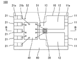
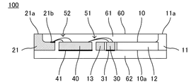
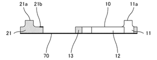
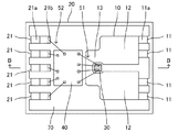
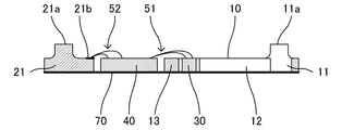
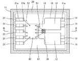
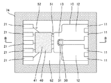
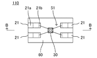
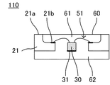
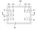
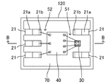
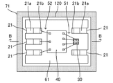
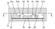
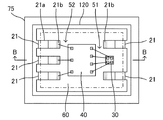
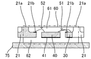
図1A及び図1Bは、本実施形態に係る電流センサ100の構成を示す。ここで、図1Aは、電流センサ100の内部構成を平面視において示し、図1Bは、図1Aにおける基準線BBに関して電流センサ100の断面構成を示す。なお、図1Aにおける上下方向を縦方向、図1A及び図1Bにおける左右方向を横方向、及び図1Bにおける上下方向を高さ方向とする。また、図1A及び図1B並びにこれらに対応するその他の図において、パッケージ60(第1及び第2封止部材61,62)を透過して電流センサ100の内部構成を表している。電流センサ100は、絶縁耐性の高い電流センサを提供することを目的とする電流検出装置の一例であり、導体10、複数のデバイス端子21、磁気センサ30、信号処理IC40、ワイヤ51,52、及びパッケージ60を備える。
導体10は、電流センサ100により検出される電流(被測定電流と呼ぶ)が電流経路に沿って流れる導電性部材である。導体10は、大きな被測定電流を流すために、例えば銅のような金属等の導電体を用いて0.2mm厚、ただし端子部11は0.4mm厚で、横方向右側に設けられる2組の端子部11のうちの一方の組から後述するパッケージ60の内部を通って他方の組に戻る形状に成形される。導体10は、2組の端子部11、2つの脚部12、及び曲部13を含む。
2組の端子部11は、被測定電流を入出力する電流端子であり、横方向右側に縦方向に離間して配設されている。2組の端子部11は、平面視において略矩形状を有し、2組の端子部11に含まれる各2つの端子部11が、それぞれの基端(すなわち、左端)の厚みを絞ってそれぞれ2つの脚部12の右端に一体的に接続する。なお、各組の端子部11は、2つの端子部11に限らず、3以上の端子部11を含んでもよい。
2つの脚部12は、2組の端子部11のうちの一方の組の端子部11に入力された電流を曲部13に送る又は曲部13から他方の組の端子部11に電流を送る部材であり、2組の端子部11の左側に、縦方向に離間して配設されている。2つの脚部12は、平面視において横方向を長手とする矩形状を有し、それぞれ、右端に接続する2組の端子部11をそれぞれ曲部13の2つの端部に一体的に接続する。
曲部13は、2つの脚部12の一方から流れ込む電流の向きを逆向きに変えて他方の脚部12に送り出す部材であり、2つの脚部12の左側に配設されている。曲部13は、平面視において胴部とこれを間に連ねる2つの端部を有してU字状に成形され、胴部を左側に向けて、2つの端部をそれぞれ2つの脚部12に一体的に接続する。ここで、曲部13の内側に形成される空間の幅は、磁気センサ30の幅より大きい。
なお、導体10の底面10aを粗面加工してもよい。ここで、粗面加工された底面10aの算術平均粗さ(Ra)は0.01μm以上とする。それにより、導体10を封止するパッケージ60が導体10の底面10aに密着し、界面の形成が抑止される。
なお、導体10の肉厚部(すなわち、端子部11)の上面11aを除いて薄肉部(すなわち、脚部12及び曲部13)の上面に例えば銀を用いてメッキ膜を設けてもよい。
導体10は、2組の端子部11にそれぞれ含まれる端子部11の上面及び先端面(すなわち、右端面)をパッケージ60の上面及び右側面に面一に露出して、パッケージ60内に封止されている。端子部11の上面11aは、電流センサ100を例えば外部基板上に実装した際に、外部基板上に配設された配線等に接合される。被測定電流は、縦方向の上側(又は下側)の一方の組の端子部11から入力され、上側(又は下側)の脚部12を介して曲部13を流れることでその向きを左向きから右向きに180度を変え、下側(又は上側)の脚部12を介して下側(又は上側)の他方の組の端子部11から出力される。なお、被測定電流が導体10内を流れる経路を電流経路と呼ぶ。
複数のデバイス端子21は、信号処理IC40から出力される電流量の算出結果を外部デバイスに出力する、また補正パラメータを設定するための信号を外部デバイスから信号処理IC40に入力する信号端子である。複数のデバイス端子21は、一例として5つの端子を含み、横方向左側に縦方向に離間して配設されている。複数のデバイス端子21のそれぞれは、例えば銅のような金属等の導電体を用いて0.2mm厚、ただし左端部は0.4mm厚で、横方向を長手とする矩形状に成形される。
なお、複数のデバイス端子21の肉厚部(すなわち、左端部)の上面21aを除いて薄肉部の上面に例えば銀を用いてメッキ膜を設けてもよい。
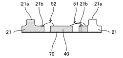
複数のデバイス端子21は、左端部の上面21a及び先端面(すなわち、左端面)をパッケージ60の上面及び左側面に面一に露出して、パッケージ60内に封止されている。デバイス端子21の上面21aは、電流センサ100を例えば外部基板上に実装した際に、外部基板上に配設された配線等に接合される。
磁気センサ30は、導体10に流れる電流により発生する磁場を検出する磁気検出素子の一例である。磁気センサ30として、例えば、InAs、GaAs等から構成される化合物半導体ホール素子、シリコンから構成されるホール素子(或いは増幅回路と一体化されたホールIC)、及び磁気抵抗素子を採用することができる。磁気センサ30は、導体10の曲部13の内側、好ましくは曲部13内における電流経路の曲率中心に配置される。それにより、曲部13に流れる電流により発生する磁場が磁気センサ30に集束し、磁気センサ30により高いSN比で磁場を検出することが可能となる。さらにより高いSN比で地場を検出するには、磁気センサ30の厚さは、導体10の厚さより薄い方が好ましい。
なお、磁気センサ30の底面に絶縁部材31を設けてもよい。絶縁部材31は、粗面加工されたものでもよく、その算術平均粗さ(Ra)は0.01μm以上とする。絶縁部材31として、例えば、ウエハをダイシングして、ウエハ上に形成された磁気センサ30の回路素子を個片化する際に、ウエハの裏面に貼り付けられるダイアタッチフィルムを採用することができる。絶縁部材31により磁気センサ30の底面が(例えば、後述するウェットブラスト時において)保護され、また絶縁部材31が0.01μm以上の算術平均粗さ(Ra)で粗面加工されていることで、パッケージ60が磁気センサ30の底面に密着してこれを封止することにより界面の形成が抑止される。プラズマ処理等の磁気センサ30の底面に大きなダメージが無い方法であり、保護する必要がない場合は、絶縁部材31は無くてもよい。
なお、磁気センサ30の上側、下側、又は両側に磁性体メッキにより形成された磁性体を設け、それらにより磁場を集束して磁気センサ30に入力することとしてもよい。また、磁気センサ30の上面、下面、又は両面を、例えばアルミニウム等の非磁性導体を用いて静電シールドして、パッケージ60外から来る静電ノイズを遮蔽してもよい。
なお、磁気センサ30に入力する外部磁場等にともなうノイズを除くために、導体10の曲部13の外側に外部磁場を検出するための追加の磁気センサを設けてもよい。斯かる場合、信号処理IC40により磁気センサ30の検出信号と追加の磁気センサの検出信号との差分を算出することで、磁気センサ30の検出信号に含まれる外部磁場等に由来するノイズを相殺することができる。
磁気センサ30は、ワイヤボンディングによって信号処理IC40に接続され、検出した磁場の強度に応じた電圧を出力信号として信号処理IC40に出力する。
信号処理IC40は、磁気センサ30が出力する信号を処理して、導体10に流れる電流の量を算出するデバイスである。信号処理IC40は、メモリ、感度補正回路、出力のオフセットを補正するオフセット補正回路、磁気センサ30からの出力信号を増幅する増幅回路、及び温度に応じて出力を補正する温度補正回路等の少なくとも1つを内蔵してもよい。本実施形態では、信号処理IC40は、磁気センサ30と別個のデバイスとしてハイブリッド構成されたものを採用する。信号処理IC40は、導体10の曲部13と複数のデバイス端子21との間に配置される。
なお、信号処理IC40の底面に絶縁部材41を設けてもよい。絶縁部材41は、粗面加工されたものでもよく、その算術平均粗さ(Ra)は0.01μm以上とする。絶縁部材41として、例えば、ウエハをダイシングして、ウエハ上に形成された信号処理IC40の回路素子を個片化する際に、ウエハの裏面に貼り付けられるダイアタッチフィルムを採用することができる。絶縁部材41により信号処理IC40の底面が(例えば、後述するウェットブラスト時において)保護され、また絶縁部材41が0.01μm以上の算術平均粗さ(Ra)で粗面加工されていることで、パッケージ60が信号処理IC40の底面に密着してこれを封止することにより界面の形成が抑止される。
なお、本実施形態においては、信号処理IC40がリードフレーム等によって支持されていない形態を示しているが、信号処理IC40は例えばリードフレーム上に載置されてもよい。また絶縁部材41は、前述のように無くてもよい。
信号処理IC40は、ワイヤボンディングによって複数のデバイス端子21に接続され、それらを介して導体10に流れる電流の量の算出結果を出力する、さらにパラメータの設定等を入力する。なお、複数のデバイス端子21のいずれかをグランド端子として使用してもよい。また、信号処理IC40の上面、下面、又は両面を、例えばアルミニウム等の非磁性導体を用いて静電シールドして、パッケージ60外から来る静電ノイズを遮蔽してもよい。
なお、本実施形態に係る電流センサ100では、磁気センサ30と別個のデバイスとしてハイブリッド構成された信号処理IC40を採用したが、これに代えて、磁気センサ30と同一の半導体基板上に形成された信号処理回路を備える信号処理IC、すなわち磁気センサ30とともにモノリシック構成された信号処理ICを採用してもよい。斯かる場合、導体10の曲部13を同一の半導体基板の上方又は下方にクリアランスを設けて配置し、平面視において導体10の曲部13の内側に同一の半導体基板上の磁気センサ30を位置決めし、パッケージ60により同一の半導体基板を導体10から離間するとともに全ての外面を覆って封止する。また、磁気センサ30と信号処理IC40とが同一の回路基板上にマウントされた、ハイブリッド型の信号処理ICを採用しても良い。
ワイヤ51,52は、例えば銅や金のような金属等の導電体を用いて成形された線状部材である。ワイヤ51は、磁気センサ30及び信号処理IC40の間に架設される4つのワイヤを含み、これらを介して磁気センサ30を駆動し、その検出信号を信号処理IC40に送る。ワイヤ52は、信号処理IC40及び複数のデバイス端子21の上面21bの間に架設される5つのワイヤを含み、これらを介して信号処理IC40の算出結果を出力する。
パッケージ60は、複数のデバイス端子21及び導体10の一部を除いて電流センサ100の構成各部を封止して、保護する封止部材の一例である。ここで、パッケージ60は、磁気センサ30及び信号処理IC40のそれぞれを導体10及び複数のデバイス端子21から離間してそれらとともにそれぞれの外面全面を覆って内部に封止し、それにより導体10と複数のデバイス端子21とを絶縁する。磁気センサ30(信号処理IC40と同一の回路基板上にマウントされている場合の信号処理IC及び回路基板など、磁気センサ30に接する部材も含むものとする)は、例えば導体10及びデバイス端子21と接するように配置された基板、フィルム等に接して支持されることなく、全ての外面がパッケージ60により覆われて封止される。ここで、「全ての外面」とは、磁気センサ30を信号処理IC40と接続するためのボンディングワイヤ等の導体の接続部分を除く外面の全てがパッケージ60で覆われていることをいう。また、磁気センサ31の底面に絶縁部材31が備えられている場合には、絶縁部材31の表面を磁気センサ31の外面とする。
パッケージ60は、例えば、エポキシなどの絶縁性に優れた樹脂を用いてモールド成形することで、矩形状の上面及び上面の一辺の長さより小さい厚さを有する直方体状に成形される。導体10及び複数のデバイス端子21から離間して磁気センサ30及び信号処理IC40をパッケージ60の内部に埋め込んだことで、すなわちそれら単体で埋め込んだことで、パッケージ60に磁気センサ30及び信号処理IC40のそれぞれとの境から拡がり得る界面が形成されないため、高い耐圧を得ることができる。また、磁気センサ30及び信号処理IC40を支持するリードフレームが不要となることで、電流センサ100の小型化が可能となる。また、導体10を半抜き等による段差加工を施して磁気センサ30を囲む曲部13を磁気センサ30を支持するフレームに対して上げる又は下げる必要がないことで、段差加工による導体10の抵抗の増大を避けることができる。
パッケージ60は、導体10、複数のデバイス端子21、磁気センサ30、及び信号処理IC40の少なくとも上面を含む上面側及び少なくとも底面を含む底面側をそれぞれ封止する第1及び第2封止部材61,62を含む。なお、導体10、複数のデバイス端子21、磁気センサ30、及び信号処理IC40の上面に加えてそれらの側面を含んで上面側としてもよく、斯かる場合、底面側に側面は含まないこととする。また、導体10、複数のデバイス端子21、磁気センサ30、及び信号処理IC40の上面のみを含んで上面側としてもよく、斯かる場合、底面側に側面を含むこととする。また、導体10、複数のデバイス端子21、磁気センサ30、及び信号処理IC40の上面に加えてそれらの側面の一部を含んで上面側としてもよく、斯かる場合、底面側に側面の残りの部分を含むこととする。
後述するように、導体10、複数のデバイス端子21、磁気センサ30、及び信号処理IC40の底面を支持してそれらの上面側を第1封止部材61により覆い、導体10、磁気センサ30、及び信号処理IC40の上下を返して、第1封止部材61により覆われた上面側を除くそれらの底面側を第2封止部材62により覆うことで、磁気センサ30及び信号処理IC40を導体10及び複数のデバイス端子21から離間するとともにそれらの外面全面を覆ってパッケージ60内に単体で埋め込み、封止することができる。なお、第1及び第2封止部材61,62は、同一材料が好ましいが、それぞれ異なる材料を用いて形成してもよい。また、第1及び第2封止部材61,62の少なくとも一方は、無機物の材料であるフィラーを含む材料によって形成されていても良い。
本実施形態に係る電流センサ100によれば、パッケージ60により、被測定電流が流れる導体10の曲部13とともに、導体10を流れる電流により発生する磁場を検出する磁気センサ30及び磁気センサ30からの出力信号を処理する信号処理IC40を導体10及び複数のデバイス端子21から離間するとともにそれらの外面全面を覆って封止することで、磁気センサ30及び信号処理IC40を内部に埋め込んだパッケージ60にそれらとの境から拡がり得る界面が形成されないため高い耐圧を得ることができる。
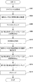
本実施形態に係る電流センサ100の製造方法について説明する。図2に、本実施形態に係る電流センサの製造工程のフローを示す。
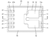
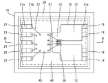
ステップS102では、導体10及び複数のデバイス端子21のパターンを含むリードフレーム20を形成する。図3A及び図3Bに示すように、リードフレーム20は、矩形状の金属フレームであり、その内側に、導体10のパターンをその2組の端子部11をフレームの右枠に接続し、複数のデバイス端子21のパターンをそれらの左端部をフレームの左枠に接続して含む。
なお、本実施形態では、1つのリードフレーム20に1つの電流センサ100を構成する一組の導体10及び複数のデバイス端子21のパターンのみを含むとしたが、これは説明のための一例であり、1つのリードフレーム20に複数の電流センサ100を構成する複数組の導体10及び複数のデバイス端子21が配列されたパターンを含んでもよい。
まず、例えば一枚の金属板をプレス加工することにより、リードフレーム20の原型を形成する。ここで、金属板は、例えば0.4mm厚を有する。次に、導体10の端子部11に対応するパターン部分の上面11a及び複数のデバイス端子21の左端部に対応するパターン部分の上面21aを除いてリードフレーム20の原型をエッチングすることにより、例えば0.2mm厚で薄肉に成形する。これにより、肉厚の導体10の端子部11及び複数のデバイス端子21の左端部が接続端子として機能する。次に、エッチングにより薄肉化された部分の上面に例えば銀を用いてメッキ膜を設ける。なお、これに代えて、リードフレーム20の上面全体にメッキ膜を設け、後述する第1及び第2封止部材61,62の硬化後に導体10の端子部11の上面11a及び複数のデバイス端子21の左端部の上面21a上のメッキ膜を除去し、例えば錫を用いて新しいメッキ膜を設けてもよい。最後に、リードフレーム20の下面にシート状の支持部材70の外縁を貼り付けて、フレーム内側に底面を設ける。支持部材70として、例えば、粘着層が形成された耐熱性の高いポリイミドテープ、セラミックシート等を採用することができる。
なお、本実施形態に係る電流センサ100の製造方法では、リードフレーム20の原型をエッチングすることにより、接続端子として機能する導体10の端子部11及び複数のデバイス端子21の左端部を形成したが、これに代えて、例えばリードフレーム20を曲げ加工又は半抜き加工することで、導体10の脚部12、曲部13、複数のデバイス端子21の右端部を含むリードフレーム20の内部パターンに対して導体10の端子部11及び複数のデバイス端子21の左端部を含むリードフレーム20の外部パターンを曲げる又は上げることで接続端子を形成してもよい。ここで、曲げ加工する場合、リードフレーム20は例えば0.2mm厚を有するとし、半抜き加工する場合、リードフレーム20は例えば0.3mm厚を有し、0.12〜0.15mmを半抜きすることとする。また、リードレスのパッケージ構造を例にしたが、第1封止部材61又は第2封止部材62の外部でリードフレームが曲げられたリードを有するパッケージ構造としてもよい。
ステップS104では、リードフレーム20の内側に磁気センサ30及び信号処理IC40をリードフレーム20から離間して設置する。図4A及び図4Bに示すように、リードフレーム20の底面として設けられた支持部材70上で、磁気センサ30を、平面視において導体10の曲部13の内側、好ましくは曲部13内における電流経路の曲率中心に曲部13から離間して配置し、信号処理IC40を、平面視において、導体10の曲部13と複数のデバイス端子21との間にそれぞれから離間して配置する。なお、磁気センサ30及び信号処理IC40は、支持部材70の表面に形成された粘着層により固着される。
ステップS106では、図4A及び図4Bに示すように、ワイヤ51により磁気センサ30及び信号処理IC40をワイヤボンディングし、ワイヤ52により信号処理IC40及び複数のデバイス端子21をワイヤボンディングする。
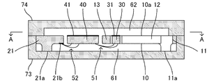
ステップS108では、リードフレーム20、磁気センサ30、及び信号処理IC40の少なくとも上面を含む上面側(本例では上面に加えて側面を含むが、上面のみを含む又は上面に加えて側面の一部を含んでもよい)を第1封止部材61により封止する。図5A及び図5Bに示すように、磁気センサ30及び信号処理IC40が支持部材70上に配置されたリードフレーム20を上面が開いた箱体状の型枠71内に収容し、板状の蓋体72を型枠71上に押しつけてリードフレーム20を含む型枠71の内部空間を閉じ、型枠71の貫通孔(不図示)を介して封止部材を型枠71内に流し込む。ここで、第1封止部材61として、絶縁性材料であるエポキシなどの樹脂を採用することができる。また、第1封止部材61として、フィラーを含む樹脂を採用してもよい。さらに、導体10の端子部11の上面11a及びデバイス端子21の上面21aへの樹脂滲みを防止するために、蓋体72の型枠71側の面を樹脂フィルム(例えば、テフロン(登録商標)フィルム)で覆ってもよい。
ステップS110では、リードフレーム20から支持部材70を除去する。第1封止部材61により上面側が封止されたリードフレーム20を型枠71から取り出し、上下を返して、リードフレーム20の下面から支持部材70を剥がす。
ステップS112では、支持部材70が除去されたリードフレーム20(の導体10及び複数のデバイス端子21の部分)、磁気センサ30、信号処理IC40及び第1封止部材61のそれぞれの底面を粗面加工する。ここで、粗面加工の方法として、例えばウェットブラスト処理又はプラズマ処理を採用することができる。ウェットブラスト処理は、微細粒子を水に含めて表面に吹き付けることにより、微細粒子が衝突して表面の表層が削られるとともに水により異物が流し落とされ、例えばサブミクロンのオーダーで表面を加工する。プラズマ処理は、プラズマを表面に照射することで表面を加工する。リードフレーム20(導体10及び複数のデバイス端子21)、磁気センサ30、及び信号処理IC40のそれぞれの底面の算術平均粗さ(Ra)は0.01μm以上とする。それにより、リードフレーム20の底面側を封止する第2封止部材62が、導体10、磁気センサ30、信号処理IC40及び第1封止部材61のそれぞれの底面に密着する。
なお、リードフレーム20、磁気センサ30、及び信号処理IC40を予め粗面加工することとして、ステップS112を省略してもよい。斯かる場合に、少なくとも導体10及び複数のデバイス端子21の部分が粗化メッキされたリードフレーム20を使用してもよい。
なお、導体10、磁気センサ30、信号処理IC40及び第1封止部材61の底面が粗面加工されていなくて第2封止部材62がそれらに十分に密着する場合には、ステップS112を省略してもよい。また、リードフレーム20、磁気センサ30、信号処理IC40の底面を予め粗面加工することとしてステップS112を省略してもよい。
ステップS114では、リードフレーム20、磁気センサ30、及び信号処理IC40の少なくとも底面を含む底面側(本例では底面のみを含むが、ステップS108において上面のみを含む又は上面に加えて側面の一部を含む上面側を第1封止部材61により封止した場合、底面に加えて側面又は側面の残りの部分を含むとする)を第2封止部材62により封止する。ステップS108において成形された第1封止部材61のポストキュアを実施する前に、図6A及び図6Bに示すように、底面が粗面加工されたリードフレーム20を上下を返した状態で上面が開いた箱体状の型枠73内に収容し、底面が開いた箱体状の型枠74を型枠73上に押しつけてリードフレーム20の底面により型枠74の内部空間を閉じ、型枠74の貫通孔(不図示)を介して第2封止部材62を型枠74内に流し込む。ここで、第2封止部材62として、第1封止部材と同じ絶縁性材料であるエポキシなどの樹脂を採用する。また、第2封止部材62として、フィラーを含む樹脂を採用してもよい。それにより、第1封止部材61の樹脂がガラス転移点を超えて柔らかくなっている間に、リードフレーム20に含まれる導体10及び複数のデバイス端子21、磁気センサ30、及び信号処理IC40のそれぞれの底面が第2封止部材62により覆われ、導体10等の底面を覆わない第2封止部材62の境界部分のエポキシ樹脂成分と第1封止部材61の境界部分のエポキシ樹脂成分とが一体化して硬化する。この様な手順で作製することで、後に断面を観察した際に、第2封止部材62中に含まれる無機物の材料であるフィラーで特に20μm以上のサイズのものは、第1封止部材61と第2封止部材62の境界部を跨ぐように存在しないという特徴が観察できる。一体化した第1及び第2封止部材61,62に導体10、複数のデバイス端子21、磁気センサ30、又は信号処理IC40との境から拡がり得る界面が形成されないため高い耐圧を得ることができる。
ステップS116では、第1及び第2封止部材61,62のポストキュアを実施する。それにより、第1及び第2封止部材61,62がそれらの境界部分を一体化してポストキュアすることで未硬化の割合が低減し、パッケージ60をなし、そのパッケージ60により磁気センサ30及び信号処理IC40がリードフレーム20に含まれる導体10及び複数のデバイス端子21から離間して内部に、ただしリードフレーム20のフレーム並びにこれと導体10の端子部11及び複数のデバイス端子21とを連結する部分を残して、封止される。
なお、上述のように第1及び第2封止部材61,62をそれら両方の形成後に同時にポストキュアすることは、第1及び第2封止部材61,62の境界部分が一体化してそれらの間に界面が形成されないことで有効であるが、界面が形成されない又は形成されても無視できる程度であれば、第1封止部材61のポストキュアし、その後に第2封止部材62をポストキュアしてもよい。
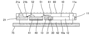
ステップS118では、パッケージ60をダイシングする。図7A及び図7Bに示すように、パッケージ60の上下を返してダイシングテープ75上に貼り付け、パッケージ60から露出するパターン、すなわちリードフレーム20のフレームと導体10の端子部11及び複数のデバイス端子21とを連結する部分を第1封止部材61の外縁とともに切断する。それにより、導体10の端子部11の上面11a及び複数のデバイス端子21の上面21aがパッケージ60の上面から面一に露出して接続端子をなすことで、電流センサ100が完成する。
本実施形態に係る電流センサ100の製造方法によれば、支持部材70上に導体10及び複数のデバイス端子21を含むリードフレーム20、磁気センサ30、及び信号処理IC40を互いに離間して配置し、それぞれの少なくとも上面を含む上面側を第1封止部材61により封止し、支持部材70を除去した後、それぞれの底面を含む上面側以外の底面側を第2封止部材62により封止することで、第1及び第2封止部材61,62が一体化してなるパッケージ60により、被測定電流が流れる導体10の曲部13、導体10に流れる電流により発生する磁場を検出する磁気センサ30、磁気センサ30からの出力信号を処理する信号処理IC40が互いに離間するとともにそれぞれの外面全面を覆って封止され、磁気センサ30及び信号処理IC40を内部に埋め込んだパッケージ60にそれらとの境から拡がり得る界面が形成されないため高い耐圧を得ることができる。
なお、本実施形態に係る電流センサ100では、パッケージ60は、導体10の端子部11及び複数のデバイス端子21にリードを有さないリードレスパッケージとして成形することとしたが、これに代えて、リードを有するパッケージとして成形してもよい。
なお、本実施形態に係る電流センサ100において、導体10に流れる電流は、直流であっても交流であってもよい。また、直流の場合において、通電する電流の向きを任意に定めてよい。
なお、本実施形態に係る電流センサ100の製造方法では、型枠71〜74を用いた樹脂モールド成形によりパッケージ60を形成したが、これに代えて3Dプリンタを用いてパッケージを形成してもよい。
なお、本実施形態に係る電流センサ100は、導体10に電流を流さないで、外部磁場を検出してその強度を測定する磁気検出装置として使用してもよい。斯かる場合、後述する変形例のようにパッケージ60内に導体10を設けなくてもよい。
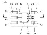
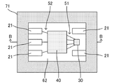
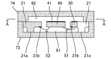
図8A及び図8Bは、変形例に係るホールセンサ110の構成を示す。ここで、図8Aは、ホールセンサ110の内部構成を平面視において示し、図8Bは、図8Aにおける基準線BBに関してホールセンサ110の断面構成を示す。ホールセンサ110は、外部磁場を検出してその強度を測定する磁気検出装置の一例であり、磁気センサ30、複数のデバイス端子21、ワイヤ51、及びパッケージ60を備える。これらの構成各部は、先述の電流センサ100が備えるそれらと同様に構成されてよく、そのため同じ符号を用いて図面中に示すとともに詳細説明を省略することとする。
磁気センサ30は、ホールセンサ110に入る磁場(すなわち、外部磁場)を検出する磁気検出素子の一例である。磁気センサ30は、ホールセンサ110の中央に配置される。磁気センサ30は、ワイヤボンディングによって複数のデバイス端子21に接続され、検出した磁場の強度に応じた電圧を出力信号として、例えば複数のデバイス端子21を介してホールセンサ110に接続される信号処理ICに出力する。
複数のデバイス端子21は、磁気センサ30の出力信号を外部デバイスに出力する。複数のデバイス端子21は、一例として4つの端子を含み、磁気センサ30に対して横方向の両側に各2つの端子が縦方向に離間して配設されている。
ワイヤ51は、磁気センサ30及び複数のデバイス端子21の上面21bの間に架設される4つのワイヤを含み、これらを介して磁気センサ30の検出信号を出力する。
パッケージ60は、複数のデバイス端子21の一部を除いてホールセンサ110の構成各部を封止して保護する。パッケージ60は、磁気センサ30を複数のデバイス端子21から離間してそれらとともにその外面全面を覆って内部に封止し、それにより複数のデバイス端子21のそれぞれから絶縁する。つまり、磁気センサ30は、例えばデバイス端子21と接するように配置された基板、フィルム等に接して支持されることなく、外面全面がパッケージ60により覆われて封止される。パッケージ60により、その内部に磁気センサ30を複数のデバイス端子21から離間して埋め込んだことで、すなわちそれら単体で埋め込んだことで、パッケージ60に磁気センサ30の境から拡がり得る界面が形成されないため、高い耐圧を得ることができる。また、磁気センサ30を支持するリードフレームが不要となることで、ホールセンサ110の小型化が可能となる。
パッケージ60は、複数のデバイス端子21及び磁気センサ30の少なくとも上面を含む上面側及び少なくとも底面を含む底面側をそれぞれ封止する第1及び第2封止部材61,62を含む。先述の電流センサ100と同様に、複数のデバイス端子21及び磁気センサ30の底面を支持してそれらの上面側を第1封止部材61により覆い、磁気センサ30の上下を返してそれらの底面側を第2封止部材62により覆うことで、磁気センサ30を複数のデバイス端子21から離間するとともにそれらの外面全面を覆ってパッケージ60内に単体で埋め込み、封止することができる。なお、第1及び第2封止部材61,62は、同一材料が好ましいが、それぞれ異なる材料を用いて形成してもよい。
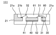
図9A及び図9Bは、変形例に係るホールIC111の構成を示す。ここで、図9Aは、ホールIC111の内部構成を平面視において示し、図9Bは、図9Aにおける基準線BBに関してホールIC111の断面構成を示す。ホールIC111は、外部磁場を検出してその強度を測定する磁気検出装置の一例であり、複数のデバイス端子21、磁気センサ30、信号処理IC40、ワイヤ51,52、及びパッケージ60を備える。これらの構成各部は、先述の電流センサ100が備えるそれらと同様に構成されてよく、そのため同じ符号を用いて図面中に示すとともに詳細説明を省略することとする。
磁気センサ30は、ホールIC111に入る磁場(すなわち、外部磁場)を検出する磁気検出素子の一例である。磁気センサ30は、ホールIC111の中央右側に配置される。磁気センサ30は、ワイヤボンディングによって信号処理IC40に接続され、検出した磁場の強度に応じた電圧を出力信号として信号処理IC40に出力する。
信号処理IC40は、磁気センサ30が出力する信号を処理して、ホールIC111に入る磁場の強度を算出する。変形例では、信号処理IC40は、磁気センサ30と別個のデバイスとしてハイブリッド構成されたものを採用する。信号処理IC40は、ホールIC111の中央に磁気センサ30と隣接して配置される。信号処理IC40は、ワイヤボンディングによって複数のデバイス端子21に接続され、それらを介して磁場の強度の算出結果を出力する、さらにパラメータの設定等を入力する。なお、複数のデバイス端子21のいずれかをグランド端子として使用してもよい。
なお、変形例に係るホールIC111では、磁気センサ30と別個のデバイスとしてハイブリッド構成された信号処理IC40を採用したが、これに代えて、磁気センサ30と同一の半導体基板上に形成された信号処理回路を備える信号処理IC、すなわち磁気センサ30とともにモノリシック構成された信号処理ICを採用してもよい。また、磁気センサ30と信号処理IC40とが同一の回路基板上にマウントされた、ハイブリッド型の信号処理ICを採用しても良い。
複数のデバイス端子21は、信号処理IC40から出力される磁場の強度の算出結果を外部デバイスに出力する、また補正パラメータを設定するための信号を外部デバイスから信号処理IC40に入力する。複数のデバイス端子21は、一例として5つの端子を含み、横方向左側に3つの端子が縦方向に離間して、横方向右側に2つの端子が磁気センサ30を間に挟んで縦方向に離間して、それぞれ配設されている。
ワイヤ51は、磁気センサ30及び信号処理IC40の間に架設される4つのワイヤを含み、これらを介して磁気センサ30を駆動し、その検出信号を信号処理IC40に送る。ワイヤ52は、信号処理IC40及び複数のデバイス端子21の上面21bの間に架設される3つのワイヤを含み、これらを介して信号処理IC40の算出結果を出力する。
パッケージ60は、複数のデバイス端子21の一部を除いてホールIC111の構成各部を封止して保護する。パッケージ60は、磁気センサ30及び信号処理IC40のそれぞれを複数のデバイス端子21から離間してそれらとともにそれぞれの外面全面を覆って内部に封止し、それにより複数のデバイス端子21のそれぞれから絶縁する。つまり、磁気センサ30(信号処理IC40と同一の回路基板上にマウントされている場合の信号処理IC及び回路基板など、磁気センサ30に接する部材も含むものとする)は、例えばデバイス端子21と接するように配置された基板、フィルム等に接して支持されることなく、外面全面がパッケージ60により覆われて封止される。パッケージ60により、その内部に磁気センサ30を複数のデバイス端子21から離間して埋め込んだことで、すなわちそれら単体で埋め込んだことで、パッケージ60に磁気センサ30の境から拡がり得る界面が形成されないため、高い耐圧を得ることができる。また、磁気センサ30を支持するリードフレームが不要となることで、ホールIC111の小型化が可能となる。
パッケージ60は、複数のデバイス端子21、磁気センサ30、及び信号処理IC40の少なくとも上面を含む上面側及び少なくとも底面を含む底面側をそれぞれ封止する第1及び第2封止部材61,62を含む。複数のデバイス端子21、磁気センサ30、及び信号処理IC40の底面を支持してそれらの上面側を第1封止部材61により覆い、磁気センサ30、及び信号処理IC40の上下を返してそれらの底面側を第2封止部材62により覆うことで、磁気センサ30及び信号処理IC40を複数のデバイス端子21から離間するとともにそれらの外面全面を覆ってパッケージ60内に単体で埋め込み、封止することができる。なお、第1及び第2封止部材61,62は、同一材料が好ましいが、それぞれ異なる材料を用いて形成してもよい。
変形例に係るホールIC111の製造方法について説明する。図10に、変形例に係るホールIC111の製造工程のフローを示す。
ステップS202では、複数のデバイス端子21のパターンを含むリードフレーム120を形成する。図11A及び図11Bに示すように、リードフレーム120は、矩形状の金属フレームであり、その内側に、複数のデバイス端子21のうちの3つのパターンをそれらの左端部をフレームの左枠に接続し、2つのパターンをそれらの右端部をフレームの右枠に接続して含み、シート状の支持部材70をその外縁をリードフレーム120の下面に貼り付けてその底面として含む。リードフレーム120の製造方法は、先述のリードフレーム20と同様である。
ステップS204では、リードフレーム120の内側に磁気センサ30及び信号処理IC40をリードフレーム120から離間して設置する。図12A及び図12Bに示すように、リードフレーム120の底面として設けられた支持部材70上で、磁気センサ30を平面視においてリードフレーム120の中央右側に、信号処理IC40を平面視においてリードフレーム120の中央に、複数のデバイス端子21から離間して配置する。なお、磁気センサ30及び信号処理IC40は、支持部材70の表面に形成された粘着層により固着される。
ステップS206では、図12A及び図12Bに示すように、ワイヤ51により磁気センサ30及び信号処理IC40をワイヤボンディングし、ワイヤ52により信号処理IC40及び複数のデバイス端子21をワイヤボンディングする。
ステップS208では、リードフレーム120、磁気センサ30、及び信号処理IC40の少なくとも上面を含む上面側(本例では上面に加えて側面を含むが、上面のみを含む又は上面に加えて側面の一部を含んでもよい)を第1封止部材61により封止する。図13A及び図13Bに示すように、磁気センサ30及び信号処理IC40が支持部材70上に配置されたリードフレーム120を上面が開いた箱体状の型枠71内に収容し、板状の蓋体72を型枠71上に押しつけてリードフレーム120を含む型枠71の内部空間を閉じ、型枠71の貫通孔(不図示)を介して封止部材を型枠71内に流し込む。ここで、第1封止部材61として、エポキシなどの樹脂を採用することができる。また、第1封止部材61として、フィラーを含む樹脂を採用してもよい。さらに、デバイス端子21の上面21aへの樹脂滲みを防止するために、蓋体72の型枠71側の面を樹脂フィルム(例えば、テフロン(登録商標)フィルム)で覆ってもよい。
ステップS210では、リードフレーム120から支持部材70を除去する。第1封止部材61により上面側が封止されたリードフレーム120を型枠71から取り出し、上下を返して、リードフレーム120の下面から支持部材70を剥がす。
ステップS212では、支持部材70が除去されたリードフレーム120(の複数のデバイス端子21の部分)、磁気センサ30、信号処理IC40及び第1封止部材61のそれぞれの底面を粗面加工する。ここで、粗面加工の方法として、例えばウェットブラスト処理又はプラズマ処理を採用することができる。
ステップS214では、リードフレーム120、磁気センサ30、及び信号処理IC40の少なくとも底面を含む底面側(本例では底面のみを含むが、ステップS208において上面のみを含む又は上面に加えて側面の一部を含む上面側を第1封止部材61により封止した場合、底面に加えて側面又は側面の残りの部分を含むとする)を第2封止部材62により封止する。ステップS208において成形された第1封止部材61のポストキュアを実施する前に、図14A及び図14Bに示すように、底面が粗面加工されたリードフレーム120を上下を返した状態で上面が開いた箱体状の型枠73内に収容し、底面が開いた箱体状の型枠74を型枠73上に押しつけてリードフレーム120の底面により型枠74の内部空間を閉じ、型枠74の貫通孔(不図示)を介して第2封止部材62を型枠74内に流し込む。
ステップS216では、第1及び第2封止部材61,62のポストキュアを実施する。それにより、第1及び第2封止部材61,62がそれらの境界部分を一体化してポストキュアすることで未硬化の割合が低減し、パッケージ60をなし、そのパッケージ60により磁気センサ30及び信号処理IC40がリードフレーム20に含まれる複数のデバイス端子21から離間して内部に、ただしリードフレーム120のフレーム並びにこれと複数のデバイス端子21とを連結する部分を残して、封止される。
ステップS218では、パッケージ60をダイシングする。図15A及び図15Bに示すように、パッケージ60の上下を返してダイシングテープ75上に貼り付け、パッケージ60から露出するパターン、すなわちリードフレーム120のフレームと複数のデバイス端子21とを連結する部分を第1封止部材61の外縁とともに切断する。それにより、複数のデバイス端子21の上面21aがパッケージ60の上面から面一に露出して接続端子をなすことで、ホールIC111が完成する。
変形例に係るホールIC111の製造方法によれば、支持部材70上に複数のデバイス端子21を含むリードフレーム120、磁気センサ30、及び信号処理IC40を互いに離間して配置し、それぞれの少なくとも上面を含む上面側を第1封止部材61により封止し、支持部材70を除去した後、それぞれの底面を含む上面側以外の底面側を第2封止部材62により封止することで、第1及び第2封止部材61,62が一体化してなるパッケージ60により、磁気センサ30、磁気センサ30からの出力信号を処理する信号処理IC40が互いに離間するとともにそれぞれの外面全面を覆って封止され、磁気センサ30及び信号処理IC40を内部に埋め込んだパッケージ60にそれらとの境から拡がり得る界面が形成されないため高い耐圧を得ることができる。
なお、変形例に係るホールセンサ110もホールIC111の製造方法と同様の方法により製造することができる。ただし、ステップS204においてリードフレーム120の内側に信号処理IC40を設置しなくてよく、これに応じてステップS206からS218において信号処理IC40に係る処理を省略してよい。
以上、本発明を実施の形態を用いて説明したが、本発明の技術的範囲は上記実施の形態に記載の範囲には限定されない。上記実施の形態に、多様な変更または改良を加えることが可能であることが当業者に明らかである。その様な変更または改良を加えた形態も本発明の技術的範囲に含まれ得ることが、特許請求の範囲の記載から明らかである。
特許請求の範囲、明細書、および図面中において示した装置、システム、プログラム、および方法における動作、手順、ステップ、および段階等の各処理の実行順序は、特段「より前に」、「先立って」等と明示しておらず、また、前の処理の出力を後の処理で用いるのでない限り、任意の順序で実現しうることに留意すべきである。特許請求の範囲、明細書、および図面中の動作フローに関して、便宜上「まず、」、「次に、」等を用いて説明したとしても、この順で実施することが必須であることを意味するものではない。