JP6971908B2 - A method for manufacturing a magnetic detector, a current detector, a magnetic detector, and a method for manufacturing a current detector. - Google Patents

A method for manufacturing a magnetic detector, a current detector, a magnetic detector, and a method for manufacturing a current detector. Download PDF

Info

Publication number
JP6971908B2
JP6971908B2 JP2018079140A JP2018079140A JP6971908B2 JP 6971908 B2 JP6971908 B2 JP 6971908B2 JP 2018079140 A JP2018079140 A JP 2018079140A JP 2018079140 A JP2018079140 A JP 2018079140A JP 6971908 B2 JP6971908 B2 JP 6971908B2
Authority
JP
Japan
Prior art keywords
magnetic sensor
conductor
sealing member
magnetic
signal processing
Prior art date
Legal status (The legal status is an assumption and is not a legal conclusion. Google has not performed a legal analysis and makes no representation as to the accuracy of the status listed.)
Active
Application number
JP2018079140A
Other languages
Japanese (ja)
Other versions
JP2018179994A (en
Inventor
敏昭 福中
Current Assignee (The listed assignees may be inaccurate. Google has not performed a legal analysis and makes no representation or warranty as to the accuracy of the list.)
Asahi Kasei EMD Corp
Original Assignee
Asahi Kasei EMD Corp
Priority date (The priority date is an assumption and is not a legal conclusion. Google has not performed a legal analysis and makes no representation as to the accuracy of the date listed.)
Filing date
Publication date
Application filed by Asahi Kasei EMD Corp filed Critical Asahi Kasei EMD Corp
Priority to US15/956,744 priority Critical patent/US10698005B2/en
Publication of JP2018179994A publication Critical patent/JP2018179994A/en
Priority to JP2021179785A priority patent/JP2022016475A/en
Application granted granted Critical
Publication of JP6971908B2 publication Critical patent/JP6971908B2/en
Active legal-status Critical Current
Anticipated expiration legal-status Critical

Links

Images

Description

本発明は、磁気検出装置、電流検出装置、磁気検出装置の製造方法、及び電流検出装置の製造方法に関する。 The present invention relates to a magnetic detection device, a current detection device, a method for manufacturing the magnetic detection device, and a method for manufacturing the current detection device.

磁気センサを用いて磁場の強度を検出する磁気検出装置及び電流の量を検出する電流検出装置(電流センサとも呼ぶ)が知られている。例えば特許文献1には、被測定電流が入力される1次導体、信号処理ICを支持する2次導体、2次導体の2つの張り出し部の間に架けられた絶縁テープ上に支持して、平面視において1次導体のギャップに配置された磁気センサ、及びこれらの構成各部を封止するパッケージを有する電流センサが開示されている。電流センサは、1次導体に電流が入力されると、その電流により1次導体の周囲に発生する磁場を磁気センサを用いて検出して、電流の量に応じた出力信号を出力する。
特許文献1 国際公開第2015/015539号
A magnetic detection device that detects the strength of a magnetic field using a magnetic sensor and a current detection device (also called a current sensor) that detects the amount of current are known. For example, in Patent Document 1, a primary conductor into which a measured current is input, a secondary conductor supporting a signal processing IC, and an insulating tape laid between two overhanging portions of the secondary conductor are supported. A magnetic sensor arranged in a gap of a primary conductor in plan view and a current sensor having a package for sealing each of these components are disclosed. When a current is input to the primary conductor, the current sensor detects the magnetic field generated around the primary conductor by the current using a magnetic sensor, and outputs an output signal according to the amount of the current.
Patent Document 1 International Publication No. 2015/015539

斯かる構成の電流検出装置及び磁気検出装置において、高い絶縁耐性が求められる。 High dielectric strength is required in the current detection device and the magnetic detection device having such a configuration.

本発明の第1の態様においては、磁場を検出する磁気センサと、磁気センサの全ての外面を覆って封止する封止部材と、を備える磁気検出装置が提供される。 In the first aspect of the present invention, there is provided a magnetic detection device including a magnetic sensor that detects a magnetic field and a sealing member that covers and seals the entire outer surface of the magnetic sensor.

本発明の第2の態様においては、第1の態様の磁気検出装置と、被測定電流が流れる導体と、を備え、磁気センサは、導体に流れる電流により発生する磁場を検出し、封止部材は、導体の少なくとも一部を封止して磁気センサを導体から離間する、電流検出装置が提供される。 In the second aspect of the present invention, the magnetic detection device of the first aspect and the conductor through which the measured current flows are provided, and the magnetic sensor detects the magnetic field generated by the current flowing through the conductor and is a sealing member. Provides a current detector that seals at least a portion of the conductor and separates the magnetic sensor from the conductor.

本発明の第3の態様においては、粗面加工された底面を有する、被測定電流が流れる導体と、導体に流れる電流により発生する磁場を検出する磁気センサと、導体の少なくとも一部及び磁気センサを封止する封止部材と、を備える電流検出装置が提供される。 In the third aspect of the present invention, a conductor having a roughened bottom surface through which a measured current flows, a magnetic sensor for detecting a magnetic field generated by the current flowing through the conductor, and at least a part of the conductor and a magnetic sensor. A current detecting device comprising a sealing member for sealing the magnet is provided.

本発明の第4の態様においては、支持部材上に、磁場を検出する磁気センサを配置する段階と、磁気センサの上面を第1封止部材により封止する段階と、支持部材を除去する段階と、磁気センサの底面を第2封止部材により封止する段階と、を備える磁気検出装置の製造方法が提供される。 In the fourth aspect of the present invention, a step of arranging a magnetic sensor for detecting a magnetic field on a support member, a step of sealing the upper surface of the magnetic sensor with a first sealing member, and a step of removing the support member. And a step of sealing the bottom surface of the magnetic sensor with a second sealing member are provided.

本発明の第5の態様においては、支持部材上に、被測定電流が流れる導体及び導体に流れる電流により発生する磁場を検出する磁気センサを互いに離間して配置する段階と、導体の少なくとも一部及び磁気センサの上面を第1封止部材により封止する段階と、支持部材を除去する段階と、導体の少なくとも一部及び磁気センサの底面を第2封止部材により封止する段階と、を備える電流検出装置の製造方法が提供される。 In the fifth aspect of the present invention, a stage in which a conductor through which a measured current flows and a magnetic sensor for detecting a magnetic field generated by the current flowing through the conductor are arranged apart from each other on a support member, and at least a part of the conductor. The step of sealing the upper surface of the magnetic sensor with the first sealing member, the step of removing the support member, and the step of sealing at least a part of the conductor and the bottom surface of the magnetic sensor with the second sealing member. A method for manufacturing a current detector is provided.

なお、上記の発明の概要は、本発明の特徴の全てを列挙したものではない。また、これらの特徴群のサブコンビネーションもまた、発明となりうる。 The outline of the above invention does not list all the features of the present invention. A subcombination of these feature groups can also be an invention.

本実施形態に係る電流センサの内部構成を示す。The internal configuration of the current sensor according to this embodiment is shown. 図1Aにおける基準線BBに関する電流センサの断面構成を示す。FIG. 1A shows a cross-sectional configuration of a current sensor with respect to the reference line BB. 本実施形態に係る電流センサの製造工程のフローを示す。The flow of the manufacturing process of the current sensor which concerns on this embodiment is shown. 電流センサの製造工程の一ステップにより形成された電流センサの状態、すなわち下面に支持部材が貼り付けられたリードフレームの構成を示す。The state of the current sensor formed by one step of the current sensor manufacturing process, that is, the configuration of the lead frame in which the support member is attached to the lower surface is shown. 図3Aにおける基準線BBに関する電流センサの断面を示す。FIG. 3A shows a cross section of the current sensor with respect to the reference line BB. 電流センサの製造工程の一ステップにより形成された電流センサの状態、すなわち支持部材上に磁気センサ及び信号処理ICが互いに離間して配置され、信号処理ICが磁気センサ及び端子にワイヤボンディングされた状態を示す。The state of the current sensor formed by one step of the current sensor manufacturing process, that is, the state in which the magnetic sensor and the signal processing IC are arranged apart from each other on the support member, and the signal processing IC is wire-bonded to the magnetic sensor and the terminal. Is shown. 図4Aにおける基準線BBに関する電流センサの断面を示す。FIG. 4A shows a cross section of the current sensor with respect to the reference line BB. 電流センサの製造工程の一ステップにより形成された電流センサの状態、すなわちリードフレーム、磁気センサ、及び信号処理ICの上面側が第1封止部材により封止された状態を図5Bにおける基準線AAについて示す。The state of the current sensor formed by one step of the current sensor manufacturing process, that is, the state in which the lead frame, the magnetic sensor, and the upper surface side of the signal processing IC are sealed by the first sealing member is the reference line AA in FIG. 5B. show. 図5Aにおける基準線BBに関する電流センサの断面を示す。FIG. 5A shows a cross section of the current sensor with respect to the reference line BB. 電流センサの製造工程の一ステップにより形成された電流センサの状態、すなわち支持部材が除去されたリードフレーム、磁気センサ、及び信号処理ICの底面側が第2封止部材により封止された状態を図6Bにおける基準線AAについて示す。The state of the current sensor formed by one step of the manufacturing process of the current sensor, that is, the state where the lead frame from which the support member is removed, the magnetic sensor, and the bottom surface side of the signal processing IC are sealed by the second sealing member is shown. The reference line AA in 6B is shown. 図6Aにおける基準線BBに関する電流センサの断面を示す。FIG. 6A shows a cross section of the current sensor with respect to the reference line BB. 電流センサの製造工程の一ステップにより形成された電流センサの状態、すなわちリードフレーム、磁気センサ、及び信号処理ICが封止部材によりパッケージされた状態を示す。The state of the current sensor formed by one step of the current sensor manufacturing process, that is, the state in which the lead frame, the magnetic sensor, and the signal processing IC are packaged by the sealing member is shown. 図7Aにおける基準線BBに関する電流センサの断面を示す。FIG. 7A shows a cross section of the current sensor with respect to the reference line BB. 変形例に係るホールセンサの内部構成を示す。The internal configuration of the Hall sensor according to the modified example is shown. 図8Aにおける基準線BBに関するホールセンサの断面構成を示す。FIG. 8A shows a cross-sectional configuration of the Hall sensor with respect to the reference line BB. 変形例に係るホールICの内部構成を示す。The internal configuration of the Hall IC according to the modified example is shown. 図9Aにおける基準線BBに関するホールICの断面構成を示す。The cross-sectional structure of the Hall IC with respect to the reference line BB in FIG. 9A is shown. 変形例に係るホールICの製造工程のフローを示す。The flow of the manufacturing process of the Hall IC which concerns on a modification is shown. ホールICの製造工程の一ステップにより形成されたホールICの状態、すなわち下面に支持部材が貼り付けられたリードフレームの構成を示す。The state of the Hall IC formed by one step of the Hall IC manufacturing process, that is, the configuration of the lead frame in which the support member is attached to the lower surface is shown. 図11Aにおける基準線BBに関するホールICの断面を示す。FIG. 11A shows a cross section of the Hall IC with respect to the reference line BB. ホールICの製造工程の一ステップにより形成されたホールICの状態、すなわち支持部材上に磁気センサ及び信号処理ICが互いに離間して配置され、信号処理ICが磁気センサ及び端子にワイヤボンディングされた状態を示す。The state of the Hall IC formed by one step of the Hall IC manufacturing process, that is, the state in which the magnetic sensor and the signal processing IC are arranged apart from each other on the support member, and the signal processing IC is wire-bonded to the magnetic sensor and the terminal. Is shown. 図12Aにおける基準線BBに関するホールICの断面を示す。FIG. 12A shows a cross section of the Hall IC with respect to the reference line BB. ホールICの製造工程の一ステップにより形成されたホールICの状態、すなわちリードフレーム、磁気センサ、及び信号処理ICの上面側が第1封止部材により封止された状態を図13Bにおける基準線AAについて示す。Regarding the reference line AA in FIG. 13B, the state of the Hall IC formed by one step of the Hall IC manufacturing process, that is, the state in which the lead frame, the magnetic sensor, and the upper surface side of the signal processing IC are sealed by the first sealing member. show. 図13Aにおける基準線BBに関するホールICの断面を示す。FIG. 13A shows a cross section of the Hall IC with respect to the reference line BB. ホールICの製造工程の一ステップにより形成されたホールICの状態、すなわち支持部材が除去されたリードフレーム、磁気センサ、及び信号処理ICの底面側が第2封止部材により封止された状態を図14Bにおける基準線AAについて示す。The state of the Hall IC formed by one step of the manufacturing process of the Hall IC, that is, the state where the lead frame from which the support member is removed, the magnetic sensor, and the bottom surface side of the signal processing IC are sealed by the second sealing member is shown. The reference line AA at 14B is shown. 図14Aにおける基準線BBに関するホールICの断面を示す。FIG. 14A shows a cross section of the Hall IC with respect to the reference line BB. ホールICの製造工程の一ステップにより形成されたホールICの状態、すなわちリードフレーム、磁気センサ、及び信号処理ICが封止部材によりパッケージされた状態を示す。The state of the Hall IC formed by one step of the Hall IC manufacturing process, that is, the state in which the lead frame, the magnetic sensor, and the signal processing IC are packaged by the sealing member is shown. 図15Aにおける基準線BBに関するホールICの断面を示す。FIG. 15A shows a cross section of the Hall IC with respect to the reference line BB.

以下、発明の実施の形態を通じて本発明を説明するが、以下の実施形態は特許請求の範囲にかかる発明を限定するものではない。また、実施形態の中で説明されている特徴の組み合わせの全てが発明の解決手段に必須であるとは限らない。 Hereinafter, the present invention will be described through embodiments of the invention, but the following embodiments do not limit the invention to which the claims are made. Also, not all combinations of features described in the embodiments are essential to the means of solving the invention.

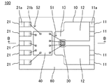
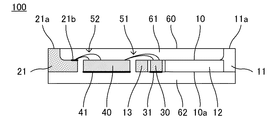
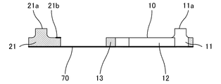
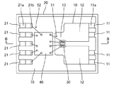
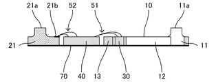
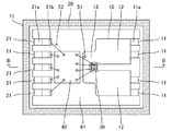
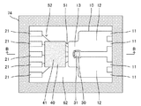
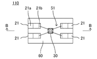
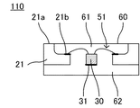
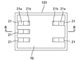
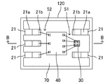
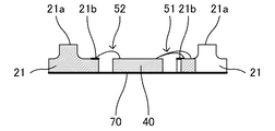
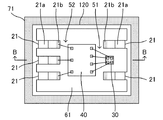
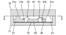
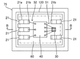
図1A及び図1Bは、本実施形態に係る電流センサ100の構成を示す。ここで、図1Aは、電流センサ100の内部構成を平面視において示し、図1Bは、図1Aにおける基準線BBに関して電流センサ100の断面構成を示す。なお、図1Aにおける上下方向を縦方向、図1A及び図1Bにおける左右方向を横方向、及び図1Bにおける上下方向を高さ方向とする。また、図1A及び図1B並びにこれらに対応するその他の図において、パッケージ60(第1及び第2封止部材61,62)を透過して電流センサ100の内部構成を表している。電流センサ100は、絶縁耐性の高い電流センサを提供することを目的とする電流検出装置の一例であり、導体10、複数のデバイス端子21、磁気センサ30、信号処理IC40、ワイヤ51,52、及びパッケージ60を備える。 1A and 1B show the configuration of the current sensor 100 according to the present embodiment. Here, FIG. 1A shows the internal configuration of the current sensor 100 in a plan view, and FIG. 1B shows a cross-sectional configuration of the current sensor 100 with respect to the reference line BB in FIG. 1A. The vertical direction in FIG. 1A is the vertical direction, the horizontal direction in FIGS. 1A and 1B is the horizontal direction, and the vertical direction in FIG. 1B is the height direction. Further, in FIGS. 1A and 1B and other drawings corresponding thereto, the internal configuration of the current sensor 100 is shown through the package 60 (first and second sealing members 61, 62). The current sensor 100 is an example of a current detection device for the purpose of providing a current sensor having high insulation resistance, and includes a conductor 10, a plurality of device terminals 21, a magnetic sensor 30, a signal processing IC 40, wires 51, 52, and a current sensor 100. The package 60 is provided.

導体10は、電流センサ100により検出される電流(被測定電流と呼ぶ)が電流経路に沿って流れる導電性部材である。導体10は、大きな被測定電流を流すために、例えば銅のような金属等の導電体を用いて0.2mm厚、ただし端子部11は0.4mm厚で、横方向右側に設けられる2組の端子部11のうちの一方の組から後述するパッケージ60の内部を通って他方の組に戻る形状に成形される。導体10は、2組の端子部11、2つの脚部12、及び曲部13を含む。 The conductor 10 is a conductive member in which a current (referred to as a measured current) detected by the current sensor 100 flows along a current path. The conductor 10 has a thickness of 0.2 mm using a conductor such as a metal such as copper in order to pass a large current to be measured, but the terminal portion 11 has a thickness of 0.4 mm and is provided in two sets on the right side in the lateral direction. It is formed into a shape that returns from one set of the terminal portions 11 to the other set through the inside of the package 60 described later. The conductor 10 includes two sets of terminal portions 11, two leg portions 12, and a curved portion 13.

2組の端子部11は、被測定電流を入出力する電流端子であり、横方向右側に縦方向に離間して配設されている。2組の端子部11は、平面視において略矩形状を有し、2組の端子部11に含まれる各2つの端子部11が、それぞれの基端(すなわち、左端)の厚みを絞ってそれぞれ2つの脚部12の右端に一体的に接続する。なお、各組の端子部11は、2つの端子部11に限らず、3以上の端子部11を含んでもよい。 The two sets of terminal portions 11 are current terminals for inputting and outputting the current to be measured, and are arranged vertically separated on the right side in the horizontal direction. The two sets of terminal portions 11 have a substantially rectangular shape in a plan view, and each of the two sets of terminal portions 11 included in the two sets of terminal portions 11 has their respective base ends (that is, the left end) reduced in thickness. It is integrally connected to the right end of the two legs 12. The terminal portion 11 of each set is not limited to the two terminal portions 11, and may include three or more terminal portions 11.

2つの脚部12は、2組の端子部11のうちの一方の組の端子部11に入力された電流を曲部13に送る又は曲部13から他方の組の端子部11に電流を送る部材であり、2組の端子部11の左側に、縦方向に離間して配設されている。2つの脚部12は、平面視において横方向を長手とする矩形状を有し、それぞれ、右端に接続する2組の端子部11をそれぞれ曲部13の2つの端部に一体的に接続する。 The two legs 12 send a current input to the terminal portion 11 of one set of the two sets of terminal portions 11 to the curved portion 13, or send a current from the curved portion 13 to the terminal portion 11 of the other set. It is a member and is arranged vertically spaced apart on the left side of the two sets of terminal portions 11. The two legs 12 have a rectangular shape having a longitudinal direction in the plan view, and two sets of terminal portions 11 connected to the right ends are integrally connected to the two ends of the curved portion 13, respectively. ..

曲部13は、2つの脚部12の一方から流れ込む電流の向きを逆向きに変えて他方の脚部12に送り出す部材であり、2つの脚部12の左側に配設されている。曲部13は、平面視において胴部とこれを間に連ねる2つの端部を有してU字状に成形され、胴部を左側に向けて、2つの端部をそれぞれ2つの脚部12に一体的に接続する。ここで、曲部13の内側に形成される空間の幅は、磁気センサ30の幅より大きい。 The curved portion 13 is a member that changes the direction of the current flowing from one of the two leg portions 12 in the opposite direction and sends the current to the other leg portion 12, and is arranged on the left side of the two leg portions 12. The curved portion 13 is formed in a U shape having a trunk portion and two ends connecting the trunk portion in a plan view, and the trunk portion is directed to the left side, and the two ends are each with two leg portions 12. Connect integrally to. Here, the width of the space formed inside the curved portion 13 is larger than the width of the magnetic sensor 30.

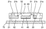
なお、導体10の底面10aを粗面加工してもよい。ここで、粗面加工された底面10aの算術平均粗さ(Ra)は0.01μm以上とする。それにより、導体10を封止するパッケージ60が導体10の底面10aに密着し、界面の形成が抑止される。 The bottom surface 10a of the conductor 10 may be roughened. Here, the arithmetic average roughness (Ra) of the roughened bottom surface 10a is 0.01 μm or more. As a result, the package 60 that seals the conductor 10 comes into close contact with the bottom surface 10a of the conductor 10, and the formation of an interface is suppressed.

なお、導体10の肉厚部(すなわち、端子部11)の上面11aを除いて薄肉部(すなわち、脚部12及び曲部13)の上面に例えば銀を用いてメッキ膜を設けてもよい。 A plating film may be provided on the upper surface of the thin portion (that is, the leg portion 12 and the curved portion 13) except for the upper surface 11a of the thick portion (that is, the terminal portion 11) of the conductor 10.

導体10は、2組の端子部11にそれぞれ含まれる端子部11の上面及び先端面(すなわち、右端面)をパッケージ60の上面及び右側面に面一に露出して、パッケージ60内に封止されている。端子部11の上面11aは、電流センサ100を例えば外部基板上に実装した際に、外部基板上に配設された配線等に接合される。被測定電流は、縦方向の上側(又は下側)の一方の組の端子部11から入力され、上側(又は下側)の脚部12を介して曲部13を流れることでその向きを左向きから右向きに180度を変え、下側(又は上側)の脚部12を介して下側(又は上側)の他方の組の端子部11から出力される。なお、被測定電流が導体10内を流れる経路を電流経路と呼ぶ。 The conductor 10 exposes the upper surface and the tip surface (that is, the right end surface) of the terminal portions 11 included in the two sets of terminal portions 11 flushly with the upper surface and the right end surface of the package 60, and seals the conductor 10 in the package 60. Has been done. The upper surface 11a of the terminal portion 11 is joined to wiring or the like arranged on the external board when the current sensor 100 is mounted on the external board, for example. The measured current is input from one set of terminal portions 11 on the upper side (or lower side) in the vertical direction, and flows through the curved portion 13 via the upper (or lower side) leg portion 12 to turn the direction to the left. It changes 180 degrees to the right from, and is output from the other set of terminal portions 11 on the lower side (or upper side) via the lower (or upper side) leg portion 12. The path through which the measured current flows in the conductor 10 is called a current path.

複数のデバイス端子21は、信号処理IC40から出力される電流量の算出結果を外部デバイスに出力する、また補正パラメータを設定するための信号を外部デバイスから信号処理IC40に入力する信号端子である。複数のデバイス端子21は、一例として5つの端子を含み、横方向左側に縦方向に離間して配設されている。複数のデバイス端子21のそれぞれは、例えば銅のような金属等の導電体を用いて0.2mm厚、ただし左端部は0.4mm厚で、横方向を長手とする矩形状に成形される。 The plurality of device terminals 21 are signal terminals that output the calculation result of the amount of current output from the signal processing IC 40 to the external device and input the signal for setting the correction parameter from the external device to the signal processing IC 40. The plurality of device terminals 21 include five terminals as an example, and are arranged vertically separated on the left side in the horizontal direction. Each of the plurality of device terminals 21 is 0.2 mm thick using a conductor such as a metal such as copper, but the left end portion is 0.4 mm thick and is formed into a rectangular shape having a longitudinal length in the lateral direction.

なお、複数のデバイス端子21の肉厚部(すなわち、左端部)の上面21aを除いて薄肉部の上面に例えば銀を用いてメッキ膜を設けてもよい。 A plating film may be provided on the upper surface of the thin portion except for the upper surface 21a of the thick portion (that is, the left end portion) of the plurality of device terminals 21 using, for example, silver.

複数のデバイス端子21は、左端部の上面21a及び先端面(すなわち、左端面)をパッケージ60の上面及び左側面に面一に露出して、パッケージ60内に封止されている。デバイス端子21の上面21aは、電流センサ100を例えば外部基板上に実装した際に、外部基板上に配設された配線等に接合される。 The plurality of device terminals 21 are sealed in the package 60 by exposing the upper surface 21a and the tip surface (that is, the left end surface) of the left end portion flushly to the upper surface and the left side surface of the package 60. The upper surface 21a of the device terminal 21 is joined to wiring or the like arranged on the external board when the current sensor 100 is mounted on the external board, for example.

磁気センサ30は、導体10に流れる電流により発生する磁場を検出する磁気検出素子の一例である。磁気センサ30として、例えば、InAs、GaAs等から構成される化合物半導体ホール素子、シリコンから構成されるホール素子(或いは増幅回路と一体化されたホールIC)、及び磁気抵抗素子を採用することができる。磁気センサ30は、導体10の曲部13の内側、好ましくは曲部13内における電流経路の曲率中心に配置される。それにより、曲部13に流れる電流により発生する磁場が磁気センサ30に集束し、磁気センサ30により高いSN比で磁場を検出することが可能となる。さらにより高いSN比で地場を検出するには、磁気センサ30の厚さは、導体10の厚さより薄い方が好ましい。 The magnetic sensor 30 is an example of a magnetic detection element that detects a magnetic field generated by a current flowing through a conductor 10. As the magnetic sensor 30, for example, a compound semiconductor Hall element composed of InAs, GaAs, etc., a Hall element composed of silicon (or a Hall IC integrated with an amplification circuit), and a magnetic resistance element can be adopted. .. The magnetic sensor 30 is arranged inside the curved portion 13 of the conductor 10, preferably at the center of curvature of the current path in the curved portion 13. As a result, the magnetic field generated by the current flowing through the curved portion 13 is focused on the magnetic sensor 30, and the magnetic field can be detected by the magnetic sensor 30 at a high SN ratio. In order to detect the local area with an even higher SN ratio, the thickness of the magnetic sensor 30 is preferably thinner than the thickness of the conductor 10.

なお、磁気センサ30の底面に絶縁部材31を設けてもよい。絶縁部材31は、粗面加工されたものでもよく、その算術平均粗さ(Ra)は0.01μm以上とする。絶縁部材31として、例えば、ウエハをダイシングして、ウエハ上に形成された磁気センサ30の回路素子を個片化する際に、ウエハの裏面に貼り付けられるダイアタッチフィルムを採用することができる。絶縁部材31により磁気センサ30の底面が(例えば、後述するウェットブラスト時において)保護され、また絶縁部材31が0.01μm以上の算術平均粗さ(Ra)で粗面加工されていることで、パッケージ60が磁気センサ30の底面に密着してこれを封止することにより界面の形成が抑止される。プラズマ処理等の磁気センサ30の底面に大きなダメージが無い方法であり、保護する必要がない場合は、絶縁部材31は無くてもよい。 An insulating member 31 may be provided on the bottom surface of the magnetic sensor 30. The insulating member 31 may have a roughened surface, and its arithmetic average roughness (Ra) is 0.01 μm or more. As the insulating member 31, for example, a die attach film attached to the back surface of the wafer can be adopted when the wafer is diced to separate the circuit elements of the magnetic sensor 30 formed on the wafer. The bottom surface of the magnetic sensor 30 is protected by the insulating member 31 (for example, during wet blasting described later), and the insulating member 31 is roughened with an arithmetic mean roughness (Ra) of 0.01 μm or more. The formation of the interface is suppressed by the package 60 coming into close contact with the bottom surface of the magnetic sensor 30 and sealing the package 60. If the method is such that the bottom surface of the magnetic sensor 30 is not significantly damaged by plasma processing or the like and does not need to be protected, the insulating member 31 may be omitted.

なお、磁気センサ30の上側、下側、又は両側に磁性体メッキにより形成された磁性体を設け、それらにより磁場を集束して磁気センサ30に入力することとしてもよい。また、磁気センサ30の上面、下面、又は両面を、例えばアルミニウム等の非磁性導体を用いて静電シールドして、パッケージ60外から来る静電ノイズを遮蔽してもよい。 In addition, a magnetic material formed by magnetic material plating may be provided on the upper side, the lower side, or both sides of the magnetic sensor 30, and the magnetic field may be focused by them and input to the magnetic sensor 30. Further, the upper surface, the lower surface, or both surfaces of the magnetic sensor 30 may be electrostatically shielded by using a non-magnetic conductor such as aluminum to shield the electrostatic noise coming from the outside of the package 60.

なお、磁気センサ30に入力する外部磁場等にともなうノイズを除くために、導体10の曲部13の外側に外部磁場を検出するための追加の磁気センサを設けてもよい。斯かる場合、信号処理IC40により磁気センサ30の検出信号と追加の磁気センサの検出信号との差分を算出することで、磁気センサ30の検出信号に含まれる外部磁場等に由来するノイズを相殺することができる。 An additional magnetic sensor for detecting an external magnetic field may be provided outside the curved portion 13 of the conductor 10 in order to remove noise due to an external magnetic field or the like input to the magnetic sensor 30. In such a case, the signal processing IC 40 calculates the difference between the detection signal of the magnetic sensor 30 and the detection signal of the additional magnetic sensor to cancel the noise derived from the external magnetic field or the like included in the detection signal of the magnetic sensor 30. be able to.

磁気センサ30は、ワイヤボンディングによって信号処理IC40に接続され、検出した磁場の強度に応じた電圧を出力信号として信号処理IC40に出力する。 The magnetic sensor 30 is connected to the signal processing IC 40 by wire bonding, and outputs a voltage corresponding to the detected magnetic field strength to the signal processing IC 40 as an output signal.

信号処理IC40は、磁気センサ30が出力する信号を処理して、導体10に流れる電流の量を算出するデバイスである。信号処理IC40は、メモリ、感度補正回路、出力のオフセットを補正するオフセット補正回路、磁気センサ30からの出力信号を増幅する増幅回路、及び温度に応じて出力を補正する温度補正回路等の少なくとも1つを内蔵してもよい。本実施形態では、信号処理IC40は、磁気センサ30と別個のデバイスとしてハイブリッド構成されたものを採用する。信号処理IC40は、導体10の曲部13と複数のデバイス端子21との間に配置される。 The signal processing IC 40 is a device that processes a signal output by the magnetic sensor 30 to calculate the amount of current flowing through the conductor 10. The signal processing IC 40 includes at least one such as a memory, a sensitivity correction circuit, an offset correction circuit that corrects an output offset, an amplifier circuit that amplifies an output signal from the magnetic sensor 30, and a temperature correction circuit that corrects an output according to temperature. It may be built-in. In the present embodiment, the signal processing IC 40 adopts a hybrid configuration as a device separate from the magnetic sensor 30. The signal processing IC 40 is arranged between the curved portion 13 of the conductor 10 and the plurality of device terminals 21.

なお、信号処理IC40の底面に絶縁部材41を設けてもよい。絶縁部材41は、粗面加工されたものでもよく、その算術平均粗さ(Ra)は0.01μm以上とする。絶縁部材41として、例えば、ウエハをダイシングして、ウエハ上に形成された信号処理IC40の回路素子を個片化する際に、ウエハの裏面に貼り付けられるダイアタッチフィルムを採用することができる。絶縁部材41により信号処理IC40の底面が(例えば、後述するウェットブラスト時において)保護され、また絶縁部材41が0.01μm以上の算術平均粗さ(Ra)で粗面加工されていることで、パッケージ60が信号処理IC40の底面に密着してこれを封止することにより界面の形成が抑止される。 An insulating member 41 may be provided on the bottom surface of the signal processing IC 40. The insulating member 41 may have a roughened surface, and its arithmetic average roughness (Ra) is 0.01 μm or more. As the insulating member 41, for example, a die attach film attached to the back surface of the wafer can be adopted when the wafer is diced to separate the circuit elements of the signal processing IC 40 formed on the wafer. The bottom surface of the signal processing IC 40 is protected by the insulating member 41 (for example, during wet blasting described later), and the insulating member 41 is roughened with an arithmetic average roughness (Ra) of 0.01 μm or more. The formation of the interface is suppressed by the package 60 coming into close contact with the bottom surface of the signal processing IC 40 and sealing the package 60.

なお、本実施形態においては、信号処理IC40がリードフレーム等によって支持されていない形態を示しているが、信号処理IC40は例えばリードフレーム上に載置されてもよい。また絶縁部材41は、前述のように無くてもよい。 Although the signal processing IC 40 is not supported by a lead frame or the like in the present embodiment, the signal processing IC 40 may be mounted on the lead frame, for example. Further, the insulating member 41 may be omitted as described above.

信号処理IC40は、ワイヤボンディングによって複数のデバイス端子21に接続され、それらを介して導体10に流れる電流の量の算出結果を出力する、さらにパラメータの設定等を入力する。なお、複数のデバイス端子21のいずれかをグランド端子として使用してもよい。また、信号処理IC40の上面、下面、又は両面を、例えばアルミニウム等の非磁性導体を用いて静電シールドして、パッケージ60外から来る静電ノイズを遮蔽してもよい。 The signal processing IC 40 is connected to a plurality of device terminals 21 by wire bonding, outputs a calculation result of the amount of current flowing through the conductor 10 through them, and further inputs parameter settings and the like. Any one of the plurality of device terminals 21 may be used as the ground terminal. Further, the upper surface, the lower surface, or both surfaces of the signal processing IC 40 may be electrostatically shielded by using a non-magnetic conductor such as aluminum to shield the electrostatic noise coming from the outside of the package 60.

なお、本実施形態に係る電流センサ100では、磁気センサ30と別個のデバイスとしてハイブリッド構成された信号処理IC40を採用したが、これに代えて、磁気センサ30と同一の半導体基板上に形成された信号処理回路を備える信号処理IC、すなわち磁気センサ30とともにモノリシック構成された信号処理ICを採用してもよい。斯かる場合、導体10の曲部13を同一の半導体基板の上方又は下方にクリアランスを設けて配置し、平面視において導体10の曲部13の内側に同一の半導体基板上の磁気センサ30を位置決めし、パッケージ60により同一の半導体基板を導体10から離間するとともに全ての外面を覆って封止する。また、磁気センサ30と信号処理IC40とが同一の回路基板上にマウントされた、ハイブリッド型の信号処理ICを採用しても良い。 In the current sensor 100 according to the present embodiment, the signal processing IC 40 hybridly configured as a device separate from the magnetic sensor 30 is adopted, but instead, it is formed on the same semiconductor substrate as the magnetic sensor 30. A signal processing IC provided with a signal processing circuit, that is, a signal processing IC having a monolithic configuration may be adopted together with the magnetic sensor 30. In such a case, the curved portion 13 of the conductor 10 is arranged with a clearance above or below the same semiconductor substrate, and the magnetic sensor 30 on the same semiconductor substrate is positioned inside the curved portion 13 of the conductor 10 in a plan view. Then, the same semiconductor substrate is separated from the conductor 10 by the package 60, and the entire outer surface is covered and sealed. Further, a hybrid type signal processing IC in which the magnetic sensor 30 and the signal processing IC 40 are mounted on the same circuit board may be adopted.

ワイヤ51,52は、例えば銅や金のような金属等の導電体を用いて成形された線状部材である。ワイヤ51は、磁気センサ30及び信号処理IC40の間に架設される4つのワイヤを含み、これらを介して磁気センサ30を駆動し、その検出信号を信号処理IC40に送る。ワイヤ52は、信号処理IC40及び複数のデバイス端子21の上面21bの間に架設される5つのワイヤを含み、これらを介して信号処理IC40の算出結果を出力する。 The wires 51 and 52 are linear members formed by using a conductor such as a metal such as copper or gold. The wire 51 includes four wires erected between the magnetic sensor 30 and the signal processing IC 40, drives the magnetic sensor 30 through these wires, and sends the detection signal to the signal processing IC 40. The wire 52 includes five wires erected between the signal processing IC 40 and the upper surface 21b of the plurality of device terminals 21, and outputs the calculation result of the signal processing IC 40 via these five wires.

パッケージ60は、複数のデバイス端子21及び導体10の一部を除いて電流センサ100の構成各部を封止して、保護する封止部材の一例である。ここで、パッケージ60は、磁気センサ30及び信号処理IC40のそれぞれを導体10及び複数のデバイス端子21から離間してそれらとともにそれぞれの外面全面を覆って内部に封止し、それにより導体10と複数のデバイス端子21とを絶縁する。磁気センサ30(信号処理IC40と同一の回路基板上にマウントされている場合の信号処理IC及び回路基板など、磁気センサ30に接する部材も含むものとする)は、例えば導体10及びデバイス端子21と接するように配置された基板、フィルム等に接して支持されることなく、全ての外面がパッケージ60により覆われて封止される。ここで、「全ての外面」とは、磁気センサ30を信号処理IC40と接続するためのボンディングワイヤ等の導体の接続部分を除く外面の全てがパッケージ60で覆われていることをいう。また、磁気センサ31の底面に絶縁部材31が備えられている場合には、絶縁部材31の表面を磁気センサ31の外面とする。 The package 60 is an example of a sealing member that seals and protects each component of the current sensor 100 except for a part of the plurality of device terminals 21 and the conductor 10. Here, the package 60 separates each of the magnetic sensor 30 and the signal processing IC 40 from the conductor 10 and the plurality of device terminals 21 and together with them covers the entire outer surface of each and seals the inside thereof. Insulate from the device terminal 21 of. The magnetic sensor 30 (including a member in contact with the magnetic sensor 30 such as a signal processing IC and a circuit board when mounted on the same circuit board as the signal processing IC 40) is in contact with, for example, the conductor 10 and the device terminal 21. All outer surfaces are covered and sealed by the package 60 without being in contact with and supported by the substrate, film, etc. arranged in. Here, "all outer surfaces" means that all the outer surfaces except the connection portion of the conductor such as the bonding wire for connecting the magnetic sensor 30 to the signal processing IC 40 are covered with the package 60. When the insulating member 31 is provided on the bottom surface of the magnetic sensor 31, the surface of the insulating member 31 is used as the outer surface of the magnetic sensor 31.

パッケージ60は、例えば、エポキシなどの絶縁性に優れた樹脂を用いてモールド成形することで、矩形状の上面及び上面の一辺の長さより小さい厚さを有する直方体状に成形される。導体10及び複数のデバイス端子21から離間して磁気センサ30及び信号処理IC40をパッケージ60の内部に埋め込んだことで、すなわちそれら単体で埋め込んだことで、パッケージ60に磁気センサ30及び信号処理IC40のそれぞれとの境から拡がり得る界面が形成されないため、高い耐圧を得ることができる。また、磁気センサ30及び信号処理IC40を支持するリードフレームが不要となることで、電流センサ100の小型化が可能となる。また、導体10を半抜き等による段差加工を施して磁気センサ30を囲む曲部13を磁気センサ30を支持するフレームに対して上げる又は下げる必要がないことで、段差加工による導体10の抵抗の増大を避けることができる。 The package 60 is molded into a rectangular parallelepiped shape having a thickness smaller than the length of one side of the rectangular upper surface and the upper surface by molding using, for example, a resin having excellent insulating properties such as epoxy. By embedding the magnetic sensor 30 and the signal processing IC 40 inside the package 60 apart from the conductor 10 and the plurality of device terminals 21, that is, by embedding them alone, the magnetic sensor 30 and the signal processing IC 40 are embedded in the package 60. Since an interface that can be expanded from the boundary with each is not formed, a high withstand voltage can be obtained. Further, by eliminating the need for a lead frame that supports the magnetic sensor 30 and the signal processing IC 40, the current sensor 100 can be miniaturized. Further, since it is not necessary to raise or lower the curved portion 13 surrounding the magnetic sensor 30 with respect to the frame supporting the magnetic sensor 30 by performing step processing such as half-cutting the conductor 10, the resistance of the conductor 10 due to the step processing is increased. The increase can be avoided.

パッケージ60は、導体10、複数のデバイス端子21、磁気センサ30、及び信号処理IC40の少なくとも上面を含む上面側及び少なくとも底面を含む底面側をそれぞれ封止する第1及び第2封止部材61,62を含む。なお、導体10、複数のデバイス端子21、磁気センサ30、及び信号処理IC40の上面に加えてそれらの側面を含んで上面側としてもよく、斯かる場合、底面側に側面は含まないこととする。また、導体10、複数のデバイス端子21、磁気センサ30、及び信号処理IC40の上面のみを含んで上面側としてもよく、斯かる場合、底面側に側面を含むこととする。また、導体10、複数のデバイス端子21、磁気センサ30、及び信号処理IC40の上面に加えてそれらの側面の一部を含んで上面側としてもよく、斯かる場合、底面側に側面の残りの部分を含むこととする。 The package 60 includes the conductor 10, the plurality of device terminals 21, the magnetic sensor 30, and the first and second sealing members 61 that seal the upper surface side including at least the upper surface and the bottom surface side including at least the bottom surface of the signal processing IC 40, respectively. 62 is included. In addition to the upper surface of the conductor 10, the plurality of device terminals 21, the magnetic sensor 30, and the signal processing IC 40, the upper surface side may be included, and in such a case, the bottom surface side is not included. .. Further, only the upper surface of the conductor 10, the plurality of device terminals 21, the magnetic sensor 30, and the signal processing IC 40 may be included on the upper surface side, and in such a case, the side surface is included on the bottom surface side. Further, in addition to the upper surface of the conductor 10, the plurality of device terminals 21, the magnetic sensor 30, and the signal processing IC 40, a part of the side surface thereof may be included as the upper surface side, and in such a case, the remaining side surface is on the bottom surface side. It shall include the part.

後述するように、導体10、複数のデバイス端子21、磁気センサ30、及び信号処理IC40の底面を支持してそれらの上面側を第1封止部材61により覆い、導体10、磁気センサ30、及び信号処理IC40の上下を返して、第1封止部材61により覆われた上面側を除くそれらの底面側を第2封止部材62により覆うことで、磁気センサ30及び信号処理IC40を導体10及び複数のデバイス端子21から離間するとともにそれらの外面全面を覆ってパッケージ60内に単体で埋め込み、封止することができる。なお、第1及び第2封止部材61,62は、同一材料が好ましいが、それぞれ異なる材料を用いて形成してもよい。また、第1及び第2封止部材61,62の少なくとも一方は、無機物の材料であるフィラーを含む材料によって形成されていても良い。 As will be described later, the conductor 10, the plurality of device terminals 21, the magnetic sensor 30, and the bottom surface of the signal processing IC 40 are supported and the upper surface side thereof is covered with the first sealing member 61, and the conductor 10, the magnetic sensor 30, and the signal processing IC 40 are covered. By turning the signal processing IC 40 upside down and covering the bottom surface side thereof except the upper surface side covered with the first sealing member 61 with the second sealing member 62, the magnetic sensor 30 and the signal processing IC 40 are covered with the conductor 10 and the signal processing IC 40. It can be separated from the plurality of device terminals 21 and can be individually embedded and sealed in the package 60 by covering the entire outer surface thereof. The first and second sealing members 61 and 62 are preferably made of the same material, but may be formed by using different materials. Further, at least one of the first and second sealing members 61 and 62 may be formed of a material containing a filler which is an inorganic material.

本実施形態に係る電流センサ100によれば、パッケージ60により、被測定電流が流れる導体10の曲部13とともに、導体10を流れる電流により発生する磁場を検出する磁気センサ30及び磁気センサ30からの出力信号を処理する信号処理IC40を導体10及び複数のデバイス端子21から離間するとともにそれらの外面全面を覆って封止することで、磁気センサ30及び信号処理IC40を内部に埋め込んだパッケージ60にそれらとの境から拡がり得る界面が形成されないため高い耐圧を得ることができる。 According to the current sensor 100 according to the present embodiment, the package 60 is from the magnetic sensor 30 and the magnetic sensor 30 that detect the magnetic field generated by the current flowing through the conductor 10 together with the curved portion 13 of the conductor 10 through which the measured current flows. By separating the signal processing IC 40 for processing the output signal from the conductor 10 and the plurality of device terminals 21 and covering and sealing the entire outer surface thereof, the magnetic sensor 30 and the signal processing IC 40 are embedded in the package 60. A high withstand voltage can be obtained because an interface that can expand from the boundary with the above is not formed.

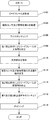
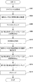
本実施形態に係る電流センサ100の製造方法について説明する。図2に、本実施形態に係る電流センサの製造工程のフローを示す。 A method of manufacturing the current sensor 100 according to the present embodiment will be described. FIG. 2 shows the flow of the manufacturing process of the current sensor according to the present embodiment.

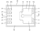
ステップS102では、導体10及び複数のデバイス端子21のパターンを含むリードフレーム20を形成する。図3A及び図3Bに示すように、リードフレーム20は、矩形状の金属フレームであり、その内側に、導体10のパターンをその2組の端子部11をフレームの右枠に接続し、複数のデバイス端子21のパターンをそれらの左端部をフレームの左枠に接続して含む。 In step S102, the lead frame 20 including the pattern of the conductor 10 and the plurality of device terminals 21 is formed. As shown in FIGS. 3A and 3B, the lead frame 20 is a rectangular metal frame, and inside the lead frame 20, a plurality of conductor 10 patterns are connected to the two sets of terminal portions 11 to the right frame of the frame. The patterns of the device terminals 21 are included by connecting their left ends to the left frame of the frame.

なお、本実施形態では、1つのリードフレーム20に1つの電流センサ100を構成する一組の導体10及び複数のデバイス端子21のパターンのみを含むとしたが、これは説明のための一例であり、1つのリードフレーム20に複数の電流センサ100を構成する複数組の導体10及び複数のデバイス端子21が配列されたパターンを含んでもよい。 In this embodiment, one lead frame 20 includes only a set of conductors 10 constituting one current sensor 100 and a pattern of a plurality of device terminals 21, but this is an example for explanation. One lead frame 20 may include a pattern in which a plurality of sets of conductors 10 constituting a plurality of current sensors 100 and a plurality of device terminals 21 are arranged.

まず、例えば一枚の金属板をプレス加工することにより、リードフレーム20の原型を形成する。ここで、金属板は、例えば0.4mm厚を有する。次に、導体10の端子部11に対応するパターン部分の上面11a及び複数のデバイス端子21の左端部に対応するパターン部分の上面21aを除いてリードフレーム20の原型をエッチングすることにより、例えば0.2mm厚で薄肉に成形する。これにより、肉厚の導体10の端子部11及び複数のデバイス端子21の左端部が接続端子として機能する。次に、エッチングにより薄肉化された部分の上面に例えば銀を用いてメッキ膜を設ける。なお、これに代えて、リードフレーム20の上面全体にメッキ膜を設け、後述する第1及び第2封止部材61,62の硬化後に導体10の端子部11の上面11a及び複数のデバイス端子21の左端部の上面21a上のメッキ膜を除去し、例えば錫を用いて新しいメッキ膜を設けてもよい。最後に、リードフレーム20の下面にシート状の支持部材70の外縁を貼り付けて、フレーム内側に底面を設ける。支持部材70として、例えば、粘着層が形成された耐熱性の高いポリイミドテープ、セラミックシート等を採用することができる。 First, for example, a prototype of the lead frame 20 is formed by pressing a single metal plate. Here, the metal plate has a thickness of, for example, 0.4 mm. Next, the prototype of the lead frame 20 is etched, for example, by etching the upper surface 11a of the pattern portion corresponding to the terminal portion 11 of the conductor 10 and the upper surface 21a of the pattern portion corresponding to the left end portion of the plurality of device terminals 21. . Mold to a thin wall with a thickness of 2 mm. As a result, the terminal portion 11 of the thick conductor 10 and the left end portion of the plurality of device terminals 21 function as connection terminals. Next, a plating film is provided on the upper surface of the portion thinned by etching using, for example, silver. Instead of this, a plating film is provided on the entire upper surface of the lead frame 20, and after the first and second sealing members 61 and 62, which will be described later, are cured, the upper surface 11a of the terminal portion 11 of the conductor 10 and the plurality of device terminals 21 are provided. The plating film on the upper surface 21a of the left end portion of the above may be removed, and a new plating film may be provided using, for example, tin. Finally, the outer edge of the sheet-shaped support member 70 is attached to the lower surface of the lead frame 20, and the bottom surface is provided inside the frame. As the support member 70, for example, a polyimide tape having a high heat resistance on which an adhesive layer is formed, a ceramic sheet, or the like can be adopted.

なお、本実施形態に係る電流センサ100の製造方法では、リードフレーム20の原型をエッチングすることにより、接続端子として機能する導体10の端子部11及び複数のデバイス端子21の左端部を形成したが、これに代えて、例えばリードフレーム20を曲げ加工又は半抜き加工することで、導体10の脚部12、曲部13、複数のデバイス端子21の右端部を含むリードフレーム20の内部パターンに対して導体10の端子部11及び複数のデバイス端子21の左端部を含むリードフレーム20の外部パターンを曲げる又は上げることで接続端子を形成してもよい。ここで、曲げ加工する場合、リードフレーム20は例えば0.2mm厚を有するとし、半抜き加工する場合、リードフレーム20は例えば0.3mm厚を有し、0.12〜0.15mmを半抜きすることとする。また、リードレスのパッケージ構造を例にしたが、第1封止部材61又は第2封止部材62の外部でリードフレームが曲げられたリードを有するパッケージ構造としてもよい。 In the method for manufacturing the current sensor 100 according to the present embodiment, the terminal portion 11 of the conductor 10 and the left end portions of the plurality of device terminals 21 that function as connection terminals are formed by etching the prototype of the lead frame 20. Instead of this, for example, by bending or half-cutting the lead frame 20, the internal pattern of the lead frame 20 including the leg portion 12, the curved portion 13, and the right end portion of the plurality of device terminals 21 of the conductor 10 can be obtained. The connection terminal may be formed by bending or raising the external pattern of the lead frame 20 including the terminal portion 11 of the conductor 10 and the left end portion of the plurality of device terminals 21. Here, in the case of bending, the lead frame 20 has a thickness of, for example, 0.2 mm, and in the case of half-cutting, the lead frame 20 has a thickness of, for example, 0.3 mm, and 0.12 to 0.15 mm is half. I will pull it out. Further, although the leadless package structure is taken as an example, the package structure may have a lead in which the lead frame is bent outside the first sealing member 61 or the second sealing member 62.

ステップS104では、リードフレーム20の内側に磁気センサ30及び信号処理IC40をリードフレーム20から離間して設置する。図4A及び図4Bに示すように、リードフレーム20の底面として設けられた支持部材70上で、磁気センサ30を、平面視において導体10の曲部13の内側、好ましくは曲部13内における電流経路の曲率中心に曲部13から離間して配置し、信号処理IC40を、平面視において、導体10の曲部13と複数のデバイス端子21との間にそれぞれから離間して配置する。なお、磁気センサ30及び信号処理IC40は、支持部材70の表面に形成された粘着層により固着される。 In step S104, the magnetic sensor 30 and the signal processing IC 40 are installed inside the lead frame 20 apart from the lead frame 20. As shown in FIGS. 4A and 4B, on the support member 70 provided as the bottom surface of the lead frame 20, the magnetic sensor 30 is placed inside the curved portion 13 of the conductor 10 in a plan view, preferably in the curved portion 13. The signal processing IC 40 is arranged at the center of curvature of the path away from the curved portion 13, and the signal processing IC 40 is arranged separated from each other between the curved portion 13 of the conductor 10 and the plurality of device terminals 21 in a plan view. The magnetic sensor 30 and the signal processing IC 40 are fixed by an adhesive layer formed on the surface of the support member 70.

ステップS106では、図4A及び図4Bに示すように、ワイヤ51により磁気センサ30及び信号処理IC40をワイヤボンディングし、ワイヤ52により信号処理IC40及び複数のデバイス端子21をワイヤボンディングする。 In step S106, as shown in FIGS. 4A and 4B, the magnetic sensor 30 and the signal processing IC 40 are wire-bonded by the wire 51, and the signal processing IC 40 and the plurality of device terminals 21 are wire-bonded by the wire 52.

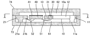
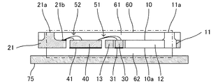
ステップS108では、リードフレーム20、磁気センサ30、及び信号処理IC40の少なくとも上面を含む上面側(本例では上面に加えて側面を含むが、上面のみを含む又は上面に加えて側面の一部を含んでもよい)を第1封止部材61により封止する。図5A及び図5Bに示すように、磁気センサ30及び信号処理IC40が支持部材70上に配置されたリードフレーム20を上面が開いた箱体状の型枠71内に収容し、板状の蓋体72を型枠71上に押しつけてリードフレーム20を含む型枠71の内部空間を閉じ、型枠71の貫通孔(不図示)を介して封止部材を型枠71内に流し込む。ここで、第1封止部材61として、絶縁性材料であるエポキシなどの樹脂を採用することができる。また、第1封止部材61として、フィラーを含む樹脂を採用してもよい。さらに、導体10の端子部11の上面11a及びデバイス端子21の上面21aへの樹脂滲みを防止するために、蓋体72の型枠71側の面を樹脂フィルム(例えば、テフロン(登録商標)フィルム)で覆ってもよい。 In step S108, the upper surface side including at least the upper surface of the lead frame 20, the magnetic sensor 30, and the signal processing IC 40 (in this example, the side surface is included in addition to the upper surface, but only the upper surface is included or a part of the side surface is added to the upper surface. May be included) is sealed by the first sealing member 61. As shown in FIGS. 5A and 5B, the lead frame 20 in which the magnetic sensor 30 and the signal processing IC 40 are arranged on the support member 70 is housed in a box-shaped formwork 71 having an open upper surface, and a plate-shaped lid is provided. The body 72 is pressed onto the mold 71 to close the internal space of the mold 71 including the lead frame 20, and the sealing member is poured into the mold 71 through the through hole (not shown) of the mold 71. Here, as the first sealing member 61, a resin such as epoxy, which is an insulating material, can be adopted. Further, a resin containing a filler may be used as the first sealing member 61. Further, in order to prevent resin bleeding onto the upper surface 11a of the terminal portion 11 of the conductor 10 and the upper surface 21a of the device terminal 21, the surface of the lid 72 on the formwork 71 side is made of a resin film (for example, Teflon (registered trademark) film). ) May be covered.

ステップS110では、リードフレーム20から支持部材70を除去する。第1封止部材61により上面側が封止されたリードフレーム20を型枠71から取り出し、上下を返して、リードフレーム20の下面から支持部材70を剥がす。 In step S110, the support member 70 is removed from the lead frame 20. The lead frame 20 whose upper surface side is sealed by the first sealing member 61 is taken out from the mold 71, turned upside down, and the support member 70 is peeled off from the lower surface of the lead frame 20.

ステップS112では、支持部材70が除去されたリードフレーム20(の導体10及び複数のデバイス端子21の部分)、磁気センサ30、信号処理IC40及び第1封止部材61のそれぞれの底面を粗面加工する。ここで、粗面加工の方法として、例えばウェットブラスト処理又はプラズマ処理を採用することができる。ウェットブラスト処理は、微細粒子を水に含めて表面に吹き付けることにより、微細粒子が衝突して表面の表層が削られるとともに水により異物が流し落とされ、例えばサブミクロンのオーダーで表面を加工する。プラズマ処理は、プラズマを表面に照射することで表面を加工する。リードフレーム20(導体10及び複数のデバイス端子21)、磁気センサ30、及び信号処理IC40のそれぞれの底面の算術平均粗さ(Ra)は0.01μm以上とする。それにより、リードフレーム20の底面側を封止する第2封止部材62が、導体10、磁気センサ30、信号処理IC40及び第1封止部材61のそれぞれの底面に密着する。 In step S112, the bottom surfaces of the lead frame 20 (the conductor 10 and the portions of the plurality of device terminals 21) from which the support member 70 has been removed, the magnetic sensor 30, the signal processing IC 40, and the first sealing member 61 are roughened. do. Here, as a method for rough surface processing, for example, wet blast treatment or plasma treatment can be adopted. In the wet blast treatment, fine particles are included in water and sprayed onto the surface, so that the fine particles collide with each other and the surface layer of the surface is scraped, and at the same time, foreign substances are washed away by water, and the surface is processed, for example, on the order of submicrons. Plasma treatment processes the surface by irradiating the surface with plasma. The arithmetic average roughness (Ra) of the bottom surfaces of the lead frame 20 (conductor 10 and the plurality of device terminals 21), the magnetic sensor 30, and the signal processing IC 40 shall be 0.01 μm or more. As a result, the second sealing member 62 that seals the bottom surface side of the lead frame 20 comes into close contact with the bottom surfaces of the conductor 10, the magnetic sensor 30, the signal processing IC 40, and the first sealing member 61.

なお、リードフレーム20、磁気センサ30、及び信号処理IC40を予め粗面加工することとして、ステップS112を省略してもよい。斯かる場合に、少なくとも導体10及び複数のデバイス端子21の部分が粗化メッキされたリードフレーム20を使用してもよい。 The lead frame 20, the magnetic sensor 30, and the signal processing IC 40 may be roughened in advance, and step S112 may be omitted. In such a case, a lead frame 20 in which at least the conductor 10 and the portions of the plurality of device terminals 21 are coarsely plated may be used.

なお、導体10、磁気センサ30、信号処理IC40及び第1封止部材61の底面が粗面加工されていなくて第2封止部材62がそれらに十分に密着する場合には、ステップS112を省略してもよい。また、リードフレーム20、磁気センサ30、信号処理IC40の底面を予め粗面加工することとしてステップS112を省略してもよい。 If the bottom surfaces of the conductor 10, the magnetic sensor 30, the signal processing IC 40, and the first sealing member 61 are not roughened and the second sealing member 62 is sufficiently in close contact with them, step S112 is omitted. You may. Further, step S112 may be omitted by roughening the bottom surfaces of the lead frame 20, the magnetic sensor 30, and the signal processing IC 40 in advance.

ステップS114では、リードフレーム20、磁気センサ30、及び信号処理IC40の少なくとも底面を含む底面側(本例では底面のみを含むが、ステップS108において上面のみを含む又は上面に加えて側面の一部を含む上面側を第1封止部材61により封止した場合、底面に加えて側面又は側面の残りの部分を含むとする)を第2封止部材62により封止する。ステップS108において成形された第1封止部材61のポストキュアを実施する前に、図6A及び図6Bに示すように、底面が粗面加工されたリードフレーム20を上下を返した状態で上面が開いた箱体状の型枠73内に収容し、底面が開いた箱体状の型枠74を型枠73上に押しつけてリードフレーム20の底面により型枠74の内部空間を閉じ、型枠74の貫通孔(不図示)を介して第2封止部材62を型枠74内に流し込む。ここで、第2封止部材62として、第1封止部材と同じ絶縁性材料であるエポキシなどの樹脂を採用する。また、第2封止部材62として、フィラーを含む樹脂を採用してもよい。それにより、第1封止部材61の樹脂がガラス転移点を超えて柔らかくなっている間に、リードフレーム20に含まれる導体10及び複数のデバイス端子21、磁気センサ30、及び信号処理IC40のそれぞれの底面が第2封止部材62により覆われ、導体10等の底面を覆わない第2封止部材62の境界部分のエポキシ樹脂成分と第1封止部材61の境界部分のエポキシ樹脂成分とが一体化して硬化する。この様な手順で作製することで、後に断面を観察した際に、第2封止部材62中に含まれる無機物の材料であるフィラーで特に20μm以上のサイズのものは、第1封止部材61と第2封止部材62の境界部を跨ぐように存在しないという特徴が観察できる。一体化した第1及び第2封止部材61,62に導体10、複数のデバイス端子21、磁気センサ30、又は信号処理IC40との境から拡がり得る界面が形成されないため高い耐圧を得ることができる。 In step S114, the bottom surface side including at least the bottom surface of the lead frame 20, the magnetic sensor 30, and the signal processing IC 40 (in this example, only the bottom surface is included, but in step S108, only the top surface is included or a part of the side surface is added to the top surface. When the upper surface side including the upper surface is sealed by the first sealing member 61, the side surface or the rest of the side surface is included in addition to the bottom surface) is sealed by the second sealing member 62. Before performing post-cure of the first sealing member 61 formed in step S108, as shown in FIGS. 6A and 6B, the top surface of the lead frame 20 whose bottom surface has been roughened is turned upside down. It is housed in an open box-shaped formwork 73, and the box-shaped formwork 74 having an open bottom is pressed onto the formwork 73, and the internal space of the formwork 74 is closed by the bottom surface of the lead frame 20 to close the formwork. The second sealing member 62 is poured into the mold 74 through the through hole (not shown) of the 74. Here, as the second sealing member 62, a resin such as epoxy, which is the same insulating material as the first sealing member, is adopted. Further, a resin containing a filler may be used as the second sealing member 62. As a result, while the resin of the first sealing member 61 is softened beyond the glass transition point, the conductor 10 and the plurality of device terminals 21, the magnetic sensor 30, and the signal processing IC 40 included in the lead frame 20 are each. The bottom surface of the second sealing member 62 is covered with the second sealing member 62 and does not cover the bottom surface of the conductor 10 or the like. It is integrated and cured. By producing by such a procedure, when the cross section is observed later, the filler which is an inorganic material contained in the second sealing member 62 and has a size of 20 μm or more is particularly the first sealing member 61. And the feature that it does not exist so as to straddle the boundary portion of the second sealing member 62 can be observed. High withstand voltage can be obtained because an interface that can extend from the boundary between the conductor 10, the plurality of device terminals 21, the magnetic sensor 30, or the signal processing IC 40 is not formed on the integrated first and second sealing members 61 and 62. ..

ステップS116では、第1及び第2封止部材61,62のポストキュアを実施する。それにより、第1及び第2封止部材61,62がそれらの境界部分を一体化してポストキュアすることで未硬化の割合が低減し、パッケージ60をなし、そのパッケージ60により磁気センサ30及び信号処理IC40がリードフレーム20に含まれる導体10及び複数のデバイス端子21から離間して内部に、ただしリードフレーム20のフレーム並びにこれと導体10の端子部11及び複数のデバイス端子21とを連結する部分を残して、封止される。 In step S116, post-cure of the first and second sealing members 61 and 62 is performed. As a result, the first and second sealing members 61 and 62 integrally post-cure their boundary portions, thereby reducing the uncured ratio, forming a package 60, and the package 60 forms a magnetic sensor 30 and a signal. A portion where the processing IC 40 is separated from the conductor 10 and the plurality of device terminals 21 included in the lead frame 20 and internally, but the frame of the lead frame 20 and the terminal portion 11 of the conductor 10 and the plurality of device terminals 21 are connected to each other. Is sealed, leaving behind.

なお、上述のように第1及び第2封止部材61,62をそれら両方の形成後に同時にポストキュアすることは、第1及び第2封止部材61,62の境界部分が一体化してそれらの間に界面が形成されないことで有効であるが、界面が形成されない又は形成されても無視できる程度であれば、第1封止部材61のポストキュアし、その後に第2封止部材62をポストキュアしてもよい。 In addition, as described above, when the first and second sealing members 61 and 62 are post-cured at the same time after the formation of both of them, the boundary portions of the first and second sealing members 61 and 62 are integrated and they are integrated. It is effective that no interface is formed between them, but if the interface is not formed or is negligible even if it is formed, the first sealing member 61 is post-cured, and then the second sealing member 62 is posted. You may cure.

ステップS118では、パッケージ60をダイシングする。図7A及び図7Bに示すように、パッケージ60の上下を返してダイシングテープ75上に貼り付け、パッケージ60から露出するパターン、すなわちリードフレーム20のフレームと導体10の端子部11及び複数のデバイス端子21とを連結する部分を第1封止部材61の外縁とともに切断する。それにより、導体10の端子部11の上面11a及び複数のデバイス端子21の上面21aがパッケージ60の上面から面一に露出して接続端子をなすことで、電流センサ100が完成する。 In step S118, the package 60 is diced. As shown in FIGS. 7A and 7B, the package 60 is turned upside down and attached onto the dicing tape 75, and the pattern exposed from the package 60, that is, the frame of the lead frame 20, the terminal portion 11 of the conductor 10, and the plurality of device terminals. The portion connecting with 21 is cut together with the outer edge of the first sealing member 61. As a result, the upper surface 11a of the terminal portion 11 of the conductor 10 and the upper surface 21a of the plurality of device terminals 21 are exposed flush with each other from the upper surface of the package 60 to form a connection terminal, thereby completing the current sensor 100.

本実施形態に係る電流センサ100の製造方法によれば、支持部材70上に導体10及び複数のデバイス端子21を含むリードフレーム20、磁気センサ30、及び信号処理IC40を互いに離間して配置し、それぞれの少なくとも上面を含む上面側を第1封止部材61により封止し、支持部材70を除去した後、それぞれの底面を含む上面側以外の底面側を第2封止部材62により封止することで、第1及び第2封止部材61,62が一体化してなるパッケージ60により、被測定電流が流れる導体10の曲部13、導体10に流れる電流により発生する磁場を検出する磁気センサ30、磁気センサ30からの出力信号を処理する信号処理IC40が互いに離間するとともにそれぞれの外面全面を覆って封止され、磁気センサ30及び信号処理IC40を内部に埋め込んだパッケージ60にそれらとの境から拡がり得る界面が形成されないため高い耐圧を得ることができる。 According to the method for manufacturing the current sensor 100 according to the present embodiment, the lead frame 20 including the conductor 10 and the plurality of device terminals 21, the magnetic sensor 30, and the signal processing IC 40 are arranged on the support member 70 so as to be separated from each other. The upper surface side including at least the upper surface of each is sealed by the first sealing member 61, the support member 70 is removed, and then the bottom surface side other than the upper surface side including each bottom surface is sealed by the second sealing member 62. As a result, the magnetic sensor 30 that detects the magnetic field generated by the current flowing through the conductor 10 and the curved portion 13 of the conductor 10 through which the measured current flows by the package 60 in which the first and second sealing members 61 and 62 are integrated. The signal processing ICs 40 that process the output signal from the magnetic sensor 30 are separated from each other and are sealed so as to cover the entire outer surface of the respective outer surfaces. Since a expandable interface is not formed, a high withstand voltage can be obtained.

なお、本実施形態に係る電流センサ100では、パッケージ60は、導体10の端子部11及び複数のデバイス端子21にリードを有さないリードレスパッケージとして成形することとしたが、これに代えて、リードを有するパッケージとして成形してもよい。 In the current sensor 100 according to the present embodiment, the package 60 is molded as a leadless package having no leads in the terminal portion 11 of the conductor 10 and the plurality of device terminals 21, but instead of this, the package 60 is molded. It may be molded as a package with leads.

なお、本実施形態に係る電流センサ100において、導体10に流れる電流は、直流であっても交流であってもよい。また、直流の場合において、通電する電流の向きを任意に定めてよい。 In the current sensor 100 according to the present embodiment, the current flowing through the conductor 10 may be direct current or alternating current. Further, in the case of direct current, the direction of the energized current may be arbitrarily determined.

なお、本実施形態に係る電流センサ100の製造方法では、型枠71〜74を用いた樹脂モールド成形によりパッケージ60を形成したが、これに代えて3Dプリンタを用いてパッケージを形成してもよい。 In the method for manufacturing the current sensor 100 according to the present embodiment, the package 60 is formed by resin molding using the molds 71 to 74, but the package may be formed by using a 3D printer instead. ..

なお、本実施形態に係る電流センサ100は、導体10に電流を流さないで、外部磁場を検出してその強度を測定する磁気検出装置として使用してもよい。斯かる場合、後述する変形例のようにパッケージ60内に導体10を設けなくてもよい。 The current sensor 100 according to the present embodiment may be used as a magnetic detection device that detects an external magnetic field and measures its strength without passing a current through the conductor 10. In such a case, it is not necessary to provide the conductor 10 in the package 60 as in the modification described later.

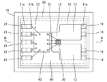
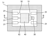
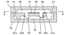
図8A及び図8Bは、変形例に係るホールセンサ110の構成を示す。ここで、図8Aは、ホールセンサ110の内部構成を平面視において示し、図8Bは、図8Aにおける基準線BBに関してホールセンサ110の断面構成を示す。ホールセンサ110は、外部磁場を検出してその強度を測定する磁気検出装置の一例であり、磁気センサ30、複数のデバイス端子21、ワイヤ51、及びパッケージ60を備える。これらの構成各部は、先述の電流センサ100が備えるそれらと同様に構成されてよく、そのため同じ符号を用いて図面中に示すとともに詳細説明を省略することとする。 8A and 8B show the configuration of the Hall sensor 110 according to the modified example. Here, FIG. 8A shows the internal configuration of the Hall sensor 110 in a plan view, and FIG. 8B shows the cross-sectional configuration of the Hall sensor 110 with respect to the reference line BB in FIG. 8A. The Hall sensor 110 is an example of a magnetic detection device that detects an external magnetic field and measures its strength, and includes a magnetic sensor 30, a plurality of device terminals 21, wires 51, and a package 60. Each of these components may be configured in the same manner as those provided in the above-mentioned current sensor 100, and therefore, the same reference numerals will be used and the details will be omitted.

磁気センサ30は、ホールセンサ110に入る磁場(すなわち、外部磁場)を検出する磁気検出素子の一例である。磁気センサ30は、ホールセンサ110の中央に配置される。磁気センサ30は、ワイヤボンディングによって複数のデバイス端子21に接続され、検出した磁場の強度に応じた電圧を出力信号として、例えば複数のデバイス端子21を介してホールセンサ110に接続される信号処理ICに出力する。 The magnetic sensor 30 is an example of a magnetic detection element that detects a magnetic field (that is, an external magnetic field) entering the Hall sensor 110. The magnetic sensor 30 is arranged in the center of the hall sensor 110. The magnetic sensor 30 is connected to a plurality of device terminals 21 by wire bonding, and uses a voltage corresponding to the detected magnetic field strength as an output signal, for example, a signal processing IC connected to the hall sensor 110 via the plurality of device terminals 21. Output to.

複数のデバイス端子21は、磁気センサ30の出力信号を外部デバイスに出力する。複数のデバイス端子21は、一例として4つの端子を含み、磁気センサ30に対して横方向の両側に各2つの端子が縦方向に離間して配設されている。 The plurality of device terminals 21 output the output signal of the magnetic sensor 30 to an external device. The plurality of device terminals 21 include four terminals as an example, and two terminals are arranged on both sides in the horizontal direction with respect to the magnetic sensor 30 so as to be vertically separated from each other.

ワイヤ51は、磁気センサ30及び複数のデバイス端子21の上面21bの間に架設される4つのワイヤを含み、これらを介して磁気センサ30の検出信号を出力する。 The wire 51 includes four wires erected between the magnetic sensor 30 and the upper surfaces 21b of the plurality of device terminals 21, and outputs a detection signal of the magnetic sensor 30 via these four wires.

パッケージ60は、複数のデバイス端子21の一部を除いてホールセンサ110の構成各部を封止して保護する。パッケージ60は、磁気センサ30を複数のデバイス端子21から離間してそれらとともにその外面全面を覆って内部に封止し、それにより複数のデバイス端子21のそれぞれから絶縁する。つまり、磁気センサ30は、例えばデバイス端子21と接するように配置された基板、フィルム等に接して支持されることなく、外面全面がパッケージ60により覆われて封止される。パッケージ60により、その内部に磁気センサ30を複数のデバイス端子21から離間して埋め込んだことで、すなわちそれら単体で埋め込んだことで、パッケージ60に磁気センサ30の境から拡がり得る界面が形成されないため、高い耐圧を得ることができる。また、磁気センサ30を支持するリードフレームが不要となることで、ホールセンサ110の小型化が可能となる。 The package 60 seals and protects each component of the Hall sensor 110 except for a part of the plurality of device terminals 21. The package 60 separates the magnetic sensor 30 from the plurality of device terminals 21 and together with them covers the entire outer surface thereof and seals the inside thereof, thereby insulating from each of the plurality of device terminals 21. That is, the magnetic sensor 30 is sealed by covering the entire outer surface with the package 60 without being supported by contact with, for example, a substrate, a film, or the like arranged so as to be in contact with the device terminal 21. By embedding the magnetic sensor 30 in the package 60 apart from the plurality of device terminals 21, that is, by embedding them alone, the package 60 does not form an interface that can extend from the boundary of the magnetic sensor 30. , High withstand voltage can be obtained. Further, since the lead frame that supports the magnetic sensor 30 is not required, the Hall sensor 110 can be miniaturized.

パッケージ60は、複数のデバイス端子21及び磁気センサ30の少なくとも上面を含む上面側及び少なくとも底面を含む底面側をそれぞれ封止する第1及び第2封止部材61,62を含む。先述の電流センサ100と同様に、複数のデバイス端子21及び磁気センサ30の底面を支持してそれらの上面側を第1封止部材61により覆い、磁気センサ30の上下を返してそれらの底面側を第2封止部材62により覆うことで、磁気センサ30を複数のデバイス端子21から離間するとともにそれらの外面全面を覆ってパッケージ60内に単体で埋め込み、封止することができる。なお、第1及び第2封止部材61,62は、同一材料が好ましいが、それぞれ異なる材料を用いて形成してもよい。 The package 60 includes first and second sealing members 61 and 62 that seal the upper surface side including at least the upper surface side of the plurality of device terminals 21 and the magnetic sensor 30 and the bottom surface side including at least the bottom surface, respectively. Similar to the current sensor 100 described above, the bottom surfaces of the plurality of device terminals 21 and the magnetic sensor 30 are supported, the upper surface side thereof is covered with the first sealing member 61, and the magnetic sensor 30 is turned upside down to the bottom surface side thereof. By covering the magnetic sensor 30 with the second sealing member 62, the magnetic sensor 30 can be separated from the plurality of device terminals 21 and the entire outer surface thereof can be covered and embedded in the package 60 by itself and sealed. The first and second sealing members 61 and 62 are preferably made of the same material, but may be formed by using different materials.

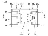
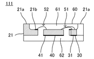
図9A及び図9Bは、変形例に係るホールIC111の構成を示す。ここで、図9Aは、ホールIC111の内部構成を平面視において示し、図9Bは、図9Aにおける基準線BBに関してホールIC111の断面構成を示す。ホールIC111は、外部磁場を検出してその強度を測定する磁気検出装置の一例であり、複数のデバイス端子21、磁気センサ30、信号処理IC40、ワイヤ51,52、及びパッケージ60を備える。これらの構成各部は、先述の電流センサ100が備えるそれらと同様に構成されてよく、そのため同じ符号を用いて図面中に示すとともに詳細説明を省略することとする。 9A and 9B show the configuration of the hall IC 111 according to the modified example. Here, FIG. 9A shows the internal configuration of the Hall IC 111 in a plan view, and FIG. 9B shows the cross-sectional configuration of the Hall IC 111 with respect to the reference line BB in FIG. 9A. The Hall IC 111 is an example of a magnetic detection device that detects an external magnetic field and measures its strength, and includes a plurality of device terminals 21, a magnetic sensor 30, a signal processing IC 40, wires 51, 52, and a package 60. Each of these components may be configured in the same manner as those provided in the above-mentioned current sensor 100, and therefore, the same reference numerals will be used and the details will be omitted.

磁気センサ30は、ホールIC111に入る磁場(すなわち、外部磁場)を検出する磁気検出素子の一例である。磁気センサ30は、ホールIC111の中央右側に配置される。磁気センサ30は、ワイヤボンディングによって信号処理IC40に接続され、検出した磁場の強度に応じた電圧を出力信号として信号処理IC40に出力する。 The magnetic sensor 30 is an example of a magnetic detection element that detects a magnetic field (that is, an external magnetic field) entering the Hall IC 111. The magnetic sensor 30 is arranged on the right side of the center of the hall IC 111. The magnetic sensor 30 is connected to the signal processing IC 40 by wire bonding, and outputs a voltage corresponding to the detected magnetic field strength to the signal processing IC 40 as an output signal.

信号処理IC40は、磁気センサ30が出力する信号を処理して、ホールIC111に入る磁場の強度を算出する。変形例では、信号処理IC40は、磁気センサ30と別個のデバイスとしてハイブリッド構成されたものを採用する。信号処理IC40は、ホールIC111の中央に磁気センサ30と隣接して配置される。信号処理IC40は、ワイヤボンディングによって複数のデバイス端子21に接続され、それらを介して磁場の強度の算出結果を出力する、さらにパラメータの設定等を入力する。なお、複数のデバイス端子21のいずれかをグランド端子として使用してもよい。 The signal processing IC 40 processes the signal output by the magnetic sensor 30 to calculate the strength of the magnetic field entering the Hall IC 111. In the modified example, the signal processing IC 40 adopts a hybrid configuration as a device separate from the magnetic sensor 30. The signal processing IC 40 is arranged adjacent to the magnetic sensor 30 in the center of the hall IC 111. The signal processing IC 40 is connected to a plurality of device terminals 21 by wire bonding, outputs the calculation result of the magnetic field strength through them, and further inputs parameter settings and the like. Any one of the plurality of device terminals 21 may be used as the ground terminal.

なお、変形例に係るホールIC111では、磁気センサ30と別個のデバイスとしてハイブリッド構成された信号処理IC40を採用したが、これに代えて、磁気センサ30と同一の半導体基板上に形成された信号処理回路を備える信号処理IC、すなわち磁気センサ30とともにモノリシック構成された信号処理ICを採用してもよい。また、磁気センサ30と信号処理IC40とが同一の回路基板上にマウントされた、ハイブリッド型の信号処理ICを採用しても良い。 In the Hall IC 111 according to the modified example, the signal processing IC 40 hybridly configured as a device separate from the magnetic sensor 30 is adopted, but instead of this, the signal processing formed on the same semiconductor substrate as the magnetic sensor 30 is adopted. A signal processing IC provided with a circuit, that is, a signal processing IC having a monolithic configuration may be adopted together with the magnetic sensor 30. Further, a hybrid type signal processing IC in which the magnetic sensor 30 and the signal processing IC 40 are mounted on the same circuit board may be adopted.

複数のデバイス端子21は、信号処理IC40から出力される磁場の強度の算出結果を外部デバイスに出力する、また補正パラメータを設定するための信号を外部デバイスから信号処理IC40に入力する。複数のデバイス端子21は、一例として5つの端子を含み、横方向左側に3つの端子が縦方向に離間して、横方向右側に2つの端子が磁気センサ30を間に挟んで縦方向に離間して、それぞれ配設されている。 The plurality of device terminals 21 output the calculation result of the magnetic field strength output from the signal processing IC 40 to the external device, and input the signal for setting the correction parameter from the external device to the signal processing IC 40. The plurality of device terminals 21 include five terminals as an example, three terminals are vertically separated on the left side in the horizontal direction, and two terminals are vertically separated on the right side in the horizontal direction with the magnetic sensor 30 in between. And each is arranged.

ワイヤ51は、磁気センサ30及び信号処理IC40の間に架設される4つのワイヤを含み、これらを介して磁気センサ30を駆動し、その検出信号を信号処理IC40に送る。ワイヤ52は、信号処理IC40及び複数のデバイス端子21の上面21bの間に架設される3つのワイヤを含み、これらを介して信号処理IC40の算出結果を出力する。 The wire 51 includes four wires erected between the magnetic sensor 30 and the signal processing IC 40, drives the magnetic sensor 30 through these wires, and sends the detection signal to the signal processing IC 40. The wire 52 includes three wires erected between the signal processing IC 40 and the upper surface 21b of the plurality of device terminals 21, and outputs the calculation result of the signal processing IC 40 via these three wires.

パッケージ60は、複数のデバイス端子21の一部を除いてホールIC111の構成各部を封止して保護する。パッケージ60は、磁気センサ30及び信号処理IC40のそれぞれを複数のデバイス端子21から離間してそれらとともにそれぞれの外面全面を覆って内部に封止し、それにより複数のデバイス端子21のそれぞれから絶縁する。つまり、磁気センサ30(信号処理IC40と同一の回路基板上にマウントされている場合の信号処理IC及び回路基板など、磁気センサ30に接する部材も含むものとする)は、例えばデバイス端子21と接するように配置された基板、フィルム等に接して支持されることなく、外面全面がパッケージ60により覆われて封止される。パッケージ60により、その内部に磁気センサ30を複数のデバイス端子21から離間して埋め込んだことで、すなわちそれら単体で埋め込んだことで、パッケージ60に磁気センサ30の境から拡がり得る界面が形成されないため、高い耐圧を得ることができる。また、磁気センサ30を支持するリードフレームが不要となることで、ホールIC111の小型化が可能となる。 The package 60 seals and protects each component of the Hall IC 111 except for a part of the plurality of device terminals 21. The package 60 separates each of the magnetic sensor 30 and the signal processing IC 40 from the plurality of device terminals 21 and together with them covers the entire outer surface of each and seals the inside thereof, thereby insulating from each of the plurality of device terminals 21. .. That is, the magnetic sensor 30 (including a member in contact with the magnetic sensor 30 such as a signal processing IC and a circuit board mounted on the same circuit board as the signal processing IC 40) is in contact with, for example, the device terminal 21. The entire outer surface is covered with the package 60 and sealed without being in contact with and supported by the arranged substrate, film, or the like. By embedding the magnetic sensor 30 in the package 60 apart from the plurality of device terminals 21, that is, by embedding them alone, the package 60 does not form an interface that can extend from the boundary of the magnetic sensor 30. , High withstand voltage can be obtained. Further, by eliminating the need for a lead frame that supports the magnetic sensor 30, the hall IC 111 can be miniaturized.

パッケージ60は、複数のデバイス端子21、磁気センサ30、及び信号処理IC40の少なくとも上面を含む上面側及び少なくとも底面を含む底面側をそれぞれ封止する第1及び第2封止部材61,62を含む。複数のデバイス端子21、磁気センサ30、及び信号処理IC40の底面を支持してそれらの上面側を第1封止部材61により覆い、磁気センサ30、及び信号処理IC40の上下を返してそれらの底面側を第2封止部材62により覆うことで、磁気センサ30及び信号処理IC40を複数のデバイス端子21から離間するとともにそれらの外面全面を覆ってパッケージ60内に単体で埋め込み、封止することができる。なお、第1及び第2封止部材61,62は、同一材料が好ましいが、それぞれ異なる材料を用いて形成してもよい。 The package 60 includes a plurality of device terminals 21, a magnetic sensor 30, and first and second sealing members 61 and 62 that seal the upper surface side including at least the upper surface side and the bottom surface side including at least the bottom surface side of the signal processing IC 40, respectively. .. The bottom surfaces of the plurality of device terminals 21, the magnetic sensor 30, and the signal processing IC 40 are supported, the upper surface side thereof is covered with the first sealing member 61, and the bottom surfaces of the magnetic sensor 30 and the signal processing IC 40 are turned upside down. By covering the side with the second sealing member 62, the magnetic sensor 30 and the signal processing IC 40 can be separated from the plurality of device terminals 21 and the entire outer surface thereof can be covered and embedded and sealed in the package 60 by itself. can. The first and second sealing members 61 and 62 are preferably made of the same material, but may be formed by using different materials.

変形例に係るホールIC111の製造方法について説明する。図10に、変形例に係るホールIC111の製造工程のフローを示す。 A method of manufacturing the Hall IC 111 according to a modified example will be described. FIG. 10 shows the flow of the manufacturing process of the Hall IC 111 according to the modified example.

ステップS202では、複数のデバイス端子21のパターンを含むリードフレーム120を形成する。図11A及び図11Bに示すように、リードフレーム120は、矩形状の金属フレームであり、その内側に、複数のデバイス端子21のうちの3つのパターンをそれらの左端部をフレームの左枠に接続し、2つのパターンをそれらの右端部をフレームの右枠に接続して含み、シート状の支持部材70をその外縁をリードフレーム120の下面に貼り付けてその底面として含む。リードフレーム120の製造方法は、先述のリードフレーム20と同様である。 In step S202, a lead frame 120 including a pattern of a plurality of device terminals 21 is formed. As shown in FIGS. 11A and 11B, the lead frame 120 is a rectangular metal frame, and inside the lead frame 120, three patterns of a plurality of device terminals 21 are connected to their left ends to the left frame of the frame. The two patterns are included by connecting their right ends to the right frame of the frame, and the sheet-like support member 70 is included as its bottom surface with its outer edge attached to the lower surface of the lead frame 120. The manufacturing method of the lead frame 120 is the same as that of the lead frame 20 described above.

ステップS204では、リードフレーム120の内側に磁気センサ30及び信号処理IC40をリードフレーム120から離間して設置する。図12A及び図12Bに示すように、リードフレーム120の底面として設けられた支持部材70上で、磁気センサ30を平面視においてリードフレーム120の中央右側に、信号処理IC40を平面視においてリードフレーム120の中央に、複数のデバイス端子21から離間して配置する。なお、磁気センサ30及び信号処理IC40は、支持部材70の表面に形成された粘着層により固着される。 In step S204, the magnetic sensor 30 and the signal processing IC 40 are installed inside the lead frame 120 apart from the lead frame 120. As shown in FIGS. 12A and 12B, on the support member 70 provided as the bottom surface of the lead frame 120, the magnetic sensor 30 is placed on the right side of the center of the lead frame 120 in a plan view, and the signal processing IC 40 is placed in the lead frame 120 in a plan view. It is arranged in the center of the device so as to be separated from the plurality of device terminals 21. The magnetic sensor 30 and the signal processing IC 40 are fixed by an adhesive layer formed on the surface of the support member 70.

ステップS206では、図12A及び図12Bに示すように、ワイヤ51により磁気センサ30及び信号処理IC40をワイヤボンディングし、ワイヤ52により信号処理IC40及び複数のデバイス端子21をワイヤボンディングする。 In step S206, as shown in FIGS. 12A and 12B, the magnetic sensor 30 and the signal processing IC 40 are wire-bonded by the wire 51, and the signal processing IC 40 and the plurality of device terminals 21 are wire-bonded by the wire 52.

ステップS208では、リードフレーム120、磁気センサ30、及び信号処理IC40の少なくとも上面を含む上面側(本例では上面に加えて側面を含むが、上面のみを含む又は上面に加えて側面の一部を含んでもよい)を第1封止部材61により封止する。図13A及び図13Bに示すように、磁気センサ30及び信号処理IC40が支持部材70上に配置されたリードフレーム120を上面が開いた箱体状の型枠71内に収容し、板状の蓋体72を型枠71上に押しつけてリードフレーム120を含む型枠71の内部空間を閉じ、型枠71の貫通孔(不図示)を介して封止部材を型枠71内に流し込む。ここで、第1封止部材61として、エポキシなどの樹脂を採用することができる。また、第1封止部材61として、フィラーを含む樹脂を採用してもよい。さらに、デバイス端子21の上面21aへの樹脂滲みを防止するために、蓋体72の型枠71側の面を樹脂フィルム(例えば、テフロン(登録商標)フィルム)で覆ってもよい。 In step S208, the upper surface side including at least the upper surface of the lead frame 120, the magnetic sensor 30, and the signal processing IC 40 (in this example, the side surface is included in addition to the upper surface, but only the upper surface is included or a part of the side surface is added to the upper surface. May be included) is sealed by the first sealing member 61. As shown in FIGS. 13A and 13B, the lead frame 120 in which the magnetic sensor 30 and the signal processing IC 40 are arranged on the support member 70 is housed in a box-shaped formwork 71 having an open upper surface, and a plate-shaped lid is provided. The body 72 is pressed onto the mold 71 to close the internal space of the mold 71 including the lead frame 120, and the sealing member is poured into the mold 71 through the through hole (not shown) of the mold 71. Here, a resin such as epoxy can be adopted as the first sealing member 61. Further, a resin containing a filler may be used as the first sealing member 61. Further, in order to prevent resin bleeding onto the upper surface 21a of the device terminal 21, the surface of the lid 72 on the mold 71 side may be covered with a resin film (for example, a Teflon (registered trademark) film).

ステップS210では、リードフレーム120から支持部材70を除去する。第1封止部材61により上面側が封止されたリードフレーム120を型枠71から取り出し、上下を返して、リードフレーム120の下面から支持部材70を剥がす。 In step S210, the support member 70 is removed from the lead frame 120. The lead frame 120 whose upper surface side is sealed by the first sealing member 61 is taken out from the mold 71, turned upside down, and the support member 70 is peeled off from the lower surface of the lead frame 120.

ステップS212では、支持部材70が除去されたリードフレーム120(の複数のデバイス端子21の部分)、磁気センサ30、信号処理IC40及び第1封止部材61のそれぞれの底面を粗面加工する。ここで、粗面加工の方法として、例えばウェットブラスト処理又はプラズマ処理を採用することができる。 In step S212, the bottom surfaces of the lead frame 120 (the portion of the plurality of device terminals 21) from which the support member 70 has been removed, the magnetic sensor 30, the signal processing IC 40, and the first sealing member 61 are roughened. Here, as a method for rough surface processing, for example, wet blast treatment or plasma treatment can be adopted.

ステップS214では、リードフレーム120、磁気センサ30、及び信号処理IC40の少なくとも底面を含む底面側(本例では底面のみを含むが、ステップS208において上面のみを含む又は上面に加えて側面の一部を含む上面側を第1封止部材61により封止した場合、底面に加えて側面又は側面の残りの部分を含むとする)を第2封止部材62により封止する。ステップS208において成形された第1封止部材61のポストキュアを実施する前に、図14A及び図14Bに示すように、底面が粗面加工されたリードフレーム120を上下を返した状態で上面が開いた箱体状の型枠73内に収容し、底面が開いた箱体状の型枠74を型枠73上に押しつけてリードフレーム120の底面により型枠74の内部空間を閉じ、型枠74の貫通孔(不図示)を介して第2封止部材62を型枠74内に流し込む。 In step S214, the bottom surface side including at least the bottom surface of the lead frame 120, the magnetic sensor 30, and the signal processing IC 40 (in this example, only the bottom surface is included, but in step S208, only the top surface is included or a part of the side surface is added to the top surface. When the upper surface side including the upper surface is sealed by the first sealing member 61, the side surface or the rest of the side surface is included in addition to the bottom surface) is sealed by the second sealing member 62. Before performing post-cure of the first sealing member 61 formed in step S208, as shown in FIGS. 14A and 14B, the top surface of the lead frame 120 whose bottom surface has been roughened is turned upside down. It is housed in an open box-shaped formwork 73, and the box-shaped formwork 74 with an open bottom is pressed onto the formwork 73, and the internal space of the formwork 74 is closed by the bottom surface of the lead frame 120, and the formwork is closed. The second sealing member 62 is poured into the mold 74 through the through hole (not shown) of the 74.

ステップS216では、第1及び第2封止部材61,62のポストキュアを実施する。それにより、第1及び第2封止部材61,62がそれらの境界部分を一体化してポストキュアすることで未硬化の割合が低減し、パッケージ60をなし、そのパッケージ60により磁気センサ30及び信号処理IC40がリードフレーム20に含まれる複数のデバイス端子21から離間して内部に、ただしリードフレーム120のフレーム並びにこれと複数のデバイス端子21とを連結する部分を残して、封止される。 In step S216, post-cure of the first and second sealing members 61 and 62 is performed. As a result, the first and second sealing members 61 and 62 integrally post-cure their boundary portions, thereby reducing the uncured ratio, forming a package 60, and the package 60 forms a magnetic sensor 30 and a signal. The processing IC 40 is sealed inside, away from the plurality of device terminals 21 included in the lead frame 20, except for the frame of the lead frame 120 and the portion connecting the frame and the plurality of device terminals 21.

ステップS218では、パッケージ60をダイシングする。図15A及び図15Bに示すように、パッケージ60の上下を返してダイシングテープ75上に貼り付け、パッケージ60から露出するパターン、すなわちリードフレーム120のフレームと複数のデバイス端子21とを連結する部分を第1封止部材61の外縁とともに切断する。それにより、複数のデバイス端子21の上面21aがパッケージ60の上面から面一に露出して接続端子をなすことで、ホールIC111が完成する。 In step S218, the package 60 is diced. As shown in FIGS. 15A and 15B, the package 60 is turned upside down and attached onto the dicing tape 75, and the pattern exposed from the package 60, that is, the portion connecting the frame of the lead frame 120 and the plurality of device terminals 21 is formed. It is cut together with the outer edge of the first sealing member 61. As a result, the upper surfaces 21a of the plurality of device terminals 21 are exposed flush with each other from the upper surface of the package 60 to form connection terminals, thereby completing the hall IC 111.

変形例に係るホールIC111の製造方法によれば、支持部材70上に複数のデバイス端子21を含むリードフレーム120、磁気センサ30、及び信号処理IC40を互いに離間して配置し、それぞれの少なくとも上面を含む上面側を第1封止部材61により封止し、支持部材70を除去した後、それぞれの底面を含む上面側以外の底面側を第2封止部材62により封止することで、第1及び第2封止部材61,62が一体化してなるパッケージ60により、磁気センサ30、磁気センサ30からの出力信号を処理する信号処理IC40が互いに離間するとともにそれぞれの外面全面を覆って封止され、磁気センサ30及び信号処理IC40を内部に埋め込んだパッケージ60にそれらとの境から拡がり得る界面が形成されないため高い耐圧を得ることができる。 According to the method for manufacturing the Hall IC 111 according to the modified example, the lead frame 120 including the plurality of device terminals 21, the magnetic sensor 30, and the signal processing IC 40 are arranged on the support member 70 so as to be separated from each other, and at least the upper surface of each is arranged. The upper surface side including the upper surface side is sealed with the first sealing member 61, the support member 70 is removed, and then the bottom surface side other than the upper surface side including the bottom surface side is sealed with the second sealing member 62. In the package 60 in which the second sealing members 61 and 62 are integrated, the magnetic sensor 30 and the signal processing IC 40 for processing the output signal from the magnetic sensor 30 are separated from each other and are sealed by covering the entire outer surface of each. Since the package 60 in which the magnetic sensor 30 and the signal processing IC 40 are embedded does not have an interface that can expand from the boundary with them, a high withstand voltage can be obtained.

なお、変形例に係るホールセンサ110もホールIC111の製造方法と同様の方法により製造することができる。ただし、ステップS204においてリードフレーム120の内側に信号処理IC40を設置しなくてよく、これに応じてステップS206からS218において信号処理IC40に係る処理を省略してよい。 The Hall sensor 110 according to the modified example can also be manufactured by the same method as the manufacturing method of the Hall IC 111. However, it is not necessary to install the signal processing IC 40 inside the lead frame 120 in step S204, and the processing related to the signal processing IC 40 may be omitted in steps S206 to S218 accordingly.

以上、本発明を実施の形態を用いて説明したが、本発明の技術的範囲は上記実施の形態に記載の範囲には限定されない。上記実施の形態に、多様な変更または改良を加えることが可能であることが当業者に明らかである。その様な変更または改良を加えた形態も本発明の技術的範囲に含まれ得ることが、特許請求の範囲の記載から明らかである。 Although the present invention has been described above using the embodiments, the technical scope of the present invention is not limited to the scope described in the above embodiments. It will be apparent to those skilled in the art that various changes or improvements can be made to the above embodiments. It is clear from the description of the claims that the form with such changes or improvements may be included in the technical scope of the present invention.

特許請求の範囲、明細書、および図面中において示した装置、システム、プログラム、および方法における動作、手順、ステップ、および段階等の各処理の実行順序は、特段「より前に」、「先立って」等と明示しておらず、また、前の処理の出力を後の処理で用いるのでない限り、任意の順序で実現しうることに留意すべきである。特許請求の範囲、明細書、および図面中の動作フローに関して、便宜上「まず、」、「次に、」等を用いて説明したとしても、この順で実施することが必須であることを意味するものではない。 The order of execution of each process such as operation, procedure, step, step in the device, system, program, and method shown in the claims, specification, and drawings is particularly "before" and "prior to". It should be noted that it can be realized in any order unless the output of the previous process is used in the subsequent process. Even if the scope of claims, the specification, and the operation flow in the drawings are explained using "first", "next", etc. for convenience, it means that it is essential to carry out in this order. It's not a thing.

10…導体、10a…底面、11…端子部、11a…上面、12…脚部、13…曲部、20…リードフレーム、21…デバイス端子、21a,21b…上面、30…磁気センサ、31…絶縁部材、40…信号処理IC、41…絶縁部材、51,52…ワイヤ、60…パッケージ、61…第1封止部材、62…第2封止部材、70…支持部材、71…型枠、72…蓋体、73…型枠、74…型枠、75…ダイシングテープ、100…電流センサ(電流検出装置)、110…ホールセンサ、111…ホールIC、120…リードフレーム。 10 ... Conductor, 10a ... Bottom surface, 11 ... Terminal part, 11a ... Top surface, 12 ... Leg part, 13 ... Curved part, 20 ... Lead frame, 21 ... Device terminal, 21a, 21b ... Top surface, 30 ... Magnetic sensor, 31 ... Insulation member, 40 ... signal processing IC, 41 ... insulation member, 51, 52 ... wire, 60 ... package, 61 ... first sealing member, 62 ... second sealing member, 70 ... support member, 71 ... mold, 72 ... lid, 73 ... mold, 74 ... mold, 75 ... dicing tape, 100 ... current sensor (current detector), 110 ... hall sensor, 111 ... hall IC, 120 ... lead frame.

Claims (10)

上面及び底面を少なくとも含む複数の外面を有する、磁場を検出する磁気センサと、
前記磁気センサの前記複数の外面のすべてを覆って封止する封止部材と、
を備え
前記封止部材は、前記磁気センサの上面を含む上面側を封止する第1封止部材と、前記磁気センサの底面を含む底面側を封止する第2封止部材と、を有し、
前記磁気センサの底面及び該底面と同じ方向を向く前記第1封止部材の底面が粗面加工されており、
前記第2封止部材が、前記磁気センサの底面と前記第1封止部材の底面を覆って封止す磁気検出装置。
A magnetic sensor that detects a magnetic field and has a plurality of outer surfaces including at least a top surface and a bottom surface.
A sealing member that covers and seals all of the plurality of outer surfaces of the magnetic sensor,
Equipped with
The sealing member includes a first sealing member that seals the upper surface side including the upper surface of the magnetic sensor, and a second sealing member that seals the bottom surface side including the bottom surface of the magnetic sensor.
The bottom surface of the magnetic sensor and the bottom surface of the first sealing member facing the same direction as the bottom surface are roughened.
Said second sealing member, that abolish seal over the bottom surface of the bottom surface and the first sealing member of the magnetic sensor, the magnetic detection device.
前記磁気センサの底面に、粗面加工された第1絶縁部材が設けられる、請求項1に記載の磁気検出装置。 Wherein the bottom surface of the magnetic sensor, the first insulating member Ru provided with a roughened, the magnetic detection device according to claim 1. 前記第1絶縁部材は、ダイアタッチフィルムである、請求項に記載の磁気検出装置。 The magnetic detection device according to claim 2 , wherein the first insulating member is a die attach film. 前記磁気センサが出力する信号を処理する信号処理ICチップをさらに備え、
前記信号処理ICチップは、それぞれ前記磁気センサの上面及び底面と同じ方向を向く上面及び底面を少なくとも含む複数の外面を有し、
前記封止部材は、さらに、前記信号処理ICチップを前記磁気センサから離間し且つ該信号処理ICチップの前記複数の外面を覆って封止する、請求項1からのいずれか一項に記載の磁気検出装置。
Further equipped with a signal processing IC chip that processes the signal output by the magnetic sensor,
The signal processing IC chip has a plurality of outer surfaces including at least an upper surface and a lower surface facing the same direction as the upper surface and the bottom surface of the magnetic sensor, respectively.
The sealing member further comprises any one of claims 1 to 3 , wherein the signal processing IC chip is separated from the magnetic sensor and covers and seals the plurality of outer surfaces of the signal processing IC chip. Magnetic detector.
前記信号処理ICチップの底面に、粗面加工された第2絶縁部材が設けられ、前記第2封止部材が、さらに、前記信号処理ICチップの底面を覆って封止する、請求項に記載の磁気検出装置。 The bottom surface of the signal processing IC chip, the second insulating member is provided which is roughened, the second sealing member further, that abolish seal covers the bottom surface of the signal processing IC chip, according to claim 4 The magnetic detector according to. 前記第2絶縁部材は、ダイアタッチフィルムである、請求項に記載の磁気検出装置。 The magnetic detection device according to claim 5 , wherein the second insulating member is a die attach film. 前記磁気センサは、磁気検出素子を備えさらに、該磁気検出素子と同一の半導体基板に形成された、前記磁気検出素子が出力する信号を処理する信号処理回路を備える、請求項1からのいずれか一項に記載の磁気検出装置。 The magnetic sensor includes a magnetic sensor, further, magnetic formed detection elements the same semiconductor substrate and the magnetic detection element Bei El the signal processing circuit for processing a signal outputted from the claims 1 to 3 The magnetic detection device according to any one of the above. 請求項1からのいずれか一項に記載の磁気検出装置と、
被測定電流が流れる導体と、を備え、
前記磁気センサは、前記導体に流れる電流により発生する磁場を検出し、
前記導体は、それぞれ前記磁気センサの上面及び底面と同じ方向を向く上面及び底面を有し、
前記封止部材は、前記第1封止部材により前記導体の少なくとも一部の上面を含む上面側を封止するとともに前記第2封止部材により前記導体の少なくとも一部の底面を含む底面側を封止することにより、前記導体の少なくとも一部を封止して前記磁気センサを前記導体から離間する、電流検出装置。
The magnetic detection device according to any one of claims 1 to 7.
With a conductor through which the measured current flows,
The magnetic sensor detects a magnetic field generated by a current flowing through the conductor, and detects the magnetic field.
The conductor has an upper surface and a lower surface facing in the same direction as the upper surface and the bottom surface of the magnetic sensor, respectively.
In the sealing member, the first sealing member seals the upper surface side including at least a part of the upper surface of the conductor, and the second sealing member seals the bottom surface side including at least a part of the bottom surface of the conductor. A current detector that seals at least a portion of the conductor and separates the magnetic sensor from the conductor by sealing.
前記導体の少なくとも一部の底面は、粗面加工されている、請求項に記載の電流検出装置。 At least a portion of the bottom surface, Ru roughened by Tei, current detecting apparatus according to claim 8 of the conductor. 測定電流が流れる導体と、
前記導体に流れる電流により発生する磁場を検出する磁気センサと、
前記導体の少なくとも一部及び前記磁気センサを封止する封止部材と、を備え
前記導体の少なくとも一部は、上面及び底面を有し、
前記磁気センサは、上面及び底面を少なくとも含む複数の外面を有し、
前記封止部材は、前記磁気センサの前記複数の外面のすべてを封止し、
前記封止部材は、前記導体の少なくとも一部及び前記磁気センサのそれぞれの上面を含む上面側を封止する第1封止部材と、前記導体の少なくとも一部及び前記磁気センサのそれぞれの底面を含む底面側を封止する第2封止部材と、を有し、
前記導体の少なくとも一部の底面及び前記磁気センサの底面並びに前記導体及び前記磁気センサのそれぞれの底面と同じ方向を向く前記第1封止部材の底面が粗面加工されており、
前記第2封止部材が、前記導体の少なくとも一部の底面、前記磁気センサの底面、及び前記第1封止部材の底面を覆って封止す電流検出装置。
The conductor through which the measured current flows and
A magnetic sensor that detects the magnetic field generated by the current flowing through the conductor, and
It comprises at least a part of the conductor and a sealing member for sealing the magnetic sensor .
At least a portion of the conductor has a top surface and a bottom surface.
The magnetic sensor has a plurality of outer surfaces including at least a top surface and a bottom surface.
The sealing member seals all of the plurality of outer surfaces of the magnetic sensor.
The sealing member includes a first sealing member that seals at least a part of the conductor and the upper surface side including the upper surface of each of the magnetic sensors, and at least a part of the conductor and the bottom surface of each of the magnetic sensors. Has a second sealing member that seals the bottom side including
The bottom surface of at least a part of the conductor, the bottom surface of the magnetic sensor, and the bottom surface of the first sealing member facing the same direction as the bottom surface of the conductor and the magnetic sensor are roughened.
It said second sealing member is at least part of the bottom surface of the conductor, the bottom surface of the magnetic sensor, and that abolish sealing covers a bottom of the first sealing member, the current detecting device.
JP2018079140A 2017-04-20 2018-04-17 A method for manufacturing a magnetic detector, a current detector, a magnetic detector, and a method for manufacturing a current detector. Active JP6971908B2 (en)

Priority Applications (2)

Application Number Priority Date Filing Date Title
US15/956,744 US10698005B2 (en) 2017-04-20 2018-04-19 Magnetic detection device, current detection device, method for manufacturing magnetic detection device, and method for manufacturing current detection device
JP2021179785A JP2022016475A (en) 2017-04-20 2021-11-02 Magnetic detector, current detector, manufacturing method for magnetic detector, and manufacturing method for current detector

Applications Claiming Priority (2)

Application Number Priority Date Filing Date Title
JP2017084060 2017-04-20

Related Child Applications (1)

Application Number Title Priority Date Filing Date
JP2021179785A Division JP2022016475A (en) 2017-04-20 2021-11-02 Magnetic detector, current detector, manufacturing method for magnetic detector, and manufacturing method for current detector

Publications (2)

Publication Number Publication Date
JP2018179994A JP2018179994A (en) 2018-11-15
JP6971908B2 true JP6971908B2 (en) 2021-11-24

Family

ID=64275166

Family Applications (1)

Application Number Title Priority Date Filing Date
JP2018079140A Active JP6971908B2 (en) 2017-04-20 2018-04-17 A method for manufacturing a magnetic detector, a current detector, a magnetic detector, and a method for manufacturing a current detector.

Country Status (1)

Country Link
JP (1) JP6971908B2 (en)

Families Citing this family (3)

* Cited by examiner, † Cited by third party
Publication number Priority date Publication date Assignee Title
JP7420640B2 (en) * 2019-07-10 2024-01-23 旭化成エレクトロニクス株式会社 Current sensor and current sensor manufacturing method
JP2021025785A (en) * 2019-07-31 2021-02-22 旭化成エレクトロニクス株式会社 Current sensor and manufacturing method of current sensor
WO2022038902A1 (en) * 2020-08-20 2022-02-24 株式会社村田製作所 Electric current sensor

Family Cites Families (8)

* Cited by examiner, † Cited by third party
Publication number Priority date Publication date Assignee Title
JP2661196B2 (en) * 1988-10-21 1997-10-08 松下電器産業株式会社 Integrated circuit device, method of manufacturing the same, and IC card using the same
JP3207738B2 (en) * 1996-01-15 2001-09-10 株式会社東芝 Resin-sealed semiconductor device and method of manufacturing the same
JP3560869B2 (en) * 1999-09-24 2004-09-02 シャープ株式会社 Method for manufacturing semiconductor device
US20080308886A1 (en) * 2007-06-15 2008-12-18 Infineon Technologies Ag Semiconductor Sensor
JP5425461B2 (en) * 2008-12-26 2014-02-26 ルネサスエレクトロニクス株式会社 Semiconductor device and manufacturing method thereof
JP2012151198A (en) * 2011-01-18 2012-08-09 Toyota Motor Corp Structure for jointing bus bar and wiring
US9812588B2 (en) * 2012-03-20 2017-11-07 Allegro Microsystems, Llc Magnetic field sensor integrated circuit with integral ferromagnetic material
TWI504904B (en) * 2013-07-30 2015-10-21 Asahi Kasei Microdevices Corp Current sensor

Also Published As

Publication number Publication date
JP2018179994A (en) 2018-11-15

Similar Documents

Publication Publication Date Title
JP2022016475A (en) Magnetic detector, current detector, manufacturing method for magnetic detector, and manufacturing method for current detector
JP6971908B2 (en) A method for manufacturing a magnetic detector, a current detector, a magnetic detector, and a method for manufacturing a current detector.
CN110710225B (en) Microphone device and method for manufacturing microphone device
US9670057B1 (en) Sensor device and method for making thereof
JP6321800B2 (en) Current sensor
CN106910730B (en) Current sensor manufacturing method and current sensor
CN108155157B (en) Integrated circuit package including lead frame
JP3173006U (en) Sensor element
TWI642160B (en) Lead frame structure for quad flat no-lead package, quad flat no-lead package and method for forming the lead frame structure
JP2018096978A (en) Electric current sensor, and method for fabricating electric current sensor
CN107230643A (en) Packaging system with the extended structure for forming opening in body is encapsulated
JP5661668B2 (en) Semiconductor housing and method for manufacturing semiconductor housing
JP6234263B2 (en) Current sensor
JP2008244317A (en) Semiconductor apparatus
JPWO2016051726A1 (en) Hall sensor manufacturing method, hall sensor, and lens module
TWI485411B (en) Current sensor substrate and current sensor
TWI651261B (en) A microelectromechanical device and a method of manufacturing
JP5771129B2 (en) Manufacturing method of semiconductor device
JP7420640B2 (en) Current sensor and current sensor manufacturing method
CN107230641B (en) Molded cavity package with embedded conductive layer and enhanced sealing
US20220069203A1 (en) Semiconductor die with sensor section located at the edge
US10600758B2 (en) Semiconductor sensor package
JP2021025785A (en) Current sensor and manufacturing method of current sensor
TW201705412A (en) Process to produce a microelectronic component arrangement and microelectronic component arrangement
JP2010187182A (en) Semiconductor device and method of manufacturing the same

Legal Events

Date Code Title Description
A621 Written request for application examination

Free format text: JAPANESE INTERMEDIATE CODE: A621

Effective date: 20200323

A977 Report on retrieval

Free format text: JAPANESE INTERMEDIATE CODE: A971007

Effective date: 20210120

A131 Notification of reasons for refusal

Free format text: JAPANESE INTERMEDIATE CODE: A131

Effective date: 20210309

A521 Request for written amendment filed

Free format text: JAPANESE INTERMEDIATE CODE: A523

Effective date: 20210422

TRDD Decision of grant or rejection written
A01 Written decision to grant a patent or to grant a registration (utility model)

Free format text: JAPANESE INTERMEDIATE CODE: A01

Effective date: 20211005

A61 First payment of annual fees (during grant procedure)

Free format text: JAPANESE INTERMEDIATE CODE: A61

Effective date: 20211102

R150 Certificate of patent or registration of utility model

Ref document number: 6971908

Country of ref document: JP

Free format text: JAPANESE INTERMEDIATE CODE: R150