JP6959696B2 - 工程チャンバーの内部に配置される基板処理装置及びその作動方法 - Google Patents
工程チャンバーの内部に配置される基板処理装置及びその作動方法 Download PDFInfo
- Publication number
- JP6959696B2 JP6959696B2 JP2017559429A JP2017559429A JP6959696B2 JP 6959696 B2 JP6959696 B2 JP 6959696B2 JP 2017559429 A JP2017559429 A JP 2017559429A JP 2017559429 A JP2017559429 A JP 2017559429A JP 6959696 B2 JP6959696 B2 JP 6959696B2
- Authority
- JP
- Japan
- Prior art keywords
- susceptor
- magnet
- disc
- metal ring
- center
- Prior art date
- Legal status (The legal status is an assumption and is not a legal conclusion. Google has not performed a legal analysis and makes no representation as to the accuracy of the status listed.)
- Active
Links
Images


Classifications
-
- H—ELECTRICITY
- H01—ELECTRIC ELEMENTS
- H01L—SEMICONDUCTOR DEVICES NOT COVERED BY CLASS H10
- H01L21/00—Processes or apparatus adapted for the manufacture or treatment of semiconductor or solid state devices or of parts thereof
- H01L21/67—Apparatus specially adapted for handling semiconductor or electric solid state devices during manufacture or treatment thereof; Apparatus specially adapted for handling wafers during manufacture or treatment of semiconductor or electric solid state devices or components ; Apparatus not specifically provided for elsewhere
- H01L21/683—Apparatus specially adapted for handling semiconductor or electric solid state devices during manufacture or treatment thereof; Apparatus specially adapted for handling wafers during manufacture or treatment of semiconductor or electric solid state devices or components ; Apparatus not specifically provided for elsewhere for supporting or gripping
- H01L21/687—Apparatus specially adapted for handling semiconductor or electric solid state devices during manufacture or treatment thereof; Apparatus specially adapted for handling wafers during manufacture or treatment of semiconductor or electric solid state devices or components ; Apparatus not specifically provided for elsewhere for supporting or gripping using mechanical means, e.g. chucks, clamps or pinches
- H01L21/68714—Apparatus specially adapted for handling semiconductor or electric solid state devices during manufacture or treatment thereof; Apparatus specially adapted for handling wafers during manufacture or treatment of semiconductor or electric solid state devices or components ; Apparatus not specifically provided for elsewhere for supporting or gripping using mechanical means, e.g. chucks, clamps or pinches the wafers being placed on a susceptor, stage or support
-
- H—ELECTRICITY
- H01—ELECTRIC ELEMENTS
- H01L—SEMICONDUCTOR DEVICES NOT COVERED BY CLASS H10
- H01L21/00—Processes or apparatus adapted for the manufacture or treatment of semiconductor or solid state devices or of parts thereof
- H01L21/67—Apparatus specially adapted for handling semiconductor or electric solid state devices during manufacture or treatment thereof; Apparatus specially adapted for handling wafers during manufacture or treatment of semiconductor or electric solid state devices or components ; Apparatus not specifically provided for elsewhere
- H01L21/67005—Apparatus not specifically provided for elsewhere
- H01L21/67011—Apparatus for manufacture or treatment
- H01L21/67155—Apparatus for manufacturing or treating in a plurality of work-stations
- H01L21/6719—Apparatus for manufacturing or treating in a plurality of work-stations characterized by the construction of the processing chambers, e.g. modular processing chambers
-
- H—ELECTRICITY
- H01—ELECTRIC ELEMENTS
- H01L—SEMICONDUCTOR DEVICES NOT COVERED BY CLASS H10
- H01L21/00—Processes or apparatus adapted for the manufacture or treatment of semiconductor or solid state devices or of parts thereof
- H01L21/67—Apparatus specially adapted for handling semiconductor or electric solid state devices during manufacture or treatment thereof; Apparatus specially adapted for handling wafers during manufacture or treatment of semiconductor or electric solid state devices or components ; Apparatus not specifically provided for elsewhere
- H01L21/683—Apparatus specially adapted for handling semiconductor or electric solid state devices during manufacture or treatment thereof; Apparatus specially adapted for handling wafers during manufacture or treatment of semiconductor or electric solid state devices or components ; Apparatus not specifically provided for elsewhere for supporting or gripping
- H01L21/687—Apparatus specially adapted for handling semiconductor or electric solid state devices during manufacture or treatment thereof; Apparatus specially adapted for handling wafers during manufacture or treatment of semiconductor or electric solid state devices or components ; Apparatus not specifically provided for elsewhere for supporting or gripping using mechanical means, e.g. chucks, clamps or pinches
- H01L21/68714—Apparatus specially adapted for handling semiconductor or electric solid state devices during manufacture or treatment thereof; Apparatus specially adapted for handling wafers during manufacture or treatment of semiconductor or electric solid state devices or components ; Apparatus not specifically provided for elsewhere for supporting or gripping using mechanical means, e.g. chucks, clamps or pinches the wafers being placed on a susceptor, stage or support
- H01L21/68764—Apparatus specially adapted for handling semiconductor or electric solid state devices during manufacture or treatment thereof; Apparatus specially adapted for handling wafers during manufacture or treatment of semiconductor or electric solid state devices or components ; Apparatus not specifically provided for elsewhere for supporting or gripping using mechanical means, e.g. chucks, clamps or pinches the wafers being placed on a susceptor, stage or support characterised by a movable susceptor, stage or support, others than those only rotating on their own vertical axis, e.g. susceptors on a rotating caroussel
-
- H—ELECTRICITY
- H01—ELECTRIC ELEMENTS
- H01L—SEMICONDUCTOR DEVICES NOT COVERED BY CLASS H10
- H01L21/00—Processes or apparatus adapted for the manufacture or treatment of semiconductor or solid state devices or of parts thereof
- H01L21/67—Apparatus specially adapted for handling semiconductor or electric solid state devices during manufacture or treatment thereof; Apparatus specially adapted for handling wafers during manufacture or treatment of semiconductor or electric solid state devices or components ; Apparatus not specifically provided for elsewhere
- H01L21/683—Apparatus specially adapted for handling semiconductor or electric solid state devices during manufacture or treatment thereof; Apparatus specially adapted for handling wafers during manufacture or treatment of semiconductor or electric solid state devices or components ; Apparatus not specifically provided for elsewhere for supporting or gripping
- H01L21/687—Apparatus specially adapted for handling semiconductor or electric solid state devices during manufacture or treatment thereof; Apparatus specially adapted for handling wafers during manufacture or treatment of semiconductor or electric solid state devices or components ; Apparatus not specifically provided for elsewhere for supporting or gripping using mechanical means, e.g. chucks, clamps or pinches
- H01L21/68714—Apparatus specially adapted for handling semiconductor or electric solid state devices during manufacture or treatment thereof; Apparatus specially adapted for handling wafers during manufacture or treatment of semiconductor or electric solid state devices or components ; Apparatus not specifically provided for elsewhere for supporting or gripping using mechanical means, e.g. chucks, clamps or pinches the wafers being placed on a susceptor, stage or support
- H01L21/68771—Apparatus specially adapted for handling semiconductor or electric solid state devices during manufacture or treatment thereof; Apparatus specially adapted for handling wafers during manufacture or treatment of semiconductor or electric solid state devices or components ; Apparatus not specifically provided for elsewhere for supporting or gripping using mechanical means, e.g. chucks, clamps or pinches the wafers being placed on a susceptor, stage or support characterised by supporting more than one semiconductor substrate
-
- H—ELECTRICITY
- H01—ELECTRIC ELEMENTS
- H01L—SEMICONDUCTOR DEVICES NOT COVERED BY CLASS H10
- H01L21/00—Processes or apparatus adapted for the manufacture or treatment of semiconductor or solid state devices or of parts thereof
- H01L21/67—Apparatus specially adapted for handling semiconductor or electric solid state devices during manufacture or treatment thereof; Apparatus specially adapted for handling wafers during manufacture or treatment of semiconductor or electric solid state devices or components ; Apparatus not specifically provided for elsewhere
- H01L21/683—Apparatus specially adapted for handling semiconductor or electric solid state devices during manufacture or treatment thereof; Apparatus specially adapted for handling wafers during manufacture or treatment of semiconductor or electric solid state devices or components ; Apparatus not specifically provided for elsewhere for supporting or gripping
- H01L21/687—Apparatus specially adapted for handling semiconductor or electric solid state devices during manufacture or treatment thereof; Apparatus specially adapted for handling wafers during manufacture or treatment of semiconductor or electric solid state devices or components ; Apparatus not specifically provided for elsewhere for supporting or gripping using mechanical means, e.g. chucks, clamps or pinches
- H01L21/68714—Apparatus specially adapted for handling semiconductor or electric solid state devices during manufacture or treatment thereof; Apparatus specially adapted for handling wafers during manufacture or treatment of semiconductor or electric solid state devices or components ; Apparatus not specifically provided for elsewhere for supporting or gripping using mechanical means, e.g. chucks, clamps or pinches the wafers being placed on a susceptor, stage or support
- H01L21/68785—Apparatus specially adapted for handling semiconductor or electric solid state devices during manufacture or treatment thereof; Apparatus specially adapted for handling wafers during manufacture or treatment of semiconductor or electric solid state devices or components ; Apparatus not specifically provided for elsewhere for supporting or gripping using mechanical means, e.g. chucks, clamps or pinches the wafers being placed on a susceptor, stage or support characterised by the mechanical construction of the susceptor, stage or support
-
- H—ELECTRICITY
- H01—ELECTRIC ELEMENTS
- H01L—SEMICONDUCTOR DEVICES NOT COVERED BY CLASS H10
- H01L21/00—Processes or apparatus adapted for the manufacture or treatment of semiconductor or solid state devices or of parts thereof
- H01L21/67—Apparatus specially adapted for handling semiconductor or electric solid state devices during manufacture or treatment thereof; Apparatus specially adapted for handling wafers during manufacture or treatment of semiconductor or electric solid state devices or components ; Apparatus not specifically provided for elsewhere
- H01L21/683—Apparatus specially adapted for handling semiconductor or electric solid state devices during manufacture or treatment thereof; Apparatus specially adapted for handling wafers during manufacture or treatment of semiconductor or electric solid state devices or components ; Apparatus not specifically provided for elsewhere for supporting or gripping
- H01L21/687—Apparatus specially adapted for handling semiconductor or electric solid state devices during manufacture or treatment thereof; Apparatus specially adapted for handling wafers during manufacture or treatment of semiconductor or electric solid state devices or components ; Apparatus not specifically provided for elsewhere for supporting or gripping using mechanical means, e.g. chucks, clamps or pinches
- H01L21/68714—Apparatus specially adapted for handling semiconductor or electric solid state devices during manufacture or treatment thereof; Apparatus specially adapted for handling wafers during manufacture or treatment of semiconductor or electric solid state devices or components ; Apparatus not specifically provided for elsewhere for supporting or gripping using mechanical means, e.g. chucks, clamps or pinches the wafers being placed on a susceptor, stage or support
- H01L21/68792—Apparatus specially adapted for handling semiconductor or electric solid state devices during manufacture or treatment thereof; Apparatus specially adapted for handling wafers during manufacture or treatment of semiconductor or electric solid state devices or components ; Apparatus not specifically provided for elsewhere for supporting or gripping using mechanical means, e.g. chucks, clamps or pinches the wafers being placed on a susceptor, stage or support characterised by the construction of the shaft
Landscapes
- Engineering & Computer Science (AREA)
- Physics & Mathematics (AREA)
- Condensed Matter Physics & Semiconductors (AREA)
- General Physics & Mathematics (AREA)
- Manufacturing & Machinery (AREA)
- Computer Hardware Design (AREA)
- Microelectronics & Electronic Packaging (AREA)
- Power Engineering (AREA)
- Container, Conveyance, Adherence, Positioning, Of Wafer (AREA)
- Physical Vapour Deposition (AREA)
- Chemical Vapour Deposition (AREA)
Description

F:磁気力の強さ、
k:比例定数、
m1、m2:磁気量、
r:両磁極間の距離、
を示す。
Claims (15)
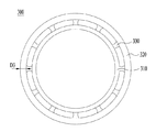
- 自転可能に構成されるディスク;
前記ディスクに配置され、上面に基板が装着され、前記ディスクが 自転することによって自転するとともに前記ディスクの中心を軸として公転する少なくとも一つのサセプタ;
前記サセプタの下部に結合し、中心が前記サセプタの中心と一致するように配置される金属リング;
前記ディスクの下部に前記ディスクの中心を基準に放射状に配置され、少なくとも一部が前記金属リングと上下方向に対向するように備えられるマグネット; 及び
前記ディスクを収容する収容部を備えるフレームを含み、
前記マグネットは複数の円筒状のマグネット片が一定間隔で放射状に配置されるように備えられ前記フレームに前記収容部の中心を基準に放射状に回転できないように配置されることを特徴とする、基板処理装置。 - 前記ディスク及び前記サセプタとそれぞれ接触するように配置されるベアリングをさらに含み、
前記ディスクが自転することによって前記金属リングは前記マグネットの磁気力によって自転し、これによって前記サセプタが自転することを特徴とする、請求項1に記載の基板処理装置。 - 前記サセプタの下部に突設され、前記金属リングと結合し、前記ベアリングを支持する第1支持部を備えることを特徴とする、請求項2に記載の基板処理装置。
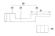
- 前記金属リングは、
前記第1支持部と結合する内側リング;
前記内側リングと結合する外側リング;及び
前記外側リングと前記内側リングの間に形成され、前記外側リングと前記内側リングを互いに結合させるリング結合部を含むことを特徴とする、請求項3に記載の基板処理装置。 - 前記外側リングは前記マグネットと上下方向に対向するように備えられ、
外側リングの幅は前記マグネットの幅より大きく形成されることを特徴とする、請求項4に記載の基板処理装置。 - 前記外側リングは前記マグネットと上下方向に対向するように備えられ、
前記外側リングは前記マグネットと対向する部位で前記マグネットを上下方向に全て覆う部位が存在するように構成されることを特徴とする、請求項4に記載の基板処理装置。 - 前記収容部の中心部に形成される通孔に挿入され、前記ディスクを自転させるシャフトと、下側で前記シャフトの上端と結合するとともに上側で前記ディスクと結合するディスク支持部を備えることを特徴とする、請求項1に記載の基板処理装置。
- 前記マグネットの直径に対する前記金属リングの直径の比に前記サセプタの自転速度が比例することを特徴とする、請求項1に記載の基板処理装置。
- 前記マグネットの直径はリング状に配置される前記マグネットの幅の中心間の距離を直径方向に測定した値であり、前記金属リングの直径は前記金属リングの幅の中心間の距離を直径方向に測定した値であることを特徴とする、請求項8に記載の基板処理装置。
- 前記金属リングは強磁性体でなることを特徴とする、請求項1に記載の基板処理装置。
- 前記ディスクの自転方向と前記サセプタの自転方向は同一であることを特徴とする、請求項1に記載の基板処理装置。
- 前記マグネットは前記ディスクの下部に前記ディスクの中心を基準に放射状に配置され、
前記マグネットの中心と前記金属リングの中心は互いに離隔するように備えられることを特徴とする、請求項1に記載の基板処理装置。 - 回転可能に構成されるディスク;
前記ディスクに配置され、上面に基板が装着され、前記ディスクが回転することによって自転するとともに前記ディスクの中心を軸として公転するサセプタ;
前記サセプタの下部に結合し、中心が前記サセプタの中心と一致するように配置される金属リング;及び
前記ディスクの下部に前記ディスクの中心を基準に複数の円筒状の片が一定間隔で放射状に配置され、前記金属リングと上下方向に対向するように備えられるマグネットを含み、
前記マグネットの直径に対する前記金属リングの直径の比に前記サセプタの自転速度が比例する、基板処理装置。 - 回転可能に構成されるディスク;
前記ディスクに配置され、上面に基板が装着され、前記ディスクが回転することによって自転するとともに前記ディスクの中心を軸として公転する少なくとも一つのサセプタ;
前記サセプタの外周面に結合する金属リング;及び
工程チャンバーの内壁に結合し、前記金属リングと軸方向に対向するように備えられるマグネットを含む、基板処理装置。 - ディスク中心を軸として前記ディスクが自転するディスクの自転段階;
前記ディスクが自転することによって前記ディスク中心を軸としてサセプタが公転するサセプタの公転段階;
前記サセプタの下部に結合する金属リングが、前記サセプタが公転することによって、前記ディスク中心を軸として公転する金属リングの公転段階;
上下方向に互いに対向する位置に置かれた前記金属リングと前記ディスクの中心を基準に複数の円筒状の片が一定間隔で放射状に配置されマグネットの間で前記マグネットが前記金属リングを引っ張る引力作用段階;及び
前記マグネットと前記金属リングの間に作用する引力によって前記金属リングが結合する前記サセプタが前記マグネットによって引っ張られて自転するサセプタの自転段階を含む、基板処理装置の作動方法。
Applications Claiming Priority (5)
| Application Number | Priority Date | Filing Date | Title |
|---|---|---|---|
| KR10-2015-0065094 | 2015-05-11 | ||
| KR20150065094 | 2015-05-11 | ||
| KR1020150097515A KR102508025B1 (ko) | 2015-05-11 | 2015-07-09 | 공정챔버 내부에 배치되는 기판 처리장치 및 그 작동방법 |
| KR10-2015-0097515 | 2015-07-09 | ||
| PCT/KR2016/004842 WO2016182299A1 (ko) | 2015-05-11 | 2016-05-10 | 공정챔버 내부에 배치되는 기판 처리장치 및 그 작동방법 |
Publications (3)
| Publication Number | Publication Date |
|---|---|
| JP2018515930A JP2018515930A (ja) | 2018-06-14 |
| JP2018515930A5 JP2018515930A5 (ja) | 2019-06-13 |
| JP6959696B2 true JP6959696B2 (ja) | 2021-11-05 |
Family
ID=57537945
Family Applications (1)
| Application Number | Title | Priority Date | Filing Date |
|---|---|---|---|
| JP2017559429A Active JP6959696B2 (ja) | 2015-05-11 | 2016-05-10 | 工程チャンバーの内部に配置される基板処理装置及びその作動方法 |
Country Status (5)
| Country | Link |
|---|---|
| US (2) | US10229849B2 (ja) |
| JP (1) | JP6959696B2 (ja) |
| KR (1) | KR102508025B1 (ja) |
| CN (2) | CN107667421B (ja) |
| TW (1) | TWI702670B (ja) |
Families Citing this family (3)
| Publication number | Priority date | Publication date | Assignee | Title |
|---|---|---|---|---|
| KR102508025B1 (ko) * | 2015-05-11 | 2023-03-10 | 주성엔지니어링(주) | 공정챔버 내부에 배치되는 기판 처리장치 및 그 작동방법 |
| KR20190140373A (ko) * | 2018-06-11 | 2019-12-19 | 캐논 톡키 가부시키가이샤 | 기판 회전 장치 및 기판 회전 방법 |
| CN110643949B (zh) * | 2019-10-29 | 2022-08-05 | 苏州华楷微电子有限公司 | 一种公转式半导体蒸发台的蒸发方法 |
Family Cites Families (18)
| Publication number | Priority date | Publication date | Assignee | Title |
|---|---|---|---|---|
| JPH01184277A (ja) * | 1988-01-18 | 1989-07-21 | Matsushita Electric Ind Co Ltd | 基板回転装置 |
| US5795448A (en) * | 1995-12-08 | 1998-08-18 | Sony Corporation | Magnetic device for rotating a substrate |
| JP4470680B2 (ja) * | 2004-10-12 | 2010-06-02 | 日立電線株式会社 | 気相成長装置 |
| KR101200372B1 (ko) * | 2005-06-15 | 2012-11-12 | 주성엔지니어링(주) | 박막 제조 장치 및 이를 이용한 박막 증착 방법 |
| KR100957525B1 (ko) | 2008-01-18 | 2010-05-11 | 이석태 | 반도체 및 평기판 회전장비용 전원장치 |
| JP4862002B2 (ja) * | 2008-02-27 | 2012-01-25 | 株式会社エムテーシー | 薄型基板回転処理装置 |
| KR101053047B1 (ko) | 2008-05-06 | 2011-08-01 | 삼성엘이디 주식회사 | 화학 기상 증착 장치 |
| JP5276388B2 (ja) * | 2008-09-04 | 2013-08-28 | 東京エレクトロン株式会社 | 成膜装置及び基板処理装置 |
| KR20100046962A (ko) * | 2008-10-28 | 2010-05-07 | 세메스 주식회사 | 기판 이송 장치 |
| KR20110116901A (ko) | 2010-04-20 | 2011-10-26 | 엘아이지에이디피 주식회사 | 서셉터 회전장치 및 이를 이용한 화학기상 증착장치 |
| US20120305036A1 (en) * | 2011-06-01 | 2012-12-06 | Lam Research Ag | Device for treating surfaces of wafer-shaped articles |
| KR20130061802A (ko) * | 2011-12-02 | 2013-06-12 | 주식회사 케이씨텍 | 회전하는 서셉터 포켓을 구비한 증착장치 |
| JP6017817B2 (ja) * | 2011-12-15 | 2016-11-02 | 住友化学株式会社 | 表面処理装置、表面処理方法、基板支持機構およびプログラム |
| JP6050944B2 (ja) * | 2012-04-05 | 2016-12-21 | 東京エレクトロン株式会社 | プラズマエッチング方法及びプラズマ処理装置 |
| CN103322996B (zh) * | 2013-06-20 | 2016-04-13 | 上海交通大学 | 电磁驱动静电检测体声波谐振三轴微陀螺及其制备方法 |
| JP6330630B2 (ja) * | 2014-11-13 | 2018-05-30 | 東京エレクトロン株式会社 | 成膜装置 |
| KR102508025B1 (ko) * | 2015-05-11 | 2023-03-10 | 주성엔지니어링(주) | 공정챔버 내부에 배치되는 기판 처리장치 및 그 작동방법 |
| JP6507953B2 (ja) * | 2015-09-08 | 2019-05-08 | 東京エレクトロン株式会社 | 基板処理装置及び基板処理方法 |
-
2015
- 2015-07-09 KR KR1020150097515A patent/KR102508025B1/ko active IP Right Grant
-
2016
- 2016-05-10 US US15/573,480 patent/US10229849B2/en active Active
- 2016-05-10 JP JP2017559429A patent/JP6959696B2/ja active Active
- 2016-05-10 CN CN201680027285.5A patent/CN107667421B/zh active Active
- 2016-05-10 CN CN202111132309.2A patent/CN114005783A/zh active Pending
- 2016-05-11 TW TW105114563A patent/TWI702670B/zh active
-
2019
- 2019-01-31 US US16/264,637 patent/US10818534B2/en active Active
Also Published As
| Publication number | Publication date |
|---|---|
| TW201701390A (zh) | 2017-01-01 |
| CN114005783A (zh) | 2022-02-01 |
| US20180144968A1 (en) | 2018-05-24 |
| CN107667421A (zh) | 2018-02-06 |
| US20190164801A1 (en) | 2019-05-30 |
| JP2018515930A (ja) | 2018-06-14 |
| KR20160132743A (ko) | 2016-11-21 |
| KR102508025B1 (ko) | 2023-03-10 |
| US10229849B2 (en) | 2019-03-12 |
| TWI702670B (zh) | 2020-08-21 |
| CN107667421B (zh) | 2021-10-01 |
| US10818534B2 (en) | 2020-10-27 |
Similar Documents
| Publication | Publication Date | Title |
|---|---|---|
| JP6959696B2 (ja) | 工程チャンバーの内部に配置される基板処理装置及びその作動方法 | |
| CN103104539B (zh) | 真空泵 | |
| JP2010193698A (ja) | スピンドルモーター | |
| CN101252296A (zh) | 电机 | |
| KR102446732B1 (ko) | 기판 처리장치 및 그 작동방법 | |
| JP2003061295A (ja) | スピンドルモータ | |
| JP2010178612A (ja) | スピンドルモーター | |
| JP4862002B2 (ja) | 薄型基板回転処理装置 | |
| JP2018515930A5 (ja) | ||
| KR101298768B1 (ko) | 원통형 스퍼터링 캐소드 장치 | |
| JPWO2014034504A1 (ja) | 基板ステージ及びそれを備えた基板処理装置 | |
| KR101136536B1 (ko) | 자석을 이용한 코팅 장치 | |
| KR101523944B1 (ko) | 웨이퍼 코팅장치 | |
| KR20160148157A (ko) | 공정챔버 내부에 배치되는 기판 처리장치 및 그 작동방법 | |
| CN215409984U (zh) | 一种承托机构 | |
| JP6410562B2 (ja) | 電動機 | |
| CN220827454U (zh) | 镀膜室及镀膜设备 | |
| JP2012164751A (ja) | 被膜形成装置および被膜形成方法 | |
| KR102510956B1 (ko) | 기판 처리장치 | |
| JP2012243386A (ja) | スピンドルモーター | |
| CN204311127U (zh) | 一种多功能离子镀轴承滚珠镀膜装置 | |
| TWI388690B (zh) | 鍍膜腔體結構及其鍍膜製程 | |
| TW202229146A (zh) | 用於旋轉基板之設備 | |
| JP5643664B2 (ja) | 電動ポンプ | |
| JP2014122371A (ja) | 蒸着装置 |
Legal Events
| Date | Code | Title | Description |
|---|---|---|---|
| A521 | Request for written amendment filed |
Free format text: JAPANESE INTERMEDIATE CODE: A523 Effective date: 20190510 |
|
| A621 | Written request for application examination |
Free format text: JAPANESE INTERMEDIATE CODE: A621 Effective date: 20190510 |
|
| A977 | Report on retrieval |
Free format text: JAPANESE INTERMEDIATE CODE: A971007 Effective date: 20200611 |
|
| A131 | Notification of reasons for refusal |
Free format text: JAPANESE INTERMEDIATE CODE: A131 Effective date: 20200714 |
|
| A521 | Request for written amendment filed |
Free format text: JAPANESE INTERMEDIATE CODE: A523 Effective date: 20201014 |
|
| A131 | Notification of reasons for refusal |
Free format text: JAPANESE INTERMEDIATE CODE: A131 Effective date: 20210406 |
|
| A521 | Request for written amendment filed |
Free format text: JAPANESE INTERMEDIATE CODE: A523 Effective date: 20210706 |
|
| TRDD | Decision of grant or rejection written | ||
| A01 | Written decision to grant a patent or to grant a registration (utility model) |
Free format text: JAPANESE INTERMEDIATE CODE: A01 Effective date: 20210907 |
|
| A61 | First payment of annual fees (during grant procedure) |
Free format text: JAPANESE INTERMEDIATE CODE: A61 Effective date: 20211005 |
|
| R150 | Certificate of patent or registration of utility model |
Ref document number: 6959696 Country of ref document: JP Free format text: JAPANESE INTERMEDIATE CODE: R150 |