JP6932056B2 - スイッチングレギュレータ - Google Patents
スイッチングレギュレータ Download PDFInfo
- Publication number
- JP6932056B2 JP6932056B2 JP2017196188A JP2017196188A JP6932056B2 JP 6932056 B2 JP6932056 B2 JP 6932056B2 JP 2017196188 A JP2017196188 A JP 2017196188A JP 2017196188 A JP2017196188 A JP 2017196188A JP 6932056 B2 JP6932056 B2 JP 6932056B2
- Authority
- JP
- Japan
- Prior art keywords
- voltage
- output
- circuit
- error
- input
- Prior art date
- Legal status (The legal status is an assumption and is not a legal conclusion. Google has not performed a legal analysis and makes no representation as to the accuracy of the status listed.)
- Active
Links
Images


Classifications
-
- H—ELECTRICITY
- H02—GENERATION; CONVERSION OR DISTRIBUTION OF ELECTRIC POWER
- H02M—APPARATUS FOR CONVERSION BETWEEN AC AND AC, BETWEEN AC AND DC, OR BETWEEN DC AND DC, AND FOR USE WITH MAINS OR SIMILAR POWER SUPPLY SYSTEMS; CONVERSION OF DC OR AC INPUT POWER INTO SURGE OUTPUT POWER; CONTROL OR REGULATION THEREOF
- H02M3/00—Conversion of dc power input into dc power output
- H02M3/02—Conversion of dc power input into dc power output without intermediate conversion into ac
- H02M3/04—Conversion of dc power input into dc power output without intermediate conversion into ac by static converters
- H02M3/10—Conversion of dc power input into dc power output without intermediate conversion into ac by static converters using discharge tubes with control electrode or semiconductor devices with control electrode
- H02M3/145—Conversion of dc power input into dc power output without intermediate conversion into ac by static converters using discharge tubes with control electrode or semiconductor devices with control electrode using devices of a triode or transistor type requiring continuous application of a control signal
- H02M3/155—Conversion of dc power input into dc power output without intermediate conversion into ac by static converters using discharge tubes with control electrode or semiconductor devices with control electrode using devices of a triode or transistor type requiring continuous application of a control signal using semiconductor devices only
- H02M3/156—Conversion of dc power input into dc power output without intermediate conversion into ac by static converters using discharge tubes with control electrode or semiconductor devices with control electrode using devices of a triode or transistor type requiring continuous application of a control signal using semiconductor devices only with automatic control of output voltage or current, e.g. switching regulators
- H02M3/158—Conversion of dc power input into dc power output without intermediate conversion into ac by static converters using discharge tubes with control electrode or semiconductor devices with control electrode using devices of a triode or transistor type requiring continuous application of a control signal using semiconductor devices only with automatic control of output voltage or current, e.g. switching regulators including plural semiconductor devices as final control devices for a single load
- H02M3/1588—Conversion of dc power input into dc power output without intermediate conversion into ac by static converters using discharge tubes with control electrode or semiconductor devices with control electrode using devices of a triode or transistor type requiring continuous application of a control signal using semiconductor devices only with automatic control of output voltage or current, e.g. switching regulators including plural semiconductor devices as final control devices for a single load comprising at least one synchronous rectifier element
-
- H—ELECTRICITY
- H02—GENERATION; CONVERSION OR DISTRIBUTION OF ELECTRIC POWER
- H02M—APPARATUS FOR CONVERSION BETWEEN AC AND AC, BETWEEN AC AND DC, OR BETWEEN DC AND DC, AND FOR USE WITH MAINS OR SIMILAR POWER SUPPLY SYSTEMS; CONVERSION OF DC OR AC INPUT POWER INTO SURGE OUTPUT POWER; CONTROL OR REGULATION THEREOF
- H02M3/00—Conversion of dc power input into dc power output
- H02M3/02—Conversion of dc power input into dc power output without intermediate conversion into ac
- H02M3/04—Conversion of dc power input into dc power output without intermediate conversion into ac by static converters
- H02M3/10—Conversion of dc power input into dc power output without intermediate conversion into ac by static converters using discharge tubes with control electrode or semiconductor devices with control electrode
- H02M3/145—Conversion of dc power input into dc power output without intermediate conversion into ac by static converters using discharge tubes with control electrode or semiconductor devices with control electrode using devices of a triode or transistor type requiring continuous application of a control signal
- H02M3/155—Conversion of dc power input into dc power output without intermediate conversion into ac by static converters using discharge tubes with control electrode or semiconductor devices with control electrode using devices of a triode or transistor type requiring continuous application of a control signal using semiconductor devices only
- H02M3/156—Conversion of dc power input into dc power output without intermediate conversion into ac by static converters using discharge tubes with control electrode or semiconductor devices with control electrode using devices of a triode or transistor type requiring continuous application of a control signal using semiconductor devices only with automatic control of output voltage or current, e.g. switching regulators
- H02M3/158—Conversion of dc power input into dc power output without intermediate conversion into ac by static converters using discharge tubes with control electrode or semiconductor devices with control electrode using devices of a triode or transistor type requiring continuous application of a control signal using semiconductor devices only with automatic control of output voltage or current, e.g. switching regulators including plural semiconductor devices as final control devices for a single load
-
- G—PHYSICS
- G05—CONTROLLING; REGULATING
- G05F—SYSTEMS FOR REGULATING ELECTRIC OR MAGNETIC VARIABLES
- G05F1/00—Automatic systems in which deviations of an electric quantity from one or more predetermined values are detected at the output of the system and fed back to a device within the system to restore the detected quantity to its predetermined value or values, i.e. retroactive systems
- G05F1/10—Regulating voltage or current
- G05F1/46—Regulating voltage or current wherein the variable actually regulated by the final control device is dc
- G05F1/461—Regulating voltage or current wherein the variable actually regulated by the final control device is dc using an operational amplifier as final control device
-
- H—ELECTRICITY
- H02—GENERATION; CONVERSION OR DISTRIBUTION OF ELECTRIC POWER
- H02M—APPARATUS FOR CONVERSION BETWEEN AC AND AC, BETWEEN AC AND DC, OR BETWEEN DC AND DC, AND FOR USE WITH MAINS OR SIMILAR POWER SUPPLY SYSTEMS; CONVERSION OF DC OR AC INPUT POWER INTO SURGE OUTPUT POWER; CONTROL OR REGULATION THEREOF
- H02M1/00—Details of apparatus for conversion
- H02M1/0045—Converters combining the concepts of switch-mode regulation and linear regulation, e.g. linear pre-regulator to switching converter, linear and switching converter in parallel, same converter or same transistor operating either in linear or switching mode
-
- H—ELECTRICITY
- H02—GENERATION; CONVERSION OR DISTRIBUTION OF ELECTRIC POWER
- H02M—APPARATUS FOR CONVERSION BETWEEN AC AND AC, BETWEEN AC AND DC, OR BETWEEN DC AND DC, AND FOR USE WITH MAINS OR SIMILAR POWER SUPPLY SYSTEMS; CONVERSION OF DC OR AC INPUT POWER INTO SURGE OUTPUT POWER; CONTROL OR REGULATION THEREOF
- H02M1/00—Details of apparatus for conversion
- H02M1/08—Circuits specially adapted for the generation of control voltages for semiconductor devices incorporated in static converters
- H02M1/088—Circuits specially adapted for the generation of control voltages for semiconductor devices incorporated in static converters for the simultaneous control of series or parallel connected semiconductor devices
-
- H—ELECTRICITY
- H02—GENERATION; CONVERSION OR DISTRIBUTION OF ELECTRIC POWER
- H02M—APPARATUS FOR CONVERSION BETWEEN AC AND AC, BETWEEN AC AND DC, OR BETWEEN DC AND DC, AND FOR USE WITH MAINS OR SIMILAR POWER SUPPLY SYSTEMS; CONVERSION OF DC OR AC INPUT POWER INTO SURGE OUTPUT POWER; CONTROL OR REGULATION THEREOF
- H02M3/00—Conversion of dc power input into dc power output
- H02M3/02—Conversion of dc power input into dc power output without intermediate conversion into ac
- H02M3/04—Conversion of dc power input into dc power output without intermediate conversion into ac by static converters
- H02M3/10—Conversion of dc power input into dc power output without intermediate conversion into ac by static converters using discharge tubes with control electrode or semiconductor devices with control electrode
- H02M3/145—Conversion of dc power input into dc power output without intermediate conversion into ac by static converters using discharge tubes with control electrode or semiconductor devices with control electrode using devices of a triode or transistor type requiring continuous application of a control signal
- H02M3/155—Conversion of dc power input into dc power output without intermediate conversion into ac by static converters using discharge tubes with control electrode or semiconductor devices with control electrode using devices of a triode or transistor type requiring continuous application of a control signal using semiconductor devices only
- H02M3/156—Conversion of dc power input into dc power output without intermediate conversion into ac by static converters using discharge tubes with control electrode or semiconductor devices with control electrode using devices of a triode or transistor type requiring continuous application of a control signal using semiconductor devices only with automatic control of output voltage or current, e.g. switching regulators
- H02M3/1563—Conversion of dc power input into dc power output without intermediate conversion into ac by static converters using discharge tubes with control electrode or semiconductor devices with control electrode using devices of a triode or transistor type requiring continuous application of a control signal using semiconductor devices only with automatic control of output voltage or current, e.g. switching regulators without using an external clock
-
- H—ELECTRICITY
- H02—GENERATION; CONVERSION OR DISTRIBUTION OF ELECTRIC POWER
- H02M—APPARATUS FOR CONVERSION BETWEEN AC AND AC, BETWEEN AC AND DC, OR BETWEEN DC AND DC, AND FOR USE WITH MAINS OR SIMILAR POWER SUPPLY SYSTEMS; CONVERSION OF DC OR AC INPUT POWER INTO SURGE OUTPUT POWER; CONTROL OR REGULATION THEREOF
- H02M1/00—Details of apparatus for conversion
- H02M1/0003—Details of control, feedback or regulation circuits
- H02M1/0012—Control circuits using digital or numerical techniques
-
- H—ELECTRICITY
- H02—GENERATION; CONVERSION OR DISTRIBUTION OF ELECTRIC POWER
- H02M—APPARATUS FOR CONVERSION BETWEEN AC AND AC, BETWEEN AC AND DC, OR BETWEEN DC AND DC, AND FOR USE WITH MAINS OR SIMILAR POWER SUPPLY SYSTEMS; CONVERSION OF DC OR AC INPUT POWER INTO SURGE OUTPUT POWER; CONTROL OR REGULATION THEREOF
- H02M1/00—Details of apparatus for conversion
- H02M1/0003—Details of control, feedback or regulation circuits
- H02M1/0025—Arrangements for modifying reference values, feedback values or error values in the control loop of a converter
-
- H—ELECTRICITY
- H02—GENERATION; CONVERSION OR DISTRIBUTION OF ELECTRIC POWER
- H02M—APPARATUS FOR CONVERSION BETWEEN AC AND AC, BETWEEN AC AND DC, OR BETWEEN DC AND DC, AND FOR USE WITH MAINS OR SIMILAR POWER SUPPLY SYSTEMS; CONVERSION OF DC OR AC INPUT POWER INTO SURGE OUTPUT POWER; CONTROL OR REGULATION THEREOF
- H02M3/00—Conversion of dc power input into dc power output
- H02M3/02—Conversion of dc power input into dc power output without intermediate conversion into ac
- H02M3/04—Conversion of dc power input into dc power output without intermediate conversion into ac by static converters
- H02M3/10—Conversion of dc power input into dc power output without intermediate conversion into ac by static converters using discharge tubes with control electrode or semiconductor devices with control electrode
- H02M3/145—Conversion of dc power input into dc power output without intermediate conversion into ac by static converters using discharge tubes with control electrode or semiconductor devices with control electrode using devices of a triode or transistor type requiring continuous application of a control signal
- H02M3/155—Conversion of dc power input into dc power output without intermediate conversion into ac by static converters using discharge tubes with control electrode or semiconductor devices with control electrode using devices of a triode or transistor type requiring continuous application of a control signal using semiconductor devices only
- H02M3/156—Conversion of dc power input into dc power output without intermediate conversion into ac by static converters using discharge tubes with control electrode or semiconductor devices with control electrode using devices of a triode or transistor type requiring continuous application of a control signal using semiconductor devices only with automatic control of output voltage or current, e.g. switching regulators
- H02M3/1566—Conversion of dc power input into dc power output without intermediate conversion into ac by static converters using discharge tubes with control electrode or semiconductor devices with control electrode using devices of a triode or transistor type requiring continuous application of a control signal using semiconductor devices only with automatic control of output voltage or current, e.g. switching regulators with means for compensating against rapid load changes, e.g. with auxiliary current source, with dual mode control or with inductance variation
Description
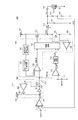
101、102、501 電源端子
103、502 接地端子
110、112、510、512 基準電圧源
111、163、511 誤差増幅回路
113、513 PFM比較回路
114、514 発振回路
120、520 電流電圧変換回路
121、521 スロープ電圧生成回路
122、522 PWM比較回路
123、523 制御回路
124、524 逆流検出回路
130、530 PMOSトランジスタ
131、164、531 NMOSトランジスタ
140、540 インダクタ
141、541 容量
142、542 出力端子
143、144、543、544 抵抗
150、550 PWM変換回路
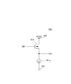
160 クランプ回路
161 バッファ回路
162、262 定電圧発生部
Claims (4)
- 第1の電源端子に供給される電源電圧から出力端子に所定の出力電圧を生成するスイッチングレギュレータであって、
一端が前記出力端子に接続されたインダクタと、
前記第1の電源端子と前記インダクタの他端との間に接続されたスイッチング素子と、
前記出力電圧に基づく電圧と第1の基準電圧との差を増幅し、第1の誤差電圧を出力する第1の誤差増幅回路と、
第1の入力ノードに入力される前記第1の誤差電圧と第2の入力ノードに入力される第2の基準電圧とに基づき出力ノードに第2の誤差電圧を生成するクランプ回路と、
第1の入力端子に入力される前記第2の誤差電圧と第2の入力端子に入力される前記第2の基準電圧とを比較し、第1のレベルまたは第2のレベルの比較結果信号を出力するPFM比較回路と、
前記比較結果信号が前記第1のレベルのとき所定周波数のクロック信号を出力し、前記比較結果信号が前記第2のレベルのとき前記クロック信号の出力を停止する発振回路と、
前記第2の誤差電圧と前記発振回路の出力とに基づいて前記スイッチング素子を所望のパルス幅でオン・オフするPWM変換回路とを備え、
前記クランプ回路は、入力が前記第1の入力ノードに接続され、出力が前記出力ノードに接続されたバッファ回路と、
一端が前記出力ノードに接続され、定電圧を発生する定電圧発生部と、
前記定電圧発生部の他端の電圧と前記第2の基準電圧との差を増幅する第2の誤差増幅回路と、
第2の電源端子と前記第1の入力ノードとの間に接続され、ゲートが前記第2の誤差増幅回路の出力に接続されたMOSトランジスタとを有し、
前記第2の誤差電圧の下限値を前記第2の基準電圧の電圧値から前記定電圧を減算した電圧値にクランプすることを特徴とするスイッチングレギュレータ。 - 前記定電圧発生部は、前記第2の誤差増幅回路の前記定電圧発生部の他端の電圧が入力される端子と前記出力ノードとの間に接続されていることを特徴とする請求項1に記載のスイッチングレギュレータ。
- 前記定電圧発生部は、前記バッファ回路の出力と前記出力ノードとの間に接続されていることを特徴とする請求項1に記載のスイッチングレギュレータ。
- 前記バッファ回路は、ソースフォロワ回路で構成されていることを特徴とする請求項1乃至3のいずれか一項に記載のスイッチングレギュレータ。
Priority Applications (5)
| Application Number | Priority Date | Filing Date | Title |
|---|---|---|---|
| JP2017196188A JP6932056B2 (ja) | 2017-10-06 | 2017-10-06 | スイッチングレギュレータ |
| TW107133441A TWI784054B (zh) | 2017-10-06 | 2018-09-21 | 開關穩壓器 |
| CN201811121320.7A CN109639142A (zh) | 2017-10-06 | 2018-09-26 | 开关调节器 |
| US16/151,954 US10468989B2 (en) | 2017-10-06 | 2018-10-04 | Switching regulator including a clamp circuit |
| KR1020180118290A KR102560435B1 (ko) | 2017-10-06 | 2018-10-04 | 스위칭 레귤레이터 |
Applications Claiming Priority (1)
| Application Number | Priority Date | Filing Date | Title |
|---|---|---|---|
| JP2017196188A JP6932056B2 (ja) | 2017-10-06 | 2017-10-06 | スイッチングレギュレータ |
Publications (3)
| Publication Number | Publication Date |
|---|---|
| JP2019071715A JP2019071715A (ja) | 2019-05-09 |
| JP2019071715A5 JP2019071715A5 (ja) | 2020-11-12 |
| JP6932056B2 true JP6932056B2 (ja) | 2021-09-08 |
Family
ID=65993519
Family Applications (1)
| Application Number | Title | Priority Date | Filing Date |
|---|---|---|---|
| JP2017196188A Active JP6932056B2 (ja) | 2017-10-06 | 2017-10-06 | スイッチングレギュレータ |
Country Status (5)
| Country | Link |
|---|---|
| US (1) | US10468989B2 (ja) |
| JP (1) | JP6932056B2 (ja) |
| KR (1) | KR102560435B1 (ja) |
| CN (1) | CN109639142A (ja) |
| TW (1) | TWI784054B (ja) |
Families Citing this family (4)
| Publication number | Priority date | Publication date | Assignee | Title |
|---|---|---|---|---|
| US10726881B1 (en) * | 2019-04-08 | 2020-07-28 | Texas Instruments Incorporated | Supply voltage clamping for improved power supply rejection ratio |
| KR102238846B1 (ko) * | 2019-11-05 | 2021-04-09 | 현대모비스 주식회사 | Dc-dc 컨버터 전류모드 제어용 보조장치 |
| TWI749906B (zh) * | 2020-11-25 | 2021-12-11 | 台達電子工業股份有限公司 | 電源系統及其適用之脈寬調變方法 |
| CN114552983A (zh) | 2020-11-25 | 2022-05-27 | 台达电子工业股份有限公司 | 电源系统及其适用的脉宽调制方法 |
Family Cites Families (27)
| Publication number | Priority date | Publication date | Assignee | Title |
|---|---|---|---|---|
| JP2005210335A (ja) * | 2004-01-22 | 2005-08-04 | Nec Electronics Corp | 相関二重サンプリング回路、信号処理回路及び固体撮像装置 |
| TW200525869A (en) * | 2004-01-28 | 2005-08-01 | Renesas Tech Corp | Switching power supply and semiconductor IC |
| JP4578198B2 (ja) * | 2004-09-30 | 2010-11-10 | 株式会社リコー | スイッチングレギュレータ |
| US7382114B2 (en) * | 2005-06-07 | 2008-06-03 | Intersil Americas Inc. | PFM-PWM DC-DC converter providing DC offset correction to PWM error amplifier and equalizing regulated voltage conditions when transitioning between PFM and PWM modes |
| US7378827B2 (en) * | 2005-08-24 | 2008-05-27 | Micrel, Incorporated | Analog internal soft-start and clamp circuit for switching regulator |
| WO2007080777A1 (ja) * | 2006-01-10 | 2007-07-19 | Rohm Co., Ltd. | 電源装置及びこれを備えた電子機器 |
| JP4836624B2 (ja) * | 2006-03-23 | 2011-12-14 | 株式会社リコー | スイッチングレギュレータ |
| GB2437556B (en) * | 2006-04-26 | 2011-03-23 | Wolfson Microelectronics Plc | Improvements in switching regulator circuits |
| US20090079408A1 (en) * | 2007-09-21 | 2009-03-26 | Nexem, Inc. | Voltage mode pwmff-pfm/skip combo controller |
| JP4618339B2 (ja) * | 2008-06-20 | 2011-01-26 | ミツミ電機株式会社 | Dc−dcコンバータ |
| JP5211959B2 (ja) * | 2008-09-12 | 2013-06-12 | 株式会社リコー | Dc−dcコンバータ |
| JP5504685B2 (ja) * | 2009-04-27 | 2014-05-28 | 株式会社リコー | スイッチングレギュレータ及びその動作制御方法 |
| US8169205B2 (en) * | 2009-05-26 | 2012-05-01 | Silergy Technology | Control for regulator fast transient response and low EMI noise |
| JP5785814B2 (ja) * | 2011-08-18 | 2015-09-30 | ローム株式会社 | スイッチング電源の制御回路、制御方法ならびにそれを用いたスイッチング電源および電子機器 |
| JP2013168880A (ja) * | 2012-02-16 | 2013-08-29 | Sony Corp | 比較器、ad変換器、固体撮像装置、カメラシステム、および電子機器 |
| JP6168793B2 (ja) * | 2013-03-04 | 2017-07-26 | エスアイアイ・セミコンダクタ株式会社 | スイッチングレギュレータ及び電子機器 |
| JP6161339B2 (ja) * | 2013-03-13 | 2017-07-12 | ラピスセミコンダクタ株式会社 | 昇圧型スイッチングレギュレータおよび半導体装置 |
| US9287776B2 (en) * | 2013-07-30 | 2016-03-15 | Texas Instruments Incorporated | Low power switching mode regulator having automatic PFM and PWM operation |
| JP6211916B2 (ja) * | 2013-12-24 | 2017-10-11 | エスアイアイ・セミコンダクタ株式会社 | スイッチングレギュレータ |
| JP6257363B2 (ja) * | 2014-02-06 | 2018-01-10 | エスアイアイ・セミコンダクタ株式会社 | スイッチングレギュレータ制御回路及びスイッチングレギュレータ |
| JP6253436B2 (ja) * | 2014-02-13 | 2017-12-27 | エスアイアイ・セミコンダクタ株式会社 | Dc/dcコンバータ |
| US9667145B1 (en) * | 2015-02-11 | 2017-05-30 | Marvell International Ltd. | Fast transient response for switching regulators |
| CN104993701B (zh) * | 2015-07-22 | 2017-05-24 | 无锡中感微电子股份有限公司 | 一种pwm/pfm控制电路 |
| DE102015219307B4 (de) * | 2015-10-06 | 2018-07-19 | Dialog Semiconductor (Uk) Limited | Schaltleistungswandler mit einer Strombegrenzungsschaltung |
| US10551859B2 (en) * | 2016-05-17 | 2020-02-04 | Texas Instruments Incorporated | Methods and apparatus for overshoot, undershoot and delay reduction of a voltage regulator output by dynamically offsetting a reference voltage |
| CN106130325B (zh) * | 2016-07-13 | 2019-06-18 | 成都芯源系统有限公司 | 一种降噪开关变换器以及控制电路和方法 |
| US10148177B2 (en) * | 2016-12-28 | 2018-12-04 | Texas Instruments Incorporated | Multiphase converter with phase interleaving |
-
2017
- 2017-10-06 JP JP2017196188A patent/JP6932056B2/ja active Active
-
2018
- 2018-09-21 TW TW107133441A patent/TWI784054B/zh active
- 2018-09-26 CN CN201811121320.7A patent/CN109639142A/zh active Pending
- 2018-10-04 US US16/151,954 patent/US10468989B2/en active Active
- 2018-10-04 KR KR1020180118290A patent/KR102560435B1/ko active IP Right Grant
Also Published As
| Publication number | Publication date |
|---|---|
| JP2019071715A (ja) | 2019-05-09 |
| US20190109541A1 (en) | 2019-04-11 |
| KR102560435B1 (ko) | 2023-07-27 |
| KR20190039868A (ko) | 2019-04-16 |
| US10468989B2 (en) | 2019-11-05 |
| CN109639142A (zh) | 2019-04-16 |
| TWI784054B (zh) | 2022-11-21 |
| TW201923504A (zh) | 2019-06-16 |
Similar Documents
| Publication | Publication Date | Title |
|---|---|---|
| JP6932056B2 (ja) | スイッチングレギュレータ | |
| JP5664327B2 (ja) | Dc−dcコンバータの制御装置 | |
| US20050156658A1 (en) | DC-DC converter | |
| JP7101590B2 (ja) | スイッチングレギュレータ | |
| KR20070094486A (ko) | 비절연 강압형 dc-dc 컨버터 | |
| JP6257363B2 (ja) | スイッチングレギュレータ制御回路及びスイッチングレギュレータ | |
| JP2010288334A (ja) | スイッチング電源装置及び半導体装置 | |
| JP2009033883A (ja) | スイッチングレギュレータ及びその動作制御方法 | |
| US9647540B2 (en) | Timing generator and timing signal generation method for power converter | |
| US9467044B2 (en) | Timing generator and timing signal generation method for power converter | |
| JP6912300B2 (ja) | スイッチングレギュレータ | |
| JP6153732B2 (ja) | スイッチングレギュレータ | |
| JP3576526B2 (ja) | Dc/dcコンバータ | |
| JP5130944B2 (ja) | Dc−dcコンバータおよび電源制御用半導体集積回路 | |
| JP4464263B2 (ja) | スイッチング電源装置 | |
| JP6654548B2 (ja) | スイッチング電源装置 | |
| JP2005057954A (ja) | 昇降圧自動切換え回路 | |
| JP6940384B2 (ja) | スイッチングレギュレータ | |
| JP2010063290A (ja) | 電源制御回路 | |
| JP2002165442A (ja) | デューティ制御装置および直流―直流変換装置 | |
| JP2005304273A (ja) | スイッチング電源用制御回路 |
Legal Events
| Date | Code | Title | Description |
|---|---|---|---|
| A521 | Request for written amendment filed |
Free format text: JAPANESE INTERMEDIATE CODE: A523 Effective date: 20200930 |
|
| A621 | Written request for application examination |
Free format text: JAPANESE INTERMEDIATE CODE: A621 Effective date: 20200930 |
|
| A977 | Report on retrieval |
Free format text: JAPANESE INTERMEDIATE CODE: A971007 Effective date: 20210630 |
|
| A131 | Notification of reasons for refusal |
Free format text: JAPANESE INTERMEDIATE CODE: A131 Effective date: 20210706 |
|
| A521 | Request for written amendment filed |
Free format text: JAPANESE INTERMEDIATE CODE: A523 Effective date: 20210727 |
|
| TRDD | Decision of grant or rejection written | ||
| A01 | Written decision to grant a patent or to grant a registration (utility model) |
Free format text: JAPANESE INTERMEDIATE CODE: A01 Effective date: 20210810 |
|
| A61 | First payment of annual fees (during grant procedure) |
Free format text: JAPANESE INTERMEDIATE CODE: A61 Effective date: 20210817 |
|
| R150 | Certificate of patent or registration of utility model |
Ref document number: 6932056 Country of ref document: JP Free format text: JAPANESE INTERMEDIATE CODE: R150 |
|
| S531 | Written request for registration of change of domicile |
Free format text: JAPANESE INTERMEDIATE CODE: R313531 |
|
| R350 | Written notification of registration of transfer |
Free format text: JAPANESE INTERMEDIATE CODE: R350 |