JP6869355B2 - Flexible circuit board and frame assembly containing it - Google Patents
Flexible circuit board and frame assembly containing it Download PDFInfo
- Publication number
- JP6869355B2 JP6869355B2 JP2019536176A JP2019536176A JP6869355B2 JP 6869355 B2 JP6869355 B2 JP 6869355B2 JP 2019536176 A JP2019536176 A JP 2019536176A JP 2019536176 A JP2019536176 A JP 2019536176A JP 6869355 B2 JP6869355 B2 JP 6869355B2
- Authority
- JP
- Japan
- Prior art keywords
- connecting circuit
- bus bar
- circuit board
- frame assembly
- flexible circuit
- Prior art date
- Legal status (The legal status is an assumption and is not a legal conclusion. Google has not performed a legal analysis and makes no representation as to the accuracy of the status listed.)
- Active
Links
Images


Classifications
-
- H—ELECTRICITY
- H01—ELECTRIC ELEMENTS
- H01M—PROCESSES OR MEANS, e.g. BATTERIES, FOR THE DIRECT CONVERSION OF CHEMICAL ENERGY INTO ELECTRICAL ENERGY
- H01M10/00—Secondary cells; Manufacture thereof
- H01M10/42—Methods or arrangements for servicing or maintenance of secondary cells or secondary half-cells
- H01M10/425—Structural combination with electronic components, e.g. electronic circuits integrated to the outside of the casing
-
- H—ELECTRICITY
- H01—ELECTRIC ELEMENTS
- H01M—PROCESSES OR MEANS, e.g. BATTERIES, FOR THE DIRECT CONVERSION OF CHEMICAL ENERGY INTO ELECTRICAL ENERGY
- H01M10/00—Secondary cells; Manufacture thereof
- H01M10/42—Methods or arrangements for servicing or maintenance of secondary cells or secondary half-cells
- H01M10/48—Accumulators combined with arrangements for measuring, testing or indicating the condition of cells, e.g. the level or density of the electrolyte
- H01M10/482—Accumulators combined with arrangements for measuring, testing or indicating the condition of cells, e.g. the level or density of the electrolyte for several batteries or cells simultaneously or sequentially
-
- H—ELECTRICITY
- H01—ELECTRIC ELEMENTS
- H01M—PROCESSES OR MEANS, e.g. BATTERIES, FOR THE DIRECT CONVERSION OF CHEMICAL ENERGY INTO ELECTRICAL ENERGY
- H01M50/00—Constructional details or processes of manufacture of the non-active parts of electrochemical cells other than fuel cells, e.g. hybrid cells
- H01M50/50—Current conducting connections for cells or batteries
- H01M50/528—Fixed electrical connections, i.e. not intended for disconnection
-
- H—ELECTRICITY
- H01—ELECTRIC ELEMENTS
- H01M—PROCESSES OR MEANS, e.g. BATTERIES, FOR THE DIRECT CONVERSION OF CHEMICAL ENERGY INTO ELECTRICAL ENERGY
- H01M50/00—Constructional details or processes of manufacture of the non-active parts of electrochemical cells other than fuel cells, e.g. hybrid cells
- H01M50/50—Current conducting connections for cells or batteries
- H01M50/543—Terminals
- H01M50/564—Terminals characterised by their manufacturing process
- H01M50/567—Terminals characterised by their manufacturing process by fixing means, e.g. screws, rivets or bolts
-
- H—ELECTRICITY
- H01—ELECTRIC ELEMENTS
- H01M—PROCESSES OR MEANS, e.g. BATTERIES, FOR THE DIRECT CONVERSION OF CHEMICAL ENERGY INTO ELECTRICAL ENERGY
- H01M50/00—Constructional details or processes of manufacture of the non-active parts of electrochemical cells other than fuel cells, e.g. hybrid cells
- H01M50/20—Mountings; Secondary casings or frames; Racks, modules or packs; Suspension devices; Shock absorbers; Transport or carrying devices; Holders
- H01M50/204—Racks, modules or packs for multiple batteries or multiple cells
-
- H—ELECTRICITY
- H05—ELECTRIC TECHNIQUES NOT OTHERWISE PROVIDED FOR
- H05K—PRINTED CIRCUITS; CASINGS OR CONSTRUCTIONAL DETAILS OF ELECTRIC APPARATUS; MANUFACTURE OF ASSEMBLAGES OF ELECTRICAL COMPONENTS
- H05K1/00—Printed circuits
- H05K1/18—Printed circuits structurally associated with non-printed electric components
Description
本開示は、軟性回路基板及びこれを含むフレーム組立体に関するものである。 The present disclosure relates to a flexible circuit board and a frame assembly including the same.
二次電池は、モバイル機器、補助電力装置などに広範囲に用いられている。また、二次電池は、従来ガソリン車両やディーゼル車両が有する大気汚染などの各種問題を解決するための代案として提示された電気自動車、ハイブリッド電気自動車、プラグインハイブリッド電気自動車などの主な原動力としても注目されている。 Secondary batteries are widely used in mobile devices, auxiliary power units, and the like. In addition, the secondary battery is also used as the main driving force for electric vehicles, hybrid electric vehicles, plug-in hybrid electric vehicles, etc., which have been presented as alternatives for solving various problems such as air pollution that conventional gasoline vehicles and diesel vehicles have. Attention has been paid.
電気自動車などに用いられる二次電池は、高出力大容量バッテリーの必要性により、複数個のバッテリーセルを積層させた後にこれを電気的に直列及び並列連結したバッテリーモジュールが用いられる。このようなバッテリーモジュールは、バッテリーセルの積層された程度により必要な高出力を提供することができるという長所があるが、バッテリーセルが積層された状態で用いられ、一部のバッテリーセルで過電圧、過電流、過発熱などの現象が生じ得る。 As a secondary battery used in an electric vehicle or the like, a battery module in which a plurality of battery cells are laminated and then electrically connected in series or in parallel is used due to the need for a high-output large-capacity battery. Such a battery module has an advantage that it can provide the required high output depending on the degree of stacking of the battery cells, but it is used in a state where the battery cells are stacked, and some battery cells are overvoltage. Phenomena such as overcurrent and overheating may occur.
このような形状は、バッテリーモジュールの安定性や作動効率などに影響を及ぼすため、これを予め検出するための手段が要請される。従って、バッテリーモジュールは、バッテリーセルに連結される回路基板を用いて各バッテリーセルの電圧をセンシングし、これをバスバーを介してBMS(Battery Management System)に電気的情報として伝達して、各バッテリーセルの過電圧、過電流、過発熱などの現象を検出し、これによる追加の損傷を防止する。 Since such a shape affects the stability and operating efficiency of the battery module, a means for detecting this in advance is required. Therefore, the battery module senses the voltage of each battery cell using the circuit board connected to the battery cell, transmits this to the BMS (Battery Management System) as electrical information via the bus bar, and each battery cell. Detects phenomena such as overvoltage, overcurrent, and overheating, and prevents additional damage caused by them.
一方、薄い絶縁層の間に銅箔が積層されて形成される軟性回路基板は、重さが軽く、占有空間が小さく、所望の形状に応じて裁断して用いることができる長所があるため、最近、多様な分野で用いられている。従って、車両のフレーム組立体においても車両の軽量化及び燃費改善のために、バッテリーセルの電圧をセンシングするために軟性回路基板を用いるための多様な研究が進行中である。 On the other hand, a flexible circuit board formed by laminating copper foil between thin insulating layers has advantages that it is light in weight, occupies a small space, and can be cut and used according to a desired shape. Recently, it has been used in various fields. Therefore, various studies are underway to use a flexible circuit board for sensing the voltage of the battery cell in order to reduce the weight of the vehicle and improve the fuel efficiency in the frame assembly of the vehicle.
本開示の実施例は、セル組立体を固定するためのフレーム組立体に用いられる軟性回路基板を提供する。また、生産過程の歩留まりを向上させて、組み立て過程で生じ得る破損現象を防止し、作業性を向上させることができる軟性回路基板の構造を提供する。 The embodiments of the present disclosure provide a flexible circuit board used in a frame assembly for fixing a cell assembly. Further, the present invention provides a structure of a flexible circuit board capable of improving the yield in the production process, preventing a breakage phenomenon that may occur in the assembly process, and improving workability.
本開示の一実施例によるバスバーが結合されたフレームに設けられる軟性回路基板において、バンド状の中心部;中心部の両端部に形成されて、互いに対向するように配置される第1連結回路部;第1連結回路部から中心部と並ぶように延びた第2連結回路部;及び第1連結回路部及び第2連結回路部のそれぞれから延びてバスバーに連結される第3連結回路部を含み、第2連結回路部が第1連結回路部の一側に折れる場合、端面方向で互いに重なるように配置された第1連結回路部の一部及び第2連結回路部の一部を含む重ね合わせ部が形成され、重ね合わせ部が形成される場合、第2連結回路部は第1連結回路部と同一線上に配置され得る。 In the flexible circuit board provided in the frame to which the bus bar is coupled according to the embodiment of the present disclosure, a band-shaped central portion; a first connecting circuit portion formed at both ends of the central portion and arranged so as to face each other. Includes a second connected circuit section that extends from the first connected circuit section so as to line up with the central portion; and a third connected circuit section that extends from each of the first connected circuit section and the second connected circuit section and is connected to the bus bar. , When the second connection circuit part is folded to one side of the first connection circuit part, the overlap including a part of the first connection circuit part and a part of the second connection circuit part arranged so as to overlap each other in the end face direction. When the portions are formed and the overlapping portions are formed, the second connecting circuit portion may be arranged on the same line as the first connecting circuit portion.
一実施例によると、第2連結回路部は、第1連結回路部の両端部にそれぞれ形成され、第2連結回路部が第1ベンディングラインに沿って第1連結回路部に向かって折れて形成される第1重ね合わせ部;及び第2連結回路部が第2ベンディングラインに沿って第1連結回路部の長さ方向に折れ曲がるように折れて形成される第2重ね合わせ部を含むことができる。 According to one embodiment, the second connecting circuit section is formed at both ends of the first connecting circuit section, and the second connecting circuit section is formed by bending toward the first connecting circuit section along the first bending line. The first overlapping portion to be formed; and the second overlapping portion formed by bending the second connecting circuit portion along the second bending line in the length direction of the first connecting circuit portion can be included. ..
一実施例によると、第1ベンディングラインは第1連結回路部と並んで形成され、第2ベンディングラインは第1ベンディングラインに対して所定の角度に傾くように形成され得る。 According to one embodiment, the first bending line may be formed alongside the first connecting circuit section, and the second bending line may be formed so as to be inclined at a predetermined angle with respect to the first bending line.
一実施例によると、第1重ね合わせ部及び第2重ね合わせ部を構成する第2連結回路部の部分の間は、上側及び下側に対して固定力を提供する接着剤により密着固定され得る。 According to one embodiment, the first overlapping portion and the second connecting circuit portion constituting the second overlapping portion can be closely fixed by an adhesive that provides a fixing force to the upper side and the lower side. ..
一実施例によると、接着剤は、両面テープまたは両面パッドであることを特徴とすることができる。 According to one embodiment, the adhesive can be characterized by being a double-sided tape or a double-sided pad.
一実施例によると、第1連結回路部に形成された第3連結回路部は、互いに離隔するように複数個で形成され、第1連結回路部と第2連結回路部が同一線上に位置する場合、第2連結回路部に形成された第3連結回路部が第1連結回路部に形成された第3連結回路部と一列に配置され得る。 According to one embodiment, a plurality of third connected circuit portions formed in the first connected circuit portion are formed so as to be separated from each other, and the first connected circuit portion and the second connected circuit portion are located on the same line. In this case, the third connecting circuit section formed in the second connecting circuit section may be arranged in a row with the third connecting circuit section formed in the first connecting circuit section.
一実施例によると、中心部から外側に延びて形成される温度センシング部をさらに含むことができる。 According to one embodiment, a temperature sensing portion formed extending outward from the central portion can be further included.
一実施例によると、第3連結回路部は、基板層及び基板層の一面を露出させるように構成された絶縁層を含み、基板層の一面は、バスバーに接触するように構成され得る。 According to one embodiment, the third coupling circuit unit includes a substrate layer and an insulating layer configured to expose one surface of the substrate layer, and one surface of the substrate layer may be configured to be in contact with the bus bar.
一実施例によると、第3連結回路部は、基板層及び基板層の両面を露出させるように構成された絶縁層を含み、基板層は、バスバーに接触する第1面;及び第1面の反対側に形成される第2面を含むことができる。 According to one embodiment, the third coupling circuit section includes a substrate layer and an insulating layer configured to expose both sides of the substrate layer, the substrate layer being the first surface in contact with the bus bar; and the first surface. A second surface formed on the opposite side can be included.
一実施例によると、第3連結回路部は、第1面のサイズが第2面のサイズより大きいことを特徴とすることができる。 According to one embodiment, the third connected circuit unit can be characterized in that the size of the first surface is larger than the size of the second surface.
本開示の他の実施例による少なくとも1つのバッテリーセルが積層されて形成されるセル組立体を固定するためのフレーム組立体において、上部プレート、上部プレートの両端に連結される側面プレートを含み、セル組立体を取り囲むように配置されるフレーム;側面プレートに配置されて固定されるバスバー;及び上部プレートと側面プレートに沿って配置されてバッテリーセルの電圧をセンシングする軟性回路基板を含み、上部プレートには上側面に一定の深さで掘られた経路溝が形成され、軟性回路基板には外側に延びた温度センシング部が形成され、経路溝に安着するバンド状の中心部;中心部の両端部に形成されて、互いに対向するように配置される第1連結回路部;第1連結回路部の両端部に延びて、中心部と並んで形成される第2連結回路部;及び第1連結回路部及び第2連結回路部のそれぞれから延びてバスバーに連結される第3連結回路部を含み、軟性回路基板には、第2連結回路部が第1ベンディングラインに沿って第1連結回路部に向かって折れて形成される第1重ね合わせ部、及び第2連結回路部が第2ベンディングラインに沿って第1連結回路部の長さ方向に折れ曲がるように折れて形成される第2重ね合わせ部を含む重ね合わせ部が形成され、重ね合わせ部が形成される場合、第2連結回路部は第1連結回路部と同一線上に配置され、第2連結回路部に形成された第3連結回路部は、第1連結回路部に形成された第3連結回路部と一列に配置され得る。 In a frame assembly for fixing a cell assembly formed by stacking at least one battery cell according to another embodiment of the present disclosure, the cell includes an upper plate and side plates connected to both ends of the upper plate. A frame arranged around the assembly; a busbar arranged and fixed on a side plate; and a flexible circuit board arranged along the top plate and side plates to sense the voltage of the battery cell, on the top plate. A path groove dug to a certain depth is formed on the upper side surface, a temperature sensing part extending outward is formed on the flexible circuit board, and a band-shaped central part that rests on the path groove; both ends of the central part. A first connecting circuit section formed in a section and arranged so as to face each other; a second connecting circuit section extending to both ends of the first connecting circuit section and formed side by side with the central portion; and a first connecting circuit section. The flexible circuit board includes a third connecting circuit section that extends from each of the circuit section and the second connecting circuit section and is connected to the bus bar. On the flexible circuit board, the second connecting circuit section has a first connecting circuit section along the first bending line. The first overlapping portion and the second connecting circuit portion formed by folding toward the second overlapping portion are formed by being folded so as to be bent in the length direction of the first connecting circuit portion along the second bending line. When the overlapping portion including the portion is formed and the overlapping portion is formed, the second connecting circuit portion is arranged on the same line as the first connecting circuit portion, and the third connecting circuit formed in the second connecting circuit portion is formed. The unit may be arranged in a row with the third connection circuit unit formed in the first connection circuit unit.
一実施例によると、セル組立体は、複数個のバッテリーセルの各両端に形成された端子部が直列または並列に積層されて形成され、バスバーに端子部が直接接合されて電気的に連結され得る。 According to one embodiment, the cell assembly is formed by stacking terminal portions formed at both ends of a plurality of battery cells in series or in parallel, and the terminal portions are directly joined to the bus bar and electrically connected. obtain.
一実施例によると、バスバーには、バッテリーセルが積層された方向と同一の方向に挿入ホールが形成され、セル組立体は複数個のバッテリーセルが並列に積層され、並列に積層されたバッテリーセルが再度直列に積層されて形成され、端子部が挿入ホールに挿入されてバスバーと電気的に連結され得る。 According to one embodiment, the bus bar is formed with an insertion hole in the same direction as the battery cells are stacked, and the cell assembly is a battery cell in which a plurality of battery cells are stacked in parallel and stacked in parallel. Can be formed by being laminated in series again, and the terminal portion can be inserted into the insertion hole and electrically connected to the bus bar.
一実施例によると、端子部は挿入ホールを貫通し、貫通して突出する部分はバスバーの外側に折れてレーザ溶接されて電気的に連結され得る。 According to one embodiment, the terminal portion penetrates the insertion hole, and the portion protruding through the terminal portion can be folded to the outside of the bus bar and laser welded to be electrically connected.
一実施例によると、第1ベンディングラインは第1連結回路部と並んで形成され、第2ベンディングラインは第1ベンディングラインと所定の角度に傾くように形成され、第2連結回路部は第1ベンディングライン及び第2ベンディングラインに沿って順次折れて、第1連結回路部と同一線上に配置されることを特徴とすることができる。 According to one embodiment, the first bending line is formed alongside the first connecting circuit section, the second bending line is formed so as to be inclined at a predetermined angle with the first bending line, and the second connecting circuit section is the first. It can be characterized in that it is sequentially folded along the bending line and the second bending line and arranged on the same line as the first connecting circuit portion.
一実施例によると、側面プレートの一側に密着して固定され、中心部の端部を覆う補強プレートをさらに含み、上部プレートは経路溝に沿って中心部と経路溝の離隔を防止するリブがさらに形成され得る。 According to one embodiment, a reinforcing plate is further included that is closely fixed to one side of the side plate and covers the end of the center, and the upper plate is a rib that prevents the center and the path groove from separating along the path groove. Can be further formed.
一実施例によると、リブは、経路溝の両側に交互に互いに離隔するように複数個で提供されることを特徴とすることができる。 According to one embodiment, the ribs can be provided in a plurality on both sides of the path groove so as to be alternately separated from each other.
一実施例によると、側面プレートには中心部が配置される位置に対応して融着突起が形成され、中心部及び補強プレートには融着突起の位置に対応して固定ホールがそれぞれ形成され得る。 According to one embodiment, fusion projections are formed on the side plate corresponding to the position where the central portion is arranged, and fixed holes are formed on the central portion and the reinforcing plate corresponding to the position of the fusion projection. obtain.
一実施例によると、経路溝に中心部が安着した状態で、中心部の上側を覆うトップカバーをさらに含むことができる。 According to one embodiment, a top cover covering the upper side of the central portion can be further included in a state where the central portion is settled in the path groove.
一実施例によると、バスバーには一定の深さで掘られた安着部が形成され、一側は軟性回路基板に固定結合され、他側はバスバーに接合される連結端子をさらに含み、連結端子は、固定突起が形成されて第3連結回路部に固定される固定部;及び固定部から延長形成され、安着部に配置される連結部を含むことができる。 According to one embodiment, the busbar is formed with a anchoring portion dug to a certain depth, one side is fixedly coupled to the flexible circuit board, and the other side further includes and connects connecting terminals to be joined to the busbar. The terminal can include a fixing portion in which a fixing projection is formed and fixed to the third connecting circuit portion; and a connecting portion which is formed as an extension from the fixing portion and is arranged in the anchoring portion.
一実施例によると、固定突起は、固定部の両側に離隔して複数個形成され、予め設定された位置で第3連結回路部を貫通して軟性回路基板と電気的に連結され、貫通して突出する部分は、圧着されて反り変形により固定され、連結部は、レーザ溶接により安着部に接合されることを特徴とすることができる。 According to one embodiment, a plurality of fixing protrusions are formed on both sides of the fixing portion at a distance from each other, penetrate the third connecting circuit portion at a preset position, and are electrically connected to and penetrate the flexible circuit board. The protruding portion can be crimped and fixed by warpage deformation, and the connecting portion can be joined to the anchored portion by laser welding.
一実施例によると、連結部は、締結ホールが形成されるようにリング状に形成され、締結ホールを貫通して安着部に挿入されて連結端子を固定する締結部材をさらに含むことができる。 According to one embodiment, the connecting portion may further include a fastening member that is formed in a ring shape so that the fastening hole is formed and is inserted into the anchoring portion through the fastening hole to fix the connecting terminal. ..
一実施例によると、第3連結回路部がバスバーに連結された状態で、第3連結回路部及び第3連結回路部周辺のバスバーの一部をカバーするように構成されたコーティング部をさらに含むことができる。 According to one embodiment, a coating portion configured to cover a part of the bus bar around the third connecting circuit portion and the third connecting circuit portion is further included in a state where the third connecting circuit portion is connected to the bus bar. be able to.
一実施例によると、バスバーには一定の深さで掘られた安着部が形成され、第3連結回路部の一面は安着部に接触することを特徴とすることができる。 According to one embodiment, the bus bar may be characterized in that an anchoring portion dug at a certain depth is formed, and one surface of the third connecting circuit portion comes into contact with the anchoring portion.
本開示のさらに他の実施例による少なくとも1つのバッテリーセルが積層されて形成されるセル組立体を固定するためのフレーム組立体において、上部プレート、上部プレートの両端に連結される側面プレートを含みセル組立体を取り囲むように配置されるフレーム;側面プレートに配置されて固定されるバスバー;上部プレートと側面プレートに沿って配置されてバッテリーセルの電圧をセンシングする軟性回路基板;及び側面プレートの一側に密着固定されて軟性回路基板の端部を覆う補強プレートを含み、上部プレートには底面に一定の深さで掘られた保護溝が形成され、軟性回路基板には外側に延びた温度センシング部が形成され、保護溝に収容されるバンド状の中心部;中心部の両端部に形成されて、互いに対向するように配置される第1連結回路部;第1連結回路部の両端部に延びて、中心部と並んで形成される第2連結回路部;及び第1連結回路部及び第2連結回路部のそれぞれから延びてバスバーに連結される第3連結回路部を含み、軟性回路基板には、第2連結回路部が第1ベンディングラインに沿って第1連結回路部に向かって折れて形成される第1重ね合わせ部、及び第2連結回路部が第2ベンディングラインに沿って第1連結回路部の長さ方向に折れ曲がるように折れて形成される第2重ね合わせ部を含む重ね合わせ部が形成され、重ね合わせ部が形成される場合、第2連結回路部は第1連結回路部と平行に配置され、第2連結回路部に形成された第3連結回路部は、第1連結回路部に形成された第3連結回路部と平行に配置され得る。 In a frame assembly for fixing a cell assembly formed by stacking at least one battery cell according to still another embodiment of the present disclosure, a cell including an upper plate and side plates connected to both ends of the upper plate. A frame placed around the assembly; a busbar placed and fixed on a side plate; a flexible circuit board placed along the top and side plates to sense battery cell voltage; and one side of the side plate Including a reinforcing plate that is closely fixed to and covers the end of the flexible circuit board, the upper plate has a protective groove dug at a certain depth on the bottom surface, and the flexible circuit board has a temperature sensing part that extends outward. A band-shaped central portion formed and accommodated in a protective groove; a first connecting circuit portion formed at both ends of the central portion and arranged so as to face each other; extending to both ends of the first connecting circuit portion. A second connecting circuit section formed alongside the central portion; and a third connecting circuit section extending from each of the first connecting circuit section and the second connecting circuit section and being connected to the bus bar are included in the flexible circuit board. Is a first superposed portion formed by folding the second connecting circuit portion toward the first connecting circuit portion along the first bending line, and the second connecting circuit portion is first along the second bending line. When a superimposing portion including a second superimposing portion formed by folding so as to be bent in the length direction of the connecting circuit portion is formed and the superimposing portion is formed, the second connecting circuit portion is the first connecting circuit portion. The third connecting circuit section, which is arranged in parallel with and formed in the second connecting circuit section, can be arranged in parallel with the third connecting circuit section formed in the first connecting circuit section.
一実施例によると、保護溝と中心部との間、及び第1連結回路部と第2連結回路部との間に形成される重ね合わせ部は、接着剤により密着固定され得る。 According to one embodiment, the overlapping portion formed between the protective groove and the central portion and between the first connecting circuit portion and the second connecting circuit portion can be closely fixed by an adhesive.
一実施例によると、上部プレート及び側面プレートのうち少なくともいずれか1つには保護溝の位置に対応して保護ホールが形成され、中心部の端部は保護ホールを貫通し、曲がって第3連結回路部がバスバーの外側面に接合され得る。 According to one embodiment, at least one of the upper plate and the side plate is formed with a protective hole corresponding to the position of the protective groove, and the end of the central portion penetrates the protective hole and bends to a third. The coupling circuit section can be joined to the outer surface of the bus bar.
一実施例によると、側面プレートには保護ホールの位置に対応して融着突起が形成され、中心部及び補強プレートには融着突起の位置に対応して固定ホールがそれぞれ形成され得る。 According to one embodiment, fusion projections may be formed on the side plate corresponding to the position of the protective hole, and fixed holes may be formed on the central portion and the reinforcing plate corresponding to the position of the fusion projection.
一実施例によると、バスバーには第1結合ホールが形成され、第3連結回路部には第1結合ホールの位置に対応して第2結合ホールが形成され、第1結合ホール及び第2結合ホールを貫通する結合部材をさらに含むことができる。 According to one embodiment, a first coupling hole is formed in the bus bar, a second coupling hole is formed in the third coupling circuit portion corresponding to the position of the first coupling hole, and the first coupling hole and the second coupling hole are formed. Additional coupling members can be included that penetrate the hole.
一実施例によると、バスバーには一定の深さで掘られた安着溝が形成され、第1結合ホールは安着溝に形成され、第1結合ホール及び第2結合ホールはそれぞれ互いに離隔して一対で形成され得る。 According to one embodiment, the bus bar is formed with an anchorage groove dug at a certain depth, the first coupling hole is formed in the anchorage groove, and the first coupling hole and the second coupling hole are separated from each other. Can be formed in pairs.
一実施例によると、結合部材は、リベットであることを特徴とすることができる。 According to one embodiment, the coupling member can be characterized by being rivets.
以上で詳察したように、本開示の課題を解決するための手段によると、次のような事項をいずれも含む多様な効果を期待することができる。ただし、本開示が下記のような効果をいずれも発揮してこそ成立するものではない。 As described in detail above, according to the means for solving the problems of the present disclosure, various effects including all of the following matters can be expected. However, this disclosure cannot be established only when all of the following effects are exerted.
本開示による軟性回路基板は、第2連結回路部が第1連結回路部の端部に折れ曲がって連結され、これらが中心部と並んで形成された形状を有するため、初期裁断時に第1連結回路部と第2連結回路部が並んで裁断される比較例に比べて設計上の損失する部分を最小化し、生産原価を節減することができる。 In the flexible circuit board according to the present disclosure, since the second connecting circuit portion is bent and connected to the end portion of the first connecting circuit portion and these are formed side by side with the central portion, the first connecting circuit portion is formed at the time of initial cutting. Compared with the comparative example in which the unit and the second connection circuit unit are cut side by side, the design loss can be minimized and the production cost can be reduced.
また、第1ベンディングライン及び第2ベンディングラインに沿って第2連結回路部を折り、第2連結回路部を第1連結回路部と同一線上に位置させるため、生産歩留まりを向上させることができ、広く積層された複数個のバッテリーセルの電圧をそれぞれセンシングすることができる。 Further, since the second connecting circuit section is folded along the first bending line and the second bending line and the second connecting circuit section is positioned on the same line as the first connecting circuit section, the production yield can be improved. It is possible to sense the voltage of a plurality of widely stacked battery cells.
さらに、第1重ね合わせ部及び第2重ね合わせ部は、両面テープまたはPADにより密着固定され、組み立て過程で浮き上がりによる損傷を防止し、振動による軟性回路基板のパターンのクラックを防止することができる。 Further, the first overlapping portion and the second overlapping portion are closely fixed by double-sided tape or PAD to prevent damage due to lifting during the assembly process and prevent cracks in the pattern of the flexible circuit board due to vibration.
また、第3連結回路部は、軟性回路基板の内部基板層が露出形成され、他の構成なしでもバスバーに直接接合可能であり、別途の構成を必要としないため、原価節減の効果を有することができる。 Further, the third connection circuit section has an effect of cost reduction because the internal substrate layer of the flexible circuit board is exposed and can be directly bonded to the bus bar without any other configuration and does not require a separate configuration. Can be done.
第1面のサイズは、第2面のサイズより大きく形成され、接合を容易にすると共に、基板層を保護する効果を有することができる。 The size of the first surface is formed to be larger than the size of the second surface, which can have the effect of facilitating bonding and protecting the substrate layer.
本開示によるバッテリーモジュールのセル組立体は、バッテリーセルに形成された端子を介して電気的に容易に連結され得、バスバーに挿入ホールが形成されて端子部がこれを貫通して折れてバスバーと電気的に連結され得るため、その組み立てが容易になり得る。 The cell assembly of the battery module according to the present disclosure can be easily electrically connected via a terminal formed in the battery cell, and an insertion hole is formed in the bus bar, and the terminal portion penetrates the terminal portion and breaks into the bus bar. Since it can be electrically connected, its assembly can be facilitated.
上部プレート及び側面プレートを含みセル組立体を取り囲む形状のセルフレームを含んでバッテリーセルを一次的に固定し、バッテリーセルを保護することができる。 The battery cell can be temporarily fixed and protected by including a cell frame having a shape surrounding the cell assembly including the upper plate and the side plate.
上部プレートと側面プレートはヒンジ結合され、側面プレートが一定の角度で回動し、フレームの組み立てが容易になり得る。 The top plate and side plates are hinged and the side plates can rotate at a constant angle, facilitating frame assembly.
上部プレートの上側面に一定の深さで掘られた経路溝が形成されたり、底面に一定の深さで掘られた保護溝が形成されたりすることができるため、軟性回路基板の中心部を保護し、組み立て過程で生じ得る損傷を防止することができる。 Since a path groove dug at a certain depth can be formed on the upper side surface of the upper plate and a protective groove dug at a certain depth can be formed on the bottom surface, the central part of the flexible circuit board can be formed. It can be protected and prevent possible damage during the assembly process.
経路溝に沿って中心部の離隔を防止するリブが形成され、軟性回路基板の固定を容易にすることができ、経路溝の両側に交互に複数個が形成され、組み立て時に生じ得る軟性回路基板の損傷を防止することができる。 Ribs are formed along the path groove to prevent separation of the central portion, which makes it easy to fix the flexible circuit board, and a plurality of flexible circuit boards are alternately formed on both sides of the path groove, which may occur during assembly. Damage can be prevented.
経路溝に軟性回路基板が安着した状態で、軟性回路基板の上側を覆うトップカバーをさらに設けて組み立て時に生じ得る軟性回路基板の損傷を最小化することができる。 With the flexible circuit board resting in the path groove, a top cover that covers the upper side of the flexible circuit board can be further provided to minimize damage to the flexible circuit board that may occur during assembly.
中心部は、保護溝に両面テープにより容易に固定され得、保護溝が形成された位置に対応して保護ホールが形成されて軟性回路基板が曲がる部分を最小化し、組み立て過程または車両の運行過程で生じる外力による軟性回路基板の損傷を防止することができる。 The central part can be easily fixed to the protective groove with double-sided tape, and a protective hole is formed corresponding to the position where the protective groove is formed to minimize the bending part of the flexible circuit board, and the assembly process or the vehicle operation process. It is possible to prevent damage to the flexible circuit board due to the external force generated in the above.
また、側面プレートの一側に密着固定され、中心部の端部を覆う補強プレートを含み、軟性回路基板の組み立て過程で生じ得る損傷の可能性をさらに確実に遮断することができる。 It also includes a reinforcing plate that is tightly fixed to one side of the side plate and covers the edge of the central portion, further reliably blocking the possibility of damage that may occur during the process of assembling the flexible circuit board.
補強プレートは中心部の端部を覆い、熱融着過程で軟性回路基板に生じ得る損傷を防止することができる。 The reinforcing plate can cover the central end to prevent possible damage to the flexible circuit board during the heat fusion process.
バスバーには、安着部が一定の深さで掘られるように形成されて接合部分を明確にして作業性が向上し、正確な位置に接合されるため接合品質を向上させることができる。 In the bus bar, the anchoring portion is formed so as to be dug at a certain depth to clarify the joint portion to improve workability, and the joint portion is joined at an accurate position, so that the joint quality can be improved.
一体型端子を介して軟性回路基板とバスバーを電気的に連結可能であり、作業工数を節減し、生産コストを節減することができる。 The flexible circuit board and the bus bar can be electrically connected via the integrated terminal, which can reduce the work man-hours and the production cost.
リング状の一体型端子を用いて締結部材(例えば、螺子)によりバスバーに連結することができるため、レーザウェルディングのような作業工数を節減して生産性を向上させることができる。 Since the ring-shaped integrated terminal can be connected to the bus bar by a fastening member (for example, a screw), the work man-hours such as laser welding can be saved and the productivity can be improved.
基板層を直接バスバーに接合する場合、第3連結回路部とバスバーの一部を覆うコーティング部をさらに形成して基板層とバスバーとの間の接合力を高め、基板層を保護することができる。 When the substrate layer is directly bonded to the bus bar, a coating portion covering a part of the third connecting circuit portion and the bus bar can be further formed to increase the bonding force between the substrate layer and the bus bar, and the substrate layer can be protected. ..
結合部材は、電気伝導性を有する金属材質で形成されてバスバーと軟性回路基板を電気的に連結することができるため、溶接による歪みや溶接部位の割れ現象などを根本的に防止することができる。 Since the coupling member is formed of a metal material having electrical conductivity and can electrically connect the bus bar and the flexible circuit board, it is possible to fundamentally prevent distortion due to welding and cracking of the welded portion. ..
本開示の実施例は、本開示の技術的思想を説明する目的で例示されたものである。本開示による権利範囲が以下に提示される実施例やこれらの実施例に関する具体的な説明で限定されるものではない。 The examples of the present disclosure are exemplified for the purpose of explaining the technical idea of the present disclosure. The scope of rights under this disclosure is not limited to the examples presented below or the specific description of these examples.
本開示に用いられる全ての技術的用語及び科学的用語は、異なって定義されない限り、本開示が属する技術分野で通常の知識を有する者に一般的に理解される意味を有する。本開示に用いられる全ての用語は、本開示をさらに明確に説明する目的で選択されたものであり、本開示による権利範囲を制限するために選択されたものではない。 All technical and scientific terms used in this disclosure have meaning generally understood by those with ordinary knowledge in the technical field to which this disclosure belongs, unless defined differently. All terms used in this disclosure have been selected for the purpose of more clearly explaining this disclosure and have not been selected to limit the scope of rights under this disclosure.
本開示で用いられる「含む」、「備える」、「有する」等のような表現は、当該表現が含まれる言句または文章で異なって言及されない限り、他の実施例を含む可能性を内包する開放型用語(open−ended terms)として理解されなければならない。 Expressions such as "include", "prepare", "have", etc. used in this disclosure include the possibility of including other embodiments unless otherwise referred to in the phrase or sentence in which the expression is included. It must be understood as an open-ended term.
本開示で記述された単数型の表現は、異なって言及しない限り、複数型の意味を含み得、これは請求の範囲に記載された単数型の表現にも同様に適用される。 The singular representations described in the present disclosure may include plural meanings, unless otherwise stated, which also applies to the singular representations described in the claims.
本開示で用いられる「第1」、「第2」等の表現は、複数の構成要素を相互に区分するために用いられ、当該構成要素の順序または重要度を限定するものではない。 The expressions such as "first" and "second" used in the present disclosure are used to distinguish a plurality of components from each other, and do not limit the order or importance of the components.
本開示において、ある構成要素が他の構成要素に「連結されて」いるとか「接続されて」いると言及された場合、前記ある構成要素が前記他の構成要素に直接的に連結され得たり、接続され得るものとして、または新たな他の構成要素を介して連結され得たり、接続され得るものとして理解されなければならない。 In the present disclosure, when it is mentioned that a component is "connected" or "connected" to another component, the component may be directly connected to the other component. It must be understood as being able to be connected, or being able to be connected or connected via new other components.
以下、添付の図面を参照して本開示の実施例を説明する。添付の図面において、同一または対応する構成要素には、同一の参照符号が付与されている。また、以下の実施例の説明において、同一または対応する構成要素を重複して記述することが省略され得る。しかし、構成要素に関する技術が省略されても、そのような構成要素がある実施例に含まれないものと意図されるものではない。 Hereinafter, examples of the present disclosure will be described with reference to the accompanying drawings. In the accompanying drawings, the same or corresponding components are given the same reference numerals. Further, in the following description of the embodiment, it may be omitted that the same or corresponding components are described in duplicate. However, the omission of technology relating to components is not intended to be excluded from the embodiments in which such components are present.
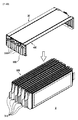
図1は、本開示の多様な実施例と比較するための比較例を説明するための図である。 FIG. 1 is a diagram for explaining comparative examples for comparison with various examples of the present disclosure.
最近、より高い高出力の大容量バッテリーが要求されるに伴い、積層されるバッテリーセルの個数が増加している。この過程で、比較例の軟性回路基板1000は、バッテリーセルのセンシング部が広く形成される形態に裁断されて用いられる。例えば、図1に示すように、バンド状の中心部1110、中心部1110の両端部に形成されて互いに対向するように配置される連結部1120及び連結部から突出してバスバーに第3連結回路部1150を有する形状に裁断される。
Recently, the number of stacked battery cells is increasing with the demand for higher capacity batteries with higher output. In this process, the
前述の比較例において、中心部1110の両側に形成される損失部分aが増加し、軟性回路基板1000の生産歩留まりが多少減少する問題が生じ得る。また、軟性回路基板1000をフレームに組み立てる過程で軟性回路基板が外力などにより破損するか裂けて、軟性回路基板に実装された電気素子が破損するなどの問題が生じ得る。これにより、バッテリーモジュールに加えられる激しい振動や衝撃により軟性回路基板の側面プレートに曲がる部分にクラックが発生する問題が生じ得る。
In the above-mentioned comparative example, there may be a problem that the loss portions a formed on both sides of the
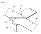
図2は、本開示の一実施例による軟性回路基板100の平面図であり、図3は、図2に示す軟性回路基板100の折る方法を示す図であり、図4は、図2に示す軟性回路基板100の一側の連結部の最終形状を示す斜視図である。図5は、図4に示す重ね合わせ部140を拡大図示した斜視図であり、図6は、図5に示す第1重ね合わせ部141及び第2重ね合わせ部142が接着剤200により固定される方法を示す斜視図である。
FIG. 2 is a plan view of the
図2〜図6を参照すると、バスバーが結合されたフレームに設置されてバッテリーセルの電圧をセンシングするように構成された軟性回路基板100は、バンド状の中心部110、前記中心部110の両端部に形成されて、互いに対向配置される第1連結回路部120、前記第1連結回路部120に折れ曲がって延び前記中心部110と並んで形成される第2連結回路部130を含むことができる。第3連結回路部150は、第1連結回路部120及び第2連結回路部130のそれぞれから延びてバスバーに連結されるように形成され得る。
Referring to FIGS. 2 to 6, the
第2連結回路部130が前記第1連結回路部120の一側に折れる場合、第1連結回路部120と前記第2連結回路部130との間に重ね合わせ部140が形成され得る。重ね合わせ部140が形成される場合、第2連結回路部130は第1連結回路部120と同一線上に配置され得る。
When the second connecting
図9を参考にすると、軟性回路基板100の端面方向への中心には基板層101が形成され、基板層101の上下に絶縁層102がそれぞれ積層されて形成され得る。基板層101は、電気的な信号で情報を伝達する回路として構成され得、絶縁層102は基板層101を保護して他の導電性構成とのショート現象を防止することができる。
With reference to FIG. 9, a
図9を参考にすると、基板層101は、電気伝導性のある金属層で形成され、電気伝導性の高い銅板(copper plate)で形成され得る。絶縁層102は、フィルム(PEN、P1)形態の電気伝導性のない物質で形成され得る。また、基板層101及び絶縁層102のそれぞれは、フレキシブルな特性を有するため、容易に変形され得る。
With reference to FIG. 9, the
再度図2を参考にすると、軟性回路基板100は、中心部110、第1連結回路部120及び第2連結回路部130を含み、第1連結回路部120と前記第2連結回路部130との間に重ね合わせ部140が形成され得る。中心部、第1連結回路部120、第2連結回路部130及び重ね合わせ部140は、軟性回路基板100の部分に該当し得、これらは中心部110とともに1つの軟性回路基板として一体に形成され得る。
With reference to FIG. 2 again, the
中心部110の端部には、第1固定ホール115が形成され得る。また、中心部110及び第2連結回路部130から突出延長した部分に突出ホール112がさらに形成され得る。
A first
中心部110は、バンド状に長く形成され得る。温度センシング部111は、中心部110から外側に延びて形成され得る。温度センシング部111は、一側に複数個が延びて形成されるように提供され得る。温度センシング部111は、バッテリーセルの温度を測定して軟性回路基板100を通じて電気的情報として外部装置に伝達し、過発熱などの現象を検出するように構成され得る。
The
第1連結回路部120と第2連結回路部130は、中心部110の両端部にそれぞれ同一に形成されて適用することができる。以下では、中心部110の一側に形成される部分に基づいて、本開示の多様な実施例について説明する。
The first
第1連結回路部120は、中心部110の両端部にそれぞれ形成される。第1連結回路部120は、中心部110の1つの端部の両側に延長形成され、中心部110に対して垂直の形状を有し得る。また、第1連結回路部120は、中心部110を挟んで互いに対向配置され得る。
The first connecting
第2連結回路部130は、第1連結回路部120から折れ曲がって延びて形成され得る。中心部110が形成された方向に垂直に折れ曲がって中心部110と並んで形成される。第2連結回路部130は、第1連結回路部120の端部にそれぞれ形成され得る。例えば、1つの軟性回路基板100に計4つの第2連結回路部130が形成され得る。
The second connecting
重ね合わせ部140は、第1連結回路部120及び第2連結回路部130の間に形成され得る。重ね合わせ部140は、第2連結回路部130が第1連結回路部120の一側に折れて第2連結回路部130が複数の層で重なる部分と定義され得る。
The superimposing
重ね合わせ部140は、第2連結回路部130が第1ベンディングライン131に沿って第1連結回路部120に向かって上側に折れて形成される第1重ね合わせ部141、及び第2連結回路部130が再度第2ベンディングライン132に沿って第1重ね合わせ部141の第1連結回路部120の長さ方向に上側に折れ曲がって折れて形成される第2重ね合わせ部142を含むことができる。即ち、重ね合わせ部140は、第2連結回路部130が第1ベンディングライン131及び第2ベンディングライン132に沿って折れて形成されるものであって、第2連結回路部130の一部に該当する。
The overlapping
重ね合わせ部140が形成される場合、第2連結回路部130は、第1連結回路部120と平行に配置され得る。また、第2連結回路部130に形成された第3連結回路部150は、第1連結回路部120に形成された第3連結回路部150と平行に配置され得る。本開示の多様な実施例において、両構成が平行に配置される場合、両構成が完全に平行であって延長線が出合わない場合だけでなく、所定の角度に傾いて実質的に平行をなす場合を含む。
When the overlapping
一実施例による軟性回路基板100において、第1ベンディングライン131は、第1連結回路部120の長さ方向と並んで形成され得る。第2ベンディングライン132は、第1ベンディングライン131と約45度の角度で、斜線方向に形成され得る。
In the
図3を参考にして、第2連結回路部130のフォールディング方法について説明する。第2連結回路部130は、中心部110と並んで形成された状態で(第1状態)、第1ベンディングライン131に沿って第1連結回路部120の上側に折れて中心部110の反対側に中心部110と並んで形成された状態となり(第2状態)、第1重ね合わせ部141が第1連結回路部120と第2連結回路部130との間に形成される。次に、第2連結回路部130は、第2ベンディングライン132に沿って第1重ね合わせ部141の上側に折れ曲がって第1連結回路部120と同一線上に配置される状態となり(第3状態)、第1重ね合わせ部141と第2連結回路部130との間には、第2重ね合わせ部142が形成され得る。
A folding method of the second connecting
1つの第2連結回路部130を基準に重ね合わせ部140とベンディングライン131、132は、必ずしも2つに形成されるものではなく、軟性回路基板100の裁断形状及び最終形状に応じて異なる個数で形成され得る。
The overlapping
第1重ね合わせ部141と第2重ね合わせ部142を構成する第2連結回路部130の部分の間は、接着剤200により密着固定され得る。接着剤200は、上側及び下側に同時に固定力を提供するように構成され得る。接着剤200は、例えば、両面テープまたは両面パッドを用いることができる。接着剤200を用いると、軟性回路基板100の重ね合わせに伴う厚さの増大を最小化し、浮き上がりを防止して組み立て過程または車両運行による振動などによる損傷を防止することができる。
The portion of the second connecting
前述の実施例によると、軟性回路基板100は、ベンディング作業が進められる前の裁断された形状と異なる、フォールディング作業が進められた後の最終形状を有し得る。これにより、軟性回路基板100の生産過程における歩留まりを向上させることができ、広い幅を占めるように積層された複数個のバッテリーセルの電圧をそれぞれセンシングできるように構成され得る。
According to the above-described embodiment, the
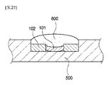
図7は、図4に示す第3連結回路部150の基板層が露出した状態を示す斜視図であり、図8は、図7に示す第1面151及び第2面152を示す平面図であり、図9は、図8に示す第3連結回路部150の断面を示す断面図である。
FIG. 7 is a perspective view showing a state in which the substrate layer of the third connecting
第3連結回路部150は、第1連結回路部120及び第2連結回路部130のそれぞれから分岐されるように、第1連結回路部120及び第2連結回路部130から延びて形成され、一側がバスバーに接合され得る。一実施例による軟性回路基板100において、第1連結回路部120には、複数個の第3連結回路部150が同一方向に延びて形成され得る。また、1つの第3連結回路部150は、第2連結回路部130の端部に延びて形成され得る。
The third
第3連結回路部150は、第2連結回路部130が第1連結回路部120と同一線上に配置される状態(即ち、第3状態)であるとき、第2連結回路部130に形成された第3連結回路部150が第1連結回路部120に形成された第3連結回路部150と同一方向に突出した形態を有するように、同一の方向に並んで配置され得る。
The third
第3連結回路部150は、バスバーに接合されてバッテリーセルのそれぞれの電圧及び電流を測定して電気的な情報として基板層101に沿って伝達することができる。従って、第3連結回路部150の数は、バッテリーセルの個数及びバスバーの個数に応じて、その数が増減されるように調節することができる。
The third
第3連結回路部150の両側面は、軟性回路基板100の内部基板層101が露出するように形成され得、基板層101は、バスバーに接触する第1面151及び第1面151の反対側に形成されて露出する第2面152を含むことができる。
Both side surfaces of the third connecting
第1面151のサイズは、第2面152のサイズより大きく形成され得る。このような構造は、第1面151とバスバーとの接合を容易にすることができ、外部に露出した基板層101の部分を減少させて基板層101の損傷を最小化することができる。
The size of the
他の実施例において、第3連結回路部150は、内部基板層101の一面が露出されるように形成され得る。基板層101の一面の反対側面は絶縁層でカバーされ得る。また、露出した基板層101の一面はバスバーに接触することができる。
In another embodiment, the third
前述の実施例によると、バスバーと第3連結回路部150が直接接合され得るようにして、作業工数を節減させると共に重量及び原価を節減することができる。これについては、バッテリーモジュールの説明時に詳しく述べるようにする。
According to the above-described embodiment, the bus bar and the third connecting
以下、図面を参照して前述の軟性回路基板を含む本開示のバッテリーモジュールの具体的な実施例を詳細に説明する。 Hereinafter, specific examples of the battery module of the present disclosure including the above-mentioned flexible circuit board will be described in detail with reference to the drawings.
[第1実施例] [First Example]
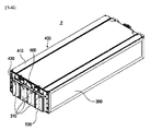
図10は、本開示の第1実施例によるバッテリーモジュール1の斜視図であり、図11は、図10に示すバッテリーモジュール1の分解図であり、図12は、図10に示すバッテリーモジュール1のセル組立体300の斜視図であり、図13は、図10に示すバッテリーモジュール1のフレーム組立体10の斜視図であり、図14は、図13に示すフレーム400の上部プレート410と側面プレート420のヒンジ結合を示す斜視図である。
10 is a perspective view of the
図10〜図14を参照すると、本開示の第1実施例によるバッテリーモジュール1は、1つ以上のバッテリーセルが積層されて形成されるセル組立体300、セル組立体300を固定するためのフレーム組立体10を含むことができる。
Referring to FIGS. 10 to 14, the
フレーム組立体10は、上部プレート410、上部プレート410の両端に連結される側面プレート420を含んで前記セル組立体300を取り囲むように配置されるフレーム400、側面プレート420に配置されて固定されるバスバー500、及び上部プレート410と前記側面プレート420に沿って配置されてバッテリーセルの電圧をセンシングする軟性回路基板100を含むことができる。上部プレート410には、上側面に一定の深さで掘られた経路溝411が形成され得る。
The
セル組立体300は、1つ以上のバッテリーセルが積層されて形成され、バッテリーセルは二次電池で形成されることが一般的であるが、これに限定されるものではなく、充電または放電が可能な電池である場合、いずれででも形成され得る。
The
バッテリーセルは、両側に突出して端子部310が形成され得、一側に(−)端子が形成される場合、他側には(+)端子が形成される。また、導電性物質で形成され、フレキシブルな特性を有して変形可能なものが好ましい。従って、端子部310は、一側に折れて隣接する端子部310と接合工程を通じて電気的に連結される。
The battery cell may project from both sides to form
セル組立体300は、図12に示すように、バッテリーセルが立てられた形態で積層されて形成され得、バッテリーセルは隣接する他のバッテリーセルと端子部310が互いに連結される。例えば、同一極性を有する端子同士連結される場合、バッテリーセルは電気的に並列連結され、互いに異なる極性を有する端子同士連結される場合、バッテリーセルは電気的に直列連結される。
As shown in FIG. 12, the
バッテリーセルの連結は、必要に応じて異ならせて構成することができる。例えば、8つのバッテリーセルを2つずつ並列連結し、並列連結した4つのセルを再度直列連結して4P 3Sとして形成することができる。 The connection of the battery cells can be configured differently as needed. For example, eight battery cells can be connected in parallel by two, and four cells connected in parallel can be connected in series again to form a 4P 3S.
前述の実施例によると、セル組立体300においてバッテリーセルの連結構成を異ならせて車両パッケージに伴うバッテリー容量を容易に変更することができ、接合工程に要される時間を節減して生産性を向上させることができる。
According to the above-described embodiment, in the
図13及び図14を参照すると、フレーム400は、上部プレート410と上部プレート410の両端に連結される側面プレート420を含むことができる。フレーム400の上部プレート410及び側面プレート420は、上部プレート410に形成されたフック部414と側面プレート420に形成されたロッド部424に嵌められてヒンジ結合される。
With reference to FIGS. 13 and 14, the
上部プレート410の端部のそれぞれには、フック状のフック部414が離隔して複数個形成され得、フック部414が形成された位置に対応して側面プレート420の上側面にはロッド部424が形成され得る。フック部414とロッド部424はそれぞれ、上部プレート410及び側面プレート420に突出形成されて、一側で出合うようになり、ロッド部424がフック部414に嵌められてヒンジ結合され得る。
A plurality of hook-shaped
一実施例において、フック部414の内部曲率半径は、ロッド部424の半径と同一か小さく形成され得る。これにより、上部プレート410と側面プレート420の結合において一定以上の固定力が確保され得るため、組み立て過程でフレーム400が分離することを防止して作業性を向上させることができる。
In one embodiment, the internal radius of curvature of the
フレーム400は、上部プレート410がセル組立体300の上側に配置され、側面プレート420は端子部310が形成されたセル組立体300の両側面に配置されて、セル組立体300を取り囲むように配置され得る。
In the
フレーム400は、上部プレート410と側面プレート420がプラスチック射出成形方式で形成され得る。これにより、フレーム400は生産コストが低廉であり、ヒンジ結合されて容易に組み立てられ得る。
In the
図15は、図10に示すバッテリーモジュール1のフレーム400と軟性回路基板100の配置を示す側面図であり、図16は、図13に示すフレーム組立体10の上部プレート410及び軟性回路基板100の結合された構成を示す斜視図であり、図17は、図16に示す上部プレート410及び軟性回路基板100の分解された構成を示す分解斜視図であり、図18は、図17に示す上部プレート410の経路溝411に軟性回路基板100が安着した状態を示す平面図である。
FIG. 15 is a side view showing the arrangement of the
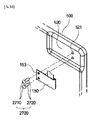
図19は、図10に示すバッテリーモジュール1の側面プレート420の正面図であり、図20は、図19に示す補強プレート600を拡大図示した斜視図であり、図21は、図20に示されたA−A方向の断面斜視図及び断面図であり、図22は、図20に示す補強プレート600の固定方法を示す図であり、図23は、図19に示すバスバー500の安着部520を拡大図示した斜視図である。
19 is a front view of the
軟性回路基板100は、図15に示すように、フレーム400の外側に沿って配置される。中心部110は、上部プレート410の上側面に配置され得る。中心部110は、一定の深さで掘られて形成された経路溝411に安着して固定され、中心部110の長さは、上部プレート410の長さより長く形成されて中心部110の両端部は、側面プレート420に沿って曲がることができる。
The
第1連結回路部120及び第2連結回路部130は側面プレート420の外側に配置され、側面プレート420の外観に沿って曲がって密着する。従って、第1連結回路部120と第2連結回路部130に形成された第3連結回路部150は、構造的にバスバー500の外側に配置され得る。
The first connecting
図2を参考にすると、中心部110及び第2連結回路部130には、突出ホール112が形成され得る。突出ホール112は複数個形成され得、締結部材(図示せず)が貫通して軟性回路基板100をフレーム400に固定させることができる。突出ホール112は、外側に突出するように延長形成され、内部回路には影響を及ぼさない。
With reference to FIG. 2, protruding
軟性回路基板100の一端はバスバー500に電気的に連結され、内部に複数個の線が並んで配列されてバッテリーセルの電圧及び電圧に関する情報をBMS(Battery Management System)(図示せず)側に伝達する。BMSは、各バッテリーセルの充電と放電を管理する。例えば、BMSは充電モードで、互いに異なる電圧レベルに放電された複数個のバッテリーセルを均一な電圧レベルを有するように充電することができる。
One end of the
上部プレート410は、セル組立体300のサイズに対応して四角形状に形成され、セル組立体300の上側に配置される。上側面には、中心部110が安着する経路溝411が形成され、経路溝411の上側を覆うトップカバー413を含む。
The
経路溝411は、中心部110が安着できるように一定の深さで掘られるように形成され得る。トップカバー413は、中心部110が経路溝411に安着した状態で中心部110の上側を覆うことができる。従って、経路溝411とトップカバー413は、中心部110の形状と同一の形状に形成され得る。従って、中心部110はフレーム400の外側に離脱せず、外部に露出しないため、組み立て過程で中心部110に生じ得る損傷が防止され得る。
The
上部プレート410には、経路溝411の内側に向かって突出したリブ412が形成され得る。リブ412は、経路溝411の両側に交互に複数個形成され、互いに一定の間隔を置いて離隔するように形成され得る。
The
リブ412は、経路溝411の両側面から内側に突出するように形成され得、リブ412の下側面は経路溝411から所定の間隔を置いて離隔することができる。従って、中心部110は、リブ412と経路溝411との間に配置されて、中心部110が経路溝411から離脱することを防止するため、両面テープのような接着剤なしでも軟性回路基板100はフレーム400に密着固定され得る。
The
図19を参考にすると、側面プレート420の外側面には、補強プレート600とバスバー500が密着固定され得る。側面プレート420は2つで構成されて、上部プレート410の両端部にそれぞれ連結される。従って、2つの側面プレート420は、セル組立体300の両側面に配置され得る。セル組立体300の両側面は、バッテリーセルの端子部310が形成された両側面となり得る。
With reference to FIG. 19, the reinforcing
補強プレート600は、中心部110の端部を覆って側面プレート420に密着固定され得る。側面プレート420には、補強プレート600の固定のために側面プレート420から突出した融着突起425が形成され得る。中心部110及び補強プレート600のそれぞれには、融着突起425の位置に対応して固定ホール115、615が形成され得る。
The reinforcing
補強プレート600は、融着突起425が中心部110の第1固定ホール115と補強プレート600の第2固定ホール615を順次貫通した後、融着方式で固定され得る。融着突起425は、熱融着工程でヒータが備えられた加圧部材(図示せず)により外側から溶けて圧着され、その後、圧着された部分が冷却されて硬化しつつ、補強プレート600は側面プレート420に密着することができる。
The reinforcing
前述の実施例によると、中心部110の端部は、補強プレート600と側面プレート420との間に配置されて固定され得る。補強プレート600は、中心部110の曲がった部分を通って下側端部部分を加圧するため、加圧により軟性回路基板100が追加で曲がる現象を最小化して、クラックなどのような損傷を防止することができる。また、熱融着工程で軟性回路基板100が直接加圧されることを遮断し、車両の運行による持続的な振動や衝撃などの外力を吸収して損傷を最小化することができる。
According to the above-described embodiment, the end portion of the
ここでの融着工程は、熱融着固定だけでなく、超音波融着固定などを含む。 The fusion step here includes not only heat fusion fixation but also ultrasonic fusion fixation and the like.
補強プレート600は、軟性回路基板100とバスバー500の電気的連結を妨げないように、金属を除く回路のないいかなる絶縁材質でも形成可能である。
The reinforcing
バスバー500は側面プレート420に密着固定されて、一部分は第3連結回路部150と連結され、他の部分は端子部310と連結され得る。従って、バスバー500は、軟性回路基板100とバッテリーセルを電気的に連結するように構成され得る。
The
バスバー500は、互いに離隔するように複数個で提供され得、バスバー500の個数は必要に応じて変更可能である。また、各バスバー500には、挿入ホール510及び安着部520が形成され得る。
A plurality of
安着部520は、各バスバー500の第3連結回路部150と接合される部分となり得、一定の深さで掘られるように形成され得る。従って、作業者は、安着部520に基づいて作業位置を肉眼で識別でき、接合位置を明確に把握することができる。これにより、接合不良などの問題を解決することができる。
The anchoring
挿入ホール510は、バッテリーセルが積層された方向と同一の方向に沿って形成され得る。挿入ホール510にセル組立体300の端子部310が挿入され、挿入ホール510を貫通して突出する端子部310の部分は、一側に折れてバスバー500と接合され得る。従って、バスバー500を介してバッテリーセルは他のバッテリーセルと電気的に連結され得る。
The
このとき、端子部310の挿入のために挿入ホール510が形成された位置に対応して側面プレート420にもホール(図示せず)が形成され得る。
At this time, a hole (not shown) may be formed in the
バスバー500は、それぞれ別途に形成されたセンシングバスバー及びHVバスバーを含むことができる。バスバー500は、セル組立体300の端子部310と電気的に連結されてバッテリーセルのそれぞれの電圧と電流に関する情報を伝達したり、バッテリーモジュール1の外部に設けられたバスバーと連結されて電気的情報を伝達することができる。また、バスバー500は導体で形成され、電気伝導率の高い金属で形成され得る。
The
図24は、図23に示す安着部520に基板層101が直接接合された状態を示す正面図であり、図25は、図24に示す基板層101をバスバー500に接合するための接合方法を示す断面図であり、図26は、図24の第3連結回路部150にコーティング部800がさらに形成された状態を示す平面図であり、図27は、図26に示すコーティング層の断面図である。
FIG. 24 is a front view showing a state in which the
基板層101は、バスバー500に接触する第1面151と第1面151の反対側に形成される第2面152を含み、第2面152の外側にコーティング部800がさらに形成され得る。第1面151と第2面152は、軟性回路基板100の絶縁層102を切削して内部基板層101を露出させることにより形成され得る。
The
第1面151はバスバー500の一側に接触し、第1面151はバスバー500に一定の深さで掘られて形成された安着部520に接触することができる。安着部520は、第3連結回路部150が接合される位置を明確に示して作業性を向上させることができる。
The
一実施例において、第1面151のサイズは、第2面152のサイズより大きく形成され得る。本実施例は、バスバー500との溶接面積を確保することができ、外部に露出する基板層の面積を減少させて第3連結回路部150の損傷を防止することができる。
In one embodiment, the size of the
基板層101は、軟性回路基板100の回路の役割をする構成であって、電気伝導性のある物質で形成され、第1面151と安着部520を直接接合させてバスバー500と軟性回路基板100を電気的に連結させることができる。この過程において、第2面152の外側でレーザ溶接して第1面151を接合させることができる。
The
第1面151は、絶縁層102が切削されて露出した面となり得る。万一、安着部520の外側と絶縁層102の厚さに対応するエアギャップが存在する場合、エアギャップにより接合過程で基板層101が焼ける現象が発生したり、絶縁層102が燃焼する現象が発生したりして、要求される品質を達成することができないこともある。
The
一実施例によると、接合工程において、治具(Z、jig)で第2面152を加圧して第1面151と安着部520との間に存在するエアギャップを除去することができる。また、加圧により安着部520と第1面151の接触面積は増加し、溶接部の固定力を向上させることができる。
According to one embodiment, in the joining step, the
第3連結回路部150は、基板層101の両面に露出するように構成されるため、バスバー500に直接的に結合され得る構造を有することができる。従って、適用部品の減少及び作業工数を節減させてさらに向上した生産性を提供することができる。
Since the third connecting
コーティング部800は、第2面152及び第3連結回路部150の周辺のバスバー500の一部をカバーするように形成され得る。コーティング部800は、基板層101とバスバー500の電気的連結を妨げないように非伝導性材料で構成され得、ノズルを用いて一部にのみ塗布され得る。
The
図27に示すように、コーティング部800は、第1面151がバスバー500に接合された状態で形成され得る。また、第2面152だけでなく、第2面152の周辺絶縁層102及び周辺バスバー500の一部までカバーするように形成されて基板層101の腐食を防止すると共に、バスバー500との接合強度を向上させることができる。
As shown in FIG. 27, the
図28は、図23に示す安着部520に、一実施例による一体型連結端子700の連結部720が接合された状態を示す正面図であり、図29は、図28に示す一実施例による一体型連結端子700の斜視図であり、図30は、図23に示す安着部520に一体型連結端子700と他の実施例であるリング状の連結端子1700の連結部1720が接合された状態を示す正面図であり、図31は、図30に示すリング状の連結端子1700及び締結部材1730の斜視図であり、図32は、図28及び図30に示す固定部710が第3連結回路部150に固定される方法を示す斜視図である。
FIG. 28 is a front view showing a state in which the connecting
軟性回路基板100とバスバー500は、前述の実施例で説明したように、第3連結回路部150に形成された基板層101により電気的に連結可能である。ただし、第3連結回路部150とバスバー500にそれぞれ連結される連結端子700、1700によっても電気的に連結可能である。
As described in the above-described embodiment, the
連結端子700、1700は、固定部710と連結部720、1720を含み、連結部720、1720は、固定部710の一側から延長形成されて一体に形成される。連結端子700、1700は、バスバー500と第3連結回路部150との間に位置し、両側に連結されて第3連結回路部150とバスバー500を電気的に連結するように構成され得る。
The connecting
具体的には、固定部710は、第3連結回路部150に固定される部分であって相対的に狭く形成され、上側及び下側に突出した固定突起711が形成され得る。固定突起711は、互いに離隔するように複数個で提供され、予め設定された位置で整列する第3連結回路部150を貫通することができる。固定突起711の貫通して突出した部分は、撓んで変形されて第3連結回路部150に固定される。
Specifically, the fixing
連結端子700、1700は、様々な実施例を有し得、以下では、互いに異なる実施例に該当する場合であっても同一の部分に対しては同一の符号を用いて説明するようにする。
The connecting
図25に示すように、一実施例による連結端子700の連結部720は、バスバー500の安着部520に接合される部分であって相対的に広く形成され、レーザ溶接により接合され得る。図27に示すように、他の実施例による連結端子1700の連結部1720は、中心にホール1721が形成されたリング状を有し得、リング状は、螺子などのような締結部材1730により固定され得る。
As shown in FIG. 25, the connecting
前述の実施例による連結端子700、1700は、従来は軟性回路基板とバスバーとの連結のために固定端子と連結板を用いたのとは異なり、固定部710と連結部720、1720が一体に連結されて作業の工数を節減し、生産コストを節減させて生産性を向上させることができる。
In the connecting
図33は、図23に示す安着部520に結合部材2700が結合された状態を示す斜視図であり、図34は、図33に示す安着部520に結合部材2700を結合するための結合方法を示す斜視図であり、図35は、図33に示されたB−B方向の断面図である。
FIG. 33 is a perspective view showing a state in which the
軟性回路基板100とバスバー500は、前記のように第3連結回路部150に形成された基板層101または連結端子700、1700により電気的に連結可能である。ただし、結合部材2700は、第3連結回路部150及びバスバー500の間で重ね継ぎされ第3連結回路部150及びバスバー500を電気的に連結することができる。
The
結合部材2700は、第3連結回路部150の外側に配置されるヘッド2710とヘッド2710から延長形成される繋ぎ部2720を含むことができる。繋ぎ部2720は、軟性回路基板とバスバーを電気的に連結することができる。従って、結合部材2700は、電気伝導性を有する金属材質で形成される。ヘッド2710は、繋ぎ部2720から外側に突出して配置され、第3連結回路部150を安着部520側に加圧して第3連結回路150部を安着部520に固定させることができる。
The
結合部材2700との結合のために、安着部520には第1結合ホール521が形成され、第3連結回路部150には、第1結合ホール521の位置に対応して第2結合ホール153が形成され得る。第1結合ホール521及び第2結合ホール153はそれぞれ互いに離隔して一対で形成され、内径が互いに同一に形成され得る。結合部材2700が結合された状態で、繋ぎ部2720は、第2結合ホール153及び第1結合ホール521を順次貫通してバスバー500に固定され得る。また、ヘッド2710は、繋ぎ部2720に外側に延長形成され、第3連結回路部150の外側に突出して配置される。
A
繋ぎ部2720は、第1結合ホール521及び第2結合ホール153と同一のサイズで形成され、ヘッド2710は、繋ぎ部2720の半径よりも大きい半径を有することができる。従って、ヘッド2710は、第1結合ホール521及び第2結合ホール153を貫通することができず、第3連結回路部150の外側に配置され得る。
The connecting
前述の実施例によると、結合部材2700の繋ぎ部2720が第2結合ホール153を貫通し、第3連結回路部150の基板層102と電気的に連結され、再度第1結合ホール521を貫通してバスバー500と電気的に連結されるため、結合部材2700は、軟性回路基板とバスバーを電気的に連結することができる。
According to the above-described embodiment, the connecting
一実施例において、結合部材2700は、永久的な結束力を提供して厚さが薄い部材間で有用に用いられるリベット(rivet)で構成され得る。リベットを用いる場合、溶接工程による歪みや溶接部位に発生する割れ現象などを根本的に防止して結合に対する信頼性を向上させることができる。
In one embodiment, the
[第2実施例] [Second Example]
本開示の第2実施例によるバッテリーモジュール2は、前述の第1実施例によるバッテリーモジュール1と一部の構成が同一であるため、以下では、前述の構成と同一の構成に関する重複説明は省略する。
Since the
図36は、本開示の第2実施例によるバッテリーモジュール2の斜視図であり、図37は、図36に示すフレーム400と軟性回路基板100の分解された構成を示す側面図であり、図38は、図36に示すフレーム400の下側方向における斜視図であり、図39は、図38に示す上部プレート410と軟性回路基板100の分解図である。
36 is a perspective view of the
図36〜図39を参照すると、本開示の第2実施例によるバッテリーモジュール2は、1つ以上のバッテリーセルが積層されて形成されるセル組立体300、及びセル組立体300を固定するためのフレーム組立体20を含むことができる。
With reference to FIGS. 36 to 39 , the
フレーム組立体20は、上部プレート410、前記上部プレート410の両端に連結される側面プレート420を含んで前記セル組立体300を取り囲むように配置されるフレーム400、前記側面プレート420に配置されて固定されるバスバー500、前記上部プレート410と前記側面プレート420に沿って配置されて前記バッテリーセルの電圧をセンシングする軟性回路基板100、前記側面プレート420の一側に密着固定されて前記軟性回路基板100の端部を覆う補強プレート600を含むことができる。前記上部プレート410は、底面に一定の深さで掘られた保護溝416が形成され得る。
The
本開示の第2実施例によるバッテリーモジュール2は、図37に示すように、軟性回路基板100の中心部110は、上部プレート410の底面に配置され得、第1連結回路部120及び第2連結回路部130は、側面プレート420の外側面に配置され得る。
In the
中心部110は、上部プレート410とセル組立体300との間に位置することになり、バッテリーモジュール2の外部に軟性回路基板が露出する部分を最小化することができる。これにより、組み立て過程で生じ得るクラックなどによる裂けなどの軟性回路基板100の損傷を最小化することができる。
The
図39に示すように、フレーム400の上部プレート410は、底面には中心部110が収容される保護溝416が形成され得、保護溝416は、中心部110と同一の形状に形成され得る。
As shown in FIG. 39, the
中心部110は、接着剤200により保護溝416に密着固定され得る。接着剤200は、中心部110及び保護溝416の形状と対応する形状の両面テープ200を用いることができる。両面テープ200により中心部110を固定する場合には、バッテリーモジュール2の組み立て過程で熱融着工程を最小化することができるため、生産時間を短縮させ得、融着工程で加圧により発生する軟性回路基板100の破損を防止することができる。
The
一実施例において、保護溝416が形成された位置に対応して上部プレート410及び側面プレート420のうち、少なくともいずれか1つには保護ホール417が形成され得る。保護ホール417は、中心部110の端部が通過して、第1連結回路部120及び第2連結回路部130が側面プレート420の外側面に配置され得るようにする。
In one embodiment, a
図39を参考にすると、中心部110は、保護ホール417を貫通して曲がりながら浮き上がり部分が生じ得るため、これを最小化するために、保護ホール417は上部プレート410に形成され得る。
With reference to FIG. 39 , the
また、第1連結回路部120及び第2連結回路部130は、中心部110より広く形成されるため、上部プレート410と側面プレート420がヒンジ結合される前に、中心部110が保護溝416に収容されて固定されるようにすることが、フレーム組立体20の組み立てを便利にすることができる。
Further, since the first connecting
以下、本開示のバッテリーモジュール2のセル組立体300とフレーム組立体20が組み立てられる順序について説明する。
Hereinafter, the order in which the
図41は、セル組立体300にフレーム組立体20が組み立てられる方向を示す斜視図であり、図42は、セル組立体300とフレーム組立体20が組み立てられた後に挿入ホール510に端子部310が挿入された状態を示す斜視図であり、図43は、挿入ホール510に端子部310が挿入された後に折れて、バスバー500に連結された状態を示す斜視図であり、図44は、図43に示す端子部310を拡大図示した斜視図である。図45は、バッテリーモジュール2とモノフレーム900の組み立て方法を示す斜視図である。
FIG. 41 is a perspective view showing a direction in which the
一実施例において、1つのバッテリーセルの端子部310は、隣接するバッテリーセルの端子部310と連結されて積層されたセル組立体300を形成することができる。このとき、端子部310は、バッテリーセルの両側に突出した状態で隣接する端子部310と連結され得る。
In one embodiment, the
フレーム400は、上部プレート410と側面プレート420は、ヒンジ結合されて組み立てられた状態となり得る。軟性回路基板100は、フレーム400に沿って配置され得、第3連結回路部150は、バスバー500に接合された状態で配置され得る。
The
図41に示すように、組み立てられたフレーム組立体20は、セル組立体300の上側から下側方向にセル組立体300に結合される。このとき、端子部310が突出しているため、側面プレート420を上部プレート410とのヒンジ結合を中心に外側に回動させて、上部プレート410に対して外側に広がるようにすることができる。従って、フレーム組立体20は、端子部310の妨げなしにセル組立体300の外側を取り囲むように配置され得る。
As shown in FIG. 41, the assembled
次に、図42に示すように、外側に回動させた側面プレート420を再度内側に回動させて元の位置に位置させる。このとき、突出した端子部310は、側面プレート420に形成されたホール(図示せず)及びバスバー500に形成された挿入ホール510を貫通し、端子部310の端部は、バスバー500の外側に突出することができる。
Next, as shown in FIG. 42, the
端子部310の端部は、バッテリーセルと隣接するバッテリーセルの端子部310が接合されたものであって、複数の端子部310が付着して形成されたものである。
The end portion of the
次に、図43に示すように、外側に突出して形成された端子部310の端部は一側に折れてバスバー500の外側面に接合される。接合された状態を見ると、図44に示すように、端子部310の端部は隣接する他の端子部310の端部と接触しないため、1つの端子部310と他の端子部310の接合で連結されたバッテリーセルは、バスバー500によってのみ他のバッテリーセルと電気的に連結され得る。
Next, as shown in FIG. 43, the end portion of the
一実施例において、端子部310とバスバー500は、結合のための別途の構成を提供しなくても、端子部310の端部の外側でレーザ溶接で接合され、バッテリーモジュールの生産に要される時間及びコストを節減することができる。
In one embodiment, the terminal 310 and the
図45を参考にすると、前記のような方法により、組み立てられたバッテリーモジュール2は、モノフレーム900ともう一度組み立てられて固定され得る。モノフレーム900は、車両の事故発生時に、セル組立体300の潰れまたは破損を防止して、これによる火災などの2次的事故の発生を予防する。また、外部衝撃からフレーム400及びセル組立体300の結合状態を保護する。また、モノフレーム900は、高強度を有する金属材料などで形成され得る。
With reference to FIG. 45, the assembled
以上、一部の実施例と添付の図面に示す例により本開示の技術的思想が説明されたものの、本開示が属する技術分野で通常の知識を有する者が理解できる本開示の技術的思想及び範囲を逸脱しない範囲で多様な置換、変形及び変更がなされ得るという点を知らなければならない。また、そのような置換、変形及び変更は、添付の請求の範囲内に属するものと考えられるべきである。 Although the technical idea of the present disclosure has been explained by some examples and the examples shown in the attached drawings, the technical idea of the present disclosure and the technical idea of the present disclosure that can be understood by a person having ordinary knowledge in the technical field to which the present disclosure belongs. It must be known that various substitutions, modifications and changes can be made without departing from the range. Also, such substitutions, modifications and alterations should be considered to be within the scope of the appended claims.
Claims (31)
Applications Claiming Priority (19)
| Application Number | Priority Date | Filing Date | Title |
|---|---|---|---|
| KR1020160180293A KR101928073B1 (en) | 2016-12-27 | 2016-12-27 | Connecting structure of bus-bar assembly |
| KR10-2016-0180292 | 2016-12-27 | ||
| KR10-2016-0180293 | 2016-12-27 | ||
| KR1020160180292A KR101928065B1 (en) | 2016-12-27 | 2016-12-27 | Connecting structure of bus-bar assembly |
| KR1020160182296A KR101928066B1 (en) | 2016-12-29 | 2016-12-29 | Connecting structure of bus-bar assembly |
| KR10-2016-0182296 | 2016-12-29 | ||
| KR1020160183890A KR101844852B1 (en) | 2016-12-30 | 2016-12-30 | Fpcb fixing structure of battery cell module |
| KR10-2016-0183890 | 2016-12-30 | ||
| KR20170026828 | 2017-02-28 | ||
| KR10-2017-0026828 | 2017-02-28 | ||
| KR10-2017-0113677 | 2017-09-06 | ||
| KR1020170113677A KR101996449B1 (en) | 2017-09-06 | 2017-09-06 | Battery cell module with protective structure of fpcb |
| KR1020170141527A KR102033001B1 (en) | 2017-02-28 | 2017-10-27 | Frame assembly, method of manufacturing frame assembly, and method of manufacturing battery module |
| KR10-2017-0141526 | 2017-10-27 | ||
| KR10-2017-0141527 | 2017-10-27 | ||
| KR1020170141526A KR102032999B1 (en) | 2017-02-28 | 2017-10-27 | Battery frame assembly and method for manufacturing same |
| KR1020170159696A KR102087699B1 (en) | 2017-11-27 | 2017-11-27 | Flexible circuit board and battery pack having the same |
| KR10-2017-0159696 | 2017-11-27 | ||
| PCT/KR2017/015594 WO2018124751A1 (en) | 2016-12-27 | 2017-12-27 | Flexible circuit board and frame assembly including same |
Publications (2)
| Publication Number | Publication Date |
|---|---|
| JP2020514976A JP2020514976A (en) | 2020-05-21 |
| JP6869355B2 true JP6869355B2 (en) | 2021-05-12 |
Family
ID=67483407
Family Applications (1)
| Application Number | Title | Priority Date | Filing Date |
|---|---|---|---|
| JP2019536176A Active JP6869355B2 (en) | 2016-12-27 | 2017-12-27 | Flexible circuit board and frame assembly containing it |
Country Status (7)
| Country | Link |
|---|---|
| US (1) | US11309593B2 (en) |
| EP (1) | EP3565022B1 (en) |
| JP (1) | JP6869355B2 (en) |
| CN (1) | CN110114905B (en) |
| HU (1) | HUE054599T2 (en) |
| PL (1) | PL3565022T3 (en) |
| RS (1) | RS61814B1 (en) |
Families Citing this family (23)
| Publication number | Priority date | Publication date | Assignee | Title |
|---|---|---|---|---|
| EP3804947A1 (en) * | 2017-04-04 | 2021-04-14 | Dae San Electronics Co., Ltd. | Bus bar manufacturing method and bus bar manufactured thereby |
| KR102340898B1 (en) | 2018-03-30 | 2021-12-16 | 주식회사 엘지에너지솔루션 | Battery module having a bus bar frame with improved assembly |
| JP6940452B2 (en) * | 2018-04-18 | 2021-09-29 | 株式会社オートネットワーク技術研究所 | Wiring module |
| KR102354401B1 (en) | 2018-04-25 | 2022-01-20 | 주식회사 엘지에너지솔루션 | Battery module and battery pack including the same |
| JP7081355B2 (en) * | 2018-07-13 | 2022-06-07 | 株式会社デンソー | Monitoring device |
| KR20200012189A (en) * | 2018-07-26 | 2020-02-05 | 주식회사 엘지화학 | Busbar assembly |
| KR102349918B1 (en) | 2018-11-21 | 2022-01-10 | 주식회사 엘지에너지솔루션 | Battery module |
| KR102317638B1 (en) | 2018-12-05 | 2021-10-25 | 주식회사 엘지에너지솔루션 | Battery module having protection structure of cell stack |
| KR102371373B1 (en) | 2018-12-06 | 2022-03-04 | 주식회사 엘지에너지솔루션 | Battery module |
| KR102317639B1 (en) | 2018-12-07 | 2021-10-25 | 주식회사 엘지에너지솔루션 | Battery module including insert injection molded busbar |
| KR102395683B1 (en) * | 2018-12-26 | 2022-05-06 | 주식회사 엘지에너지솔루션 | A battery module having a connector mounted on an FPCB, a battery pack and a vehicle comprising the same |
| KR102381762B1 (en) | 2019-02-21 | 2022-03-31 | 주식회사 엘지에너지솔루션 | Battery module including protection cover covering flexible printed circuit board |
| JP7016836B2 (en) * | 2019-06-10 | 2022-02-07 | 矢崎総業株式会社 | Conductive system |
| CN210467965U (en) * | 2019-09-23 | 2020-05-05 | 宁德时代新能源科技股份有限公司 | Battery module, battery pack and vehicle |
| CN112582690A (en) * | 2019-09-29 | 2021-03-30 | 比亚迪股份有限公司 | Flexible circuit board, die-cut substrate, and battery device |
| KR20210051723A (en) * | 2019-10-31 | 2021-05-10 | 에스케이이노베이션 주식회사 | Sensing assembly and battery module comprising the same |
| CN110993410A (en) * | 2019-12-20 | 2020-04-10 | 惠州Tcl移动通信有限公司 | Key module and terminal |
| JP7177109B2 (en) * | 2020-03-02 | 2022-11-22 | 矢崎総業株式会社 | conductive module |
| KR20210156089A (en) * | 2020-06-17 | 2021-12-24 | 주식회사 엘지에너지솔루션 | Battery module with non-welded structure as a connection structure between a busbar and a voltage sensing member |
| KR102485174B1 (en) * | 2020-08-26 | 2023-01-04 | 한화솔루션 주식회사 | Manufacturing method of busbar assembly of battery module for easy filling of high stepped parts |
| CN113422151B (en) * | 2021-06-09 | 2023-02-28 | 东莞新能德科技有限公司 | Method for manufacturing battery, battery and electric equipment |
| JP7421588B2 (en) | 2022-03-25 | 2024-01-24 | 本田技研工業株式会社 | battery pack |
| CN116706447B (en) * | 2023-08-04 | 2023-11-24 | 广州凯风新能源科技有限公司 | Atomizing power supply structure and production process thereof |
Family Cites Families (48)
| Publication number | Priority date | Publication date | Assignee | Title |
|---|---|---|---|---|
| JP3680720B2 (en) * | 2000-08-31 | 2005-08-10 | 住友電装株式会社 | Assembly method of electrical junction box |
| JP2002165338A (en) * | 2000-11-22 | 2002-06-07 | Yazaki Corp | Cabling method for circuit body in electric connection box and cabling structure for circuit body using the cabling method |
| JP2003204619A (en) * | 2001-10-24 | 2003-07-18 | Fujikura Ltd | Electric junction box and connector |
| US7889139B2 (en) * | 2007-06-21 | 2011-02-15 | Apple Inc. | Handheld electronic device with cable grounding |
| KR100933864B1 (en) | 2008-03-31 | 2009-12-24 | 삼성에스디아이 주식회사 | Battery pack |
| WO2010113455A1 (en) * | 2009-03-31 | 2010-10-07 | 三洋電機株式会社 | Battery module, battery system, and electric vehicle |
| KR101023921B1 (en) | 2009-04-01 | 2011-03-22 | 주식회사 엘지화학 | Voltage detection member and battery module including same |
| KR101106404B1 (en) | 2009-11-24 | 2012-01-17 | 삼성에스디아이 주식회사 | Secondary battery and method of making the same |
| KR101328826B1 (en) | 2009-11-24 | 2013-11-13 | 엘지디스플레이 주식회사 | Liquid crystal display and method of local dimming thereof |
| KR20120005728A (en) | 2010-07-09 | 2012-01-17 | (주)브이이엔에스 | A sub pack module |
| JP2011210710A (en) | 2010-03-12 | 2011-10-20 | Autonetworks Technologies Ltd | Battery module |
| JP2011210711A (en) | 2010-03-12 | 2011-10-20 | Autonetworks Technologies Ltd | Battery module |
| US20110255250A1 (en) * | 2010-04-19 | 2011-10-20 | Richard Hung Minh Dinh | Printed circuit board components for electronic devices |
| JP5715766B2 (en) | 2010-04-22 | 2015-05-13 | 矢崎総業株式会社 | Wiring material connection structure |
| US8609266B2 (en) | 2011-02-18 | 2013-12-17 | Samsung Sdi Co., Ltd. | Battery pack |
| KR101273339B1 (en) | 2011-03-24 | 2013-06-11 | 주식회사 이랜텍 | Battery cell of lamination type |
| JP2012227004A (en) | 2011-04-20 | 2012-11-15 | Auto Network Gijutsu Kenkyusho:Kk | Battery connection assembly and battery module |
| KR101866369B1 (en) | 2011-07-12 | 2018-06-14 | 에스케이이노베이션 주식회사 | Battery case |
| KR101853397B1 (en) | 2011-09-01 | 2018-04-30 | 엘지전자 주식회사 | Battery Module |
| JP2013097894A (en) * | 2011-10-28 | 2013-05-20 | Auto Network Gijutsu Kenkyusho:Kk | Battery wiring module |
| JP2013098032A (en) | 2011-11-01 | 2013-05-20 | Auto Network Gijutsu Kenkyusho:Kk | Connection structure of voltage detection terminal |
| US20130149586A1 (en) | 2011-12-09 | 2013-06-13 | Samsung Sdi Co., Ltd. | Battery cell |
| PT2608338E (en) * | 2011-12-21 | 2014-02-21 | 3M Innovative Properties Co | Terminal connection device for a power cable |
| KR101329250B1 (en) | 2012-07-06 | 2013-11-13 | 한국단자공업 주식회사 | Cell busbar fastening structure for series connection apparatus of battery module |
| KR101329252B1 (en) | 2012-07-11 | 2013-11-13 | 한국단자공업 주식회사 | Series connection apparatus of battery module |
| KR101329251B1 (en) | 2012-07-11 | 2013-11-13 | 한국단자공업 주식회사 | Series connection apparatus of battery module |
| US20140193680A1 (en) | 2013-01-08 | 2014-07-10 | Samsung Sdi Co., Ltd. | Battery module |
| KR20140095660A (en) | 2013-01-24 | 2014-08-04 | 엘지전자 주식회사 | Battery Cell Case And Battery Pack Comprising The Same |
| JP6119385B2 (en) * | 2013-04-03 | 2017-04-26 | 株式会社Gsユアサ | Battery module |
| US20140329124A1 (en) | 2013-05-02 | 2014-11-06 | Arcimoto, Llc | Battery pack design for integrating and monitoring multiple single battery cells |
| KR102046122B1 (en) | 2013-05-21 | 2019-11-19 | 에스케이이노베이션 주식회사 | PCB connecting unit for Battery modularizaton and Method for manufacturing Battery module and Battery module made by the method |
| KR20140139862A (en) | 2013-05-28 | 2014-12-08 | 삼성에스디아이 주식회사 | Battery pack |
| KR101490026B1 (en) | 2013-05-31 | 2015-02-06 | 박용미 | Battery Pack And Production Method For The Same |
| US20140370355A1 (en) | 2013-06-14 | 2014-12-18 | Samsung Sdi Co., Ltd. | Battery pack |
| KR20150033176A (en) | 2013-09-23 | 2015-04-01 | 주식회사 엘지화학 | Battery module and busbar applied for the same |
| KR102258973B1 (en) | 2013-10-31 | 2021-06-02 | 타이코에이엠피 주식회사 | A sensing block and a battery package comprising thereof |
| KR20150067694A (en) | 2013-12-10 | 2015-06-18 | 한국단자공업 주식회사 | Connecting apparatus for battery Module |
| JP2015118731A (en) | 2013-12-16 | 2015-06-25 | 日立金属株式会社 | Wire material, secondary battery device, electronic apparatus, and producing method of wire material |
| KR101723037B1 (en) | 2014-08-08 | 2017-04-06 | 주식회사 유라코퍼레이션 | Apparatus for connecting secondary cells in battery pack |
| KR20160026469A (en) | 2014-09-01 | 2016-03-09 | 에스케이이노베이션 주식회사 | battery module having bus bar integrated with low-voltage sensing module |
| KR102142661B1 (en) | 2014-10-07 | 2020-09-14 | 현대자동차주식회사 | Battery Cell Module |
| KR20160044654A (en) | 2014-10-15 | 2016-04-26 | 세방전지(주) | Sensing board for battery pack module |
| KR102258286B1 (en) | 2014-10-21 | 2021-05-31 | 에스케이이노베이션 주식회사 | Battery cell, and battery module |
| KR101750489B1 (en) | 2014-11-24 | 2017-06-23 | 주식회사 엘지화학 | Temperature Sensor for Battery Module and Battery Module Having the Same |
| KR101647694B1 (en) | 2014-12-15 | 2016-08-23 | 현대오트론 주식회사 | Apparatus for measuring voltage and method thereof |
| KR101865995B1 (en) | 2015-03-27 | 2018-06-08 | 주식회사 엘지화학 | Battery module |
| KR20170001135U (en) | 2015-09-18 | 2017-03-28 | 동우 화인켐 주식회사 | Bonding device of FPCB |
| KR102511737B1 (en) * | 2018-01-24 | 2023-03-20 | 삼성전자주식회사 | Antenna structure and electronic device comprising antenna structure |
-
2017
- 2017-12-27 EP EP17888917.6A patent/EP3565022B1/en active Active
- 2017-12-27 PL PL17888917T patent/PL3565022T3/en unknown
- 2017-12-27 US US16/474,414 patent/US11309593B2/en active Active
- 2017-12-27 CN CN201780081162.4A patent/CN110114905B/en active Active
- 2017-12-27 JP JP2019536176A patent/JP6869355B2/en active Active
- 2017-12-27 HU HUE17888917A patent/HUE054599T2/en unknown
- 2017-12-27 RS RS20210557A patent/RS61814B1/en unknown
Also Published As
| Publication number | Publication date |
|---|---|
| HUE054599T2 (en) | 2021-09-28 |
| US20190348720A1 (en) | 2019-11-14 |
| CN110114905B (en) | 2022-06-24 |
| CN110114905A (en) | 2019-08-09 |
| EP3565022A4 (en) | 2020-03-11 |
| PL3565022T3 (en) | 2021-10-04 |
| EP3565022B1 (en) | 2021-03-10 |
| RS61814B1 (en) | 2021-06-30 |
| EP3565022A1 (en) | 2019-11-06 |
| US11309593B2 (en) | 2022-04-19 |
| JP2020514976A (en) | 2020-05-21 |
Similar Documents
| Publication | Publication Date | Title |
|---|---|---|
| JP6869355B2 (en) | Flexible circuit board and frame assembly containing it | |
| KR102087699B1 (en) | Flexible circuit board and battery pack having the same | |
| JP6905071B2 (en) | Frame assembly and method for manufacturing it | |
| JP6757856B2 (en) | Busbar assembly and frame assembly | |
| EP1992026B1 (en) | Battery module | |
| CN101395737B (en) | Middle or large-sized battery module | |
| CN101490871B (en) | Middle or large-sized battery module | |
| JP7045568B2 (en) | Battery module including sensing assembly and busbar assembly | |
| US8691409B2 (en) | Battery module having sensing member with novel structure | |
| KR101264550B1 (en) | Battery Pack | |
| JP5420058B2 (en) | Medium or large battery modules with improved safety | |
| CN102414904A (en) | Voltage sensing member and battery module comprising same | |
| EP3101714B1 (en) | Battery module having voltage sensing member having receptacle structure | |
| US9372237B2 (en) | Battery pack having stable measuring unit | |
| KR20170032098A (en) | Battery module and protecting structure applied for the same | |
| CN112821002B (en) | Battery module and vehicle with same | |
| KR20190106161A (en) | Battery Pack using battery module with short-circuit protection structure |
Legal Events
| Date | Code | Title | Description |
|---|---|---|---|
| A521 | Request for written amendment filed |
Free format text: JAPANESE INTERMEDIATE CODE: A523 Effective date: 20190814 |
|
| A621 | Written request for application examination |
Free format text: JAPANESE INTERMEDIATE CODE: A621 Effective date: 20190703 |
|
| A131 | Notification of reasons for refusal |
Free format text: JAPANESE INTERMEDIATE CODE: A131 Effective date: 20200818 |
|
| A521 | Request for written amendment filed |
Free format text: JAPANESE INTERMEDIATE CODE: A523 Effective date: 20201029 |
|
| TRDD | Decision of grant or rejection written | ||
| A01 | Written decision to grant a patent or to grant a registration (utility model) |
Free format text: JAPANESE INTERMEDIATE CODE: A01 Effective date: 20210323 |
|
| A61 | First payment of annual fees (during grant procedure) |
Free format text: JAPANESE INTERMEDIATE CODE: A61 Effective date: 20210413 |
|
| R150 | Certificate of patent or registration of utility model |
Ref document number: 6869355 Country of ref document: JP Free format text: JAPANESE INTERMEDIATE CODE: R150 |