JP6861463B2 - 露光装置及び物品の製造方法 - Google Patents
露光装置及び物品の製造方法 Download PDFInfo
- Publication number
- JP6861463B2 JP6861463B2 JP2015121423A JP2015121423A JP6861463B2 JP 6861463 B2 JP6861463 B2 JP 6861463B2 JP 2015121423 A JP2015121423 A JP 2015121423A JP 2015121423 A JP2015121423 A JP 2015121423A JP 6861463 B2 JP6861463 B2 JP 6861463B2
- Authority
- JP
- Japan
- Prior art keywords
- substrate
- illuminance
- exposure
- light
- rotation speed
- Prior art date
- Legal status (The legal status is an assumption and is not a legal conclusion. Google has not performed a legal analysis and makes no representation as to the accuracy of the status listed.)
- Active
Links
Images


Classifications
-
- G—PHYSICS
- G03—PHOTOGRAPHY; CINEMATOGRAPHY; ANALOGOUS TECHNIQUES USING WAVES OTHER THAN OPTICAL WAVES; ELECTROGRAPHY; HOLOGRAPHY
- G03F—PHOTOMECHANICAL PRODUCTION OF TEXTURED OR PATTERNED SURFACES, e.g. FOR PRINTING, FOR PROCESSING OF SEMICONDUCTOR DEVICES; MATERIALS THEREFOR; ORIGINALS THEREFOR; APPARATUS SPECIALLY ADAPTED THEREFOR
- G03F7/00—Photomechanical, e.g. photolithographic, production of textured or patterned surfaces, e.g. printing surfaces; Materials therefor, e.g. comprising photoresists; Apparatus specially adapted therefor
- G03F7/20—Exposure; Apparatus therefor
- G03F7/2002—Exposure; Apparatus therefor with visible light or UV light, through an original having an opaque pattern on a transparent support, e.g. film printing, projection printing; by reflection of visible or UV light from an original such as a printed image
- G03F7/201—Exposure; Apparatus therefor with visible light or UV light, through an original having an opaque pattern on a transparent support, e.g. film printing, projection printing; by reflection of visible or UV light from an original such as a printed image characterised by an oblique exposure; characterised by the use of plural sources; characterised by the rotation of the optical device; characterised by a relative movement of the optical device, the light source, the sensitive system or the mask
-
- G—PHYSICS
- G03—PHOTOGRAPHY; CINEMATOGRAPHY; ANALOGOUS TECHNIQUES USING WAVES OTHER THAN OPTICAL WAVES; ELECTROGRAPHY; HOLOGRAPHY
- G03F—PHOTOMECHANICAL PRODUCTION OF TEXTURED OR PATTERNED SURFACES, e.g. FOR PRINTING, FOR PROCESSING OF SEMICONDUCTOR DEVICES; MATERIALS THEREFOR; ORIGINALS THEREFOR; APPARATUS SPECIALLY ADAPTED THEREFOR
- G03F7/00—Photomechanical, e.g. photolithographic, production of textured or patterned surfaces, e.g. printing surfaces; Materials therefor, e.g. comprising photoresists; Apparatus specially adapted therefor
- G03F7/70—Microphotolithographic exposure; Apparatus therefor
- G03F7/70483—Information management; Active and passive control; Testing; Wafer monitoring, e.g. pattern monitoring
- G03F7/7055—Exposure light control in all parts of the microlithographic apparatus, e.g. pulse length control or light interruption
- G03F7/70558—Dose control, i.e. achievement of a desired dose
-
- G—PHYSICS
- G03—PHOTOGRAPHY; CINEMATOGRAPHY; ANALOGOUS TECHNIQUES USING WAVES OTHER THAN OPTICAL WAVES; ELECTROGRAPHY; HOLOGRAPHY
- G03F—PHOTOMECHANICAL PRODUCTION OF TEXTURED OR PATTERNED SURFACES, e.g. FOR PRINTING, FOR PROCESSING OF SEMICONDUCTOR DEVICES; MATERIALS THEREFOR; ORIGINALS THEREFOR; APPARATUS SPECIALLY ADAPTED THEREFOR
- G03F7/00—Photomechanical, e.g. photolithographic, production of textured or patterned surfaces, e.g. printing surfaces; Materials therefor, e.g. comprising photoresists; Apparatus specially adapted therefor
- G03F7/20—Exposure; Apparatus therefor
- G03F7/2002—Exposure; Apparatus therefor with visible light or UV light, through an original having an opaque pattern on a transparent support, e.g. film printing, projection printing; by reflection of visible or UV light from an original such as a printed image
- G03F7/2004—Exposure; Apparatus therefor with visible light or UV light, through an original having an opaque pattern on a transparent support, e.g. film printing, projection printing; by reflection of visible or UV light from an original such as a printed image characterised by the use of a particular light source, e.g. fluorescent lamps or deep UV light
-
- G—PHYSICS
- G03—PHOTOGRAPHY; CINEMATOGRAPHY; ANALOGOUS TECHNIQUES USING WAVES OTHER THAN OPTICAL WAVES; ELECTROGRAPHY; HOLOGRAPHY
- G03F—PHOTOMECHANICAL PRODUCTION OF TEXTURED OR PATTERNED SURFACES, e.g. FOR PRINTING, FOR PROCESSING OF SEMICONDUCTOR DEVICES; MATERIALS THEREFOR; ORIGINALS THEREFOR; APPARATUS SPECIALLY ADAPTED THEREFOR
- G03F7/00—Photomechanical, e.g. photolithographic, production of textured or patterned surfaces, e.g. printing surfaces; Materials therefor, e.g. comprising photoresists; Apparatus specially adapted therefor
- G03F7/70—Microphotolithographic exposure; Apparatus therefor
- G03F7/70008—Production of exposure light, i.e. light sources
-
- G—PHYSICS
- G03—PHOTOGRAPHY; CINEMATOGRAPHY; ANALOGOUS TECHNIQUES USING WAVES OTHER THAN OPTICAL WAVES; ELECTROGRAPHY; HOLOGRAPHY
- G03F—PHOTOMECHANICAL PRODUCTION OF TEXTURED OR PATTERNED SURFACES, e.g. FOR PRINTING, FOR PROCESSING OF SEMICONDUCTOR DEVICES; MATERIALS THEREFOR; ORIGINALS THEREFOR; APPARATUS SPECIALLY ADAPTED THEREFOR
- G03F7/00—Photomechanical, e.g. photolithographic, production of textured or patterned surfaces, e.g. printing surfaces; Materials therefor, e.g. comprising photoresists; Apparatus specially adapted therefor
- G03F7/70—Microphotolithographic exposure; Apparatus therefor
- G03F7/70216—Mask projection systems
- G03F7/70258—Projection system adjustments, e.g. adjustments during exposure or alignment during assembly of projection system
- G03F7/70266—Adaptive optics, e.g. deformable optical elements for wavefront control, e.g. for aberration adjustment or correction
-
- G—PHYSICS
- G03—PHOTOGRAPHY; CINEMATOGRAPHY; ANALOGOUS TECHNIQUES USING WAVES OTHER THAN OPTICAL WAVES; ELECTROGRAPHY; HOLOGRAPHY
- G03F—PHOTOMECHANICAL PRODUCTION OF TEXTURED OR PATTERNED SURFACES, e.g. FOR PRINTING, FOR PROCESSING OF SEMICONDUCTOR DEVICES; MATERIALS THEREFOR; ORIGINALS THEREFOR; APPARATUS SPECIALLY ADAPTED THEREFOR
- G03F7/00—Photomechanical, e.g. photolithographic, production of textured or patterned surfaces, e.g. printing surfaces; Materials therefor, e.g. comprising photoresists; Apparatus specially adapted therefor
- G03F7/70—Microphotolithographic exposure; Apparatus therefor
- G03F7/70691—Handling of masks or workpieces
- G03F7/70758—Drive means, e.g. actuators, motors for long- or short-stroke modules or fine or coarse driving
Landscapes
- Physics & Mathematics (AREA)
- General Physics & Mathematics (AREA)
- Optics & Photonics (AREA)
- Exposure And Positioning Against Photoresist Photosensitive Materials (AREA)
- Exposure Of Semiconductors, Excluding Electron Or Ion Beam Exposure (AREA)
Description
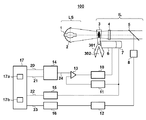
図1は、本発明の一側面としての露光装置100の構成を示す概略図である。露光装置100は、物品としての半導体素子、液晶表示素子、薄膜磁気ヘッドなどのデバイスの製造に用いられ、基板を露光するリソグラフィ装置である。露光装置100は、本実施形態では、ステッパ方式でレチクル(マスク)のパターンを基板に転写する。
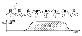
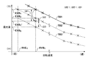
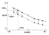
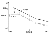
紫外線ランプ1を交換した際には、回転シャッタ3の回転速度に対して基準となる基板の露光量の関係性、即ち、回転シャッタ3の回転速度と、連続駆動モードで回転シャッタ3を回転させたときの基板の露光量との関係を取得する。図3は、回転シャッタ3の回転速度と基板の露光量との関係の一例を示す図である。
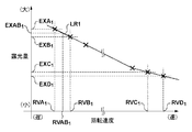
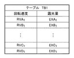
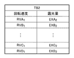
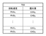
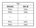
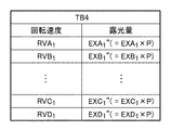
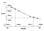
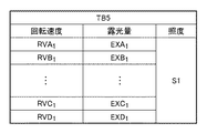
本実施形態では、回転シャッタ3の回転速度と基板の露光量との関係を示す可変テーブルTB4をメモリ17bに記憶させ、光源部LSからの光の照度の変化に応じて、メモリ17bに記憶された可変テーブルTB4における関係を更新する。図9は、回転シャッタ3の回転速度に対して基準となる基板の露光量の関係性、即ち、回転シャッタ3の回転速度と、連続駆動モードで回転シャッタ3を回転させたときの基板の露光量との関係の一例を示す図である。図10は、図9に示す回転シャッタ3の回転速度と基板の露光量との関係をテーブル化して得られる可変テーブルTB4の一例を示す図である。
第1の実施形態及び第2の実施形態では、回転シャッタ3の回転速度と基板の露光量との関係を示すテーブルを更新する際に、光源部LSからの光の照度の変化に関する第2情報として、基板の露光量の経時変化を用いている。但し、光源部LSからの光の照度の変化に関する第2情報として、光源部LSからの光の照度の経時変化を用いてもよい。
第3の実施形態では、ディテクタ8によって検出された光源部LSからの光の照度に基づいて、メモリ17bに記憶された可変テーブルを更新する場合について説明した。但し、紫外線ランプ1を含む光源部LSからの光の照度は、一般的に、その使用時間に応じて低下する傾向がある。
本発明の実施形態における物品の製造方法は、例えば、デバイス(半導体デバイス、磁気記憶媒体、液晶表示素子など)などの物品を製造するのに好適である。かかる製造方法は、露光装置100を用いて、感光剤が塗布された基板を露光する工程と、露光された基板を現像する工程を含む。また、かかる製造方法は、他の周知の工程(酸化、成膜、蒸着、ドーピング、平坦化、エッチング、レジスト剥離、ダイシング、ボンディング、パッケージングなど)を含みうる。本実施形態における物品の製造方法は、従来に比べて、物品の性能、品質、生産性及び生産コストの少なくとも1つにおいて有利である。
Claims (10)
- 光源からの光により基板を露光する露光装置であって、
前記光を遮光する遮光部を含み、前記基板への前記光の入射を制御するための回転シャッタと、
前記回転シャッタの回転速度と、当該回転速度で、前記回転シャッタの回転を停止させずに、前記回転シャッタが前記光を遮光する第1状態から前記回転シャッタが前記光を通過させる第2状態への移行、前記第2状態における前記基板の露光、前記第2状態から前記第1状態への移行の順に行うように、前記回転シャッタを回転させたときの前記基板の露光量との関係を示す第1情報に基づいて、前記基板のショット領域に対する露光処理における前記基板の露光量が目標露光量となるように、前記回転シャッタの回転速度を制御する制御部と、を有し、
前記制御部は、前記光の照度が第1照度から第2照度に低下する場合に、前記第1照度から前記第2照度への変化に関する第2情報に基づいて、前記第1情報に含まれる、前記第1照度に対する前記関係を示す第1テーブル又は第1関数を、前記第2照度に対する前記関係を示す第2テーブル又は第2関数になるように、前記第1情報の更新を行い、更新された前記第1情報に基づき前記回転速度を制御することを特徴とする露光装置。 - 前記関係が互いに異なる複数の第1情報を記憶する記憶部を更に有し、
前記制御部は、前記第2情報に基づいて、前記記憶部に記憶された複数の第1情報から1つの第1情報を選択することで前記更新を行うことを特徴とする請求項1に記載の露光装置。 - 前記基板の露光量を計測する計測部を更に有し、
前記制御部は、前記ショット領域に対する露光処理における前記回転シャッタの回転速度を決定する前に前記回転シャッタを第1回転速度で回転させながら前記計測部によって計測された第1露光量と、前記第1回転速度とに基づいて、前記複数の第1情報から前記1つの第1情報を選択することを特徴とする請求項2に記載の露光装置。 - 前記制御部は、前記複数の第1情報のうち、前記第1回転速度と前記第1露光量との関係に最も近い関係を含む第1情報を前記1つの第1情報として選択することを特徴とする請求項3に記載の露光装置。
- 前記基板の露光量を計測する計測部を更に有し、
前記制御部は、前記ショット領域に対する露光処理における前記回転シャッタの回転速度を決定する前に前記回転シャッタを第1回転速度で回転させながら前記計測部によって計測された露光量と、前記第1情報における前記第1回転速度に対応する前記基板の露光量との変化率を、前記関係に反映させることで前記更新を行うことを特徴とする請求項1に記載の露光装置。 - 前記光の照度を検出する検出部を更に有し、
前記制御部は、前記ショット領域に対する露光処理における前記回転シャッタの回転速度を決定する前に前記検出部によって前記光の照度を検出させることにより前記第1照度及び前記第2照度を求め、前記第2照度と、前記第1照度との変化率を、前記関係に反映させることで前記更新を行うことを特徴とする請求項1に記載の露光装置。 - 前記制御部は、
前記光の初期照度と、前記光源の使用時間とに基づいて、前記第1照度及び前記第2照度を求め、
前記第2照度と、前記第1照度との変化率を、前記関係に反映させることで前記更新を行うことを特徴とする請求項1に記載の露光装置。 - 前記第2情報は、前記光の照度の積分量の経時変化及び前記光の照度の経時変化の少なくとも一方を含むことを特徴とする請求項1乃至7のうちいずれか1項に記載の露光装置。
- 前記制御部は、前記ショット領域を露光する期間を除く期間に、前記更新を行うことを特徴とする請求項1乃至8のうちいずれか1項に記載の露光装置。
- 請求項1乃至9のうちいずれか1項に記載の露光装置を用いて基板を露光する工程と、
露光した前記基板を現像する工程と、
を有し、現像された前記基板から物品を製造することを特徴とする物品の製造方法。
Priority Applications (4)
| Application Number | Priority Date | Filing Date | Title |
|---|---|---|---|
| JP2015121423A JP6861463B2 (ja) | 2015-06-16 | 2015-06-16 | 露光装置及び物品の製造方法 |
| TW105117380A TWI671601B (zh) | 2015-06-16 | 2016-06-02 | 以來自光源的光曝光基板的方法和製造物品的方法 |
| US15/177,701 US9946164B2 (en) | 2015-06-16 | 2016-06-09 | Exposure apparatus and method of manufacturing article |
| KR1020160074868A KR102080119B1 (ko) | 2015-06-16 | 2016-06-16 | 노광 장치 및 물품의 제조 방법 |
Applications Claiming Priority (1)
| Application Number | Priority Date | Filing Date | Title |
|---|---|---|---|
| JP2015121423A JP6861463B2 (ja) | 2015-06-16 | 2015-06-16 | 露光装置及び物品の製造方法 |
Publications (3)
| Publication Number | Publication Date |
|---|---|
| JP2017009627A JP2017009627A (ja) | 2017-01-12 |
| JP2017009627A5 JP2017009627A5 (ja) | 2018-07-12 |
| JP6861463B2 true JP6861463B2 (ja) | 2021-04-21 |
Family
ID=57587921
Family Applications (1)
| Application Number | Title | Priority Date | Filing Date |
|---|---|---|---|
| JP2015121423A Active JP6861463B2 (ja) | 2015-06-16 | 2015-06-16 | 露光装置及び物品の製造方法 |
Country Status (4)
| Country | Link |
|---|---|
| US (1) | US9946164B2 (ja) |
| JP (1) | JP6861463B2 (ja) |
| KR (1) | KR102080119B1 (ja) |
| TW (1) | TWI671601B (ja) |
Families Citing this family (3)
| Publication number | Priority date | Publication date | Assignee | Title |
|---|---|---|---|---|
| JP6929142B2 (ja) * | 2017-06-19 | 2021-09-01 | キヤノン株式会社 | 露光装置、および物品の製造方法 |
| JP7352332B2 (ja) * | 2018-05-14 | 2023-09-28 | キヤノン株式会社 | 露光装置 |
| DE102024205430A1 (de) | 2024-06-13 | 2025-12-18 | Carl Zeiss Smt Gmbh | Optomechanisches System für die Projektionslithographie |
Family Cites Families (10)
| Publication number | Priority date | Publication date | Assignee | Title |
|---|---|---|---|---|
| JPH04229843A (ja) | 1990-12-27 | 1992-08-19 | Canon Inc | 露光装置用シャッタ |
| JP3904034B2 (ja) * | 1995-11-17 | 2007-04-11 | 株式会社ニコン | 露光装置 |
| JPH10247619A (ja) * | 1997-03-05 | 1998-09-14 | Nikon Corp | 露光方法及び露光装置 |
| TWI240852B (en) * | 2004-01-08 | 2005-10-01 | Powerchip Semiconductor Corp | Photolithograph system with variable shutter and method of using the same |
| JP2005252161A (ja) | 2004-03-08 | 2005-09-15 | Powerchip Semiconductor Corp | フォトリソグラフィーシステム及び関連方法 |
| JP4485282B2 (ja) * | 2004-08-06 | 2010-06-16 | シャープ株式会社 | 露光装置、露光量制御方法、露光量制御プログラムとその記録媒体 |
| JP5100088B2 (ja) * | 2006-11-07 | 2012-12-19 | キヤノン株式会社 | 露光装置及びデバイス製造方法 |
| JP5674195B2 (ja) * | 2010-01-14 | 2015-02-25 | Nskテクノロジー株式会社 | 露光装置及び露光方法 |
| JP2013104934A (ja) * | 2011-11-11 | 2013-05-30 | Tokyo Electron Ltd | 露光装置及び露光方法 |
| JP5945211B2 (ja) * | 2012-10-26 | 2016-07-05 | 株式会社アルバック | 露光装置 |
-
2015
- 2015-06-16 JP JP2015121423A patent/JP6861463B2/ja active Active
-
2016
- 2016-06-02 TW TW105117380A patent/TWI671601B/zh active
- 2016-06-09 US US15/177,701 patent/US9946164B2/en active Active
- 2016-06-16 KR KR1020160074868A patent/KR102080119B1/ko active Active
Also Published As
| Publication number | Publication date |
|---|---|
| US9946164B2 (en) | 2018-04-17 |
| JP2017009627A (ja) | 2017-01-12 |
| TW201715312A (zh) | 2017-05-01 |
| US20160370708A1 (en) | 2016-12-22 |
| KR102080119B1 (ko) | 2020-02-21 |
| KR20160148481A (ko) | 2016-12-26 |
| TWI671601B (zh) | 2019-09-11 |
Similar Documents
| Publication | Publication Date | Title |
|---|---|---|
| TWI512406B (zh) | 微影裝置,元件製造方法及相關資料處理裝置及電腦程式產品 | |
| TWI600976B (zh) | 微影系統與用於此微影系統之機器學習控制器 | |
| JP4202181B2 (ja) | リソグラフィ装置、デバイス製造方法、性能測定方法、較正方法、およびコンピュータ・プログラム | |
| US9177219B2 (en) | Method of calibrating a lithographic apparatus, device manufacturing method and associated data processing apparatus and computer program product | |
| TWI448658B (zh) | 量測疊對誤差的方法及器件製造方法 | |
| WO1998059364A1 (en) | Projection aligner, method of manufacturing the aligner, method of exposure using the aligner, and method of manufacturing circuit devices by using the aligner | |
| JP6422307B2 (ja) | 露光方法、露光装置、および物品の製造方法 | |
| KR101698235B1 (ko) | 노광 장치 및 디바이스 제조 방법 | |
| US20120013875A1 (en) | Calibration Method and Inspection Apparatus | |
| JP5837693B2 (ja) | リソグラフィ装置及びデバイス製造方法 | |
| JP6861463B2 (ja) | 露光装置及び物品の製造方法 | |
| TW201117259A (en) | An optimization method and a lithographic cell | |
| TWI696884B (zh) | 微影叢集及用於減輕該微影叢集中之疊對漂移或跳躍之方法 | |
| KR101267144B1 (ko) | 센서의 교정 방법, 노광 방법, 노광 장치, 디바이스 제조방법, 및 반사형 마스크 | |
| JP4797046B2 (ja) | リソグラフィ装置およびリソグラフィシステム | |
| KR102059034B1 (ko) | 기판에 마크 패턴을 전사하는 방법, 캘리브레이션 방법 및 리소그래피 장치 | |
| TWI620035B (zh) | 微影設備中的圖案化裝置冷卻系統 | |
| US8363207B2 (en) | Exposure apparatus, and method of manufacturing device using same | |
| US20100248165A1 (en) | Information processing method, exposure processing system using same, device manufacturing method, and information processing apparatus | |
| TWI826719B (zh) | 遮蔽器裝置、光量控制方法、光刻裝置及物品之製造方法 | |
| KR20200028845A (ko) | 노광 방법, 노광 장치, 및 물품 제조 방법 | |
| JP7519465B2 (ja) | 高さ測定方法及び高さ測定システム | |
| KR102769082B1 (ko) | 노광 장치 및 물품의 제조 방법 | |
| US20230251583A1 (en) | System and method for conditioning optical apparatuses | |
| JP2004153163A (ja) | 露光装置の制御方法および装置 |
Legal Events
| Date | Code | Title | Description |
|---|---|---|---|
| A521 | Written amendment |
Free format text: JAPANESE INTERMEDIATE CODE: A523 Effective date: 20180528 |
|
| A621 | Written request for application examination |
Free format text: JAPANESE INTERMEDIATE CODE: A621 Effective date: 20180528 |
|
| A131 | Notification of reasons for refusal |
Free format text: JAPANESE INTERMEDIATE CODE: A131 Effective date: 20190322 |
|
| A977 | Report on retrieval |
Free format text: JAPANESE INTERMEDIATE CODE: A971007 Effective date: 20190320 |
|
| A521 | Written amendment |
Free format text: JAPANESE INTERMEDIATE CODE: A523 Effective date: 20190517 |
|
| A02 | Decision of refusal |
Free format text: JAPANESE INTERMEDIATE CODE: A02 Effective date: 20190913 |
|
| A521 | Written amendment |
Free format text: JAPANESE INTERMEDIATE CODE: A523 Effective date: 20191210 |
|
| C60 | Trial request (containing other claim documents, opposition documents) |
Free format text: JAPANESE INTERMEDIATE CODE: C60 Effective date: 20191210 |
|
| A911 | Transfer of reconsideration by examiner before appeal (zenchi) |
Free format text: JAPANESE INTERMEDIATE CODE: A911 Effective date: 20191217 |
|
| C21 | Notice of transfer of a case for reconsideration by examiners before appeal proceedings |
Free format text: JAPANESE INTERMEDIATE CODE: C21 Effective date: 20191220 |
|
| A912 | Removal of reconsideration by examiner before appeal (zenchi) |
Free format text: JAPANESE INTERMEDIATE CODE: A912 Effective date: 20200117 |
|
| C211 | Notice of termination of reconsideration by examiners before appeal proceedings |
Free format text: JAPANESE INTERMEDIATE CODE: C211 Effective date: 20200124 |
|
| C22 | Notice of designation (change) of administrative judge |
Free format text: JAPANESE INTERMEDIATE CODE: C22 Effective date: 20200615 |
|
| C13 | Notice of reasons for refusal |
Free format text: JAPANESE INTERMEDIATE CODE: C13 Effective date: 20201005 |
|
| A521 | Written amendment |
Free format text: JAPANESE INTERMEDIATE CODE: A523 Effective date: 20201127 |
|
| C23 | Notice of termination of proceedings |
Free format text: JAPANESE INTERMEDIATE CODE: C23 Effective date: 20201214 |
|
| RD01 | Notification of change of attorney |
Free format text: JAPANESE INTERMEDIATE CODE: A7421 Effective date: 20210103 |
|
| A521 | Written amendment |
Free format text: JAPANESE INTERMEDIATE CODE: A523 Effective date: 20210113 |
|
| C03 | Trial/appeal decision taken |
Free format text: JAPANESE INTERMEDIATE CODE: C03 Effective date: 20210301 |
|
| C30A | Notification sent |
Free format text: JAPANESE INTERMEDIATE CODE: C3012 Effective date: 20210301 |
|
| A61 | First payment of annual fees (during grant procedure) |
Free format text: JAPANESE INTERMEDIATE CODE: A61 Effective date: 20210330 |
|
| R151 | Written notification of patent or utility model registration |
Ref document number: 6861463 Country of ref document: JP Free format text: JAPANESE INTERMEDIATE CODE: R151 |