JP6573559B2 - 気化原料供給装置及びこれを用いた基板処理装置 - Google Patents
気化原料供給装置及びこれを用いた基板処理装置 Download PDFInfo
- Publication number
- JP6573559B2 JP6573559B2 JP2016041317A JP2016041317A JP6573559B2 JP 6573559 B2 JP6573559 B2 JP 6573559B2 JP 2016041317 A JP2016041317 A JP 2016041317A JP 2016041317 A JP2016041317 A JP 2016041317A JP 6573559 B2 JP6573559 B2 JP 6573559B2
- Authority
- JP
- Japan
- Prior art keywords
- substrate processing
- raw material
- processing apparatus
- injector
- flow rate
- Prior art date
- Legal status (The legal status is an assumption and is not a legal conclusion. Google has not performed a legal analysis and makes no representation as to the accuracy of the status listed.)
- Active
Links
- 238000012545 processing Methods 0.000 title claims description 197
- 239000002994 raw material Substances 0.000 title claims description 125
- 239000000758 substrate Substances 0.000 title claims description 122
- 230000008016 vaporization Effects 0.000 title claims description 19
- 238000010438 heat treatment Methods 0.000 claims description 31
- 238000005192 partition Methods 0.000 claims description 26
- 239000007788 liquid Substances 0.000 claims description 14
- 238000003860 storage Methods 0.000 claims description 12
- 239000007787 solid Substances 0.000 claims description 10
- 238000004891 communication Methods 0.000 claims description 2
- 239000007789 gas Substances 0.000 description 124
- 235000012431 wafers Nutrition 0.000 description 52
- 238000010926 purge Methods 0.000 description 19
- 238000000926 separation method Methods 0.000 description 16
- 230000002093 peripheral effect Effects 0.000 description 15
- 238000000034 method Methods 0.000 description 12
- 230000008569 process Effects 0.000 description 10
- 238000009834 vaporization Methods 0.000 description 10
- 239000010453 quartz Substances 0.000 description 8
- 239000012495 reaction gas Substances 0.000 description 8
- VYPSYNLAJGMNEJ-UHFFFAOYSA-N silicon dioxide Inorganic materials O=[Si]=O VYPSYNLAJGMNEJ-UHFFFAOYSA-N 0.000 description 8
- 230000015572 biosynthetic process Effects 0.000 description 7
- 238000010586 diagram Methods 0.000 description 5
- 239000011261 inert gas Substances 0.000 description 5
- 239000000463 material Substances 0.000 description 5
- 239000006200 vaporizer Substances 0.000 description 5
- 238000000231 atomic layer deposition Methods 0.000 description 4
- 230000008859 change Effects 0.000 description 4
- 239000012530 fluid Substances 0.000 description 4
- 230000001965 increasing effect Effects 0.000 description 4
- 239000003595 mist Substances 0.000 description 4
- 238000012546 transfer Methods 0.000 description 3
- QGZKDVFQNNGYKY-UHFFFAOYSA-N Ammonia Chemical compound N QGZKDVFQNNGYKY-UHFFFAOYSA-N 0.000 description 2
- IJGRMHOSHXDMSA-UHFFFAOYSA-N Atomic nitrogen Chemical compound N#N IJGRMHOSHXDMSA-UHFFFAOYSA-N 0.000 description 2
- 238000000151 deposition Methods 0.000 description 2
- 230000008021 deposition Effects 0.000 description 2
- 229910001873 dinitrogen Inorganic materials 0.000 description 2
- 238000009826 distribution Methods 0.000 description 2
- 238000002347 injection Methods 0.000 description 2
- 239000007924 injection Substances 0.000 description 2
- 239000011344 liquid material Substances 0.000 description 2
- 239000011343 solid material Substances 0.000 description 2
- 238000000638 solvent extraction Methods 0.000 description 2
- 229910001220 stainless steel Inorganic materials 0.000 description 2
- 239000010935 stainless steel Substances 0.000 description 2
- 239000011364 vaporized material Substances 0.000 description 2
- OKTJSMMVPCPJKN-UHFFFAOYSA-N Carbon Chemical compound [C] OKTJSMMVPCPJKN-UHFFFAOYSA-N 0.000 description 1
- CBENFWSGALASAD-UHFFFAOYSA-N Ozone Chemical compound [O-][O+]=O CBENFWSGALASAD-UHFFFAOYSA-N 0.000 description 1
- 229910004298 SiO 2 Inorganic materials 0.000 description 1
- XUIMIQQOPSSXEZ-UHFFFAOYSA-N Silicon Chemical compound [Si] XUIMIQQOPSSXEZ-UHFFFAOYSA-N 0.000 description 1
- 229910021529 ammonia Inorganic materials 0.000 description 1
- 238000013459 approach Methods 0.000 description 1
- 230000004888 barrier function Effects 0.000 description 1
- 229910052799 carbon Inorganic materials 0.000 description 1
- 238000006243 chemical reaction Methods 0.000 description 1
- 239000000470 constituent Substances 0.000 description 1
- 230000007812 deficiency Effects 0.000 description 1
- 230000003028 elevating effect Effects 0.000 description 1
- 238000005530 etching Methods 0.000 description 1
- 239000011553 magnetic fluid Substances 0.000 description 1
- 230000007246 mechanism Effects 0.000 description 1
- 238000012986 modification Methods 0.000 description 1
- 230000004048 modification Effects 0.000 description 1
- 239000000843 powder Substances 0.000 description 1
- 230000000717 retained effect Effects 0.000 description 1
- 239000004065 semiconductor Substances 0.000 description 1
- 229910052710 silicon Inorganic materials 0.000 description 1
- 239000010703 silicon Substances 0.000 description 1
- 238000006467 substitution reaction Methods 0.000 description 1
- GIRKRMUMWJFNRI-UHFFFAOYSA-N tris(dimethylamino)silicon Chemical compound CN(C)[Si](N(C)C)N(C)C GIRKRMUMWJFNRI-UHFFFAOYSA-N 0.000 description 1
Images


Classifications
-
- C—CHEMISTRY; METALLURGY
- C23—COATING METALLIC MATERIAL; COATING MATERIAL WITH METALLIC MATERIAL; CHEMICAL SURFACE TREATMENT; DIFFUSION TREATMENT OF METALLIC MATERIAL; COATING BY VACUUM EVAPORATION, BY SPUTTERING, BY ION IMPLANTATION OR BY CHEMICAL VAPOUR DEPOSITION, IN GENERAL; INHIBITING CORROSION OF METALLIC MATERIAL OR INCRUSTATION IN GENERAL
- C23C—COATING METALLIC MATERIAL; COATING MATERIAL WITH METALLIC MATERIAL; SURFACE TREATMENT OF METALLIC MATERIAL BY DIFFUSION INTO THE SURFACE, BY CHEMICAL CONVERSION OR SUBSTITUTION; COATING BY VACUUM EVAPORATION, BY SPUTTERING, BY ION IMPLANTATION OR BY CHEMICAL VAPOUR DEPOSITION, IN GENERAL
- C23C16/00—Chemical coating by decomposition of gaseous compounds, without leaving reaction products of surface material in the coating, i.e. chemical vapour deposition [CVD] processes
- C23C16/44—Chemical coating by decomposition of gaseous compounds, without leaving reaction products of surface material in the coating, i.e. chemical vapour deposition [CVD] processes characterised by the method of coating
- C23C16/455—Chemical coating by decomposition of gaseous compounds, without leaving reaction products of surface material in the coating, i.e. chemical vapour deposition [CVD] processes characterised by the method of coating characterised by the method used for introducing gases into reaction chamber or for modifying gas flows in reaction chamber
- C23C16/45523—Pulsed gas flow or change of composition over time
- C23C16/45525—Atomic layer deposition [ALD]
- C23C16/45544—Atomic layer deposition [ALD] characterized by the apparatus
-
- C—CHEMISTRY; METALLURGY
- C23—COATING METALLIC MATERIAL; COATING MATERIAL WITH METALLIC MATERIAL; CHEMICAL SURFACE TREATMENT; DIFFUSION TREATMENT OF METALLIC MATERIAL; COATING BY VACUUM EVAPORATION, BY SPUTTERING, BY ION IMPLANTATION OR BY CHEMICAL VAPOUR DEPOSITION, IN GENERAL; INHIBITING CORROSION OF METALLIC MATERIAL OR INCRUSTATION IN GENERAL
- C23C—COATING METALLIC MATERIAL; COATING MATERIAL WITH METALLIC MATERIAL; SURFACE TREATMENT OF METALLIC MATERIAL BY DIFFUSION INTO THE SURFACE, BY CHEMICAL CONVERSION OR SUBSTITUTION; COATING BY VACUUM EVAPORATION, BY SPUTTERING, BY ION IMPLANTATION OR BY CHEMICAL VAPOUR DEPOSITION, IN GENERAL
- C23C16/00—Chemical coating by decomposition of gaseous compounds, without leaving reaction products of surface material in the coating, i.e. chemical vapour deposition [CVD] processes
- C23C16/44—Chemical coating by decomposition of gaseous compounds, without leaving reaction products of surface material in the coating, i.e. chemical vapour deposition [CVD] processes characterised by the method of coating
- C23C16/448—Chemical coating by decomposition of gaseous compounds, without leaving reaction products of surface material in the coating, i.e. chemical vapour deposition [CVD] processes characterised by the method of coating characterised by the method used for generating reactive gas streams, e.g. by evaporation or sublimation of precursor materials
- C23C16/4481—Chemical coating by decomposition of gaseous compounds, without leaving reaction products of surface material in the coating, i.e. chemical vapour deposition [CVD] processes characterised by the method of coating characterised by the method used for generating reactive gas streams, e.g. by evaporation or sublimation of precursor materials by evaporation using carrier gas in contact with the source material
- C23C16/4482—Chemical coating by decomposition of gaseous compounds, without leaving reaction products of surface material in the coating, i.e. chemical vapour deposition [CVD] processes characterised by the method of coating characterised by the method used for generating reactive gas streams, e.g. by evaporation or sublimation of precursor materials by evaporation using carrier gas in contact with the source material by bubbling of carrier gas through liquid source material
-
- C—CHEMISTRY; METALLURGY
- C23—COATING METALLIC MATERIAL; COATING MATERIAL WITH METALLIC MATERIAL; CHEMICAL SURFACE TREATMENT; DIFFUSION TREATMENT OF METALLIC MATERIAL; COATING BY VACUUM EVAPORATION, BY SPUTTERING, BY ION IMPLANTATION OR BY CHEMICAL VAPOUR DEPOSITION, IN GENERAL; INHIBITING CORROSION OF METALLIC MATERIAL OR INCRUSTATION IN GENERAL
- C23C—COATING METALLIC MATERIAL; COATING MATERIAL WITH METALLIC MATERIAL; SURFACE TREATMENT OF METALLIC MATERIAL BY DIFFUSION INTO THE SURFACE, BY CHEMICAL CONVERSION OR SUBSTITUTION; COATING BY VACUUM EVAPORATION, BY SPUTTERING, BY ION IMPLANTATION OR BY CHEMICAL VAPOUR DEPOSITION, IN GENERAL
- C23C16/00—Chemical coating by decomposition of gaseous compounds, without leaving reaction products of surface material in the coating, i.e. chemical vapour deposition [CVD] processes
- C23C16/44—Chemical coating by decomposition of gaseous compounds, without leaving reaction products of surface material in the coating, i.e. chemical vapour deposition [CVD] processes characterised by the method of coating
- C23C16/455—Chemical coating by decomposition of gaseous compounds, without leaving reaction products of surface material in the coating, i.e. chemical vapour deposition [CVD] processes characterised by the method of coating characterised by the method used for introducing gases into reaction chamber or for modifying gas flows in reaction chamber
- C23C16/45523—Pulsed gas flow or change of composition over time
- C23C16/45525—Atomic layer deposition [ALD]
- C23C16/45544—Atomic layer deposition [ALD] characterized by the apparatus
- C23C16/45548—Atomic layer deposition [ALD] characterized by the apparatus having arrangements for gas injection at different locations of the reactor for each ALD half-reaction
- C23C16/45551—Atomic layer deposition [ALD] characterized by the apparatus having arrangements for gas injection at different locations of the reactor for each ALD half-reaction for relative movement of the substrate and the gas injectors or half-reaction reactor compartments
-
- C—CHEMISTRY; METALLURGY
- C23—COATING METALLIC MATERIAL; COATING MATERIAL WITH METALLIC MATERIAL; CHEMICAL SURFACE TREATMENT; DIFFUSION TREATMENT OF METALLIC MATERIAL; COATING BY VACUUM EVAPORATION, BY SPUTTERING, BY ION IMPLANTATION OR BY CHEMICAL VAPOUR DEPOSITION, IN GENERAL; INHIBITING CORROSION OF METALLIC MATERIAL OR INCRUSTATION IN GENERAL
- C23C—COATING METALLIC MATERIAL; COATING MATERIAL WITH METALLIC MATERIAL; SURFACE TREATMENT OF METALLIC MATERIAL BY DIFFUSION INTO THE SURFACE, BY CHEMICAL CONVERSION OR SUBSTITUTION; COATING BY VACUUM EVAPORATION, BY SPUTTERING, BY ION IMPLANTATION OR BY CHEMICAL VAPOUR DEPOSITION, IN GENERAL
- C23C16/00—Chemical coating by decomposition of gaseous compounds, without leaving reaction products of surface material in the coating, i.e. chemical vapour deposition [CVD] processes
- C23C16/44—Chemical coating by decomposition of gaseous compounds, without leaving reaction products of surface material in the coating, i.e. chemical vapour deposition [CVD] processes characterised by the method of coating
- C23C16/455—Chemical coating by decomposition of gaseous compounds, without leaving reaction products of surface material in the coating, i.e. chemical vapour deposition [CVD] processes characterised by the method of coating characterised by the method used for introducing gases into reaction chamber or for modifying gas flows in reaction chamber
- C23C16/45563—Gas nozzles
- C23C16/45574—Nozzles for more than one gas
-
- C—CHEMISTRY; METALLURGY
- C23—COATING METALLIC MATERIAL; COATING MATERIAL WITH METALLIC MATERIAL; CHEMICAL SURFACE TREATMENT; DIFFUSION TREATMENT OF METALLIC MATERIAL; COATING BY VACUUM EVAPORATION, BY SPUTTERING, BY ION IMPLANTATION OR BY CHEMICAL VAPOUR DEPOSITION, IN GENERAL; INHIBITING CORROSION OF METALLIC MATERIAL OR INCRUSTATION IN GENERAL
- C23C—COATING METALLIC MATERIAL; COATING MATERIAL WITH METALLIC MATERIAL; SURFACE TREATMENT OF METALLIC MATERIAL BY DIFFUSION INTO THE SURFACE, BY CHEMICAL CONVERSION OR SUBSTITUTION; COATING BY VACUUM EVAPORATION, BY SPUTTERING, BY ION IMPLANTATION OR BY CHEMICAL VAPOUR DEPOSITION, IN GENERAL
- C23C16/00—Chemical coating by decomposition of gaseous compounds, without leaving reaction products of surface material in the coating, i.e. chemical vapour deposition [CVD] processes
- C23C16/44—Chemical coating by decomposition of gaseous compounds, without leaving reaction products of surface material in the coating, i.e. chemical vapour deposition [CVD] processes characterised by the method of coating
- C23C16/455—Chemical coating by decomposition of gaseous compounds, without leaving reaction products of surface material in the coating, i.e. chemical vapour deposition [CVD] processes characterised by the method of coating characterised by the method used for introducing gases into reaction chamber or for modifying gas flows in reaction chamber
- C23C16/45563—Gas nozzles
- C23C16/45578—Elongated nozzles, tubes with holes
-
- C—CHEMISTRY; METALLURGY
- C23—COATING METALLIC MATERIAL; COATING MATERIAL WITH METALLIC MATERIAL; CHEMICAL SURFACE TREATMENT; DIFFUSION TREATMENT OF METALLIC MATERIAL; COATING BY VACUUM EVAPORATION, BY SPUTTERING, BY ION IMPLANTATION OR BY CHEMICAL VAPOUR DEPOSITION, IN GENERAL; INHIBITING CORROSION OF METALLIC MATERIAL OR INCRUSTATION IN GENERAL
- C23C—COATING METALLIC MATERIAL; COATING MATERIAL WITH METALLIC MATERIAL; SURFACE TREATMENT OF METALLIC MATERIAL BY DIFFUSION INTO THE SURFACE, BY CHEMICAL CONVERSION OR SUBSTITUTION; COATING BY VACUUM EVAPORATION, BY SPUTTERING, BY ION IMPLANTATION OR BY CHEMICAL VAPOUR DEPOSITION, IN GENERAL
- C23C16/00—Chemical coating by decomposition of gaseous compounds, without leaving reaction products of surface material in the coating, i.e. chemical vapour deposition [CVD] processes
- C23C16/44—Chemical coating by decomposition of gaseous compounds, without leaving reaction products of surface material in the coating, i.e. chemical vapour deposition [CVD] processes characterised by the method of coating
- C23C16/46—Chemical coating by decomposition of gaseous compounds, without leaving reaction products of surface material in the coating, i.e. chemical vapour deposition [CVD] processes characterised by the method of coating characterised by the method used for heating the substrate
-
- C—CHEMISTRY; METALLURGY
- C23—COATING METALLIC MATERIAL; COATING MATERIAL WITH METALLIC MATERIAL; CHEMICAL SURFACE TREATMENT; DIFFUSION TREATMENT OF METALLIC MATERIAL; COATING BY VACUUM EVAPORATION, BY SPUTTERING, BY ION IMPLANTATION OR BY CHEMICAL VAPOUR DEPOSITION, IN GENERAL; INHIBITING CORROSION OF METALLIC MATERIAL OR INCRUSTATION IN GENERAL
- C23C—COATING METALLIC MATERIAL; COATING MATERIAL WITH METALLIC MATERIAL; SURFACE TREATMENT OF METALLIC MATERIAL BY DIFFUSION INTO THE SURFACE, BY CHEMICAL CONVERSION OR SUBSTITUTION; COATING BY VACUUM EVAPORATION, BY SPUTTERING, BY ION IMPLANTATION OR BY CHEMICAL VAPOUR DEPOSITION, IN GENERAL
- C23C16/00—Chemical coating by decomposition of gaseous compounds, without leaving reaction products of surface material in the coating, i.e. chemical vapour deposition [CVD] processes
- C23C16/44—Chemical coating by decomposition of gaseous compounds, without leaving reaction products of surface material in the coating, i.e. chemical vapour deposition [CVD] processes characterised by the method of coating
- C23C16/52—Controlling or regulating the coating process
-
- H—ELECTRICITY
- H01—ELECTRIC ELEMENTS
- H01J—ELECTRIC DISCHARGE TUBES OR DISCHARGE LAMPS
- H01J37/00—Discharge tubes with provision for introducing objects or material to be exposed to the discharge, e.g. for the purpose of examination or processing thereof
- H01J37/32—Gas-filled discharge tubes
- H01J37/32431—Constructional details of the reactor
- H01J37/3244—Gas supply means
- H01J37/32449—Gas control, e.g. control of the gas flow
-
- H—ELECTRICITY
- H01—ELECTRIC ELEMENTS
- H01L—SEMICONDUCTOR DEVICES NOT COVERED BY CLASS H10
- H01L21/00—Processes or apparatus adapted for the manufacture or treatment of semiconductor or solid state devices or of parts thereof
- H01L21/02—Manufacture or treatment of semiconductor devices or of parts thereof
- H01L21/04—Manufacture or treatment of semiconductor devices or of parts thereof the devices having at least one potential-jump barrier or surface barrier, e.g. PN junction, depletion layer or carrier concentration layer
- H01L21/50—Assembly of semiconductor devices using processes or apparatus not provided for in a single one of the subgroups H01L21/06 - H01L21/326, e.g. sealing of a cap to a base of a container
- H01L21/54—Providing fillings in containers, e.g. gas fillings
-
- H—ELECTRICITY
- H01—ELECTRIC ELEMENTS
- H01L—SEMICONDUCTOR DEVICES NOT COVERED BY CLASS H10
- H01L21/00—Processes or apparatus adapted for the manufacture or treatment of semiconductor or solid state devices or of parts thereof
- H01L21/67—Apparatus specially adapted for handling semiconductor or electric solid state devices during manufacture or treatment thereof; Apparatus specially adapted for handling wafers during manufacture or treatment of semiconductor or electric solid state devices or components ; Apparatus not specifically provided for elsewhere
- H01L21/67005—Apparatus not specifically provided for elsewhere
- H01L21/67011—Apparatus for manufacture or treatment
- H01L21/67098—Apparatus for thermal treatment
Description
該気化原料生成手段に接続され、生成された前記気化原料を複数系統に分岐させる複数の分岐配管と、
該分岐配管の各々に個別に設けられた複数の流量制御器と、
基板を収容可能な処理容器と、
該処理容器内の複数の領域毎にガス導入口とガス吐出孔を備えたインジェクタと、を有し、
前記複数の分岐配管は、前記複数の領域毎に設けられた前記ガス導入口の各々に1対1に対応して接続されており、
前記インジェクタは、前記複数の領域毎に隔壁により分割して仕切られた複数の室を内部に有し、
前記隔壁の一部には連通口が設けられ、前記複数の室同士が連通可能に構成されている。
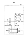
図1は、本発明の第1の実施形態に係る気化原料供給装置及び基板処理装置の一例を示した図である。図1において、気化原料供給装置250と、これを含む基板処理装置300が示されている。
図3は、本発明の第2の実施形態に係る基板処理装置301の一例を示した図である。なお、気化原料供給装置250については、第1の実施形態に係る気化原料供給装置250と同一であるので、各構成要素に同一の参照符号を付してその説明を省略する。
以下の実施形態では、第1及び第2の実施形態において説明した気化原料供給装置250及び基板処理装置300、301を、より具体的な基板処理装置に適用する例について説明する。第3の実施形態に係る基板処理装置302は、ALD(Atomic Layer Deposition、原子層成膜方法)成膜装置として構成されており、ALD法により成膜を行う装置である。
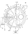
図7は、本発明の第4の実施形態に係る基板処理装置303の一例を示した図である。図7において、気化原料供給装置250に接続されたインジェクタ130が1本となり、インジェクタ130は、3つの領域となる室131〜133を有している。
図9は、本発明の第5の実施形態に係る基板処理装置のインジェクタ130aの一例を示した図である。第5の実施形態に係る基板処理装置は、図7に示した第4の実施形態に係る基板処理装置303と同様の平面構成を有するが、インジェクタ130aの構造のみが異なっている。
図10は、本発明の第6の実施形態に係る基板処理装置304の一例を示した図である。第6の実施形態に係る基板処理装置304においては、インジェクタ130bが1本である点は第4及び第5の実施形態に係る基板処理装置303と共通するが、ガス導入ポート1130が1個だけ容器本体12の外周に設けられている点で、第4及び第5の実施形態に係る基板処理装置303と異なっている。
図12は、第7の実施形態に係る基板処理装置のインジェクタ130cの一例を示した図である。第7の実施形態に係る基板処理装置は、図10に示した第6の実施形態に係る基板処理装置304と同様の平面構成を有するが、インジェクタ130cの構造のみが異なっている。
図13は、本発明の第8の実施形態に係る基板処理装置の一例を示した図である。第8の実施形態に係る基板処理装置は、気化原料供給装置250を縦型熱処理装置に適用した例について説明する。
図15は、本発明の第9の実施形態に係る基板処理装置のインジェクタ130eの一例を示した図である。第9の実施形態に係る基板処理装置は、図13に示した第8の実施形態に係る基板処理装置305と同様の全体構成を有するが、インジェクタ130eの構造のみが異なっている。
図16は、本発明の第10の実施形態に係る基板処理装置のインジェクタ131d〜133dの一例を示した図である。第10の実施形態に係る基板処理装置は、図13に示した第8の実施形態に係る基板処理装置305と類似した全体構成を有するが、図16に示されるように、気化原料を供給するインジェクタ131d〜133dが複数本に増加するとともに、各インジェクタ131d〜133dが処理容器422の高さ方向において異なる領域に気化原料を供給可能なようにガス吐出孔151〜153が設けられている点で、第8及び第9の実施形態に係る基板処理装置305と異なっている。
2 回転テーブル
111、112 オリフィス
121、121a〜121c、122、122a〜122c、1210〜1213、1220〜1223 隔壁
130、130a〜130e、131〜133 インジェクタ
131a〜131c、132a〜132c、133a〜133c 室
141、141a、141b、142、142a、142b、143、143a、143b ガス導入口
151〜153 ガス吐出孔
160 加熱タンク
161 貯留タンク
162 ヒータ
163 気化空間
171〜173 流量制御器
180 元配管
181〜183 分岐配管
191 原料配管
192 パージ配管
201〜203 バルブ
210 原料
220 ケーシング
250 気化原料供給装置
300〜305 基板処理装置
Claims (17)
- 固体又は液体の原料を気化して気化原料を生成する1つの気化原料生成手段と、
該気化原料生成手段に接続され、生成された前記気化原料を複数系統に分岐させる複数の分岐配管と、
該分岐配管の各々に個別に設けられた複数の流量制御器と、
基板を収容可能な処理容器と、
該処理容器内の複数の領域毎にガス導入口とガス吐出孔を備えたインジェクタと、を有し、
前記複数の分岐配管は、前記複数の領域毎に設けられた前記ガス導入口の各々に1対1に対応して接続されており、
前記インジェクタは、前記複数の領域毎に隔壁により分割して仕切られた複数の室を内部に有し、
前記隔壁の一部には連通口が設けられ、前記複数の室同士が連通可能に構成されている基板処理装置。 - 前記気化原料生成手段は、前記固体又は液体の原料を貯留する貯留タンクと、
該貯留タンクを加熱し、前記固体又は液体の原料を気化する加熱手段と、を有する請求項1に記載の基板処理装置。 - 前記貯留タンクは密閉容器からなり、生成した前記気化原料を前記貯留タンク内に保持可能である請求項2に記載の基板処理装置。
- 前記複数の分岐配管は、前記気化原料生成手段に1本の元配管を介して接続されている請求項1乃至3のいずれか一項に記載の基板処理装置。
- 前記元配管にはバルブが設けられている請求項4に記載の基板処理装置。
- 前記複数の分岐配管は、各々が前記気化原料生成手段に直接接続されている請求項1乃至3のいずれか一項に記載の基板処理装置。
- 前記複数の分岐配管の各々にバルブが設けられている請求項1乃至6のいずれか一項に記載の基板処理装置。
- 前記気化原料生成手段、前記複数の分岐配管及び前記複数の流量制御器を一体的に覆うケーシングを更に有する請求項1乃至7のいずれか一項に記載の基板処理装置。
- 前記ガス吐出孔は、前記複数の領域毎に複数個設けられている請求項1乃至8のいずれか一項に記載の基板処理装置。
- 前記インジェクタは、前記複数の領域毎に別個独立に設けられた複数のインジェクタを含む請求項1乃至9のいずれか一項に記載の基板処理装置。
- 前記複数の領域同士は、互いに重ならない領域を含む請求項1乃至10のいずれか一項に記載の基板処理装置。
- 隣接する前記複数の領域同士は、互いに重なる領域を含む請求項1乃至11のいずれか一項に記載の基板処理装置。
- 前記複数の室は、前記インジェクタの長手方向に沿って配置された請求項1乃至12のいずれか一項に記載の基板処理装置。
- 前記ガス導入口は、前記インジェクタの長手方向に平行な側面に設けられた請求項1乃至13のいずれか一項に記載の基板処理装置。
- 前記隔壁は、前記インジェクタ内で長手方向に沿って同心状に延びる部分を含み、
前記ガス導入口は、前記インジェクタ内に設けられた請求項1乃至14のいずれか一項に記載の基板処理装置。 - 前記複数の流量制御器の各々は、前記複数の分岐配管を介して接続された前記複数の領域毎に流量が設定されている請求項1乃至15のいずれか一項に記載の基板処理装置。
- 前記複数の流量制御器は、前記複数の領域毎に設定された前記流量に応じて最大設定流量の異なる流量制御器が用いられている請求項16に記載の基板処理装置。
Priority Applications (5)
| Application Number | Priority Date | Filing Date | Title |
|---|---|---|---|
| JP2016041317A JP6573559B2 (ja) | 2016-03-03 | 2016-03-03 | 気化原料供給装置及びこれを用いた基板処理装置 |
| TW106105664A TWI701736B (zh) | 2016-03-03 | 2017-02-21 | 利用氣化原料供給裝置的基板處理裝置 |
| KR1020170025676A KR102127550B1 (ko) | 2016-03-03 | 2017-02-27 | 기화 원료 공급 장치 및 이것을 사용한 기판 처리 장치 |
| US15/446,620 US20170253969A1 (en) | 2016-03-03 | 2017-03-01 | Vaporization raw material supplying device and substrate processing apparatus using the same |
| CN201710125017.3A CN107151793A (zh) | 2016-03-03 | 2017-03-03 | 气化原料供给装置和采用该供给装置的基板处理装置 |
Applications Claiming Priority (1)
| Application Number | Priority Date | Filing Date | Title |
|---|---|---|---|
| JP2016041317A JP6573559B2 (ja) | 2016-03-03 | 2016-03-03 | 気化原料供給装置及びこれを用いた基板処理装置 |
Publications (2)
| Publication Number | Publication Date |
|---|---|
| JP2017157744A JP2017157744A (ja) | 2017-09-07 |
| JP6573559B2 true JP6573559B2 (ja) | 2019-09-11 |
Family
ID=59723258
Family Applications (1)
| Application Number | Title | Priority Date | Filing Date |
|---|---|---|---|
| JP2016041317A Active JP6573559B2 (ja) | 2016-03-03 | 2016-03-03 | 気化原料供給装置及びこれを用いた基板処理装置 |
Country Status (5)
| Country | Link |
|---|---|
| US (1) | US20170253969A1 (ja) |
| JP (1) | JP6573559B2 (ja) |
| KR (1) | KR102127550B1 (ja) |
| CN (1) | CN107151793A (ja) |
| TW (1) | TWI701736B (ja) |
Families Citing this family (9)
| Publication number | Priority date | Publication date | Assignee | Title |
|---|---|---|---|---|
| KR20230113657A (ko) * | 2018-03-23 | 2023-07-31 | 가부시키가이샤 코쿠사이 엘렉트릭 | 기판 처리 장치, 반도체 장치의 제조 방법 및 프로그램 |
| US11274370B2 (en) * | 2018-05-24 | 2022-03-15 | Tokyo Electron Limited | Multiple zone gas injection for control of gas phase radicals |
| EP3599290A3 (en) | 2018-07-24 | 2020-06-03 | Lg Electronics Inc. | Chemical vapor deposition equipment for solar cell and deposition method thereof |
| JP6894482B2 (ja) * | 2019-09-12 | 2021-06-30 | 株式会社Kokusai Electric | 基板処理装置、半導体装置の製造方法、プログラム及び記録媒体 |
| JP7325350B2 (ja) * | 2020-02-03 | 2023-08-14 | 東京エレクトロン株式会社 | 成膜装置 |
| JP7273079B2 (ja) * | 2021-02-15 | 2023-05-12 | 株式会社Kokusai Electric | 基板処理装置、半導体装置の製造方法、プログラムおよび基板処理方法 |
| JP7420777B2 (ja) * | 2021-09-21 | 2024-01-23 | 株式会社Kokusai Electric | 半導体装置の製造方法、基板処理方法、基板処理装置及びプログラム |
| JP2023083853A (ja) * | 2021-12-06 | 2023-06-16 | キオクシア株式会社 | 半導体製造装置および半導体装置の製造方法 |
| WO2024062576A1 (ja) * | 2022-09-21 | 2024-03-28 | 株式会社Kokusai Electric | 基板処理装置、ノズル、半導体装置の製造方法、及びプログラム |
Family Cites Families (32)
| Publication number | Priority date | Publication date | Assignee | Title |
|---|---|---|---|---|
| JPS60184679A (ja) * | 1984-03-01 | 1985-09-20 | Nippon Telegr & Teleph Corp <Ntt> | 多層薄膜形成法及びそれに用いる装置 |
| JPS61254242A (ja) * | 1985-05-01 | 1986-11-12 | Sumitomo Electric Ind Ltd | 原料供給装置 |
| JP2668687B2 (ja) * | 1987-11-27 | 1997-10-27 | 富士通株式会社 | C v d 装 置 |
| JPH02205316A (ja) * | 1989-02-03 | 1990-08-15 | Sumitomo Metal Ind Ltd | エピタキシャル気相成長装置 |
| JPH04214870A (ja) * | 1990-05-08 | 1992-08-05 | Nec Corp | 化学気相成長装置 |
| DE69126122T2 (de) * | 1990-09-21 | 1997-08-28 | Fujitsu Ltd | Methode und apparat zum wachsen von verbindungshalbleiterkristallen |
| JP3128586B2 (ja) * | 1992-05-15 | 2001-01-29 | 東芝機械株式会社 | 薄膜成長装置 |
| JPH06295862A (ja) * | 1992-11-20 | 1994-10-21 | Mitsubishi Electric Corp | 化合物半導体製造装置及び有機金属材料容器 |
| JPH0945624A (ja) * | 1995-07-27 | 1997-02-14 | Tokyo Electron Ltd | 枚葉式の熱処理装置 |
| AU2001288225A1 (en) * | 2000-07-24 | 2002-02-05 | The University Of Maryland College Park | Spatially programmable microelectronics process equipment using segmented gas injection showerhead with exhaust gas recirculation |
| JP5034138B2 (ja) * | 2001-01-25 | 2012-09-26 | 東京エレクトロン株式会社 | 熱処理方法及び熱処理装置 |
| JP4553245B2 (ja) | 2004-09-30 | 2010-09-29 | 東京エレクトロン株式会社 | 気化器、成膜装置及び成膜方法 |
| US20060124169A1 (en) * | 2004-12-09 | 2006-06-15 | Tokyo Electron Limited | Gas supply unit, substrate processing apparatus, and supply gas setting method |
| JP4718274B2 (ja) * | 2005-08-25 | 2011-07-06 | 東京エレクトロン株式会社 | 半導体製造装置,半導体製造装置の流量補正方法,プログラム |
| JP4895167B2 (ja) * | 2006-01-31 | 2012-03-14 | 東京エレクトロン株式会社 | ガス供給装置,基板処理装置,ガス供給方法 |
| WO2007108401A1 (ja) * | 2006-03-20 | 2007-09-27 | Hitachi Kokusai Electric Inc. | 半導体装置の製造方法および基板処理装置 |
| US7562672B2 (en) * | 2006-03-30 | 2009-07-21 | Applied Materials, Inc. | Chemical delivery apparatus for CVD or ALD |
| JP5192214B2 (ja) * | 2007-11-02 | 2013-05-08 | 東京エレクトロン株式会社 | ガス供給装置、基板処理装置および基板処理方法 |
| JP5378706B2 (ja) * | 2008-05-22 | 2013-12-25 | 東京エレクトロン株式会社 | プラズマ処理装置及びそれに用いられる処理ガス供給装置 |
| JP5350824B2 (ja) * | 2009-02-03 | 2013-11-27 | 株式会社フジキン | 液体材料の気化供給システム |
| JP5216632B2 (ja) * | 2009-03-03 | 2013-06-19 | 東京エレクトロン株式会社 | 流体制御装置 |
| KR101094299B1 (ko) * | 2009-12-17 | 2011-12-19 | 삼성모바일디스플레이주식회사 | 선형 증발원 및 이를 포함하는 증착 장치 |
| US20120280369A1 (en) * | 2009-12-18 | 2012-11-08 | Hitachi Kokusai Electric Inc. | Method for manufacturing semiconductor device, substrate processing apparatus, and semiconductor device |
| JP5497423B2 (ja) * | 2009-12-25 | 2014-05-21 | 東京エレクトロン株式会社 | 成膜装置 |
| JP5689294B2 (ja) * | 2010-11-25 | 2015-03-25 | 東京エレクトロン株式会社 | 処理装置 |
| JP5755958B2 (ja) * | 2011-07-08 | 2015-07-29 | 株式会社フジキン | 半導体製造装置の原料ガス供給装置 |
| JP2013115208A (ja) * | 2011-11-28 | 2013-06-10 | Tokyo Electron Ltd | 気化原料供給装置、これを備える基板処理装置、及び気化原料供給方法 |
| JP2013197249A (ja) * | 2012-03-19 | 2013-09-30 | Hitachi Kokusai Electric Inc | 基板処理装置、半導体装置の製造方法及び流量制御方法 |
| TW201409688A (zh) * | 2012-08-03 | 2014-03-01 | Tokyo Electron Ltd | 形成化合物半導體膜之方法及設備 |
| JP6142629B2 (ja) * | 2013-03-29 | 2017-06-07 | 東京エレクトロン株式会社 | 原料ガス供給装置、成膜装置及び原料ガス供給方法 |
| JP2015185837A (ja) * | 2014-03-26 | 2015-10-22 | 東京エレクトロン株式会社 | 成膜装置 |
| CN103924214B (zh) * | 2014-04-25 | 2016-11-16 | 安徽亚格盛电子新材料有限公司 | 一种蒸汽输送mo源连续供应系统 |
-
2016
- 2016-03-03 JP JP2016041317A patent/JP6573559B2/ja active Active
-
2017
- 2017-02-21 TW TW106105664A patent/TWI701736B/zh active
- 2017-02-27 KR KR1020170025676A patent/KR102127550B1/ko active IP Right Grant
- 2017-03-01 US US15/446,620 patent/US20170253969A1/en not_active Abandoned
- 2017-03-03 CN CN201710125017.3A patent/CN107151793A/zh active Pending
Also Published As
| Publication number | Publication date |
|---|---|
| TW201801182A (zh) | 2018-01-01 |
| JP2017157744A (ja) | 2017-09-07 |
| TWI701736B (zh) | 2020-08-11 |
| CN107151793A (zh) | 2017-09-12 |
| US20170253969A1 (en) | 2017-09-07 |
| KR20170103663A (ko) | 2017-09-13 |
| KR102127550B1 (ko) | 2020-06-26 |
Similar Documents
| Publication | Publication Date | Title |
|---|---|---|
| JP6573559B2 (ja) | 気化原料供給装置及びこれを用いた基板処理装置 | |
| JP6590735B2 (ja) | 混合ガス複数系統供給システム及びこれを用いた基板処理装置 | |
| CN101748387B (zh) | 成膜装置 | |
| TWI494459B (zh) | 成膜裝置、成膜方法及記憶媒體 | |
| CN101660140B (zh) | 成膜装置及成膜方法、基板处理装置 | |
| US20180076021A1 (en) | Substrate processing apparatus | |
| US8808456B2 (en) | Film deposition apparatus and substrate process apparatus | |
| JP5195676B2 (ja) | 成膜装置、基板処理装置、成膜方法及び記憶媒体 | |
| CN101994101B (zh) | 成膜装置 | |
| US20140213068A1 (en) | Film deposition apparatus and film deposition method | |
| KR20100032328A (ko) | 성막 장치, 성막 방법 및 컴퓨터 판독 가능 기억 매체 | |
| CN101736318A (zh) | 成膜装置 | |
| CN101831632A (zh) | 成膜装置 | |
| KR20120092022A (ko) | 성막 장치 | |
| JP2007247066A (ja) | 回転サセプタを備える半導体処理装置 | |
| JP5886531B2 (ja) | 成膜方法および成膜装置 | |
| KR20100032326A (ko) | 성막 장치, 성막 방법 및 컴퓨터 판독 가능 기억 매체 | |
| JP2010056477A (ja) | 成膜装置及び基板処理装置 | |
| JP2009088232A (ja) | ガス供給装置 | |
| US10472719B2 (en) | Nozzle and substrate processing apparatus using same | |
| JP2006286716A (ja) | 半導体デバイスの製造方法 | |
| JP7274387B2 (ja) | 成膜装置及び成膜方法 | |
| TW201416481A (zh) | 成膜方法 | |
| KR20110047183A (ko) | 기판 처리 방법 및 기판 처리 장치 |
Legal Events
| Date | Code | Title | Description |
|---|---|---|---|
| A621 | Written request for application examination |
Free format text: JAPANESE INTERMEDIATE CODE: A621 Effective date: 20180809 |
|
| A977 | Report on retrieval |
Free format text: JAPANESE INTERMEDIATE CODE: A971007 Effective date: 20190425 |
|
| A131 | Notification of reasons for refusal |
Free format text: JAPANESE INTERMEDIATE CODE: A131 Effective date: 20190507 |
|
| A521 | Request for written amendment filed |
Free format text: JAPANESE INTERMEDIATE CODE: A523 Effective date: 20190702 |
|
| TRDD | Decision of grant or rejection written | ||
| A01 | Written decision to grant a patent or to grant a registration (utility model) |
Free format text: JAPANESE INTERMEDIATE CODE: A01 Effective date: 20190716 |
|
| A61 | First payment of annual fees (during grant procedure) |
Free format text: JAPANESE INTERMEDIATE CODE: A61 Effective date: 20190813 |
|
| R150 | Certificate of patent or registration of utility model |
Ref document number: 6573559 Country of ref document: JP Free format text: JAPANESE INTERMEDIATE CODE: R150 |
|
| R250 | Receipt of annual fees |
Free format text: JAPANESE INTERMEDIATE CODE: R250 |
|
| R250 | Receipt of annual fees |
Free format text: JAPANESE INTERMEDIATE CODE: R250 |