JP6499552B2 - 雑音耐性の高い回路基板及び電子装置 - Google Patents
雑音耐性の高い回路基板及び電子装置 Download PDFInfo
- Publication number
- JP6499552B2 JP6499552B2 JP2015164902A JP2015164902A JP6499552B2 JP 6499552 B2 JP6499552 B2 JP 6499552B2 JP 2015164902 A JP2015164902 A JP 2015164902A JP 2015164902 A JP2015164902 A JP 2015164902A JP 6499552 B2 JP6499552 B2 JP 6499552B2
- Authority
- JP
- Japan
- Prior art keywords
- ground pattern
- ground
- circuit board
- noise
- current
- Prior art date
- Legal status (The legal status is an assumption and is not a legal conclusion. Google has not performed a legal analysis and makes no representation as to the accuracy of the status listed.)
- Expired - Fee Related
Links
Images
Landscapes
- Structure Of Printed Boards (AREA)
- Noise Elimination (AREA)
Description
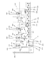
本発明の他の態様によると、前記雑音電流を遮るスリットが少なくとも2つ設けられており、当該スリットは前記第1のグランドパターンと前記電源装置につながるグランドラインとの接続部を当該第1のグランドパターンを流れる電流の方向に沿って挟む位置に設けられている。
本発明の他の態様によると、前記雑音電流を遮るスリットは、前記第1のグランドパターンを流れる電流の当該流れの方向に対し略直交する方向に設けられたスリットを含む。
本発明の他の態様によると、前記雑音電流を遮るスリットの少なくとも一つの両端部の近傍に、前記第1のグランドパターンと前記第2のグランドパターンとを交流的に接続する前記コンデンサが配されている。
本発明の他の態様は、上記いずれかの回路基板を備える電子装置である。
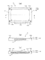
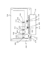
本電子装置10は、導電性材料(例えば、アルミニウム等の金属や導電性樹脂)から成るベース100aとカバー100bとがネジ102a〜102dにより固定されて構成される導電性の筐体100と、筐体100内に収容された回路基板104と、を備える。回路基板104は、電気回路部品106を含む複数の回路部品が搭載されて電子回路を構成しており、ベース100aに対し、ネジ108a〜108dにより固定されている。また、回路基板104には、当該回路基板104が構成する電子回路を外部の装置やデバイスに接続するためのコネクタ110が、筐体100から外部へ突き出た状態となるように搭載されている。なお、本明細書において「接続」とは、特にことわりのない限り、電気的に直流的に接続されることを意味するものとする。また、回路基板104に関し、図1に示す上面図側から見える面をオモテ面、これに対向する側のウラ面と称するものとする。
Claims (5)
- 回路基板であって、
電源装置につながるグランドラインに直接又は間接に直流的に接続される第1のグランドパターンと、
前記第1のグランドパターンに直接又は間接に交流的に接続されて、前記回路基板を収容する導電性の筐体に直流的に接続される第2のグランドパターンと、
を備え、
前記第1のグランドパターンの内部には、当該第1のグランドパターンを伝搬する雑音電流を遮る位置に、前記第1のグランドパターンの導体で囲まれたスリットが設けられており、少なくとも一つの前記スリットの少なくとも一つの端部近傍に前記第1のグランドパターンと前記第2のグランドパターンとを交流的に接続するコンデンサが配されている、
回路基板。 - 前記雑音電流を遮るスリットが少なくとも2つ設けられており、当該スリットは前記第1のグランドパターンと前記電源装置につながるグランドラインとの接続部を当該第1のグランドパターンを流れる電流の方向に沿って挟む位置に設けられている、
請求項1に記載の回路基板。 - 前記雑音電流を遮るスリットは、前記第1のグランドパターンを流れる電流の当該流れの方向に対し略直交する方向に設けられたスリットを含む、
請求項1又は2に記載の回路基板。 - 前記雑音電流を遮るスリットの少なくとも一つの両端部の近傍に、前記第1のグランドパターンと前記第2のグランドパターンとを交流的に接続する前記コンデンサが配されている、
請求項1ないし3に記載の回路基板。 - 請求項1ないし4のいずれか一項に記載の回路基板を備える電子装置。
Priority Applications (1)
| Application Number | Priority Date | Filing Date | Title |
|---|---|---|---|
| JP2015164902A JP6499552B2 (ja) | 2015-08-24 | 2015-08-24 | 雑音耐性の高い回路基板及び電子装置 |
Applications Claiming Priority (1)
| Application Number | Priority Date | Filing Date | Title |
|---|---|---|---|
| JP2015164902A JP6499552B2 (ja) | 2015-08-24 | 2015-08-24 | 雑音耐性の高い回路基板及び電子装置 |
Publications (2)
| Publication Number | Publication Date |
|---|---|
| JP2017045761A JP2017045761A (ja) | 2017-03-02 |
| JP6499552B2 true JP6499552B2 (ja) | 2019-04-10 |
Family
ID=58210073
Family Applications (1)
| Application Number | Title | Priority Date | Filing Date |
|---|---|---|---|
| JP2015164902A Expired - Fee Related JP6499552B2 (ja) | 2015-08-24 | 2015-08-24 | 雑音耐性の高い回路基板及び電子装置 |
Country Status (1)
| Country | Link |
|---|---|
| JP (1) | JP6499552B2 (ja) |
Family Cites Families (4)
| Publication number | Priority date | Publication date | Assignee | Title |
|---|---|---|---|---|
| JP3581971B2 (ja) * | 1996-05-22 | 2004-10-27 | 株式会社ボッシュオートモーティブシステム | 車載用コントロールユニットのemi用接地構造 |
| JP2005311081A (ja) * | 2004-04-21 | 2005-11-04 | D & M Holdings Inc | 基板回路装置、受信装置及び送信装置 |
| JP5039356B2 (ja) * | 2006-10-13 | 2012-10-03 | 三菱重工業株式会社 | 制御基板および電動圧縮機の制御装置ならびに電動圧縮機 |
| JP5740427B2 (ja) * | 2013-03-29 | 2015-06-24 | 本田技研工業株式会社 | 回路基板を備える制御装置 |
-
2015
- 2015-08-24 JP JP2015164902A patent/JP6499552B2/ja not_active Expired - Fee Related
Also Published As
| Publication number | Publication date |
|---|---|
| JP2017045761A (ja) | 2017-03-02 |
Similar Documents
| Publication | Publication Date | Title |
|---|---|---|
| JP6719021B2 (ja) | 電力変換装置 | |
| US20200045815A1 (en) | Circuit board and electronic device including the same | |
| JP2007149999A (ja) | 回路接続構造およびプリント回路板 | |
| WO2020066192A1 (ja) | 電子制御装置 | |
| JP6076174B2 (ja) | 雑音耐性の高い制御装置 | |
| CN105917567A (zh) | 功率转换器用的控制器 | |
| JP4967164B2 (ja) | 多層プリント配線板及びそれを用いた電子機器 | |
| JP6499552B2 (ja) | 雑音耐性の高い回路基板及び電子装置 | |
| JP6521682B2 (ja) | 回路部品間の干渉を防止し得る回路基板、及び当該回路基板備える電子装置 | |
| JP6513517B2 (ja) | グランド雑音に対する耐性の高い回路基板、及び当該回路基板を備える電子装置 | |
| JP7373705B2 (ja) | 回路基板、電子機器 | |
| US12432845B2 (en) | Vehicle-mounted electronic control device | |
| JP4735670B2 (ja) | プリント基板および画像処理装置 | |
| JP6389132B2 (ja) | 電子装置 | |
| US11523497B2 (en) | Electric power conversion apparatus and electric power steering apparatus using the same | |
| US12526913B2 (en) | Electronic device | |
| JP6373912B2 (ja) | ノイズフィルタ、及び当該ノイズフィルタが形成された回路基板 | |
| CN106535544B (zh) | 电气设备以及电力转换装置 | |
| JP6236892B2 (ja) | 表示装置 | |
| JP5966767B2 (ja) | 車両制御用回路基板 | |
| CN207519067U (zh) | 功率模块 | |
| TWI672865B (zh) | 電連接器 | |
| JP6546793B2 (ja) | プリント回路基板 | |
| JP2018207019A (ja) | プリント回路基板ユニット、プリント回路基板の接続方法 | |
| JP5454991B2 (ja) | ランド構造 |
Legal Events
| Date | Code | Title | Description |
|---|---|---|---|
| RD02 | Notification of acceptance of power of attorney |
Free format text: JAPANESE INTERMEDIATE CODE: A7422 Effective date: 20170714 |
|
| RD04 | Notification of resignation of power of attorney |
Free format text: JAPANESE INTERMEDIATE CODE: A7424 Effective date: 20170726 |
|
| A621 | Written request for application examination |
Free format text: JAPANESE INTERMEDIATE CODE: A621 Effective date: 20171129 |
|
| A977 | Report on retrieval |
Free format text: JAPANESE INTERMEDIATE CODE: A971007 Effective date: 20180816 |
|
| A131 | Notification of reasons for refusal |
Free format text: JAPANESE INTERMEDIATE CODE: A131 Effective date: 20180828 |
|
| A521 | Request for written amendment filed |
Free format text: JAPANESE INTERMEDIATE CODE: A523 Effective date: 20181012 |
|
| TRDD | Decision of grant or rejection written | ||
| A01 | Written decision to grant a patent or to grant a registration (utility model) |
Free format text: JAPANESE INTERMEDIATE CODE: A01 Effective date: 20190312 |
|
| A61 | First payment of annual fees (during grant procedure) |
Free format text: JAPANESE INTERMEDIATE CODE: A61 Effective date: 20190315 |
|
| R150 | Certificate of patent or registration of utility model |
Ref document number: 6499552 Country of ref document: JP Free format text: JAPANESE INTERMEDIATE CODE: R150 |
|
| LAPS | Cancellation because of no payment of annual fees |