JP6499552B2 - Circuit board and electronic device having high noise resistance - Google Patents
Circuit board and electronic device having high noise resistance Download PDFInfo
- Publication number
- JP6499552B2 JP6499552B2 JP2015164902A JP2015164902A JP6499552B2 JP 6499552 B2 JP6499552 B2 JP 6499552B2 JP 2015164902 A JP2015164902 A JP 2015164902A JP 2015164902 A JP2015164902 A JP 2015164902A JP 6499552 B2 JP6499552 B2 JP 6499552B2
- Authority
- JP
- Japan
- Prior art keywords
- ground pattern
- ground
- circuit board
- noise
- current
- Prior art date
- Legal status (The legal status is an assumption and is not a legal conclusion. Google has not performed a legal analysis and makes no representation as to the accuracy of the status listed.)
- Expired - Fee Related
Links
Images
Landscapes
- Structure Of Printed Boards (AREA)
- Noise Elimination (AREA)
Description
本発明は、電子回路を構成する回路基板及び当該回路基板を備える電子装置に関し、特に、電源装置につながるグランドラインにおけるグランド電位の変動(グランド雑音)に対する耐性の高い回路基板及び当該回路基板を備える電子装置に関する。 The present invention relates to a circuit board constituting an electronic circuit and an electronic device including the circuit board, and more particularly, to a circuit board having high resistance against ground potential fluctuation (ground noise) in a ground line connected to a power supply device, and the circuit board. The present invention relates to an electronic device.
電子回路を構成する回路基板を備える電子装置を、輻射雑音が存在する環境下で使用する場合、当該輻射雑音に起因して、当該電子装置と電源装置とをつなぐグランドラインにグランド電位の変動(グランド雑音)が発生し、当該グランド雑音が電子装置に流入することで、当該電子装置の動作が不安定なものとなり得る。 When an electronic device including a circuit board that constitutes an electronic circuit is used in an environment where radiation noise exists, fluctuations in the ground potential due to the radiation noise on the ground line connecting the electronic device and the power supply device ( When the ground noise is generated and the ground noise flows into the electronic device, the operation of the electronic device can be unstable.
従来、電源装置につながるグランドラインから進入するグランド雑音の影響を低減する技術として、回路基板を導電性の筐体内に収容し、回路基板上に形成されたグランドパターンを、コンデンサを介して筐体に接続することで、グランドパターンに流入したグランド雑音を筐体外部(例えば、当該筐体が取り付けられた導電性の外部構造物)へ排出する電子装置が知られている。また、他の技術として、多層プリント配線基板の表面層にアナログ入出力端子である外部接続部(コネクタ)と、アナログ回路と、アナロググランドと、デジタル回路とが形成され、中間層に基準電位を与えるデジタルグランドプレーンが形成され、外部接続部の近傍の、アナロググランド電位とデジタルグランド電位が同一である位置で、上記アナロググランドとデジタルグランドがコンデンサにより接続される、プリント配線基板が知られている(特許文献1参照)。このプリント配線基板では、外部接続部から進入するノイズが、上記コンデンサを介して即座にデジタルグランドプレーンに導かれるため、アナロググランドに対する当該ノイズの影響が防止される。 Conventionally, as a technique for reducing the influence of ground noise entering from a ground line connected to a power supply device, a circuit board is accommodated in a conductive casing, and a ground pattern formed on the circuit board is connected to the casing via a capacitor. There is known an electronic device that discharges ground noise that has flowed into the ground pattern to the outside of the housing (for example, a conductive external structure to which the housing is attached) by connecting to the ground pattern. As another technique, an external connection part (connector) that is an analog input / output terminal, an analog circuit, an analog ground, and a digital circuit are formed on the surface layer of the multilayer printed wiring board, and a reference potential is applied to the intermediate layer. A printed wiring board is known in which a digital ground plane is formed and the analog ground and the digital ground are connected by a capacitor at a position in the vicinity of the external connection portion where the analog ground potential and the digital ground potential are the same. (See Patent Document 1). In this printed wiring board, noise entering from the external connection portion is immediately guided to the digital ground plane via the capacitor, so that the influence of the noise on the analog ground is prevented.
しかしながら、上記従来の技術では、コンデンサのみによってグランド雑音が除去される構成となっているため、その除去効果には限界があり、当該コンデンサによって排除しきれなかったグランド雑音が、回路基板上に構成された電子回路の動作を不安定にさせる事態が生じ得る。 However, since the conventional technology has a configuration in which ground noise is removed only by a capacitor, its removal effect is limited, and ground noise that cannot be completely eliminated by the capacitor is configured on the circuit board. There may be a situation where the operation of the electronic circuit is made unstable.
例えば、このようなグランド雑音は、上記のように輻射雑音に起因して生ずるほか、電源装置に複数の電子装置が接続される場合には、自装置以外の他の電子装置のグランド電流が変動することによっても生じ得るものであり、雑音環境下において多くの電子装置が協働して機能するような用途、例えば、それぞれ異なる制御対象を制御する複数のECU(電子制御装置、Electronic Control Unit)で構成される車両制御システムにおいては、極めて大きなグランド雑音が発生し得る。このため、このようなシステムに用いられる電子装置では、でき得る限り高いグランド雑音耐性を持つことが期待される。 For example, such ground noise is caused by radiation noise as described above, and when a plurality of electronic devices are connected to the power supply device, the ground current of other electronic devices other than the own device fluctuates. In other applications where many electronic devices work together in a noisy environment, for example, multiple ECUs (Electronic Control Units) that control different objects to be controlled In the vehicle control system configured by the above, extremely large ground noise can be generated. For this reason, an electronic device used in such a system is expected to have the highest possible ground noise resistance.
上記背景より、回路基板及び当該回路基板を備える電子装置において、外来輻射雑音等に起因して電源装置につながるグランドラインから流入するグランド雑音の影響を効果的に抑制し得る構成の実現が望まれている。 From the above background, in a circuit board and an electronic device including the circuit board, it is desired to realize a configuration that can effectively suppress the influence of ground noise flowing from a ground line connected to a power supply device due to external radiation noise or the like. ing.
本発明の一の態様は、電子回路を構成する回路部品が搭載された回路基板であって、電源装置につながるグランドラインに直接又は間接に直流的に接続される第1のグランドパターンと、前記第1のグランドパターンに直接又は間接に交流的に接続されて、前記回路基板を収容する導電性の筐体に直流的に接続される第2のグランドパターンと、を備え、前記第1のグランドパターンの内部には、当該第1のグランドパターンを伝搬する雑音電流を遮る位置に、前記第1のグランドパターンの導体で囲まれたスリットが設けられており、少なくとも一つの前記スリットの少なくとも一つの端部近傍に前記第1のグランドパターンと前記第2のグランドパターンとを交流的に接続するコンデンサが配されている。
本発明の他の態様によると、前記雑音電流を遮るスリットが少なくとも2つ設けられており、当該スリットは前記第1のグランドパターンと前記電源装置につながるグランドラインとの接続部を当該第1のグランドパターンを流れる電流の方向に沿って挟む位置に設けられている。
本発明の他の態様によると、前記雑音電流を遮るスリットは、前記第1のグランドパターンを流れる電流の当該流れの方向に対し略直交する方向に設けられたスリットを含む。
本発明の他の態様によると、前記雑音電流を遮るスリットの少なくとも一つの両端部の近傍に、前記第1のグランドパターンと前記第2のグランドパターンとを交流的に接続する前記コンデンサが配されている。
本発明の他の態様は、上記いずれかの回路基板を備える電子装置である。
One aspect of the present invention is a circuit board on which circuit components constituting an electronic circuit are mounted, the first ground pattern directly or indirectly connected to a ground line connected to a power supply device in direct current, and A second ground pattern that is directly or indirectly connected to the first ground pattern in an alternating current manner and connected in a direct current to a conductive casing that houses the circuit board. Inside the pattern , a slit surrounded by the conductor of the first ground pattern is provided at a position that blocks a noise current propagating through the first ground pattern, and at least one of the at least one slit is provided. A capacitor for alternatingly connecting the first ground pattern and the second ground pattern is disposed in the vicinity of the end.
According to another aspect of the present invention, at least two slits for blocking the noise current are provided, and the slits connect a connection portion between the first ground pattern and a ground line connected to the power supply device. It is provided at a position sandwiched along the direction of the current flowing through the ground pattern.
According to another aspect of the present invention, the slit for blocking the noise current includes a slit provided in a direction substantially orthogonal to the direction of the flow of the current flowing through the first ground pattern.
According to another aspect of the present invention, the capacitor for alternatingly connecting the first ground pattern and the second ground pattern is disposed in the vicinity of at least one end of the slit that blocks the noise current. ing.
Another aspect of the present invention is an electronic device including any one of the above circuit boards.
以下、図面を参照して、本発明の実施の形態を説明する。本発明の実施形態としてここに示した回路基板及び電子装置は、例えば車両に搭載されて当該車両の動作の少なくとも一つを制御する制御回路が構成された回路基板を備える電子装置である。ただし、本回路基板及び本電子装置の構成は、これに限らず、他の用途を含め、広く一般に用いられている回路基板及び電子装置に同様に適用することができる。 Embodiments of the present invention will be described below with reference to the drawings. The circuit board and the electronic device shown here as embodiments of the present invention are electronic devices including a circuit board that is mounted on a vehicle, for example, and configured with a control circuit that controls at least one of the operations of the vehicle. However, the configurations of the circuit board and the electronic device are not limited to this, and can be similarly applied to widely used circuit boards and electronic devices including other uses.
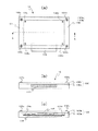
図1は、本発明の一実施形態に係る電子装置の構成を示す図である。図1(a)は本電子装置10の上面図、図1(b)は正面図、図1(c)はAA断面矢視図である。
本電子装置10は、導電性材料(例えば、アルミニウム等の金属や導電性樹脂)から成るベース100aとカバー100bとがネジ102a〜102dにより固定されて構成される導電性の筐体100と、筐体100内に収容された回路基板104と、を備える。回路基板104は、電気回路部品106を含む複数の回路部品が搭載されて電子回路を構成しており、ベース100aに対し、ネジ108a〜108dにより固定されている。また、回路基板104には、当該回路基板104が構成する電子回路を外部の装置やデバイスに接続するためのコネクタ110が、筐体100から外部へ突き出た状態となるように搭載されている。なお、本明細書において「接続」とは、特にことわりのない限り、電気的に直流的に接続されることを意味するものとする。また、回路基板104に関し、図1に示す上面図側から見える面をオモテ面、これに対向する側のウラ面と称するものとする。
FIG. 1 is a diagram illustrating a configuration of an electronic device according to an embodiment of the present invention. 1A is a top view of the
The
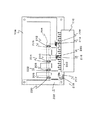
図2は、回路基板104のオモテ面の詳細を示す図である。なお、記載を簡略化して理解を容易にするため、図2においては電気回路部品106の記載を省略している。回路基板104のオモテ面には、外部の電源装置(不図示)のグランド端子からのグランドラインに接続されるコネクタ110の6本のピン(グランドピン)200に接続された第1のグランドパターンであるグランドパターン202が形成されている。すなわち、グランドパターン202は、回路基板104上に構成される電子回路に電源装置から供給された電流が当該電源装置へ還流する際のグランド電流が流れるグランドパターンである。
FIG. 2 is a diagram showing details of the front side of the
また、回路基板104のウラ面には、筐体100のベース100aと電気的に接続される第2のグランドパターンであるグランドパターン204(図示点線)が形成されている。これにより、グランドパターン204に流入した電流は、導電性の筐体100を介して、例えば当該筐体100が取り付けられている導電性の外部構造物へ流れ出る。
Further, a ground pattern 204 (dotted line in the drawing), which is a second ground pattern electrically connected to the
また、回路基板104のウラ面には、グランドパターン202とビア206、208、210、212、214、216、218を介してそれぞれ直流的に接続されたグランドパターン220、222、224、226、228、230、232が設けられている。
In addition, the
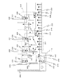
図3は、図2に示す回路基板104の部分詳細図であり、コネクタ110のグランドピン200及びその周辺部分が拡大して示されている。図示実線矢印は、グランドパターン202の各部を流れる電流のおおよその方向を示したものであり、図示破線矢印は、グランドピン200から流入した雑音電流の伝搬方向を示したものである。すなわち、一般に、高周波成分を持つ雑音電流(高周波電流)は回路基板上のグランドパターン内において直進性を有しており、図示破線矢印はその伝搬方向を表現したものである。
FIG. 3 is a partial detail view of the
本実施形態では、特に、第1のグランドパターンであるグランドパターン202内を伝搬する雑音電流をそれぞれ遮る位置にスリット300、302、304、306、308、310、312が設けられている。これにより、各スリット300〜312を挟んでそれぞれグランドピン200と対向する側のグランドパターン202の領域への雑音電流の伝搬が阻止される。
In the present embodiment,
また、各スリット300、302、304、306、308、310、312の一方又は両方の端部近傍においてグランドパターン220、222、224、226、228、230、232を介してグランドパターン202とグランドパターン204とを交流的に接続するためのコンデンサ320、322、324、326、328、330、332、334が配されている。
In addition, in the vicinity of one or both ends of each
これにより、各スリット300〜312を迂回して進もうとする雑音電流は、それぞれコンデンサ320〜334を介して(及びグランドパターン220〜232を介して)、グランドパターン204へ流れ込み、最終的なグランドパターン204から導電性の筐体100のベース100aから本電子装置10の外部(例えば、当該筐体100が取り付けられた導電性の外部構造物)へ排出される。
As a result, noise currents that attempt to bypass each of the
また、本実施形態では、電源装置につながるグランドラインとグランドパターン202との接続部であるコネクタ110の6本のグランドピン200とグランドパターン202との接続点から、図示両側方に向かってグランドパターン202が延在していることから、少なくとも2つのスリット(例えばスリット304と308)が、当該接続部を電源装置につながるグランドラインとの接続部をグランドパターン202を流れる電流の方向に沿って挟む位置に設けられている。これにより、ブランドグランドピン200から流れ込んだ雑音電流の、グランドパターン202に沿った図示左右両方向の伝搬が効果的に阻止される。
Further, in the present embodiment, the ground pattern from the connection point of the six
また、本実施形態では、スリット300〜312は、当該スリットが配されたグランドパターン202内の各位置おいて、グランドパターン202を流れる電流の方向に対し略直交する方向に設けられている。雑音電流は、グランドパターン202を流れる電流(グランド電流)の方向と略同一の方向に伝搬するので、これにより雑音電流の伝搬を効果的に阻止することができる。
In the present embodiment, the
以上、説明したように、本実施形態の回路基板104は、電源装置に繋がるグランドラインに接続されたグランドパターン202と、導電性の筐体に直流的に接続される第2のグランドパターン204とを備え、グランドパターン202には、当該グランドパターン202を伝搬する雑音電流を遮るスリット300〜312が設けられており、当該スリットの少なくとも一端の近傍に、グランドパターン202とグランドパターン204とを交流的に接続するコンデンサ320〜334が設けられている。これにより、本回路基板104では、グランド電流が流れるグランドパターン202内において、外部から流入した雑音電流が伝搬するのを効果的に阻止してこれを排除することができる。
As described above, the
なお、本実施形態では、グランドパターン202とグランドパターン204とが、グランドパターン220、222、224、226、228、230、232を介して間接的に、コンデンサ320、322、324、326、328、330、332、334により交流的に接続されるものとしたが、これに限らず、例えば回路基板104においてグランドパターン204がグランドパターン202とが同一面に形成される場合には、コンデンサ320、322、324、326、328、330、332、334の全部または一部が、グランドパターン202とグランドパターン204とを直接的に交流結合させるものとしてもよい。
In the present embodiment, the
10・・・電子装置、100・・・筐体、100a・・・ベース、100b・・・カバー、102a〜102d、108a〜108d・・・ネジ、104・・・回路基板、106・・・回路部品、110・・・コネクタ、200・・・グランドピン、202、204、220〜232・・・グランドパターン、206〜218・・・ビア、300〜312・・・スリット、320〜334・・・コンデンサ。
DESCRIPTION OF
Claims (5)
電源装置につながるグランドラインに直接又は間接に直流的に接続される第1のグランドパターンと、
前記第1のグランドパターンに直接又は間接に交流的に接続されて、前記回路基板を収容する導電性の筐体に直流的に接続される第2のグランドパターンと、
を備え、
前記第1のグランドパターンの内部には、当該第1のグランドパターンを伝搬する雑音電流を遮る位置に、前記第1のグランドパターンの導体で囲まれたスリットが設けられており、少なくとも一つの前記スリットの少なくとも一つの端部近傍に前記第1のグランドパターンと前記第2のグランドパターンとを交流的に接続するコンデンサが配されている、
回路基板。 A circuit board,
A first ground pattern connected directly or indirectly to a ground line connected to the power supply device in a direct current manner;
A second ground pattern that is directly or indirectly connected to the first ground pattern in an alternating current manner and connected in a direct current to a conductive housing that houses the circuit board;
With
Inside the first ground pattern, a slit surrounded by a conductor of the first ground pattern is provided at a position that blocks a noise current propagating through the first ground pattern, and at least one of the slits is provided. A capacitor for alternatingly connecting the first ground pattern and the second ground pattern is disposed in the vicinity of at least one end of the slit.
Circuit board.
請求項1に記載の回路基板。 At least two slits for blocking the noise current are provided, and the slits are connected to the ground line connected to the first ground pattern and the power supply device along the direction of the current flowing through the first ground pattern. It is provided at a position to sandwich,
The circuit board according to claim 1.
請求項1又は2に記載の回路基板。 The slit that blocks the noise current includes a slit provided in a direction substantially orthogonal to the direction of the current flowing through the first ground pattern.
The circuit board according to claim 1.
請求項1ないし3に記載の回路基板。 The capacitor for alternatingly connecting the first ground pattern and the second ground pattern is disposed in the vicinity of both ends of at least one slit that blocks the noise current.
The circuit board according to claim 1.
Priority Applications (1)
| Application Number | Priority Date | Filing Date | Title |
|---|---|---|---|
| JP2015164902A JP6499552B2 (en) | 2015-08-24 | 2015-08-24 | Circuit board and electronic device having high noise resistance |
Applications Claiming Priority (1)
| Application Number | Priority Date | Filing Date | Title |
|---|---|---|---|
| JP2015164902A JP6499552B2 (en) | 2015-08-24 | 2015-08-24 | Circuit board and electronic device having high noise resistance |
Publications (2)
| Publication Number | Publication Date |
|---|---|
| JP2017045761A JP2017045761A (en) | 2017-03-02 |
| JP6499552B2 true JP6499552B2 (en) | 2019-04-10 |
Family
ID=58210073
Family Applications (1)
| Application Number | Title | Priority Date | Filing Date |
|---|---|---|---|
| JP2015164902A Expired - Fee Related JP6499552B2 (en) | 2015-08-24 | 2015-08-24 | Circuit board and electronic device having high noise resistance |
Country Status (1)
| Country | Link |
|---|---|
| JP (1) | JP6499552B2 (en) |
Family Cites Families (4)
| Publication number | Priority date | Publication date | Assignee | Title |
|---|---|---|---|---|
| JP3581971B2 (en) * | 1996-05-22 | 2004-10-27 | 株式会社ボッシュオートモーティブシステム | EMI grounding structure for in-vehicle control unit |
| JP2005311081A (en) * | 2004-04-21 | 2005-11-04 | D & M Holdings Inc | Plated circuit device, receiving device and transmitting device |
| JP5039356B2 (en) * | 2006-10-13 | 2012-10-03 | 三菱重工業株式会社 | Control board, control device for electric compressor, and electric compressor |
| JP5740427B2 (en) * | 2013-03-29 | 2015-06-24 | 本田技研工業株式会社 | Control device provided with circuit board |
-
2015
- 2015-08-24 JP JP2015164902A patent/JP6499552B2/en not_active Expired - Fee Related
Also Published As
| Publication number | Publication date |
|---|---|
| JP2017045761A (en) | 2017-03-02 |
Similar Documents
| Publication | Publication Date | Title |
|---|---|---|
| JP6719021B2 (en) | Power converter | |
| US20200045815A1 (en) | Circuit board and electronic device including the same | |
| JP2007149999A (en) | Circuit connection structure and printed circuit board | |
| WO2020066192A1 (en) | Electronic control device | |
| JP6076174B2 (en) | Control device with high noise resistance | |
| CN105917567A (en) | Controller for power converter | |
| JP4967164B2 (en) | Multilayer printed wiring board and electronic device using the same | |
| JP6499552B2 (en) | Circuit board and electronic device having high noise resistance | |
| JP6521682B2 (en) | Circuit board capable of preventing interference between circuit components, and electronic device provided with the circuit board | |
| JP6513517B2 (en) | Circuit board highly resistant to ground noise, and electronic device provided with the circuit board | |
| JP7373705B2 (en) | circuit boards, electronic equipment | |
| US12432845B2 (en) | Vehicle-mounted electronic control device | |
| JP4735670B2 (en) | Printed circuit board and image processing apparatus | |
| JP6389132B2 (en) | Electronic equipment | |
| US11523497B2 (en) | Electric power conversion apparatus and electric power steering apparatus using the same | |
| US12526913B2 (en) | Electronic device | |
| JP6373912B2 (en) | Noise filter and circuit board on which the noise filter is formed | |
| CN106535544B (en) | Electrical device and power conversion device | |
| JP6236892B2 (en) | Display device | |
| JP5966767B2 (en) | Circuit board for vehicle control | |
| CN207519067U (en) | Power module | |
| TWI672865B (en) | Electric connector | |
| JP6546793B2 (en) | Printed circuit board | |
| JP2018207019A (en) | Printed circuit board unit and connection method of printed circuit board | |
| JP5454991B2 (en) | Land structure |
Legal Events
| Date | Code | Title | Description |
|---|---|---|---|
| RD02 | Notification of acceptance of power of attorney |
Free format text: JAPANESE INTERMEDIATE CODE: A7422 Effective date: 20170714 |
|
| RD04 | Notification of resignation of power of attorney |
Free format text: JAPANESE INTERMEDIATE CODE: A7424 Effective date: 20170726 |
|
| A621 | Written request for application examination |
Free format text: JAPANESE INTERMEDIATE CODE: A621 Effective date: 20171129 |
|
| A977 | Report on retrieval |
Free format text: JAPANESE INTERMEDIATE CODE: A971007 Effective date: 20180816 |
|
| A131 | Notification of reasons for refusal |
Free format text: JAPANESE INTERMEDIATE CODE: A131 Effective date: 20180828 |
|
| A521 | Request for written amendment filed |
Free format text: JAPANESE INTERMEDIATE CODE: A523 Effective date: 20181012 |
|
| TRDD | Decision of grant or rejection written | ||
| A01 | Written decision to grant a patent or to grant a registration (utility model) |
Free format text: JAPANESE INTERMEDIATE CODE: A01 Effective date: 20190312 |
|
| A61 | First payment of annual fees (during grant procedure) |
Free format text: JAPANESE INTERMEDIATE CODE: A61 Effective date: 20190315 |
|
| R150 | Certificate of patent or registration of utility model |
Ref document number: 6499552 Country of ref document: JP Free format text: JAPANESE INTERMEDIATE CODE: R150 |
|
| LAPS | Cancellation because of no payment of annual fees |