JP6479303B2 - 適応走査を有する走査顕微鏡 - Google Patents
適応走査を有する走査顕微鏡 Download PDFInfo
- Publication number
- JP6479303B2 JP6479303B2 JP2013097243A JP2013097243A JP6479303B2 JP 6479303 B2 JP6479303 B2 JP 6479303B2 JP 2013097243 A JP2013097243 A JP 2013097243A JP 2013097243 A JP2013097243 A JP 2013097243A JP 6479303 B2 JP6479303 B2 JP 6479303B2
- Authority
- JP
- Japan
- Prior art keywords
- area
- scan
- gray level
- pixels
- scanning
- Prior art date
- Legal status (The legal status is an assumption and is not a legal conclusion. Google has not performed a legal analysis and makes no representation as to the accuracy of the status listed.)
- Active
Links
- 230000003044 adaptive effect Effects 0.000 title description 2
- 238000000034 method Methods 0.000 claims description 43
- 239000002245 particle Substances 0.000 claims description 23
- 239000000463 material Substances 0.000 claims description 16
- 238000005259 measurement Methods 0.000 claims description 11
- 238000003860 storage Methods 0.000 claims description 8
- 230000004044 response Effects 0.000 claims description 4
- 239000000523 sample Substances 0.000 description 36
- 238000010884 ion-beam technique Methods 0.000 description 16
- 238000010894 electron beam technology Methods 0.000 description 14
- 210000004027 cell Anatomy 0.000 description 13
- 230000009977 dual effect Effects 0.000 description 12
- 150000002500 ions Chemical class 0.000 description 10
- 230000008569 process Effects 0.000 description 10
- 238000003384 imaging method Methods 0.000 description 9
- 238000012545 processing Methods 0.000 description 6
- 210000005253 yeast cell Anatomy 0.000 description 6
- 239000004593 Epoxy Substances 0.000 description 5
- 230000008901 benefit Effects 0.000 description 5
- 230000000875 corresponding effect Effects 0.000 description 5
- 238000011156 evaluation Methods 0.000 description 4
- 238000004519 manufacturing process Methods 0.000 description 3
- 239000000203 mixture Substances 0.000 description 3
- 230000015572 biosynthetic process Effects 0.000 description 2
- 230000001276 controlling effect Effects 0.000 description 2
- 230000008021 deposition Effects 0.000 description 2
- 238000011161 development Methods 0.000 description 2
- 230000018109 developmental process Effects 0.000 description 2
- 238000005530 etching Methods 0.000 description 2
- 238000011835 investigation Methods 0.000 description 2
- 210000003463 organelle Anatomy 0.000 description 2
- 238000005086 pumping Methods 0.000 description 2
- 230000009257 reactivity Effects 0.000 description 2
- 210000001519 tissue Anatomy 0.000 description 2
- ZCYVEMRRCGMTRW-UHFFFAOYSA-N 7553-56-2 Chemical compound [I] ZCYVEMRRCGMTRW-UHFFFAOYSA-N 0.000 description 1
- 102000011591 Cleavage And Polyadenylation Specificity Factor Human genes 0.000 description 1
- 108010076130 Cleavage And Polyadenylation Specificity Factor Proteins 0.000 description 1
- GYHNNYVSQQEPJS-UHFFFAOYSA-N Gallium Chemical compound [Ga] GYHNNYVSQQEPJS-UHFFFAOYSA-N 0.000 description 1
- 108010083687 Ion Pumps Proteins 0.000 description 1
- 230000001133 acceleration Effects 0.000 description 1
- 238000005452 bending Methods 0.000 description 1
- 239000012472 biological sample Substances 0.000 description 1
- 230000001413 cellular effect Effects 0.000 description 1
- 238000010276 construction Methods 0.000 description 1
- 230000002596 correlated effect Effects 0.000 description 1
- 238000005520 cutting process Methods 0.000 description 1
- 238000013480 data collection Methods 0.000 description 1
- 238000013479 data entry Methods 0.000 description 1
- 239000006185 dispersion Substances 0.000 description 1
- 239000008393 encapsulating agent Substances 0.000 description 1
- 230000007717 exclusion Effects 0.000 description 1
- 238000000605 extraction Methods 0.000 description 1
- 229910052733 gallium Inorganic materials 0.000 description 1
- 239000001963 growth medium Substances 0.000 description 1
- 238000002347 injection Methods 0.000 description 1
- 239000007924 injection Substances 0.000 description 1
- 229910052500 inorganic mineral Inorganic materials 0.000 description 1
- 239000011630 iodine Substances 0.000 description 1
- 229910052740 iodine Inorganic materials 0.000 description 1
- 239000012528 membrane Substances 0.000 description 1
- 229910052751 metal Inorganic materials 0.000 description 1
- 239000002184 metal Substances 0.000 description 1
- 229910021645 metal ion Inorganic materials 0.000 description 1
- 239000011707 mineral Substances 0.000 description 1
- 238000012986 modification Methods 0.000 description 1
- 230000004048 modification Effects 0.000 description 1
- 210000000056 organ Anatomy 0.000 description 1
- 150000002902 organometallic compounds Chemical class 0.000 description 1
- 239000002243 precursor Substances 0.000 description 1
- 230000000979 retarding effect Effects 0.000 description 1
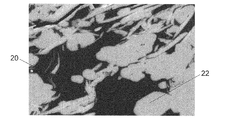
- 238000001878 scanning electron micrograph Methods 0.000 description 1
- 239000007787 solid Substances 0.000 description 1
- 238000000992 sputter etching Methods 0.000 description 1
- 230000003068 static effect Effects 0.000 description 1
- 238000006467 substitution reaction Methods 0.000 description 1
- 238000012546 transfer Methods 0.000 description 1
Images


Classifications
-
- G—PHYSICS
- G02—OPTICS
- G02B—OPTICAL ELEMENTS, SYSTEMS OR APPARATUS
- G02B21/00—Microscopes
- G02B21/0004—Microscopes specially adapted for specific applications
- G02B21/002—Scanning microscopes
-
- H—ELECTRICITY
- H01—ELECTRIC ELEMENTS
- H01J—ELECTRIC DISCHARGE TUBES OR DISCHARGE LAMPS
- H01J37/00—Discharge tubes with provision for introducing objects or material to be exposed to the discharge, e.g. for the purpose of examination or processing thereof
- H01J37/02—Details
- H01J37/22—Optical or photographic arrangements associated with the tube
- H01J37/222—Image processing arrangements associated with the tube
-
- H—ELECTRICITY
- H01—ELECTRIC ELEMENTS
- H01J—ELECTRIC DISCHARGE TUBES OR DISCHARGE LAMPS
- H01J37/00—Discharge tubes with provision for introducing objects or material to be exposed to the discharge, e.g. for the purpose of examination or processing thereof
- H01J37/26—Electron or ion microscopes; Electron or ion diffraction tubes
- H01J37/261—Details
- H01J37/265—Controlling the tube; circuit arrangements adapted to a particular application not otherwise provided, e.g. bright-field-dark-field illumination
-
- H—ELECTRICITY
- H01—ELECTRIC ELEMENTS
- H01J—ELECTRIC DISCHARGE TUBES OR DISCHARGE LAMPS
- H01J37/00—Discharge tubes with provision for introducing objects or material to be exposed to the discharge, e.g. for the purpose of examination or processing thereof
- H01J37/26—Electron or ion microscopes; Electron or ion diffraction tubes
- H01J37/28—Electron or ion microscopes; Electron or ion diffraction tubes with scanning beams
-
- H—ELECTRICITY
- H04—ELECTRIC COMMUNICATION TECHNIQUE
- H04N—PICTORIAL COMMUNICATION, e.g. TELEVISION
- H04N7/00—Television systems
- H04N7/18—Closed-circuit television [CCTV] systems, i.e. systems in which the video signal is not broadcast
-
- C—CHEMISTRY; METALLURGY
- C07—ORGANIC CHEMISTRY
- C07K—PEPTIDES
- C07K14/00—Peptides having more than 20 amino acids; Gastrins; Somatostatins; Melanotropins; Derivatives thereof
- C07K14/415—Peptides having more than 20 amino acids; Gastrins; Somatostatins; Melanotropins; Derivatives thereof from plants
-
- C—CHEMISTRY; METALLURGY
- C12—BIOCHEMISTRY; BEER; SPIRITS; WINE; VINEGAR; MICROBIOLOGY; ENZYMOLOGY; MUTATION OR GENETIC ENGINEERING
- C12N—MICROORGANISMS OR ENZYMES; COMPOSITIONS THEREOF; PROPAGATING, PRESERVING, OR MAINTAINING MICROORGANISMS; MUTATION OR GENETIC ENGINEERING; CULTURE MEDIA
- C12N15/00—Mutation or genetic engineering; DNA or RNA concerning genetic engineering, vectors, e.g. plasmids, or their isolation, preparation or purification; Use of hosts therefor
- C12N15/09—Recombinant DNA-technology
- C12N15/63—Introduction of foreign genetic material using vectors; Vectors; Use of hosts therefor; Regulation of expression
- C12N15/79—Vectors or expression systems specially adapted for eukaryotic hosts
- C12N15/82—Vectors or expression systems specially adapted for eukaryotic hosts for plant cells, e.g. plant artificial chromosomes (PACs)
- C12N15/8241—Phenotypically and genetically modified plants via recombinant DNA technology
- C12N15/8242—Phenotypically and genetically modified plants via recombinant DNA technology with non-agronomic quality (output) traits, e.g. for industrial processing; Value added, non-agronomic traits
- C12N15/8243—Phenotypically and genetically modified plants via recombinant DNA technology with non-agronomic quality (output) traits, e.g. for industrial processing; Value added, non-agronomic traits involving biosynthetic or metabolic pathways, i.e. metabolic engineering, e.g. nicotine, caffeine
- C12N15/8247—Phenotypically and genetically modified plants via recombinant DNA technology with non-agronomic quality (output) traits, e.g. for industrial processing; Value added, non-agronomic traits involving biosynthetic or metabolic pathways, i.e. metabolic engineering, e.g. nicotine, caffeine involving modified lipid metabolism, e.g. seed oil composition
-
- H—ELECTRICITY
- H01—ELECTRIC ELEMENTS
- H01J—ELECTRIC DISCHARGE TUBES OR DISCHARGE LAMPS
- H01J2237/00—Discharge tubes exposing object to beam, e.g. for analysis treatment, etching, imaging
- H01J2237/26—Electron or ion microscopes
- H01J2237/28—Scanning microscopes
- H01J2237/2813—Scanning microscopes characterised by the application
Landscapes
- Chemical & Material Sciences (AREA)
- Analytical Chemistry (AREA)
- Physics & Mathematics (AREA)
- Engineering & Computer Science (AREA)
- General Physics & Mathematics (AREA)
- Optics & Photonics (AREA)
- Computer Vision & Pattern Recognition (AREA)
- Multimedia (AREA)
- Signal Processing (AREA)
- Analysing Materials By The Use Of Radiation (AREA)
- Microscoopes, Condenser (AREA)
Description
上式で、
T=しきい値
CR=統合された走査の以前の走査における同じ画素に対する重みづけ定数
R=以前の走査における画素のビーム反応性の示数
CPSF=前表面係数(Provious Surface Factor)に対する重みづけ定数
前表面係数は、画素が、以前に走査した近隣の表面内の対象の領域内にある場合には=1、#ofpix<20の場合には=1/#ofpix、そのほかの場合には=0であり、#ofpixは、以前に走査した近隣の平面における対象の領域からの距離を画素数で表したものである。
SP.Px=既に走査した同じ平面の相互に関係づけられた画素
CV=局所画素分散に対する重みづけ定数
局所画素分散(Regionl Pixel Variance)=対象の画素の周囲のある画定されたエリア内、例えば100×100画素のエリア内の画素の分散
ε=ある画素を対象の画素ではないと誤って分類する所定の誤り率を与えるように設定された誤りマージン
さらに、好ましい一実施形態では、画素に対する測定誤差があるしきい値よりも低いときには、たとえ対象の構造体に対するものであっても、それぞれの画素のさらなる走査を停止する。すなわち、以前の表面からの情報、統合された走査の以前の走査からの情報および同じ平面内の以前に走査した画素からの情報を考慮することによって、その画素の値が所定の許容値よりも小さいと判定されたことをシステムが確信することができるときには、その画素を再び走査することはしない。
1014 イオン源
1016 集束カラム
1018 イオン・ビーム
1019 システム・コントローラ
1021 記憶装置
1022 試料
1024 可動X−Y−Zステージ
Claims (7)
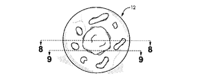
- 走査顕微鏡を使用して試料内の対象の構造体の画像を迅速に形成する方法であって、
前記試料の第1のエリアの最初の走査または最初の走査セットを実行して、前記第1のエリアに対応する一組の画素のそれぞれの画素の第1のグレー・レベル値を決定するステップと、
前記第1のグレー・レベル値を解析して、前記対象の構造体を表す前記第1のエリア内の第1の領域に対応する前記画素のサブセットを識別するステップと、
前記第1の領域に対応する前記画素のサブセットの画素についてのみ第2のグレー・レベル値を決定するために前記第1の領域の追加の走査を実行することによって、前記第1の領域に対応する画素のグレー・レベル測定値をより正確に決定するステップであり、前記第2のグレー・レベル値が、前記第1のグレー・レベル値を決定するのに使用した走査の回数よりも多くの回数の走査を統合することによって決定され、前記追加の走査は、前記最初の走査または最初の走査セットで収集された画素数よりも少ない画素についてグレー・レベルのデータを集める、ステップと
を含む方法。 - 前記第1の領域に対応する前記画素のサブセットを識別するステップが、前記第1のグレー・レベル値を第1のしきい値と比較することを含み、前記第1のしきい値が、前記第1のグレー・レベル値を決定するのに使用した走査の回数に依存し、
前記第1の領域に対応する画素のグレー・レベル測定値をより正確に決定するステップが、前記第2のグレー・レベルを複数の第2のしきい値と比較するステップを含み、複数の前記第2のしきい値が、前記追加の走査から除外する複数の画素を選択するのに用いられる、請求項1に記載の方法。 - 前記第1の領域に対応する前記画素のサブセットを識別するステップが、前記第1のグレー・レベル値を複数のしきい値と比較することを含み、複数の前記しきい値が、複数の画素のグレー・レベルの確率密度関数に依存する、請求項1に記載の方法。
- 前記追加の走査を実行するステップが、前記第2のグレー・レベル値を解析して、前記対象の構造体を表す前記第1のエリア内の第2の領域に対応する前記画素のサブセットを識別するステップを含み、前記追加の走査を実行するステップがさらに、前記第2の領域の追加の走査を実行して、前記第2の領域に対応する前記画素のサブセットについてのみ第3のグレー・レベル値を決定するステップを含み、前記第3のグレー・レベル値が、前記第2のグレー・レベル値を決定するのに使用した走査の回数よりも多い回数の走査を統合することによって決定される、請求項1から3のいずれか一項に記載の方法。
- 前記第1のエリアを含む材料の層を前記試料から除去することによって第2のエリアを露出させるステップと、
前記第2のエリアの第2の領域を走査するステップであり、前記第2のエリアの第2の領域が、前記第2のエリア内において前記第1の領域に対応するステップと
をさらに含む、請求項1から4のいずれかに一項に記載の方法。 - 材料を漸進的に除去して新たなエリアを露出させるステップと、
新たなエリアが露出するたびに、それぞれの新たなエリアの限定された領域を走査するステップであり、前記限定された領域が、以前のエリア内の対応する領域に対応する複数の画素のグレー・レベル値を解析することによって決定されるステップと
をさらに含む、請求項5に記載の方法。 - 走査荷電粒子ビーム・システムであって、
荷電粒子源と、
荷電粒子ビームで試料を走査する偏向器と、
前記荷電粒子ビームを前記試料の表面に集束させるレンズと、
前記荷電粒子の衝突に反応した前記試料からの放出を検出する検出器と、
前記走査荷電粒子ビーム・システムの動作を制御するコンピュータと、
請求項1に記載の方法を実行するための命令を記憶したコンピュータ可読記憶装置と
を備える走査荷電粒子ビーム・システム。
Applications Claiming Priority (2)
| Application Number | Priority Date | Filing Date | Title |
|---|---|---|---|
| US13/474,176 US9041793B2 (en) | 2012-05-17 | 2012-05-17 | Scanning microscope having an adaptive scan |
| US13/474,176 | 2012-05-17 |
Publications (3)
| Publication Number | Publication Date |
|---|---|
| JP2013243128A JP2013243128A (ja) | 2013-12-05 |
| JP2013243128A5 JP2013243128A5 (ja) | 2016-06-23 |
| JP6479303B2 true JP6479303B2 (ja) | 2019-03-06 |
Family
ID=48366268
Family Applications (1)
| Application Number | Title | Priority Date | Filing Date |
|---|---|---|---|
| JP2013097243A Active JP6479303B2 (ja) | 2012-05-17 | 2013-05-07 | 適応走査を有する走査顕微鏡 |
Country Status (4)
| Country | Link |
|---|---|
| US (1) | US9041793B2 (ja) |
| EP (1) | EP2665083A3 (ja) |
| JP (1) | JP6479303B2 (ja) |
| CN (1) | CN103424419B (ja) |
Families Citing this family (12)
| Publication number | Priority date | Publication date | Assignee | Title |
|---|---|---|---|---|
| DE102007045897A1 (de) * | 2007-09-26 | 2009-04-09 | Carl Zeiss Microimaging Gmbh | Verfahren zur mikroskopischen dreidimensionalen Abbildung einer Probe |
| IN2014MN02311A (ja) * | 2012-05-29 | 2015-08-07 | Univ Macquarie | |
| EP2879156A1 (en) * | 2013-12-02 | 2015-06-03 | Fei Company | Charged-particle microscopy with enhanced electron detection |
| US9502211B1 (en) | 2015-05-03 | 2016-11-22 | Fei Company | Adaptive scanning for particle size using directed beam signal analysis |
| US10535131B2 (en) * | 2015-11-18 | 2020-01-14 | Kla-Tencor Corporation | Systems and methods for region-adaptive defect detection |
| JP6522535B2 (ja) * | 2016-02-29 | 2019-05-29 | 富士フイルム株式会社 | 細胞観察装置および方法 |
| US11506877B2 (en) | 2016-11-10 | 2022-11-22 | The Trustees Of Columbia University In The City Of New York | Imaging instrument having objective axis and light sheet or light beam projector axis intersecting at less than 90 degrees |
| CN111107973A (zh) * | 2017-10-16 | 2020-05-05 | 惠普发展公司,有限责任合伙企业 | 3d打印机 |
| EP3598474A1 (en) | 2018-07-19 | 2020-01-22 | FEI Company | Adaptive specimen image acquisition using an artificial neural network |
| US20200118786A1 (en) * | 2018-10-15 | 2020-04-16 | Applied Materials, Inc. | System and method for selective autofocus |
| EP3948923A4 (en) * | 2019-03-28 | 2022-12-21 | Massachusetts Institute of Technology | SYSTEM AND METHOD FOR LEARNING-GUIDED ELECTRONIC MICROSCOPY |
| CN113804918B (zh) * | 2021-08-30 | 2023-12-26 | 广州大学 | 基于感兴趣区域的电化学扫描成像方法、装置及介质 |
Family Cites Families (35)
| Publication number | Priority date | Publication date | Assignee | Title |
|---|---|---|---|---|
| JPH0340351A (ja) * | 1989-07-05 | 1991-02-21 | Nippon Steel Corp | 析出物の解析方法および装置 |
| JP3037006B2 (ja) * | 1992-12-25 | 2000-04-24 | 日本電子株式会社 | 走査電子顕微鏡における自動画像調整方法 |
| US5435850A (en) | 1993-09-17 | 1995-07-25 | Fei Company | Gas injection system |
| US5851413A (en) | 1996-06-19 | 1998-12-22 | Micrion Corporation | Gas delivery systems for particle beam processing |
| JPH1092367A (ja) * | 1996-07-24 | 1998-04-10 | Jeol Ltd | 走査電子顕微鏡 |
| EP1168088A4 (en) * | 1999-03-03 | 2004-09-29 | Matsushita Electric Ind Co Ltd | R LINK SINE FOR TONER, TONER AND LECTROPHOTOGRAPHY |
| JP2001304842A (ja) * | 2000-04-25 | 2001-10-31 | Hitachi Ltd | パターン検査方法及びその装置並びに基板の処理方法 |
| US6855929B2 (en) * | 2000-12-01 | 2005-02-15 | Ebara Corporation | Apparatus for inspection with electron beam, method for operating same, and method for manufacturing semiconductor device using former |
| EP1390814A2 (en) * | 2001-05-30 | 2004-02-25 | Nptest, Inc. | Sub-resolution alignment of images |
| US6889113B2 (en) | 2001-08-23 | 2005-05-03 | Fei Company | Graphical automated machine control and metrology |
| AU2003255332A1 (en) * | 2002-07-30 | 2004-02-23 | Steinbeis-Transferzentrum Analytische Elektronenmikroskopie, Biomedizin, Biotechnologie-Heidelberg | Method and apparatus for multiple labeling detection and evaluation of a plurality of particles |
| JP4249453B2 (ja) * | 2002-09-25 | 2009-04-02 | 大日本印刷株式会社 | Sem画像における特徴量算出方法 |
| JP5107506B2 (ja) * | 2002-11-12 | 2012-12-26 | エフ・イ−・アイ・カンパニー | 欠陥分析器 |
| US7496228B2 (en) * | 2003-06-13 | 2009-02-24 | Landwehr Val R | Method and system for detecting and classifying objects in images, such as insects and other arthropods |
| JP4587742B2 (ja) * | 2004-08-23 | 2010-11-24 | 株式会社日立ハイテクノロジーズ | 荷電粒子線顕微方法及び荷電粒子線応用装置 |
| US7348556B2 (en) | 2005-07-19 | 2008-03-25 | Fei Company | Method of measuring three-dimensional surface roughness of a structure |
| US20070031043A1 (en) * | 2005-08-02 | 2007-02-08 | Perz Cynthia B | System for and method of intelligently directed segmentation analysis for automated microscope systems |
| JP5600371B2 (ja) * | 2006-02-15 | 2014-10-01 | エフ・イ−・アイ・カンパニー | 荷電粒子ビーム処理のための保護層のスパッタリング・コーティング |
| JP4734148B2 (ja) * | 2006-03-14 | 2011-07-27 | 株式会社日立ハイテクノロジーズ | 試料観察方法,画像処理装置、及び荷電粒子線装置 |
| JP5147327B2 (ja) * | 2007-07-31 | 2013-02-20 | 株式会社日立ハイテクノロジーズ | 荷電粒子ビーム照射装置 |
| US8064678B2 (en) * | 2007-10-22 | 2011-11-22 | Genetix Corporation | Automated detection of cell colonies and coverslip detection using hough transforms |
| JP5296413B2 (ja) * | 2008-05-15 | 2013-09-25 | 株式会社日立ハイテクサイエンス | 複合荷電粒子ビーム装置を用いた断面画像取得方法および複合荷電粒子ビーム装置 |
| US20090296073A1 (en) * | 2008-05-28 | 2009-12-03 | Lam Research Corporation | Method to create three-dimensional images of semiconductor structures using a focused ion beam device and a scanning electron microscope |
| JP5066056B2 (ja) * | 2008-10-31 | 2012-11-07 | 株式会社日立ハイテクノロジーズ | 試料観察方法、及び電子顕微鏡 |
| US9123502B2 (en) * | 2009-05-20 | 2015-09-01 | Carl Zeiss Microscopy, Llc | Scan method |
| EP2433293B1 (en) * | 2009-05-20 | 2013-09-04 | Carl Zeiss Microscopy, LLC | Scan method |
| JP5739119B2 (ja) * | 2009-09-15 | 2015-06-24 | 株式会社日立ハイテクサイエンス | 断面加工観察装置 |
| JP5292348B2 (ja) * | 2010-03-26 | 2013-09-18 | 株式会社日立ハイテクノロジーズ | 複合荷電粒子線装置 |
| US8350237B2 (en) * | 2010-03-31 | 2013-01-08 | Fei Company | Automated slice milling for viewing a feature |
| JP2011233466A (ja) * | 2010-04-30 | 2011-11-17 | Jeol Ltd | 電子顕微鏡の分解能評価方法、プログラム、及び情報記憶媒体 |
| JP5690086B2 (ja) * | 2010-07-02 | 2015-03-25 | 株式会社キーエンス | 拡大観察装置 |
| EP2416165A1 (en) | 2010-08-04 | 2012-02-08 | FEI Company | Method of forming a 3D reconstruction of a sample using a scanning probe microscope |
| JP5396350B2 (ja) * | 2010-08-31 | 2014-01-22 | 株式会社日立ハイテクノロジーズ | 画像形成装置、及びコンピュータプログラム |
| US9275441B2 (en) * | 2011-04-12 | 2016-03-01 | Tripath Imaging, Inc. | Method for preparing quantitative video-microscopy and associated system |
| EP2584362A1 (en) | 2011-10-18 | 2013-04-24 | FEI Company | Scanning method for scanning a sample with a probe |
-
2012
- 2012-05-17 US US13/474,176 patent/US9041793B2/en active Active
-
2013
- 2013-05-07 JP JP2013097243A patent/JP6479303B2/ja active Active
- 2013-05-16 CN CN201310181310.3A patent/CN103424419B/zh active Active
- 2013-05-16 EP EP13167952.4A patent/EP2665083A3/en not_active Withdrawn
Also Published As
| Publication number | Publication date |
|---|---|
| CN103424419A (zh) | 2013-12-04 |
| JP2013243128A (ja) | 2013-12-05 |
| CN103424419B (zh) | 2019-08-06 |
| US9041793B2 (en) | 2015-05-26 |
| EP2665083A3 (en) | 2016-04-06 |
| EP2665083A2 (en) | 2013-11-20 |
| US20130307957A1 (en) | 2013-11-21 |
Similar Documents
| Publication | Publication Date | Title |
|---|---|---|
| JP6479303B2 (ja) | 適応走査を有する走査顕微鏡 | |
| US9852881B2 (en) | Scanning electron microscope system, pattern measurement method using same, and scanning electron microscope | |
| CN109765254B (zh) | 图案测量装置以及测量方法 | |
| US10290464B2 (en) | Charged particle beam device and pattern measurement device | |
| EP2482061B1 (en) | System and method for localization of large numbers of fluorescent markers in biological samples | |
| US10984981B2 (en) | Charged particle beam device having inspection scan direction based on scan with smaller dose | |
| JP6739553B2 (ja) | 荷電粒子線装置 | |
| CN102207472A (zh) | 用于观察特征的自动化片状铣削 | |
| JP7305422B2 (ja) | パターン評価システム及びパターン評価方法 | |
| US10128080B2 (en) | Three-dimensional imaging in charged-particle microscopy | |
| JP2015536457A (ja) | 自動化された鉱物分類 | |
| US11971372B2 (en) | Method of examining a sample using a charged particle microscope | |
| WO2010095392A1 (ja) | 試料観察方法および走査電子顕微鏡 | |
| JP5117080B2 (ja) | 試料観察条件設定方法及び装置、並びに試料観察方法及び装置 | |
| US10665420B2 (en) | Charged particle beam apparatus | |
| US8110799B2 (en) | Confocal secondary electron imaging | |
| JP2014106388A (ja) | 自動合焦点検出装置及びそれを備える荷電粒子線顕微鏡 | |
| JP2006172919A (ja) | 三次元形状解析機能を有する走査型電子顕微鏡 | |
| US11742177B2 (en) | Charged particle beam apparatus and control method thereof | |
| EP4369376A1 (en) | Improved transmission electron microscopy | |
| US20240144560A1 (en) | Training Method for Learning Apparatus, and Image Generation System | |
| JP6895344B2 (ja) | 荷電粒子線装置 | |
| JP2005166472A (ja) | 観察方法及び観察装置 | |
| KR20230018315A (ko) | 하전 입자선 장치의 촬상 화상에 따른 조건 결정 방법, 장치 및 프로그램 | |
| CN113785170A (zh) | 图案测量装置以及测量方法 |
Legal Events
| Date | Code | Title | Description |
|---|---|---|---|
| A521 | Request for written amendment filed |
Free format text: JAPANESE INTERMEDIATE CODE: A523 Effective date: 20160501 |
|
| A621 | Written request for application examination |
Free format text: JAPANESE INTERMEDIATE CODE: A621 Effective date: 20160501 |
|
| A977 | Report on retrieval |
Free format text: JAPANESE INTERMEDIATE CODE: A971007 Effective date: 20170207 |
|
| A131 | Notification of reasons for refusal |
Free format text: JAPANESE INTERMEDIATE CODE: A131 Effective date: 20170328 |
|
| A601 | Written request for extension of time |
Free format text: JAPANESE INTERMEDIATE CODE: A601 Effective date: 20170627 |
|
| A601 | Written request for extension of time |
Free format text: JAPANESE INTERMEDIATE CODE: A601 Effective date: 20170826 |
|
| A521 | Request for written amendment filed |
Free format text: JAPANESE INTERMEDIATE CODE: A523 Effective date: 20170928 |
|
| A131 | Notification of reasons for refusal |
Free format text: JAPANESE INTERMEDIATE CODE: A131 Effective date: 20180306 |
|
| A601 | Written request for extension of time |
Free format text: JAPANESE INTERMEDIATE CODE: A601 Effective date: 20180605 |
|
| A521 | Request for written amendment filed |
Free format text: JAPANESE INTERMEDIATE CODE: A523 Effective date: 20180801 |
|
| TRDD | Decision of grant or rejection written | ||
| A01 | Written decision to grant a patent or to grant a registration (utility model) |
Free format text: JAPANESE INTERMEDIATE CODE: A01 Effective date: 20190129 |
|
| A61 | First payment of annual fees (during grant procedure) |
Free format text: JAPANESE INTERMEDIATE CODE: A61 Effective date: 20190206 |
|
| R150 | Certificate of patent or registration of utility model |
Ref document number: 6479303 Country of ref document: JP Free format text: JAPANESE INTERMEDIATE CODE: R150 |
|
| R250 | Receipt of annual fees |
Free format text: JAPANESE INTERMEDIATE CODE: R250 |
|
| R250 | Receipt of annual fees |
Free format text: JAPANESE INTERMEDIATE CODE: R250 |
|
| R250 | Receipt of annual fees |
Free format text: JAPANESE INTERMEDIATE CODE: R250 |