JP6479303B2 - Scanning microscope with adaptive scanning - Google Patents
Scanning microscope with adaptive scanning Download PDFInfo
- Publication number
- JP6479303B2 JP6479303B2 JP2013097243A JP2013097243A JP6479303B2 JP 6479303 B2 JP6479303 B2 JP 6479303B2 JP 2013097243 A JP2013097243 A JP 2013097243A JP 2013097243 A JP2013097243 A JP 2013097243A JP 6479303 B2 JP6479303 B2 JP 6479303B2
- Authority
- JP
- Japan
- Prior art keywords
- area
- scan
- gray level
- pixels
- scanning
- Prior art date
- Legal status (The legal status is an assumption and is not a legal conclusion. Google has not performed a legal analysis and makes no representation as to the accuracy of the status listed.)
- Active
Links
- 230000003044 adaptive effect Effects 0.000 title description 2
- 238000000034 method Methods 0.000 claims description 43
- 239000002245 particle Substances 0.000 claims description 23
- 239000000463 material Substances 0.000 claims description 16
- 238000005259 measurement Methods 0.000 claims description 11
- 238000003860 storage Methods 0.000 claims description 8
- 230000004044 response Effects 0.000 claims description 4
- 239000000523 sample Substances 0.000 description 36
- 238000010884 ion-beam technique Methods 0.000 description 16
- 238000010894 electron beam technology Methods 0.000 description 14
- 210000004027 cell Anatomy 0.000 description 13
- 230000009977 dual effect Effects 0.000 description 12
- 150000002500 ions Chemical class 0.000 description 10
- 230000008569 process Effects 0.000 description 10
- 238000003384 imaging method Methods 0.000 description 9
- 238000012545 processing Methods 0.000 description 6
- 210000005253 yeast cell Anatomy 0.000 description 6
- 239000004593 Epoxy Substances 0.000 description 5
- 230000008901 benefit Effects 0.000 description 5
- 230000000875 corresponding effect Effects 0.000 description 5
- 238000011156 evaluation Methods 0.000 description 4
- 238000004519 manufacturing process Methods 0.000 description 3
- 239000000203 mixture Substances 0.000 description 3
- 230000015572 biosynthetic process Effects 0.000 description 2
- 230000001276 controlling effect Effects 0.000 description 2
- 230000008021 deposition Effects 0.000 description 2
- 238000011161 development Methods 0.000 description 2
- 230000018109 developmental process Effects 0.000 description 2
- 238000005530 etching Methods 0.000 description 2
- 238000011835 investigation Methods 0.000 description 2
- 210000003463 organelle Anatomy 0.000 description 2
- 238000005086 pumping Methods 0.000 description 2
- 230000009257 reactivity Effects 0.000 description 2
- 210000001519 tissue Anatomy 0.000 description 2
- ZCYVEMRRCGMTRW-UHFFFAOYSA-N 7553-56-2 Chemical compound [I] ZCYVEMRRCGMTRW-UHFFFAOYSA-N 0.000 description 1
- 102000011591 Cleavage And Polyadenylation Specificity Factor Human genes 0.000 description 1
- 108010076130 Cleavage And Polyadenylation Specificity Factor Proteins 0.000 description 1
- GYHNNYVSQQEPJS-UHFFFAOYSA-N Gallium Chemical compound [Ga] GYHNNYVSQQEPJS-UHFFFAOYSA-N 0.000 description 1
- 108010083687 Ion Pumps Proteins 0.000 description 1
- 230000001133 acceleration Effects 0.000 description 1
- 238000005452 bending Methods 0.000 description 1
- 239000012472 biological sample Substances 0.000 description 1
- 230000001413 cellular effect Effects 0.000 description 1
- 238000010276 construction Methods 0.000 description 1
- 230000002596 correlated effect Effects 0.000 description 1
- 238000005520 cutting process Methods 0.000 description 1
- 238000013480 data collection Methods 0.000 description 1
- 238000013479 data entry Methods 0.000 description 1
- 239000006185 dispersion Substances 0.000 description 1
- 239000008393 encapsulating agent Substances 0.000 description 1
- 230000007717 exclusion Effects 0.000 description 1
- 238000000605 extraction Methods 0.000 description 1
- 229910052733 gallium Inorganic materials 0.000 description 1
- 239000001963 growth medium Substances 0.000 description 1
- 238000002347 injection Methods 0.000 description 1
- 239000007924 injection Substances 0.000 description 1
- 229910052500 inorganic mineral Inorganic materials 0.000 description 1
- 239000011630 iodine Substances 0.000 description 1
- 229910052740 iodine Inorganic materials 0.000 description 1
- 239000012528 membrane Substances 0.000 description 1
- 229910052751 metal Inorganic materials 0.000 description 1
- 239000002184 metal Substances 0.000 description 1
- 229910021645 metal ion Inorganic materials 0.000 description 1
- 239000011707 mineral Substances 0.000 description 1
- 238000012986 modification Methods 0.000 description 1
- 230000004048 modification Effects 0.000 description 1
- 210000000056 organ Anatomy 0.000 description 1
- 150000002902 organometallic compounds Chemical class 0.000 description 1
- 239000002243 precursor Substances 0.000 description 1
- 230000000979 retarding effect Effects 0.000 description 1
- 238000001878 scanning electron micrograph Methods 0.000 description 1
- 239000007787 solid Substances 0.000 description 1
- 238000000992 sputter etching Methods 0.000 description 1
- 230000003068 static effect Effects 0.000 description 1
- 238000006467 substitution reaction Methods 0.000 description 1
- 238000012546 transfer Methods 0.000 description 1
Images


Classifications
-
- G—PHYSICS
- G02—OPTICS
- G02B—OPTICAL ELEMENTS, SYSTEMS OR APPARATUS
- G02B21/00—Microscopes
- G02B21/0004—Microscopes specially adapted for specific applications
- G02B21/002—Scanning microscopes
-
- H—ELECTRICITY
- H01—ELECTRIC ELEMENTS
- H01J—ELECTRIC DISCHARGE TUBES OR DISCHARGE LAMPS
- H01J37/00—Discharge tubes with provision for introducing objects or material to be exposed to the discharge, e.g. for the purpose of examination or processing thereof
- H01J37/02—Details
- H01J37/22—Optical or photographic arrangements associated with the tube
- H01J37/222—Image processing arrangements associated with the tube
-
- H—ELECTRICITY
- H01—ELECTRIC ELEMENTS
- H01J—ELECTRIC DISCHARGE TUBES OR DISCHARGE LAMPS
- H01J37/00—Discharge tubes with provision for introducing objects or material to be exposed to the discharge, e.g. for the purpose of examination or processing thereof
- H01J37/26—Electron or ion microscopes; Electron or ion diffraction tubes
- H01J37/261—Details
- H01J37/265—Controlling the tube; circuit arrangements adapted to a particular application not otherwise provided, e.g. bright-field-dark-field illumination
-
- H—ELECTRICITY
- H01—ELECTRIC ELEMENTS
- H01J—ELECTRIC DISCHARGE TUBES OR DISCHARGE LAMPS
- H01J37/00—Discharge tubes with provision for introducing objects or material to be exposed to the discharge, e.g. for the purpose of examination or processing thereof
- H01J37/26—Electron or ion microscopes; Electron or ion diffraction tubes
- H01J37/28—Electron or ion microscopes; Electron or ion diffraction tubes with scanning beams
-
- H—ELECTRICITY
- H04—ELECTRIC COMMUNICATION TECHNIQUE
- H04N—PICTORIAL COMMUNICATION, e.g. TELEVISION
- H04N7/00—Television systems
- H04N7/18—Closed-circuit television [CCTV] systems, i.e. systems in which the video signal is not broadcast
-
- C—CHEMISTRY; METALLURGY
- C07—ORGANIC CHEMISTRY
- C07K—PEPTIDES
- C07K14/00—Peptides having more than 20 amino acids; Gastrins; Somatostatins; Melanotropins; Derivatives thereof
- C07K14/415—Peptides having more than 20 amino acids; Gastrins; Somatostatins; Melanotropins; Derivatives thereof from plants
-
- C—CHEMISTRY; METALLURGY
- C12—BIOCHEMISTRY; BEER; SPIRITS; WINE; VINEGAR; MICROBIOLOGY; ENZYMOLOGY; MUTATION OR GENETIC ENGINEERING
- C12N—MICROORGANISMS OR ENZYMES; COMPOSITIONS THEREOF; PROPAGATING, PRESERVING, OR MAINTAINING MICROORGANISMS; MUTATION OR GENETIC ENGINEERING; CULTURE MEDIA
- C12N15/00—Mutation or genetic engineering; DNA or RNA concerning genetic engineering, vectors, e.g. plasmids, or their isolation, preparation or purification; Use of hosts therefor
- C12N15/09—Recombinant DNA-technology
- C12N15/63—Introduction of foreign genetic material using vectors; Vectors; Use of hosts therefor; Regulation of expression
- C12N15/79—Vectors or expression systems specially adapted for eukaryotic hosts
- C12N15/82—Vectors or expression systems specially adapted for eukaryotic hosts for plant cells, e.g. plant artificial chromosomes (PACs)
- C12N15/8241—Phenotypically and genetically modified plants via recombinant DNA technology
- C12N15/8242—Phenotypically and genetically modified plants via recombinant DNA technology with non-agronomic quality (output) traits, e.g. for industrial processing; Value added, non-agronomic traits
- C12N15/8243—Phenotypically and genetically modified plants via recombinant DNA technology with non-agronomic quality (output) traits, e.g. for industrial processing; Value added, non-agronomic traits involving biosynthetic or metabolic pathways, i.e. metabolic engineering, e.g. nicotine, caffeine
- C12N15/8247—Phenotypically and genetically modified plants via recombinant DNA technology with non-agronomic quality (output) traits, e.g. for industrial processing; Value added, non-agronomic traits involving biosynthetic or metabolic pathways, i.e. metabolic engineering, e.g. nicotine, caffeine involving modified lipid metabolism, e.g. seed oil composition
-
- H—ELECTRICITY
- H01—ELECTRIC ELEMENTS
- H01J—ELECTRIC DISCHARGE TUBES OR DISCHARGE LAMPS
- H01J2237/00—Discharge tubes exposing object to beam, e.g. for analysis treatment, etching, imaging
- H01J2237/26—Electron or ion microscopes
- H01J2237/28—Scanning microscopes
- H01J2237/2813—Scanning microscopes characterised by the application
Description
本発明は、走査顕微鏡での適応走査の方法およびこの方法が組み込まれた装置に関する。 The present invention relates to a method of adaptive scanning with a scanning microscope and an apparatus incorporating this method.
走査電子顕微鏡(SEM)/集束イオン・ビーム(FIB)デュアル・ビーム装置によるある体積の高分解能ディジタル画像の形成は、生物学(組織の調査)および天然資源開発(コア試料の調査)の分野においてますます有用性を増しているツールである。この技法では、FIBが、画像化する体積を反復的にスライスし、それによって複数の表面を漸進的に露出させ、SEMが、露出したそれぞれの表面の画像を生成する。このプロセスは、莫大な量のデータ、一般にギガ画素の範囲のデータの収集を必要とすることがある。このデータ収集は、4時間から60時間を要する非常に時間のかかる作業になることがある。このような長い時間待たなければならないことは、ある課題の本質についてより多くのことをできるだけ速やかに知ろうとしている研究者にとって大きな障害となりうる。また、このことは装置の処理能力を制限する。 The formation of a high-resolution digital image of a volume with a scanning electron microscope (SEM) / focused ion beam (FIB) dual beam device is in the fields of biology (tissue investigation) and natural resource development (core sample investigation). This is an increasingly useful tool. In this technique, the FIB iteratively slices the volume to be imaged, thereby progressively exposing multiple surfaces, and the SEM generates an image of each exposed surface. This process may require the collection of huge amounts of data, typically in the gigapixel range. This data collection can be a very time consuming operation that takes 4 to 60 hours. Having to wait for such a long time can be a major obstacle for researchers who want to know more about the nature of a task as quickly as possible. This also limits the throughput of the device.
本明細書では、試料を走査してディジタル画像を形成する方法および装置の実施形態が提供される。この方法および装置では、最初に一組のガイド・データを集め、そのデータを使用して、その試料の対象の領域ではないと判定された領域をさらに走査することを排除する。対象の領域でない領域の走査を排除することにより、走査速度が高まり、プロセスがより効率的になる。 Provided herein are embodiments of methods and apparatus for scanning a sample to form a digital image. In this method and apparatus, a set of guide data is first collected and used to eliminate further scanning of areas of the sample that are determined not to be of interest. By eliminating the scanning of areas that are not the area of interest, the scanning speed is increased and the process becomes more efficient.
独立した第1の態様では、本発明が、あるエリアのディジタル画像を走査顕微鏡を使用して迅速に形成する方法の形態をとる。この方法は、最初の走査セットを実行して、そのエリアに対するガイド画素セットを形成するステップと、そのガイド画素セットを使用して、エリア内の対象の構造体を表す領域を識別するステップとを含む。次いで、この領域内の画素をさらに評価するために、対象の構造体を表す領域の追加の走査を実行して更なるデータを集め、そのエリア内の他の領域は走査しない。 In a first independent aspect, the present invention takes the form of a method for rapidly forming a digital image of an area using a scanning microscope. The method includes performing an initial scan set to form a guide pixel set for the area, and using the guide pixel set to identify a region representing a structure of interest within the area. Including. Then, in order to further evaluate the pixels in this region, additional scans of the region representing the structure of interest are performed to gather further data and no other regions in the area are scanned.
独立した第2の態様では、本発明が、あるエリアの走査を実行するように適合され、そのエリアの走査を実行する一部として、最初の走査セットを実行して、そのエリアに対するガイド画素セットを形成し、次いでそのガイド画素セットを使用して、エリア内の対象の構造体を表す領域を識別するように適合された走査顕微鏡アセンブリの形態をとる。次いで、この顕微鏡は、この領域内の画素をさらに評価するために、対象の構造体を表す領域の追加の走査を実行して更なるデータを集め、そのエリア内の他の領域は走査しない。 In a second independent aspect, the present invention is adapted to perform a scan of an area, and as part of performing the scan of that area, performs the first scan set and sets the guide pixel set for that area. And then using the set of guide pixels to take the form of a scanning microscope assembly adapted to identify regions representing structures of interest within the area. The microscope then performs an additional scan of the area representing the structure of interest to collect further data to further evaluate the pixels in this area and does not scan other areas in the area.
独立した第3の態様では、本発明が、対象の領域と対象の領域でない領域とを含むあるエリアの画像を走査画像化装置を使用して形成する方法の形態をとる。この方法は、短時間の走査を実行し、それにより、可能な正確さよりも劣る正確さを有する情報を、より短い時間で集めるステップと、この短時間の走査によるデータを使用して、対象の領域でない領域を表す画素を決定するステップとを含む。次いで、より低速で走査を実行するが、対象の領域でない領域を表すと判定された画素は走査せず、それによってこの走査をより速やかに完了させる。 In a third independent aspect, the present invention takes the form of a method of forming an image of an area including a region of interest and a region that is not a region of interest using a scanning imaging device. This method performs a short scan, thereby gathering information with less accurate accuracy than is possible in a shorter time and using the data from this short scan, Determining a pixel representing an area that is not an area. The scan is then performed at a slower speed, but pixels that are determined to represent areas that are not areas of interest are not scanned, thereby completing the scan more quickly.
独立した第4の態様では、本発明が、走査する試料中の対象の構造体の寸法特性をユーザが入力することを可能にするように適合されたデータ入力サブアセンブリを含む走査電子顕微鏡アセンブリの形態をとり、この寸法特性が試料の走査に影響を及ぼす。 In an independent fourth aspect, the present invention provides a scanning electron microscope assembly that includes a data input subassembly adapted to allow a user to input dimensional characteristics of a structure of interest in a sample to be scanned. In form, this dimensional property affects the scanning of the sample.
以上では、以下の本発明の詳細な説明をより十分に理解できるように、本発明の特徴および技術上の利点をかなり広く概説した。以下では、本発明の追加の特徴および利点を説明する。開示される着想および特定の実施形態を、本発明の同じ目的を達成するために他の構造を変更しまたは設計するベースとして容易に利用することができることを当業者は理解すべきである。さらに、このような等価の構造は、添付の特許請求の趣旨および範囲に記載された本発明の範囲を逸脱しないことを当業者は理解すべきである。 The foregoing has outlined rather broadly the features and technical advantages of the present invention in order that the detailed description of the invention that follows may be better understood. The following describes additional features and advantages of the present invention. It should be understood by those of ordinary skill in the art that the disclosed concepts and specific embodiments can be readily utilized as a basis for modifying or designing other structures to accomplish the same objectives of the present invention. Moreover, those skilled in the art should appreciate that such equivalent constructions do not depart from the scope of the invention as set forth in the spirit and scope of the appended claims.
次に、本発明および本発明の利点のより完全な理解のため、添付図面に関して書かれた以下の説明を参照する。 For a more complete understanding of the present invention and its advantages, reference is now made to the following description, taken in conjunction with the accompanying drawings.
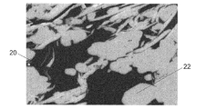
本発明の実施形態は、ある体積の画像を形成する際に取得しなければならないデータ・サンプルの数を減らす方法および該方法が組み込まれた装置を対象とする。好ましい一実施形態は、画像化された体積には一般に対象の構造体を表す特定の部分が存在し、画像データの残りの部分には価値がほとんどまたは全くないことに依拠している。例えば、図1では、細胞10が対象の構造体であり、画像中に明灰色のフィールドとして現われているエポキシ封入剤12は対象の構造体ではない。同様に、図2では、頁岩20が対象の構造体であり、白色のフィールドとして現われている間隙物質22は対象の構造体ではない。
Embodiments of the present invention are directed to a method and apparatus incorporating the method that reduces the number of data samples that must be acquired when forming a volume image. One preferred embodiment relies on the imaged volume generally having a particular portion that represents the structure of interest, and the rest of the image data having little or no value. For example, in FIG. 1, the
画素データを収集するための走査を、対象のエリアでないエリアで実行することを回避するため、あるエリアを完全に走査する前に、典型的には走査画像形成装置の一部を構成するデータ処理装置によって、どのエリアが対象の構造体を表し、どのエリアがそうでないのかについての判定を実施しなければならない。図1および2に示した2つの例では、対象の領域でない領域の方が対象の領域よりも明るい。そうであるときに、それよりも暗いグレー・シェード(gray shade)を選択するしきい値を設定し、そこまでは暗くない(リターン・レベルが十分に高い)画素を排除する方法は、対象の領域と対象の領域でない領域とを区別する1つの方法となる。 Data processing that typically forms part of a scanned image forming device before completely scanning an area to avoid performing a scan to collect pixel data in an area that is not the area of interest Depending on the device, a determination must be made as to which area represents the structure of interest and which is not. In the two examples shown in FIGS. 1 and 2, the non-target region is brighter than the target region. If so, a method of setting a threshold that selects a gray shade that is darker than that and eliminating pixels that are not so dark (with a sufficiently high return level) is This is one method for distinguishing between an area and a non-target area.
ある画素がさらなる走査に値するかどうかを判断するのに足る、グレー・シェード値の予備的な推定値を得るため、3つの技法を使用することができる。以下の段落ではそれらの3つの技法をより詳細に説明する。第1に、一連の走査を足し合わせて統合された走査を形成するシステムにおいて、第1の走査または第1の走査セットのそれぞれの画素のグレースケールをあるしきい値と比較して、上記の判断を実施することができ、次いでその判断を、この統合された走査の後続の走査に対して使用する。第2に、FIB/SEMデュアル・ビーム・システムによってある体積を画像化すると、以前に画像化した表面が、同じ対象の構造体の範囲に含まれるエリアを有することがある。例えば、生物構造体は、漸進的に露出させた多くの表面にまたがって広がっていることがある。したがって、直前の表面において対象の構造体の位置を決定し、その情報を、統合された走査の最初の走査データとともに使用して、そのときに画像化している表面内においてその対象の構造体を見つけることができる。最後に、同じ単一の走査内において、以前に走査した画素と将来に走査する画素とを相互に関係づけることができる。 Three techniques can be used to obtain a preliminary estimate of the gray shade value that is sufficient to determine if a pixel is worth further scanning. The following paragraphs describe these three techniques in more detail. First, in a system that combines a series of scans to form an integrated scan, the grayscale of each pixel of the first scan or first scan set is compared to a threshold value and A decision can be made and then used for subsequent scans of this integrated scan. Second, when a volume is imaged by the FIB / SEM dual beam system, the previously imaged surface may have areas that fall within the scope of the same object structure. For example, biological structures may extend across many progressively exposed surfaces. Thus, the position of the target structure on the previous surface is determined and that information is used along with the first scan data of the integrated scan to locate the target structure within the surface being imaged at that time. Can be found. Finally, within the same single scan, previously scanned pixels and future scanned pixels can be correlated.
前述のとおり、走査電子顕微鏡は、電子ビームを使用してある試料エリアを複数回(例えば20回)走査し、その間に、2次電子検出器によって2次電子を集めてその試料エリアの画像を形成することによって、画像を形成する。このようにするのは、電子ビームが試料上のいずれかの位置に入射しているときに、その位置に電荷が蓄積することを防ぐためである。走査ごとに、それぞれの画素のビームに対する反応性、すなわち集められた2次電子の数(すなわち真の画素グレースケール)を測定する。最初の走査で、それらの画素グレースケール測定値をあるしきい値と比較して、それらの測定値が、対象の領域でない領域からの測定値であるとはっきりとみなすことができる十分に低い値を有するかどうかを判定することができる。しかしながら、図3を参照すると、(一連の走査のうちの)単一の走査の後、(真の画素グレースケールの理論上のしきい値に正確に一致する測定値の)このような測定110はそれぞれ、かなり幅の広い誤り確率密度関数(PDF)112を有する。このことは、実際の画素グレースケールが画素グレースケール測定値よりもかなり高い可能性が相当にあることを示す。その結果、将来の走査でその画素を走査しないと誤って判断してしまうことを避けるために、控え目なしきい値114を設定することが必要となる。図4を参照すると、走査を統合することにより、統合されたそれぞれの画素測定110について、誤りPDF112の幅は狭まり、しきい値114を低くすることができ、それによってより多くの画素を将来の走査から排除することができる。走査の回数をさらに増やすと、PDFの幅は図5に示すようにさらに狭まり、最初の走査によって示された強度よりも高い強度を実際に有する画素を排除してしまう可能性をあまり高めることなく、よりぴったりしたしきい値114を使用することができる。
As described above, a scanning electron microscope uses an electron beam to scan a sample area a plurality of times (for example, 20 times), and during that time, collects secondary electrons by a secondary electron detector and displays an image of the sample area. By forming, an image is formed. This is to prevent charges from being accumulated at any position on the sample when the electron beam is incident on the position. For each scan, the reactivity of each pixel to the beam, ie, the number of secondary electrons collected (ie, true pixel gray scale) is measured. On the first scan, the pixel grayscale measurements are compared to a certain threshold value, and these measurements are sufficiently low that they can be clearly considered as measurements from areas that are not the area of interest Can be determined. However, referring to FIG. 3, after a single scan (of a series of scans) such a measurement 110 (of a measurement that exactly matches the theoretical threshold of the true pixel grayscale). Each have a fairly wide error probability density function (PDF) 112. This indicates that the actual pixel grayscale is quite likely to be much higher than the pixel grayscale measurement. As a result, it is necessary to set a
好ましい一実施形態では、所定の回数の走査を実行するまで、またはこのプロセスによって排除される追加の画素数が所定のレベルよりも少なくなるまで、このプロセスを続ける。しかしながら、画素排除の終りは必ずしも走査の終りではない。これは、対象の領域の画素グレースケールをより正確に評価するために、データを集め続けることが望ましいことがあるためである。好ましい一実施形態では、特に変化に富む走査応答を有する領域については、よりいっそう正確な画素グレースケールを形成することができるように、統合された走査の標準走査回数よりも走査回数を増やして走査する。好ましい代替実施形態では、統合された走査プロセスの最初の走査の後にだけ、画素を将来の走査から排除する。好ましい追加の代替実施形態では、閉じた形状を検出し、その形状については将来の走査に含め、閉じた形状の内側にない画素については将来の走査から排除する。 In a preferred embodiment, the process continues until a predetermined number of scans have been performed, or until the number of additional pixels eliminated by the process is below a predetermined level. However, the end of pixel exclusion is not necessarily the end of scanning. This is because it may be desirable to keep collecting data in order to more accurately evaluate the pixel grayscale of the region of interest. In a preferred embodiment, particularly for regions with a variable scan response, scans are increased more times than the standard scan number of integrated scans so that a more accurate pixel gray scale can be formed. To do. In a preferred alternative embodiment, pixels are excluded from future scans only after the first scan of the integrated scan process. In a preferred additional alternative embodiment, a closed shape is detected and included in the future scan for that shape and excluded from future scans for pixels not inside the closed shape.
集束イオン・ビーム(FIB)/走査電子顕微鏡(SEM)では、FIBが、材料の部分層を切削により除去し、SEMが、露出した表面を画像化する。最初の表面を画像化した後、その画像を、次の走査における対象の構造体の位置の予備的な指示を与えるガイドとして使用することができる。多くの試料は、規則的な形状を有し(例えば生物試料中の細胞)、画像化平面間の間隔よりも大きい、対象の構造体を含む。したがって、ある画素が、画像化された第1の平面内の対象の構造体の外側にあることは、近隣の平面内の対応する画素も対象の構造体の外側にあることを都合よく指示する。この情報は、統合された走査のうちの最初の1回または数回の走査による情報と結合されて、ある画素を後続の走査に含めるべきか否かに関する改良された指標を提供する。 In a focused ion beam (FIB) / scanning electron microscope (SEM), the FIB removes a partial layer of material by cutting, and the SEM images the exposed surface. After imaging the first surface, the image can be used as a guide that gives a preliminary indication of the position of the structure of interest in the next scan. Many samples contain structures of interest that have a regular shape (eg, cells in a biological sample) and are larger than the spacing between imaging planes. Thus, a pixel being outside the target structure in the imaged first plane conveniently indicates that the corresponding pixel in the neighboring plane is also outside the target structure. . This information is combined with information from the first one or several of the combined scans to provide an improved indication as to whether a pixel should be included in subsequent scans.
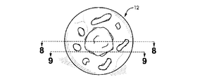
図6〜9はこの点を示しており、図6は、エポキシ中に固定された4つの酵母細胞を示し、図7は、これらの細胞のうちの左上の細胞の上面図を示し、図8および9は、図7に画定された平面8−8および9−9に沿って切った、図7の細胞の狭い間隔で離隔した2つの断面を示す。好ましい一実施形態は、図8に示した第1の画像平面からの細胞12についてのデータと図9に示した第2の画像平面からの細胞12についてのデータの間の相互関係に依拠する。これらの2つのスライスは互いに近接しているため、図から分かるように、これらのスライスは全体的に類似している。図8の断面からの画素を、次のフレーム(図9)内の近くの画素の将来の評価と相互に関係づけることによって、この類似性の利益を得ることができる。第1にすべきことは、どの画素が細胞物質12ではなく単なるエポキシを表すのかの判定を支援し、統合された走査の最初の走査以降、それらのエリアを走査することを回避することである。好ましい一実施形態では、細胞12の縁の近くの画素に対してもこの相関因子を継続する。これは、細胞の縁が、直前に走査した平面内の同様の位置にある画素の対象の領域の値(真かまたは偽か)を反映しない可能性がより高いエリアであるためである。好ましい一実施形態では、細胞の境界の内側にある画素に、次の平面における対象の領域の値について非常に高い相関値(0.85)を与え、この値を、細胞の境界から20画素分の距離に達するまで直線的に小さくする。より進んだ実施形態では、画素グレースケールを使用して、例えば両方の走査に細胞器官30が出現し、細胞器官30が概ね同じ材料であるときに、次の走査において画素グレースケールのより迅速な評価を得ることができる。
FIGS. 6-9 illustrate this point, FIG. 6 shows four yeast cells immobilized in epoxy, FIG. 7 shows a top view of the upper left cell of these cells, and FIG. And 9 show two closely spaced sections of the cells of FIG. 7 taken along planes 8-8 and 9-9 defined in FIG. One preferred embodiment relies on the interrelationship between data for
さらに、走査を始めた後、近隣の画素からの情報を、これから走査しようとしている画素に関係づけ、その情報を使用して、その画素を走査すべきかどうかを判定するためのしきい値設定の確実性を高めることができる。好ましい一実施形態では、この判断を実施するために、まっすぐなラスタ走査ではない走査を実施する。例えば、10行おきおよび10列おきに画素を走査することは、より詳細な走査を実行する前に、対象の領域がどこにあるのかを決定するのに役立つことがある。 In addition, after starting the scan, the information from neighboring pixels is related to the pixel that is about to be scanned, and that information is used to set a threshold for determining whether the pixel should be scanned. Certainty can be increased. In a preferred embodiment, a scan that is not a straight raster scan is performed to make this determination. For example, scanning pixels every 10 rows and every 10 columns may help determine where the region of interest is before performing a more detailed scan.
さらに、統合された走査プロセスのうちの最初の走査または最初の走査セットからの対象の画素の周囲のエリアの画素分散(variance)、または同じ走査内の以前に走査した画素からの対象の画素の周囲のエリアの画素分散を使用して、対象の領域の存在を判定することができる。これは、対象の領域の方が、ある体積の一様なエポキシなどの背景エリアが有するよりも多くの特徴部分を有する傾向があるためである。 Furthermore, the pixel variance of the area around the pixel of interest from the first scan or first scan set of the integrated scanning process, or of the pixel of interest from previously scanned pixels within the same scan The pixel variance of the surrounding area can be used to determine the presence of the region of interest. This is because the region of interest tends to have more features than a background area such as a certain volume of uniform epoxy.
対象の領域の方が対象の領域でない領域よりも高い値の画素を有し、より高い画素分散を有するエリアの方が、より低い画素分散を有する領域よりも対象の領域を表す可能性が高いある体積を走査する際に使用する好ましい一実施形態では、上で論じた全ての因子をひとまとめにし、以下のしきい値設定不等式を使用して、どの画素を走査すべきかを判定する。 The target area has a higher value pixel than the non-target area, and areas with higher pixel variance are more likely to represent the target area than areas with lower pixel variance In a preferred embodiment for use in scanning a volume, all the factors discussed above are combined and the following threshold setting inequality is used to determine which pixels should be scanned.
T<CR *R+CPSF *(前表面係数)+*ΣCSP(SP.Px−R)+CV *(局所画素分散)−ε (1)
上式で、
T=しきい値
CR=統合された走査の以前の走査における同じ画素に対する重みづけ定数
R=以前の走査における画素のビーム反応性の示数
CPSF=前表面係数(Provious Surface Factor)に対する重みづけ定数
前表面係数は、画素が、以前に走査した近隣の表面内の対象の領域内にある場合には=1、#ofpix<20の場合には=1/#ofpix、そのほかの場合には=0であり、#ofpixは、以前に走査した近隣の平面における対象の領域からの距離を画素数で表したものである。
T <C R * R + C PSF * (front surface coefficient) + * ΣC SP (SP.Px−R) + C V * (local pixel variance) −ε (1)
Where
T = threshold C R = weighting constant for the same pixel in the previous scan of the merged scan R = indication of the beam reactivity of the pixel in the previous scan C PSF = weight for the front surface factor (Provious Surface Factor) Bending constant The front surface coefficient is = 1 if the pixel is in the region of interest in the previously scanned neighboring surface, = 1 / # ofpix if #ofpix <20, otherwise = 0, and #ofpix represents the distance from the target region in the previously scanned neighboring plane in terms of the number of pixels.
CSP=既に走査した同じ走査、同じ平面の相互に関係づけられたそれぞれの画素に対する重みづけ定数
SP.Px=既に走査した同じ平面の相互に関係づけられた画素
CV=局所画素分散に対する重みづけ定数
局所画素分散(Regionl Pixel Variance)=対象の画素の周囲のある画定されたエリア内、例えば100×100画素のエリア内の画素の分散
ε=ある画素を対象の画素ではないと誤って分類する所定の誤り率を与えるように設定された誤りマージン
さらに、好ましい一実施形態では、画素に対する測定誤差があるしきい値よりも低いときには、たとえ対象の構造体に対するものであっても、それぞれの画素のさらなる走査を停止する。すなわち、以前の表面からの情報、統合された走査の以前の走査からの情報および同じ平面内の以前に走査した画素からの情報を考慮することによって、その画素の値が所定の許容値よりも小さいと判定されたことをシステムが確信することができるときには、その画素を再び走査することはしない。
C SP = weighting constant SP. For the same scan already scanned, each interrelated pixel in the same plane. Px = interrelated pixels in the same plane that have already been scanned C V = weighting constant for local pixel variance Local Pixel Variance = within a defined area around the pixel of interest, eg 100 × Dispersion of pixels within an area of 100 pixels ε = error margin set to give a predetermined error rate that erroneously classifies a pixel as not a pixel of interest Further, in a preferred embodiment, the measurement error for a pixel is When below a certain threshold, further scanning of each pixel is stopped, even for the target structure. That is, by taking into account information from previous surfaces, information from previous scans of integrated scans, and information from previously scanned pixels in the same plane, the value of that pixel is greater than a predetermined tolerance When the system can be sure that it is determined to be small, it does not scan the pixel again.
状況によっては、式(1)の情報の一部が使用できないことがある。例えば、統合された走査を使用しない場合には最初の項「R」を得ることができず、どの画素の走査を回避するのかについての判定は、以前に走査した表面との相互関係または相互に関係づけられた同じ平面内の既に走査した画素との相互関係だけに基づいて実施しなければならない。画像形成の所要時間は体積画像化だけの問題ではなく、モザイク画像化にも関連する。例えば、モザイク画像の形成では、1ギガバイト以上の画素を集める必要があることがある。この場合、走査すべきでないエリアの判定に、以前の平面からの情報は使用できず、統合された走査からのデータおよび同じ走査からのデータだけが使用可能である。最後に、同じ走査であっても、走査したばかりの画素を遅れずに十分に評価して、次に走査する予定の画素を走査すべきか否かついての判断を下すことができないことがありうる。これらの場合にはそれぞれ、式1から1つの項を除き、εを大きくして、対象の画素を走査しないと誤って判断してしまわないようにする。 Depending on the situation, some of the information in equation (1) may not be available. For example, if the integrated scan is not used, the first term “R” cannot be obtained, and the determination of which pixel to avoid scanning is related to or relative to the previously scanned surface. It must be done based solely on the correlation with the already scanned pixels in the same related plane. The time required for image formation is related not only to volume imaging but also to mosaic imaging. For example, in forming a mosaic image, it may be necessary to collect 1 gigabyte or more of pixels. In this case, information from previous planes cannot be used to determine areas that should not be scanned, only data from the integrated scan and data from the same scan can be used. Finally, even with the same scan, it may not be possible to make a thorough evaluation of the pixel that has just been scanned without delay and to decide whether or not to scan the next pixel to be scanned. . In each of these cases, except for one term from Equation 1, ε is increased so that it is not erroneously determined that the target pixel is not scanned.
好ましい一実施形態では、CR、CPSF、CSP、CVおよびが、ユーザが入力することができる画像化する材料のタイプおよび内部特徴部分の方向に従って設定される。例えば、画像平面を貫いて走る多くの長い特徴部分を有する材料を画像化する場合には、CPSFを比較的に高く設定し、εを比較的に低く設定する。ユーザは、(必要に応じて)材料のタイプおよび内部特徴部分の方向を、ユーザ・インタフェース、例えばドロップ・ダウン・メニューによって入力することができる。このドロップ・ダウン・メニューは例えば組織のタイプ、コア試料のタイプなどのリストを示す。別のドロップ・ダウン・メニューは方向の選択を可能にする。 In a preferred embodiment, C R , C PSF , C SP , C V and are set according to the type of material to be imaged and the direction of internal features that the user can enter. For example, when imaging a material with many long features running through the image plane, CPSF is set relatively high and ε is set relatively low. The user can enter the type of material (if necessary) and the orientation of the internal features via a user interface, eg, a drop down menu. This drop down menu shows a list of tissue types, core sample types, etc., for example. Another drop down menu allows selection of direction.
前述のとおり、好ましい一実施形態では、統合された走査の初期の走査、以前の表面からの情報および/または同じ走査からの情報を使用して、対象の構造体(例えば細胞)の境界を検出する。境界内のエリアはさらに走査し、境界の外側のエリアは走査しない。 As described above, in a preferred embodiment, the initial scan of the integrated scan, information from previous surfaces and / or information from the same scan is used to detect the boundaries of the structure of interest (eg, a cell). To do. The area within the boundary is further scanned, and the area outside the boundary is not scanned.
図10は、本発明の好ましい実施形態を実現する目的に使用することができる典型的なデュアル・ビームFIB/SEMシステム1010を示す。デュアル・ビーム・システムを参照するが、本発明の態様はデュアル・ビーム・システムだけに限定されず、単一ビーム・システムなどの他の荷電粒子ビーム・システムで実現することもできる。本発明の一実施形態は、試料表面の平面に対して垂直なまたは試料表面の平面に対して数度傾いたイオン・ビームと、イオン・ビームの軸から例えば52度傾いた軸を有する電子ビームとを使用するデュアル・ビームFIB/SEMシステム1010を利用する。いくつかの実施形態では、イオン・ビームの視野と電子ビームの視野が互いから数ミクロン以内に位置するように、これらの両方のビームが互いに整列することができる。イオン・ビームは一般に加工物を画像化する目的および加工する目的に使用され、電子ビームは主に画像を形成する目的に使用されるが、加工物を改変する目的に電子ビームを使用することもできる。電子ビームは一般に、イオン・ビーム画像よりも高分解能の画像を生成し、イオン・ビームとは違い、入射した表面を傷つけない。これらの2つのビームによって形成される画像は異なって見えることがあり、したがってこれらの2つのビームは、単一のビームよりも多くの情報を提供することができる。
FIG. 10 illustrates an exemplary dual beam FIB /
このようなデュアル・ビーム・システムは、別個の構成要素から製作することができ、あるいはFEI Company(米オレゴン州Hillsboro)から販売されているAltura(商標)またはExpida(商標)システムなどの従来の装置を基にして構成することもできる。本発明は、例えばFIBだけのシステム、SEMだけのシステムなどの単一ビーム・システム、または2つのFIBカラムを有するデュアル・ビーム・システムを含む、他の粒子ビーム・システムを使用して実現することもできる。 Such dual beam systems can be made from separate components or conventional devices such as Altura ™ or Expida ™ systems sold by FEI Company (Hillsboro, Oreg.). It can also be configured on the basis of The present invention is implemented using other particle beam systems, including single beam systems such as FIB only systems, SEM only systems, or dual beam systems with two FIB columns, for example. You can also.
集束イオン・ビーム・システム1010は、上部ネック部分1012を有する排気された囲い1011を含み、上部ネック部分1012内にはイオン源1014および集束カラム1016が位置し、集束カラム1016は、引出し電極および静電光学系を含む。イオン源1014を出たイオン・ビーム1018は、カラム1016を通過し、1020に概略的に示されている静電偏向手段間を通り抜けて、下室1026内の可動X−Y−Zステージ1024上に配置された試料1022に向かって進む。イオン・ポンプまたは他のポンピング・システム(図示せず)を使用してネック部分1012を排気することができる。室1026は、真空コントローラ1032の制御の下、ターボ分子および機械ポンピング・システム1030によって排気される。この真空システムは、室1026に、約1×10⁻⁷トルから5×10⁻⁴トルの間の真空を提供する。エッチング支援ガス、エッチング遅延ガスまたは付着前駆体ガスを使用する場合、室のバックグラウンド圧力は典型的には約1×10⁻⁵トルまで上昇することがある。
The focused
イオン源1014と、イオン・ビーム1018を形成し下方へ導く集束カラム1016内の適当な電極とに高圧電源1034が接続される。パターン発生器1038によって提供される所定のパターンに従って動作する偏向コントローラおよび増幅器1036が偏向板1020に結合され、それによって対応するパターンを試料1022の上面に描くようにビーム1018を制御することができる。いくつかのシステムでは、当技術分野ではよく知られているように、偏向板が、最後のレンズの前に配置される。
A high
イオン源1014は一般にガリウムの金属イオン・ビームを提供するが、マルチカスプ(multicusp)イオン源、他のプラズマ・イオン源など、他のイオン源を使用することもできる。イオン・ミリング、強化されたエッチングもしくは材料付着によって試料1022を改変するため、または試料1022を画像化するために、イオン源1014を一般に、試料1022の位置における幅が1/10ミクロン未満のビームに集束させることができる。画像化のために2次イオンまたは2次電子の放出を検出する目的に使用される荷電粒子増倍器1040が信号処理装置1042に接続されており、荷電粒子増倍器1040からの信号は信号処理装置1042で増幅され、ディジタル信号に変換され、信号処理にかけられる。その結果生成されるディジタル信号は、試料1022の画像をモニタ1044に表示する。
The
FIB/SEMシステム1010はさらに、走査電子顕微鏡1041と電源および制御ユニット1045を備える。陰極1052と陽極1054の間に電圧を印加することによって、陰極1052から電子ビーム1043が放出される。電子ビーム1043は、集光レンズ1056および対物レンズ1058によって微細なスポットに集束する。電子ビーム1043は、偏向コイル1060によって試料の表面を2次元的に走査する。集光レンズ1056、対物レンズ1058および偏向コイル1060の動作は電源および制御ユニット1045によって制御される。
The FIB /
電子ビーム1043を、下室1026内の可動X−Y−Zステージ1024上にある試料1022の表面に集束させることができる。走査電子顕微鏡1041は、微細な集束電子ビーム1043を生成し、微細な集束電子ビーム1043は構造体の表面にわたって、好ましくはあるラスタ・パターンに従って走査する。電子ビーム1043中の電子が加工物1022の表面に衝突すると、2次電子および後方散乱電子が放出される。この2次電子および後方散乱電子はそれぞれ、2次電子検出器1040または後方散乱電子検出器1062によって検出される。2次電子検出器1140または後方散乱電子検出器1062によって生成されたアナログ信号は、信号処理ユニット1042によって増幅され、ディジタル輝度値に変換される。その結果生成されるディジタル信号を、試料1022の画像としてモニタ1044に表示することができる。
The
ステージ1024上に試料1022を挿入するため、および内部ガス供給リザーバが使用される場合には内部ガス供給リザーバを使用可能とするために、扉1070が開かれる。ステージ1024は加熱または冷却されていることがある。システムが真空状態にある場合に開かないように、この扉はインタロックされる。イオン・ビーム1018にエネルギーを与え集束させるため、高電圧電源は、イオン・ビーム・カラム1016内の電極に適当な加速電圧を印加する。
ガス蒸気を導入し試料1122に向かって導くためにガス送達システム1046が下室1026内へ延びている。本発明の譲受人に譲渡されたCasella他の「Gas Delivery Systems for Particle Beam Processing」という名称の米国特許第5,851,413号は適当なガス送達システム1046を記載している。別のガス送達システムが、やはり本発明の譲受人に譲渡されたRasmussenの「Gas Injection System」という名称の米国特許第5,435,850号に記載されている。例えば、ヨウ素を送達してエッチングを強化することができ、または金属有機化合物を送達して金属を付着させることができる。
A
システム・コントローラ1019は、デュアル・ビーム・システム1010のさまざまな部分の動作を制御する。従来のユーザ・インタフェース(図示せず)にコマンドを入力することによって、ユーザは、システム・コントローラ1019を介してイオン・ビーム1018または電子ビーム1043を思い通りに走査することができる。システム・コントローラ1019は、コンピュータ可読の記憶装置1021をさらに備えることができ、記憶装置1021に記憶されたデータまたはプログラムされた命令に従ってデュアル・ビーム・システム1010を制御することができる。試料に関するCADデータまたは記憶装置1021に記憶されたCADデータを使用して、前述のように対象の特徴部分および位置合せ点または転写基準点の位置を決定する目的に使用されるCAD多角形オーバレイまたは他の位置データを生み出すことができる。
The
本発明のいくつかの実施形態によれば、あるエリアのディジタル画像を走査顕微鏡を使用して迅速に形成する方法は、試料のそのエリアを繰り返し走査するステップと、それらの複数の走査によるそれぞれの画素の検出器信号を統合して、そのエリアの画像を生成するステップとを含み、これらのステップは、最初の走査または最初の走査セットを実行して、前記エリアに対するガイド画素セットを形成するステップであり、このガイド画素セットが、最初の走査または最初の走査セットの画素のサブセットであり、最初の走査または最初の走査セットの画素のグレー・レベルに基づいて選択されるステップと、前記ガイド画素セットを使用して、前記エリア内の対象の構造体を表す領域を識別するステップと、前記領域内の画素をさらに評価するために、対象の構造体を表す前記領域の追加の走査を実行して追加のデータを集め、そのエリア内の他の領域は走査しないステップとを含む。 According to some embodiments of the present invention, a method for rapidly forming a digital image of an area using a scanning microscope comprises the steps of repeatedly scanning that area of the sample and each of those multiple scans. Integrating the detector signals of the pixels to generate an image of the area, these steps performing an initial scan or an initial scan set to form a guide pixel set for the area The guide pixel set is a first scan or a subset of pixels of the first scan set and is selected based on a gray level of pixels of the first scan or first scan set; Using the set to identify a region representing the structure of interest within the area; and further evaluating the pixels within the region. To, to perform additional scanning of the region representing the structure of interest collect additional data, other areas within the area and a step which is not scanned.
いくつかの実施形態では、前記走査または走査セットが単一の走査だけを含む。いくつかの実施形態では、前記最初の走査または最初の走査セットが、対象の構造体を取得するように適合された走査パターンに従った前記エリアの部分走査を含む。いくつかの実施形態では、前記エリアが、材料を漸進的に除去して新たな表面を露出させ、新たな表面が露出するたびに前記新たな表面を走査することによって走査している体積の一部分であり、前記最初の走査または最初の走査セットが、前記体積内の以前に露出させた表面の走査を含む。 In some embodiments, the scan or scan set includes only a single scan. In some embodiments, the initial scan or initial scan set includes a partial scan of the area according to a scan pattern adapted to obtain a structure of interest. In some embodiments, the area is a portion of the volume being scanned by progressively removing material to expose a new surface and scanning the new surface each time a new surface is exposed. And the first scan or first scan set includes a scan of a previously exposed surface within the volume.
いくつかの実施形態では、対象の領域が、少なくとも部分的には、画素強度を評価することによって識別される。いくつかの実施形態では、対象の領域が、部分的には、局所画素分散を評価することによって識別される。 In some embodiments, the region of interest is identified, at least in part, by evaluating pixel intensity. In some embodiments, the region of interest is identified, in part, by evaluating local pixel variance.
あるエリアの走査を実行するように適合された走査顕微鏡アセンブリは、前記エリアの前記走査を実行する部分として、荷電粒子源と、荷電粒子ビームで加工物を走査する偏向器と、荷電粒子ビームを加工物の表面に集束させるレンズと、荷電粒子ビームの衝突に反応した加工物からの放出を検出する検出器と、走査荷電粒子ビーム・アセンブリの動作を制御するコンピュータと、コンピュータ可読記憶装置とを備え、このコンピュータ可読記憶装置は、最初の走査または最初の走査セットを実行して、前記エリアに対するガイド画素セットを形成するステップであり、このガイド画素セットが、最初の走査または最初の走査セットの画素のサブセットであり、最初の走査または最初の走査セットの画素のグレー・レベルに基づいて選択されるステップと、前記ガイド画素セットを使用して、前記エリア内の対象の構造体を表す領域を識別するステップと、前記領域内の画素をさらに評価するために、対象の構造体を表す前記領域の追加の走査を実行して追加のデータを集め、そのエリア内の他の領域は走査しないステップとを実行するための命令を記憶している。 A scanning microscope assembly adapted to perform a scan of an area includes a charged particle source, a deflector that scans a workpiece with a charged particle beam, and a charged particle beam as the portion that performs the scan of the area. A lens for focusing on the surface of the workpiece; a detector for detecting emission from the workpiece in response to the impact of the charged particle beam; a computer for controlling the operation of the scanning charged particle beam assembly; and a computer readable storage device. The computer-readable storage device is configured to perform a first scan or a first scan set to form a guide pixel set for the area, the guide pixel set being the first scan or the first scan set. A subset of pixels, selected based on the gray level of the pixels in the first scan or first scan set Identifying a region representing the target structure within the area using the guide pixel set; and further evaluating the pixels representing the target structure for further evaluation of pixels within the region. Instructions are stored to perform additional scans to collect additional data and perform other steps in the area that do not scan.
いくつかの実施形態では、前記最初の走査または最初の走査セットが単一の走査だけを含む。いくつかの実施形態では、前記最初の走査または最初の走査セットが、対象の構造体を取得するように適合された走査パターンに従った前記エリアの部分走査である。 In some embodiments, the first scan or first scan set includes only a single scan. In some embodiments, the initial scan or initial scan set is a partial scan of the area according to a scan pattern adapted to obtain a structure of interest.
いくつかの実施形態では、前記エリアが、材料を漸進的に除去して新たな表面を露出させ、新たな表面が露出するたびに前記新たな表面を走査することによって走査している体積の一部分であり、前記最初の走査または最初の走査セットが、前記体積内の以前に露出させた表面の走査を含む。いくつかの実施形態では、対象の領域が、少なくとも部分的には、画素強度を評価することによって識別される。いくつかの実施形態では、対象の領域が、少なくとも部分的には、局所画素分散を評価することによって識別される。 In some embodiments, the area is a portion of the volume being scanned by progressively removing material to expose a new surface and scanning the new surface each time a new surface is exposed. And the first scan or first scan set includes a scan of a previously exposed surface within the volume. In some embodiments, the region of interest is identified, at least in part, by evaluating pixel intensity. In some embodiments, the region of interest is identified, at least in part, by evaluating local pixel variance.
本発明のいくつかの実施形態によれば、対象の領域と対象の領域でない領域とを含むあるエリアの画像を走査画像化装置を使用して形成する方法は、短時間の走査を実行し、それにより、可能な正確さよりも劣る正確さを有する情報を、より短い時間で集めるステップと、前記短時間の走査によるデータを使用して、対象の領域でない領域を表す画素を決定するステップと、より低速で走査を実行するが、対象の領域でない領域を表すと判定された画素は走査せず、それによって前記走査をより速やかに完了させるステップとを含む。 According to some embodiments of the present invention, a method of forming an image of an area including a region of interest and a region that is not a region of interest using a scanning imaging device performs a short scan, Thereby collecting information having an accuracy less than possible with a shorter time, and using the data from the short scan to determine a pixel representing a region that is not a region of interest; Performing a scan at a slower rate, but not scanning pixels determined to represent non-target regions, thereby completing the scan more quickly.
いくつかの実施形態では、前記走査装置が走査電子顕微鏡である。いくつかの実施形態では、前記エリアが、1つに組み合わされて組み合わされた画像を形成する一組のエリアのうちの1つのエリアである。いくつかの実施形態では、前記エリアが、その平面次元に対して垂直に積み重なってある体積を形成する一組のエリアのうちの1つのエリアである。いくつかの実施形態では、前記エリアが、モザイク状に集合した一組のエリアのうちの1つのエリアである。 In some embodiments, the scanning device is a scanning electron microscope. In some embodiments, the area is one area of a set of areas that are combined together to form a combined image. In some embodiments, the area is one of a set of areas forming a volume that is stacked perpendicular to its planar dimension. In some embodiments, the area is one of a set of areas assembled in a mosaic pattern.
いくつかの実施形態では、前記短時間の走査が、統合された走査プロセス中に実行される第1の走査セットである。いくつかの実施形態では、前記第1の走査セットが単一の走査だけを含む。 In some embodiments, the short scan is a first scan set that is performed during an integrated scanning process. In some embodiments, the first scan set includes only a single scan.
本発明のいくつかの実施形態によれば、走査電子顕微鏡アセンブリは、走査する試料中の対象の構造体の寸法特性をユーザが入力することを可能にするように適合されたデータ入力サブアセンブリを含み、前記寸法特性が前記試料の走査に影響を及ぼす。 According to some embodiments of the present invention, a scanning electron microscope assembly includes a data input subassembly adapted to allow a user to input dimensional characteristics of a structure of interest in a sample to be scanned. And the dimensional characteristics affect the scanning of the sample.
いくつかの実施形態では、前記寸法特性が、走査のどの部分が対象の領域でない領域であり、スキップすべきなのかを判定するアルゴリズムに影響を及ぼす。いくつかの実施形態では、前記データ入力サブアセンブリがドロップ・ダウン・メニューを含む。本発明のいくつかの実施形態によれば、走査顕微鏡を使用して試料の画像を迅速に形成する方法は、画素の第1のセットからなる第1のエリアの最初の走査または最初の走査セットを実行して、第1のセット中のそれぞれの画素の第1のグレー・レベル値を決定するステップと、第1のセット中の画素の第1のグレー・レベルを解析して、前記エリア内の対象の構造体を表す第1の領域を識別するステップであり、この第1の領域が、第1のセットの画素数よりも少ない数の画素を含むステップと、前記領域の追加の走査を実行して、前記領域の画素についてのみ第2のグレー・レベル値を決定するステップであり、第2のグレー・レベル値が、第1のグレー・レベルを決定するのに使用した走査の回数よりも多くの回数の走査を統合することによって決定され、それによって、前記領域内の画素のグレー・レベル測定値の正確さを向上させ、一方で、前記追加の走査に含める画素を減らすステップとを含む。 In some embodiments, the dimensional characteristics affect an algorithm that determines which portions of the scan are areas that are not areas of interest and should be skipped. In some embodiments, the data entry subassembly includes a drop down menu. According to some embodiments of the present invention, a method for rapidly forming an image of a sample using a scanning microscope includes a first scan of a first area consisting of a first set of pixels or an initial scan set. To determine a first gray level value for each pixel in the first set; and analyzing the first gray level of the pixels in the first set to Identifying a first region representing a target structure of the first set, wherein the first region includes a number of pixels less than the number of pixels of the first set; and additional scanning of the region And determining a second gray level value for only the pixels of the region, wherein the second gray level value is greater than the number of scans used to determine the first gray level. Also integrate many scans It is determined by, thereby improving the accuracy of the gray level measurement values of the pixels in the area, on the one hand, and a step of reducing the pixel to be included in the additional scan.
いくつかの実施形態では、第1のセット中の画素の第1のグレー・レベルを解析して第1の領域を識別するステップが、画素の第1のグレー・レベルをしきい値と比較するステップを含み、このしきい値が、画素の第1のグレー・レベルを決定するのに使用した統合された走査の回数に依存する。いくつかの実施形態では、第1のセット中の画素の第1のグレー・レベルを解析して第1の領域を識別するステップが、画素の第1のグレー・レベルをしきい値と比較するステップを含み、このしきい値が、隣接する画素のグレー・レベルに依存する。 In some embodiments, analyzing the first gray level of the pixels in the first set to identify the first region compares the first gray level of the pixel to a threshold value. Including a step, and this threshold depends on the number of integrated scans used to determine the first gray level of the pixel. In some embodiments, analyzing the first gray level of the pixels in the first set to identify the first region compares the first gray level of the pixel to a threshold value. Step, this threshold depends on the gray level of the neighboring pixels.
いくつかの実施形態では、追加の走査を実行するステップが、第2のセット中の画素の第2のグレー・レベルを解析して、前記エリア内の対象の構造体を表す第2の領域を識別するステップを含み、前記第2の領域が、第1のセットのサブセットであり、第1のセットよりも少ない数の画素を含み、追加の走査を実行するステップがさらに、前記領域の追加の走査を実行して、前記第2の領域の画素についてのみ第3のグレー・レベル値を決定するステップを含み、この第3のグレー・レベル値が、第2のグレー・レベルを決定するのに使用した走査の回数よりも多い回数の走査を統合することによって決定される。 In some embodiments, performing the additional scan comprises analyzing a second gray level of pixels in the second set to determine a second region representing the structure of interest in the area. Identifying, wherein the second region is a subset of the first set, includes fewer pixels than the first set, and performing an additional scan further includes Performing a scan to determine a third gray level value only for pixels in the second region, the third gray level value determining the second gray level. Determined by consolidating more scans than used.
いくつかの実施形態では、この方法が、第1のエリアを含む材料の層を試料から除去することによって第2のエリアを露出させるステップと、第2のエリアの第2の領域を走査するステップであり、この第2の領域が、第2のエリア内の画素のサブセットを含み、第1の領域によって決定されるステップとをさらに含む。 In some embodiments, the method exposes the second area by removing the layer of material comprising the first area from the sample, and scanning the second region of the second area. And the second region includes a subset of pixels in the second area and is further determined by the first region.
いくつかの実施形態では、この方法が、材料を漸進的に除去して新たな表面を露出させるステップと、新たな表面が露出するたびに、それぞれの新たな表面の限定された領域を走査するステップであり、この限定された領域が、以前の走査における画素のグレー・レベルによって決定されるステップとをさらに含む。いくつかの実施形態では、前記しきい値が、近隣の画素のグレー・レベルおよび以前の層の同じ位置の画素のグレー・レベルによって決定される。 In some embodiments, the method progressively removes material to expose new surfaces and scans a limited area of each new surface each time a new surface is exposed. And wherein the limited area is determined by the gray level of the pixel in the previous scan. In some embodiments, the threshold is determined by the gray level of neighboring pixels and the gray level of pixels at the same location in the previous layer.
本発明のいくつかの実施形態によれば、走査荷電粒子ビーム・アセンブリは、荷電粒子源と、荷電粒子ビームで試料を走査する偏向器と、荷電粒子ビームを試料の表面に集束させるレンズと、荷電粒子の衝突に反応した試料からの放出を検出する検出器と、走査荷電粒子ビーム・アセンブリの動作を制御するコンピュータと、上記方法の実施形態を実行するための命令を記憶したコンピュータ可読記憶装置とを備える。 According to some embodiments of the present invention, a scanning charged particle beam assembly includes a charged particle source, a deflector that scans the sample with the charged particle beam, a lens that focuses the charged particle beam onto the surface of the sample, A detector for detecting emission from a sample in response to a charged particle impact, a computer for controlling the operation of the scanning charged particle beam assembly, and a computer readable storage device storing instructions for performing the method embodiments. With.
本発明のいくつかの実施形態によれば、走査ビームを使用して画像を形成する方法は、ある視野を走査して、その視野の中の画素値を決定するステップと、この画素値を解析して、対象の特徴部分を表す画素のサブセットを決定するステップと、この画素のサブセットだけに対して追加の走査を実行して、対象の特徴部分の画像を生成するステップとを含む。 According to some embodiments of the present invention, a method of forming an image using a scanning beam includes scanning a field of view to determine a pixel value in the field of view, and analyzing the pixel value. Determining a subset of pixels representing the feature of interest, and performing additional scanning only on the subset of pixels to generate an image of the feature of interest.
いくつかの実施形態では、画素を解析するステップが、画素のグレー・レベルをしきい値と比較するステップを含む。いくつかの実施形態では、このしきい値が、画素値を決定するのに使用した走査の回数に依存する。いくつかの実施形態では、このしきい値が、隣接する画素のグレー・レベルに依存する。いくつかの実施形態では、追加の走査を実行するステップが、材料の層を除去するステップと、新たに露出した表面を走査するステップであり、この新たに露出した表面の走査される画素が、直前の表面の対応する画素のグレー・レベルによって決定されるステップとを含む。いくつかの実施形態では、材料の層を除去するステップと、新たに露出した表面を走査するステップであり、この新たに露出した表面の走査される画素が、直前の表面の対応する画素のグレー・レベルによって決定されるステップとを繰り返して、3次元画像を形成する。 In some embodiments, analyzing the pixel includes comparing the gray level of the pixel to a threshold value. In some embodiments, this threshold depends on the number of scans used to determine the pixel value. In some embodiments, this threshold depends on the gray level of adjacent pixels. In some embodiments, performing the additional scan is removing a layer of material and scanning the newly exposed surface, where the scanned pixel of the newly exposed surface is Determined by the gray level of the corresponding pixel on the previous surface. In some embodiments, removing the layer of material and scanning the newly exposed surface, the scanned pixel of the newly exposed surface is the gray level of the corresponding pixel on the previous surface. Repeat the steps determined by the level to form a 3D image.
本発明および本発明の利点を詳細に説明したが、添付の特許請求の範囲によって定義された本発明の趣旨および範囲から逸脱することなく、本明細書に、さまざまな変更、置換および改変を加えることができることを理解すべきである。さらに、本出願の範囲が、本明細書に記載されたプロセス、機械、製造、組成物、手段、方法およびステップの特定の実施形態に限定されることは意図されていない。当業者なら本発明の開示から容易に理解するように、本明細書に記載された対応する実施形態と実質的に同じ機能を実行し、または実質的に同じ結果を達成する既存のまたは今後開発されるプロセス、機械、製造、組成物、手段、方法またはステップを、本発明に従って利用することができる。したがって、添付の特許請求の範囲は、その範囲内に、このようなプロセス、機械、製造、組成物、手段、方法またはステップを含むことが意図されている。 Having described the invention and the advantages of the invention in detail, various changes, substitutions and modifications can be made to the specification without departing from the spirit and scope of the invention as defined by the appended claims. It should be understood that it can. Furthermore, it is not intended that the scope of the application be limited to the specific embodiments of the processes, machines, manufacture, compositions, means, methods, and steps described herein. Those skilled in the art will readily understand from the present disclosure that existing or future developments that perform substantially the same function or achieve substantially the same results as the corresponding embodiments described herein. Any process, machine, manufacture, composition, means, method or step that can be utilized can be utilized in accordance with the present invention. Accordingly, the appended claims are intended to include within their scope such processes, machines, manufacture, compositions of matter, means, methods, or steps.
1010 デュアル・ビームFIB/SEMシステム
1014 イオン源
1016 集束カラム
1018 イオン・ビーム
1019 システム・コントローラ
1021 記憶装置
1022 試料
1024 可動X−Y−Zステージ
1010 Dual Beam FIB /
Claims (7)
前記試料の第1のエリアの最初の走査または最初の走査セットを実行して、前記第1のエリアに対応する一組の画素のそれぞれの画素の第1のグレー・レベル値を決定するステップと、
前記第1のグレー・レベル値を解析して、前記対象の構造体を表す前記第1のエリア内の第1の領域に対応する前記画素のサブセットを識別するステップと、
前記第1の領域に対応する前記画素のサブセットの画素についてのみ第2のグレー・レベル値を決定するために前記第1の領域の追加の走査を実行することによって、前記第1の領域に対応する画素のグレー・レベル測定値をより正確に決定するステップであり、前記第2のグレー・レベル値が、前記第1のグレー・レベル値を決定するのに使用した走査の回数よりも多くの回数の走査を統合することによって決定され、前記追加の走査は、前記最初の走査または最初の走査セットで収集された画素数よりも少ない画素についてグレー・レベルのデータを集める、ステップと
を含む方法。 A method for quickly forming an image of a structure of interest in a sample using a scanning microscope, comprising:
Determining a first running scan or first scan set, the first gray level value of each pixel of the set of pixels corresponding to the first area of the first area of the sample ,
Analyzing the first gray level value to identify a subset of the pixels corresponding to a first region in the first area representing the structure of interest ;
Corresponding to the first region by performing an additional scan of the first region to determine a second gray level value only for pixels of the subset of pixels corresponding to the first region More accurately determining a gray level measurement of the pixel to be applied, wherein the second gray level value is greater than the number of scans used to determine the first gray level value. Collecting the gray level data for pixels less than the number of pixels collected in the first scan or first scan set , wherein the additional scan is determined by integrating a number of scans. .
前記第1の領域に対応する画素のグレー・レベル測定値をより正確に決定するステップが、前記第2のグレー・レベルを複数の第2のしきい値と比較するステップを含み、複数の前記第2のしきい値が、前記追加の走査から除外する複数の画素を選択するのに用いられる、請求項1に記載の方法。 Identifying the subset of pixels corresponding to the first region comprises comparing the first gray level value to a first threshold, wherein the first threshold is the Depends on the number of scans used to determine the first gray level value;
More accurately determining a gray level measurement of a pixel corresponding to the first region comprises comparing the second gray level to a plurality of second thresholds, The method of claim 1, wherein a second threshold is used to select a plurality of pixels to exclude from the additional scan.
前記第2のエリアの第2の領域を走査するステップであり、前記第2のエリアの第2の領域が、前記第2のエリア内において前記第1の領域に対応するステップと
をさらに含む、請求項1から4のいずれかに一項に記載の方法。 Exposing a second area by removing a layer of material comprising the first area from the sample;
Scanning a second area of the second area , wherein the second area of the second area corresponds to the first area in the second area ; 5. A method according to any one of claims 1 to 4.
新たなエリアが露出するたびに、それぞれの新たなエリアの限定された領域を走査するステップであり、前記限定された領域が、以前のエリア内の対応する領域に対応する複数の画素のグレー・レベル値を解析することによって決定されるステップと
をさらに含む、請求項5に記載の方法。 Progressively removing material to expose new areas;
Each time a new area is exposed, scanning a limited area of each new area, wherein the limited area includes a plurality of pixel gray levels corresponding to corresponding areas in the previous area. The method of claim 5, further comprising: determining by analyzing the level value .
荷電粒子源と、
荷電粒子ビームで試料を走査する偏向器と、
前記荷電粒子ビームを前記試料の表面に集束させるレンズと、
前記荷電粒子の衝突に反応した前記試料からの放出を検出する検出器と、
前記走査荷電粒子ビーム・システムの動作を制御するコンピュータと、
請求項1に記載の方法を実行するための命令を記憶したコンピュータ可読記憶装置と
を備える走査荷電粒子ビーム・システム。 A scanning charged particle beam system,
A charged particle source;
A deflector that scans the sample with a charged particle beam;
A lens for focusing the charged particle beam on the surface of the sample;
A detector for detecting emission from the sample in response to the collision of the charged particles;
A computer for controlling the operation of the scanning charged particle beam system;
A scanning charged particle beam system comprising: a computer readable storage device storing instructions for performing the method of claim 1.
Applications Claiming Priority (2)
| Application Number | Priority Date | Filing Date | Title |
|---|---|---|---|
| US13/474,176 US9041793B2 (en) | 2012-05-17 | 2012-05-17 | Scanning microscope having an adaptive scan |
| US13/474,176 | 2012-05-17 |
Publications (3)
| Publication Number | Publication Date |
|---|---|
| JP2013243128A JP2013243128A (en) | 2013-12-05 |
| JP2013243128A5 JP2013243128A5 (en) | 2016-06-23 |
| JP6479303B2 true JP6479303B2 (en) | 2019-03-06 |
Family
ID=48366268
Family Applications (1)
| Application Number | Title | Priority Date | Filing Date |
|---|---|---|---|
| JP2013097243A Active JP6479303B2 (en) | 2012-05-17 | 2013-05-07 | Scanning microscope with adaptive scanning |
Country Status (4)
| Country | Link |
|---|---|
| US (1) | US9041793B2 (en) |
| EP (1) | EP2665083A3 (en) |
| JP (1) | JP6479303B2 (en) |
| CN (1) | CN103424419B (en) |
Families Citing this family (12)
| Publication number | Priority date | Publication date | Assignee | Title |
|---|---|---|---|---|
| DE102007045897A1 (en) * | 2007-09-26 | 2009-04-09 | Carl Zeiss Microimaging Gmbh | Method for the microscopic three-dimensional imaging of a sample |
| US20150144806A1 (en) * | 2012-05-29 | 2015-05-28 | Macquarie University | Two-directional scanning for luminescence microscopy |
| EP2879156A1 (en) * | 2013-12-02 | 2015-06-03 | Fei Company | Charged-particle microscopy with enhanced electron detection |
| US9502211B1 (en) * | 2015-05-03 | 2016-11-22 | Fei Company | Adaptive scanning for particle size using directed beam signal analysis |
| US10535131B2 (en) * | 2015-11-18 | 2020-01-14 | Kla-Tencor Corporation | Systems and methods for region-adaptive defect detection |
| JP6522535B2 (en) * | 2016-02-29 | 2019-05-29 | 富士フイルム株式会社 | Cell observation apparatus and method |
| US11506877B2 (en) | 2016-11-10 | 2022-11-22 | The Trustees Of Columbia University In The City Of New York | Imaging instrument having objective axis and light sheet or light beam projector axis intersecting at less than 90 degrees |
| EP3697592A4 (en) * | 2017-10-16 | 2021-05-19 | Hewlett-Packard Development Company, L.P. | 3d printer |
| EP3598474A1 (en) * | 2018-07-19 | 2020-01-22 | FEI Company | Adaptive specimen image acquisition using an artificial neural network |
| US20200118786A1 (en) * | 2018-10-15 | 2020-04-16 | Applied Materials, Inc. | System and method for selective autofocus |
| EP3948923A4 (en) * | 2019-03-28 | 2022-12-21 | Massachusetts Institute of Technology | System and method for learning-guided electron microscopy |
| CN113804918B (en) * | 2021-08-30 | 2023-12-26 | 广州大学 | Electrochemical scanning imaging method, device and medium based on region of interest |
Family Cites Families (35)
| Publication number | Priority date | Publication date | Assignee | Title |
|---|---|---|---|---|
| JPH0340351A (en) * | 1989-07-05 | 1991-02-21 | Nippon Steel Corp | Analyzing method and device for educed object |
| JP3037006B2 (en) * | 1992-12-25 | 2000-04-24 | 日本電子株式会社 | Automatic image adjustment method for scanning electron microscope |
| US5435850A (en) | 1993-09-17 | 1995-07-25 | Fei Company | Gas injection system |
| US5851413A (en) | 1996-06-19 | 1998-12-22 | Micrion Corporation | Gas delivery systems for particle beam processing |
| JPH1092367A (en) * | 1996-07-24 | 1998-04-10 | Jeol Ltd | Scanning electron microscope |
| WO2000052533A1 (en) * | 1999-03-03 | 2000-09-08 | Matsushita Electric Industrial Co., Ltd. | Binding resin for toner, toner, and electrophotograph |
| JP2001304842A (en) * | 2000-04-25 | 2001-10-31 | Hitachi Ltd | Method and device of pattern inspection and treatment method of substrate |
| JP3943022B2 (en) * | 2000-12-01 | 2007-07-11 | 株式会社荏原製作所 | Board inspection equipment |
| WO2002097535A2 (en) * | 2001-05-30 | 2002-12-05 | Nptest, Inc. | Sub-resolution alignment of images |
| JP4751017B2 (en) | 2001-08-23 | 2011-08-17 | エフ・イ−・アイ・カンパニー | A method for controlling a system and a computer readable medium comprising instructions for performing the steps of the method |
| AU2003255332A1 (en) * | 2002-07-30 | 2004-02-23 | Steinbeis-Transferzentrum Analytische Elektronenmikroskopie, Biomedizin, Biotechnologie-Heidelberg | Method and apparatus for multiple labeling detection and evaluation of a plurality of particles |
| JP4249453B2 (en) * | 2002-09-25 | 2009-04-02 | 大日本印刷株式会社 | Method for calculating feature quantity in SEM image |
| AU2003290752A1 (en) * | 2002-11-12 | 2004-06-03 | Fei Company | Defect analyzer |
| US7496228B2 (en) * | 2003-06-13 | 2009-02-24 | Landwehr Val R | Method and system for detecting and classifying objects in images, such as insects and other arthropods |
| JP4587742B2 (en) * | 2004-08-23 | 2010-11-24 | 株式会社日立ハイテクノロジーズ | Charged particle beam microscopic method and charged particle beam application apparatus |
| US7348556B2 (en) | 2005-07-19 | 2008-03-25 | Fei Company | Method of measuring three-dimensional surface roughness of a structure |
| US20070031043A1 (en) * | 2005-08-02 | 2007-02-08 | Perz Cynthia B | System for and method of intelligently directed segmentation analysis for automated microscope systems |
| JP5600371B2 (en) * | 2006-02-15 | 2014-10-01 | エフ・イ−・アイ・カンパニー | Sputtering coating of protective layer for charged particle beam processing |
| JP4734148B2 (en) * | 2006-03-14 | 2011-07-27 | 株式会社日立ハイテクノロジーズ | Sample observation method, image processing apparatus, and charged particle beam apparatus |
| JP5147327B2 (en) * | 2007-07-31 | 2013-02-20 | 株式会社日立ハイテクノロジーズ | Charged particle beam irradiation equipment |
| US8064678B2 (en) * | 2007-10-22 | 2011-11-22 | Genetix Corporation | Automated detection of cell colonies and coverslip detection using hough transforms |
| JP5296413B2 (en) * | 2008-05-15 | 2013-09-25 | 株式会社日立ハイテクサイエンス | Cross-sectional image acquisition method using composite charged particle beam apparatus and composite charged particle beam apparatus |
| US20090296073A1 (en) * | 2008-05-28 | 2009-12-03 | Lam Research Corporation | Method to create three-dimensional images of semiconductor structures using a focused ion beam device and a scanning electron microscope |
| JP5066056B2 (en) * | 2008-10-31 | 2012-11-07 | 株式会社日立ハイテクノロジーズ | Sample observation method and electron microscope |
| EP2433293B1 (en) * | 2009-05-20 | 2013-09-04 | Carl Zeiss Microscopy, LLC | Scan method |
| US9123502B2 (en) * | 2009-05-20 | 2015-09-01 | Carl Zeiss Microscopy, Llc | Scan method |
| JP5739119B2 (en) * | 2009-09-15 | 2015-06-24 | 株式会社日立ハイテクサイエンス | Cross-section processing observation device |
| JP5292348B2 (en) * | 2010-03-26 | 2013-09-18 | 株式会社日立ハイテクノロジーズ | Compound charged particle beam system |
| US8350237B2 (en) * | 2010-03-31 | 2013-01-08 | Fei Company | Automated slice milling for viewing a feature |
| JP2011233466A (en) * | 2010-04-30 | 2011-11-17 | Jeol Ltd | Resolution-evaluating method of electron microscope, program and information storage medium |
| JP5690086B2 (en) * | 2010-07-02 | 2015-03-25 | 株式会社キーエンス | Magnifying observation device |
| EP2416165A1 (en) | 2010-08-04 | 2012-02-08 | FEI Company | Method of forming a 3D reconstruction of a sample using a scanning probe microscope |
| JP5396350B2 (en) * | 2010-08-31 | 2014-01-22 | 株式会社日立ハイテクノロジーズ | Image forming apparatus and computer program |
| EP2697770B1 (en) * | 2011-04-12 | 2015-07-01 | Tripath Imaging, Inc. | Method for preparing quantitative video-microscopy and associated system |
| EP2584362A1 (en) | 2011-10-18 | 2013-04-24 | FEI Company | Scanning method for scanning a sample with a probe |
-
2012
- 2012-05-17 US US13/474,176 patent/US9041793B2/en active Active
-
2013
- 2013-05-07 JP JP2013097243A patent/JP6479303B2/en active Active
- 2013-05-16 EP EP13167952.4A patent/EP2665083A3/en not_active Withdrawn
- 2013-05-16 CN CN201310181310.3A patent/CN103424419B/en active Active
Also Published As
| Publication number | Publication date |
|---|---|
| EP2665083A2 (en) | 2013-11-20 |
| US20130307957A1 (en) | 2013-11-21 |
| CN103424419A (en) | 2013-12-04 |
| CN103424419B (en) | 2019-08-06 |
| EP2665083A3 (en) | 2016-04-06 |
| JP2013243128A (en) | 2013-12-05 |
| US9041793B2 (en) | 2015-05-26 |
Similar Documents
| Publication | Publication Date | Title |
|---|---|---|
| JP6479303B2 (en) | Scanning microscope with adaptive scanning | |
| US9852881B2 (en) | Scanning electron microscope system, pattern measurement method using same, and scanning electron microscope | |
| CN109765254B (en) | Pattern measuring apparatus and measuring method | |
| US10290464B2 (en) | Charged particle beam device and pattern measurement device | |
| EP2482061B1 (en) | System and method for localization of large numbers of fluorescent markers in biological samples | |
| US7521678B2 (en) | Charged particle beam apparatus, charged particle beam focusing method, microstructure measuring method, microstructure inspecting method, semiconductor device manufacturing method, and program | |
| US10984981B2 (en) | Charged particle beam device having inspection scan direction based on scan with smaller dose | |
| JP6739553B2 (en) | Charged particle beam device | |
| CN102207472A (en) | Automated slice milling for viewing a feature | |
| JP7305422B2 (en) | Pattern evaluation system and pattern evaluation method | |
| US10128080B2 (en) | Three-dimensional imaging in charged-particle microscopy | |
| JP2015536457A (en) | Automated mineral classification | |
| WO2010095392A1 (en) | Sample observing method and scanning electron microscope | |
| JP5117080B2 (en) | Sample observation condition setting method and apparatus, and sample observation method and apparatus | |
| US10665420B2 (en) | Charged particle beam apparatus | |
| US8110799B2 (en) | Confocal secondary electron imaging | |
| JP2014106388A (en) | Automatic focusing detection device and charged particle beam microscope having the same provided | |
| JP2006172919A (en) | Scanning electron microscope having three-dimensional shape analysis function | |
| US11742177B2 (en) | Charged particle beam apparatus and control method thereof | |
| US20240144560A1 (en) | Training Method for Learning Apparatus, and Image Generation System | |
| US11971372B2 (en) | Method of examining a sample using a charged particle microscope | |
| JP6895344B2 (en) | Charged particle beam device | |
| WO2023248129A1 (en) | Improved transmission electron microscopy | |
| JP2005166472A (en) | Method and device for observation | |
| CN113785170A (en) | Pattern measuring apparatus and measuring method |
Legal Events
| Date | Code | Title | Description |
|---|---|---|---|
| A521 | Request for written amendment filed |
Free format text: JAPANESE INTERMEDIATE CODE: A523 Effective date: 20160501 |
|
| A621 | Written request for application examination |
Free format text: JAPANESE INTERMEDIATE CODE: A621 Effective date: 20160501 |
|
| A977 | Report on retrieval |
Free format text: JAPANESE INTERMEDIATE CODE: A971007 Effective date: 20170207 |
|
| A131 | Notification of reasons for refusal |
Free format text: JAPANESE INTERMEDIATE CODE: A131 Effective date: 20170328 |
|
| A601 | Written request for extension of time |
Free format text: JAPANESE INTERMEDIATE CODE: A601 Effective date: 20170627 |
|
| A601 | Written request for extension of time |
Free format text: JAPANESE INTERMEDIATE CODE: A601 Effective date: 20170826 |
|
| A521 | Request for written amendment filed |
Free format text: JAPANESE INTERMEDIATE CODE: A523 Effective date: 20170928 |
|
| A131 | Notification of reasons for refusal |
Free format text: JAPANESE INTERMEDIATE CODE: A131 Effective date: 20180306 |
|
| A601 | Written request for extension of time |
Free format text: JAPANESE INTERMEDIATE CODE: A601 Effective date: 20180605 |
|
| A521 | Request for written amendment filed |
Free format text: JAPANESE INTERMEDIATE CODE: A523 Effective date: 20180801 |
|
| TRDD | Decision of grant or rejection written | ||
| A01 | Written decision to grant a patent or to grant a registration (utility model) |
Free format text: JAPANESE INTERMEDIATE CODE: A01 Effective date: 20190129 |
|
| A61 | First payment of annual fees (during grant procedure) |
Free format text: JAPANESE INTERMEDIATE CODE: A61 Effective date: 20190206 |
|
| R150 | Certificate of patent or registration of utility model |
Ref document number: 6479303 Country of ref document: JP Free format text: JAPANESE INTERMEDIATE CODE: R150 |
|
| R250 | Receipt of annual fees |
Free format text: JAPANESE INTERMEDIATE CODE: R250 |
|
| R250 | Receipt of annual fees |
Free format text: JAPANESE INTERMEDIATE CODE: R250 |
|
| R250 | Receipt of annual fees |
Free format text: JAPANESE INTERMEDIATE CODE: R250 |