JP6468357B2 - 弾性波装置 - Google Patents
弾性波装置 Download PDFInfo
- Publication number
- JP6468357B2 JP6468357B2 JP2017525208A JP2017525208A JP6468357B2 JP 6468357 B2 JP6468357 B2 JP 6468357B2 JP 2017525208 A JP2017525208 A JP 2017525208A JP 2017525208 A JP2017525208 A JP 2017525208A JP 6468357 B2 JP6468357 B2 JP 6468357B2
- Authority
- JP
- Japan
- Prior art keywords
- film
- thin film
- piezoelectric thin
- insulating layer
- wave device
- Prior art date
- Legal status (The legal status is an assumption and is not a legal conclusion. Google has not performed a legal analysis and makes no representation as to the accuracy of the status listed.)
- Active
Links
- 239000010408 film Substances 0.000 claims description 138
- 239000010409 thin film Substances 0.000 claims description 101
- 239000000758 substrate Substances 0.000 claims description 37
- 230000001902 propagating effect Effects 0.000 claims description 20
- 239000011796 hollow space material Substances 0.000 claims description 7
- 238000013459 approach Methods 0.000 claims description 6
- 239000004065 semiconductor Substances 0.000 claims 1
- 229910052751 metal Inorganic materials 0.000 description 23
- 239000002184 metal Substances 0.000 description 23
- 239000000463 material Substances 0.000 description 19
- 239000011810 insulating material Substances 0.000 description 7
- XUIMIQQOPSSXEZ-UHFFFAOYSA-N Silicon Chemical compound [Si] XUIMIQQOPSSXEZ-UHFFFAOYSA-N 0.000 description 4
- 239000010703 silicon Substances 0.000 description 4
- 229910052710 silicon Inorganic materials 0.000 description 4
- VYPSYNLAJGMNEJ-UHFFFAOYSA-N silicon dioxide Inorganic materials O=[Si]=O VYPSYNLAJGMNEJ-UHFFFAOYSA-N 0.000 description 4
- 229920003002 synthetic resin Polymers 0.000 description 4
- 239000000057 synthetic resin Substances 0.000 description 4
- 230000000694 effects Effects 0.000 description 3
- 229910052814 silicon oxide Inorganic materials 0.000 description 3
- CPLXHLVBOLITMK-UHFFFAOYSA-N Magnesium oxide Chemical compound [Mg]=O CPLXHLVBOLITMK-UHFFFAOYSA-N 0.000 description 2
- 229910052581 Si3N4 Inorganic materials 0.000 description 2
- MCMNRKCIXSYSNV-UHFFFAOYSA-N Zirconium dioxide Chemical compound O=[Zr]=O MCMNRKCIXSYSNV-UHFFFAOYSA-N 0.000 description 2
- 238000005452 bending Methods 0.000 description 2
- 238000005336 cracking Methods 0.000 description 2
- 239000013078 crystal Substances 0.000 description 2
- 230000032798 delamination Effects 0.000 description 2
- 229920001721 polyimide Polymers 0.000 description 2
- HQVNEWCFYHHQES-UHFFFAOYSA-N silicon nitride Chemical compound N12[Si]34N5[Si]62N3[Si]51N64 HQVNEWCFYHHQES-UHFFFAOYSA-N 0.000 description 2
- 238000010897 surface acoustic wave method Methods 0.000 description 2
- WSMQKESQZFQMFW-UHFFFAOYSA-N 5-methyl-pyrazole-3-carboxylic acid Chemical compound CC1=CC(C(O)=O)=NN1 WSMQKESQZFQMFW-UHFFFAOYSA-N 0.000 description 1
- ZOXJGFHDIHLPTG-UHFFFAOYSA-N Boron Chemical compound [B] ZOXJGFHDIHLPTG-UHFFFAOYSA-N 0.000 description 1
- OKTJSMMVPCPJKN-UHFFFAOYSA-N Carbon Chemical compound [C] OKTJSMMVPCPJKN-UHFFFAOYSA-N 0.000 description 1
- 239000004593 Epoxy Substances 0.000 description 1
- PXGOKWXKJXAPGV-UHFFFAOYSA-N Fluorine Chemical compound FF PXGOKWXKJXAPGV-UHFFFAOYSA-N 0.000 description 1
- 229910013641 LiNbO 3 Inorganic materials 0.000 description 1
- 239000004642 Polyimide Substances 0.000 description 1
- 229910004298 SiO 2 Inorganic materials 0.000 description 1
- BOTDANWDWHJENH-UHFFFAOYSA-N Tetraethyl orthosilicate Chemical compound CCO[Si](OCC)(OCC)OCC BOTDANWDWHJENH-UHFFFAOYSA-N 0.000 description 1
- 239000000956 alloy Substances 0.000 description 1
- 229910045601 alloy Inorganic materials 0.000 description 1
- PNEYBMLMFCGWSK-UHFFFAOYSA-N aluminium oxide Inorganic materials [O-2].[O-2].[O-2].[Al+3].[Al+3] PNEYBMLMFCGWSK-UHFFFAOYSA-N 0.000 description 1
- 230000015572 biosynthetic process Effects 0.000 description 1
- 229910052796 boron Inorganic materials 0.000 description 1
- 229910052799 carbon Inorganic materials 0.000 description 1
- 239000000919 ceramic Substances 0.000 description 1
- 150000001875 compounds Chemical class 0.000 description 1
- PMHQVHHXPFUNSP-UHFFFAOYSA-M copper(1+);methylsulfanylmethane;bromide Chemical compound Br[Cu].CSC PMHQVHHXPFUNSP-UHFFFAOYSA-M 0.000 description 1
- 229910052878 cordierite Inorganic materials 0.000 description 1
- 230000008878 coupling Effects 0.000 description 1
- 238000010168 coupling process Methods 0.000 description 1
- 238000005859 coupling reaction Methods 0.000 description 1
- 239000010432 diamond Substances 0.000 description 1
- 229910003460 diamond Inorganic materials 0.000 description 1
- JSKIRARMQDRGJZ-UHFFFAOYSA-N dimagnesium dioxido-bis[(1-oxido-3-oxo-2,4,6,8,9-pentaoxa-1,3-disila-5,7-dialuminabicyclo[3.3.1]nonan-7-yl)oxy]silane Chemical compound [Mg++].[Mg++].[O-][Si]([O-])(O[Al]1O[Al]2O[Si](=O)O[Si]([O-])(O1)O2)O[Al]1O[Al]2O[Si](=O)O[Si]([O-])(O1)O2 JSKIRARMQDRGJZ-UHFFFAOYSA-N 0.000 description 1
- KZHJGOXRZJKJNY-UHFFFAOYSA-N dioxosilane;oxo(oxoalumanyloxy)alumane Chemical compound O=[Si]=O.O=[Si]=O.O=[Al]O[Al]=O.O=[Al]O[Al]=O.O=[Al]O[Al]=O KZHJGOXRZJKJNY-UHFFFAOYSA-N 0.000 description 1
- 239000003822 epoxy resin Substances 0.000 description 1
- 229910052731 fluorine Inorganic materials 0.000 description 1
- 239000011737 fluorine Substances 0.000 description 1
- 229910052839 forsterite Inorganic materials 0.000 description 1
- 239000011521 glass Substances 0.000 description 1
- 239000005001 laminate film Substances 0.000 description 1
- 238000010030 laminating Methods 0.000 description 1
- GQYHUHYESMUTHG-UHFFFAOYSA-N lithium niobate Chemical compound [Li+].[O-][Nb](=O)=O GQYHUHYESMUTHG-UHFFFAOYSA-N 0.000 description 1
- HCWCAKKEBCNQJP-UHFFFAOYSA-N magnesium orthosilicate Chemical compound [Mg+2].[Mg+2].[O-][Si]([O-])([O-])[O-] HCWCAKKEBCNQJP-UHFFFAOYSA-N 0.000 description 1
- 239000000395 magnesium oxide Substances 0.000 description 1
- 238000000034 method Methods 0.000 description 1
- 239000000203 mixture Substances 0.000 description 1
- 230000004048 modification Effects 0.000 description 1
- 238000012986 modification Methods 0.000 description 1
- 229910052863 mullite Inorganic materials 0.000 description 1
- TWNQGVIAIRXVLR-UHFFFAOYSA-N oxo(oxoalumanyloxy)alumane Chemical compound O=[Al]O[Al]=O TWNQGVIAIRXVLR-UHFFFAOYSA-N 0.000 description 1
- BPUBBGLMJRNUCC-UHFFFAOYSA-N oxygen(2-);tantalum(5+) Chemical compound [O-2].[O-2].[O-2].[O-2].[O-2].[Ta+5].[Ta+5] BPUBBGLMJRNUCC-UHFFFAOYSA-N 0.000 description 1
- 229920000647 polyepoxide Polymers 0.000 description 1
- 239000009719 polyimide resin Substances 0.000 description 1
- 239000010453 quartz Substances 0.000 description 1
- 239000011347 resin Substances 0.000 description 1
- 229920005989 resin Polymers 0.000 description 1
- 239000010980 sapphire Substances 0.000 description 1
- 229910052594 sapphire Inorganic materials 0.000 description 1
- HBMJWWWQQXIZIP-UHFFFAOYSA-N silicon carbide Chemical compound [Si+]#[C-] HBMJWWWQQXIZIP-UHFFFAOYSA-N 0.000 description 1
- 229910010271 silicon carbide Inorganic materials 0.000 description 1
- -1 steatite Chemical compound 0.000 description 1
- 229910001936 tantalum oxide Inorganic materials 0.000 description 1
Images


Classifications
-
- H—ELECTRICITY
- H03—ELECTRONIC CIRCUITRY
- H03H—IMPEDANCE NETWORKS, e.g. RESONANT CIRCUITS; RESONATORS
- H03H9/00—Networks comprising electromechanical or electro-acoustic devices; Electromechanical resonators
- H03H9/02—Details
- H03H9/02535—Details of surface acoustic wave devices
- H03H9/02543—Characteristics of substrate, e.g. cutting angles
- H03H9/02574—Characteristics of substrate, e.g. cutting angles of combined substrates, multilayered substrates, piezoelectrical layers on not-piezoelectrical substrate
-
- H—ELECTRICITY
- H03—ELECTRONIC CIRCUITRY
- H03H—IMPEDANCE NETWORKS, e.g. RESONANT CIRCUITS; RESONATORS
- H03H9/00—Networks comprising electromechanical or electro-acoustic devices; Electromechanical resonators
- H03H9/25—Constructional features of resonators using surface acoustic waves
-
- H—ELECTRICITY
- H03—ELECTRONIC CIRCUITRY
- H03H—IMPEDANCE NETWORKS, e.g. RESONANT CIRCUITS; RESONATORS
- H03H9/00—Networks comprising electromechanical or electro-acoustic devices; Electromechanical resonators
- H03H9/02—Details
- H03H9/02535—Details of surface acoustic wave devices
- H03H9/02818—Means for compensation or elimination of undesirable effects
- H03H9/02826—Means for compensation or elimination of undesirable effects of adherence
-
- H—ELECTRICITY
- H03—ELECTRONIC CIRCUITRY
- H03H—IMPEDANCE NETWORKS, e.g. RESONANT CIRCUITS; RESONATORS
- H03H9/00—Networks comprising electromechanical or electro-acoustic devices; Electromechanical resonators
- H03H9/02—Details
- H03H9/02535—Details of surface acoustic wave devices
- H03H9/02818—Means for compensation or elimination of undesirable effects
- H03H9/02897—Means for compensation or elimination of undesirable effects of strain or mechanical damage, e.g. strain due to bending influence
-
- H—ELECTRICITY
- H03—ELECTRONIC CIRCUITRY
- H03H—IMPEDANCE NETWORKS, e.g. RESONANT CIRCUITS; RESONATORS
- H03H9/00—Networks comprising electromechanical or electro-acoustic devices; Electromechanical resonators
- H03H9/02—Details
- H03H9/02535—Details of surface acoustic wave devices
- H03H9/02992—Details of bus bars, contact pads or other electrical connections for finger electrodes
-
- H—ELECTRICITY
- H03—ELECTRONIC CIRCUITRY
- H03H—IMPEDANCE NETWORKS, e.g. RESONANT CIRCUITS; RESONATORS
- H03H9/00—Networks comprising electromechanical or electro-acoustic devices; Electromechanical resonators
- H03H9/02—Details
- H03H9/05—Holders; Supports
- H03H9/10—Mounting in enclosures
- H03H9/1064—Mounting in enclosures for surface acoustic wave [SAW] devices
- H03H9/1071—Mounting in enclosures for surface acoustic wave [SAW] devices the enclosure being defined by a frame built on a substrate and a cap, the frame having no mechanical contact with the SAW device
-
- H—ELECTRICITY
- H03—ELECTRONIC CIRCUITRY
- H03H—IMPEDANCE NETWORKS, e.g. RESONANT CIRCUITS; RESONATORS
- H03H9/00—Networks comprising electromechanical or electro-acoustic devices; Electromechanical resonators
- H03H9/02—Details
- H03H9/125—Driving means, e.g. electrodes, coils
- H03H9/145—Driving means, e.g. electrodes, coils for networks using surface acoustic waves
-
- H—ELECTRICITY
- H03—ELECTRONIC CIRCUITRY
- H03H—IMPEDANCE NETWORKS, e.g. RESONANT CIRCUITS; RESONATORS
- H03H9/00—Networks comprising electromechanical or electro-acoustic devices; Electromechanical resonators
- H03H9/46—Filters
- H03H9/64—Filters using surface acoustic waves
Landscapes
- Physics & Mathematics (AREA)
- Acoustics & Sound (AREA)
- Surface Acoustic Wave Elements And Circuit Networks Thereof (AREA)
Description
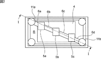
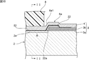
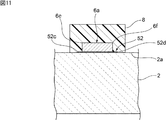
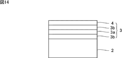
2…支持基板
2a,2b…第1,第2の主面
3…積層膜
3a…高音速膜
3b…低音速膜
3d…側面
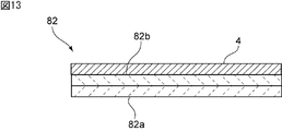
4…圧電薄膜
5a〜5c…IDT電極
6a〜6d…配線電極
6a1…傾斜面
6e…幅方向一端
6f…幅方向他端
7…中空空間
8…支持層
9…カバー部材
10a,10b…アンダーバンプメタル層
11a,11b…金属バンプ
12…第1の絶縁層
12a,12b…傾斜面
12c…内側端
22…第1の絶縁層
22a,22b…傾斜面
32…第1の絶縁層
32a…上面
32b,32c…傾斜面
52…第2の絶縁層
52c…幅方向一端
52d…幅方向他端
71…積層膜
82…積層膜
82a…高音響インピーダンス膜
82b…低音響インピーダンス膜
Claims (13)
- 支持基板と、
前記支持基板上に設けられており、圧電薄膜を含む複数の膜を有する積層膜と、
前記圧電薄膜の一方面に設けられたIDT電極と、
平面視において、前記IDT電極が設けられている領域の外側の領域において、前記積層膜が部分的に存在せず、前記積層膜が存在しない領域の少なくとも一部から、前記圧電薄膜上に至るように設けられた第1の絶縁層と、
前記IDT電極に電気的に接続されており、前記圧電薄膜上から前記第1の絶縁層上に至り、前記積層膜が存在しない領域に位置している前記第1の絶縁層部分上に至っている、配線電極と、
を備える、弾性波装置。 - 前記第1の絶縁層が前記圧電薄膜上から前記積層膜の側面を通り、前記積層膜が存在しない領域の少なくとも一部に至っている、請求項1に記載の弾性波装置。
- 前記第1の絶縁層上の前記支持基板とは反対側の面が、前記積層膜が存在しない領域から前記圧電薄膜上に位置している部分に近づくにつれて前記圧電薄膜側に近づくように傾斜している傾斜面を有する、請求項1または2に記載の弾性波装置。
- 前記第1の絶縁層の前記傾斜面が、前記支持基板上から前記圧電薄膜上の前記第1の絶縁層部分に至っている、請求項3に記載の弾性波装置。
- 前記第1の絶縁層が、前記傾斜面から前記積層膜が存在しないた領域に至っている、請求項3または4に記載の弾性波装置。
- 前記支持基板上において、前記配線電極が設けられている領域の一部を覆っており、かつ中空空間を構成するための開口部を有する支持層をさらに備え、前記支持層が、前記第1の絶縁層の前記傾斜面を越えて、前記圧電薄膜上の前記第1の絶縁層上に至っている、請求項4に記載の弾性波装置。
- 前記支持基板上に設けられており、中空空間を構成するための開口部を有する支持層をさらに備え、前記支持層が、前記支持基板上において、前記配線電極が設けられている領域から前記傾斜面の前記圧電薄膜側の端部まで至っている、請求項5に記載の弾性波装置。
- 前記配線電極と前記支持基板との間に設けられた第2の絶縁層をさらに備え、前記第2の絶縁層が、前記第1の絶縁層上に至っている、請求項1〜7のいずれか1項に記載の弾性波装置。
- 前記配線電極が延びる方向に対して直交する方向を幅方向とした場合、前記配線電極の前記幅方向における一端及び他端が、前記第2の絶縁層の前記幅方向における一端及び他端よりも前記幅方向において内側にそれぞれ位置している、請求項8に記載の弾性波装置。
- 前記傾斜面が、前記圧電薄膜側から前記積層膜が存在しない領域側に至るにつれて、前記支持基板側から遠ざかるように傾斜しており、前記第1の絶縁層が、前記圧電薄膜上よりも前記積層膜が存在しない領域において厚くされている、請求項4に記載の弾性波装置。
- 前記積層膜が、前記圧電薄膜と、前記圧電薄膜を伝搬する弾性波の音速よりも伝搬するバルク波の音速が低速である低音速膜とを有し、前記低音速膜上に、前記圧電薄膜が積層されている、請求項1〜10のいずれか1項に記載の弾性波装置。
- 前記積層膜が、前記圧電薄膜と、前記圧電薄膜を伝搬する弾性波の音速よりも伝搬するバルク波の音速が高速である高音速膜と、前記高音速膜上に積層されており、前記圧電薄膜を伝搬する弾性波の音速よりも伝搬するバルク波の音速が低速である低音速膜とを有し、前記低音速膜上に前記圧電薄膜が積層されている、請求項1〜10のいずれか1項に記載の弾性波装置。
- 前記積層膜が、前記圧電薄膜と、音響インピーダンスが相対的に高い高音響インピーダンス膜と、前記高音響インピーダンス膜に比べて音響インピーダンスが低い低音響インピーダンス膜とを有する、請求項1〜10のいずれか1項に記載の弾性波装置。
Applications Claiming Priority (3)
| Application Number | Priority Date | Filing Date | Title |
|---|---|---|---|
| JP2015127150 | 2015-06-25 | ||
| JP2015127150 | 2015-06-25 | ||
| PCT/JP2016/067409 WO2016208428A1 (ja) | 2015-06-25 | 2016-06-10 | 弾性波装置 |
Publications (2)
| Publication Number | Publication Date |
|---|---|
| JPWO2016208428A1 JPWO2016208428A1 (ja) | 2018-02-22 |
| JP6468357B2 true JP6468357B2 (ja) | 2019-02-13 |
Family
ID=57585575
Family Applications (1)
| Application Number | Title | Priority Date | Filing Date |
|---|---|---|---|
| JP2017525208A Active JP6468357B2 (ja) | 2015-06-25 | 2016-06-10 | 弾性波装置 |
Country Status (6)
| Country | Link |
|---|---|
| US (1) | US10659001B2 (ja) |
| JP (1) | JP6468357B2 (ja) |
| KR (1) | KR101929333B1 (ja) |
| CN (1) | CN107615659B (ja) |
| DE (1) | DE112016002839B4 (ja) |
| WO (1) | WO2016208428A1 (ja) |
Families Citing this family (12)
| Publication number | Priority date | Publication date | Assignee | Title |
|---|---|---|---|---|
| US10148245B2 (en) * | 2015-06-25 | 2018-12-04 | Murata Manufacturing Co., Ltd. | Elastic wave device |
| JP6432558B2 (ja) * | 2015-06-25 | 2018-12-05 | 株式会社村田製作所 | 弾性波装置 |
| JP6791390B2 (ja) | 2017-08-29 | 2020-11-25 | 株式会社村田製作所 | 弾性波装置、高周波フロントエンド回路及び通信装置 |
| CN111052607B (zh) | 2017-08-31 | 2023-10-17 | 株式会社村田制作所 | 弹性波装置以及具备该弹性波装置的弹性波模块 |
| CN111052606B (zh) * | 2017-08-31 | 2023-04-14 | 株式会社村田制作所 | 弹性波装置以及具备该弹性波装置的弹性波模块 |
| JP6950658B2 (ja) * | 2017-11-29 | 2021-10-13 | 株式会社村田製作所 | 弾性波装置 |
| US11677378B2 (en) * | 2017-11-29 | 2023-06-13 | Murata Manufacturing Co., Ltd. | Elastic wave device |
| JP7057690B2 (ja) * | 2018-03-19 | 2022-04-20 | 株式会社村田製作所 | 弾性波装置 |
| JP2019179961A (ja) | 2018-03-30 | 2019-10-17 | 株式会社村田製作所 | 弾性波装置 |
| JP2020205487A (ja) * | 2019-06-14 | 2020-12-24 | 株式会社村田製作所 | 弾性波装置 |
| WO2023037916A1 (ja) * | 2021-09-09 | 2023-03-16 | 株式会社村田製作所 | 弾性波装置 |
| CN116131801A (zh) * | 2023-02-17 | 2023-05-16 | 北京超材信息科技有限公司 | 声表面波器件及其制造方法 |
Family Cites Families (17)
| Publication number | Priority date | Publication date | Assignee | Title |
|---|---|---|---|---|
| US6426583B1 (en) * | 1999-06-14 | 2002-07-30 | Matsushita Electric Industrial Co., Ltd. | Surface acoustic wave element, method for producing the same and surface acoustic wave device using the same |
| JP2002261582A (ja) * | 2000-10-04 | 2002-09-13 | Matsushita Electric Ind Co Ltd | 弾性表面波デバイスおよびその製造方法ならびにそれを用いた回路モジュール |
| JP2004274574A (ja) * | 2003-03-11 | 2004-09-30 | Toyo Commun Equip Co Ltd | 弾性表面波装置とその製造方法 |
| JP2006121356A (ja) * | 2004-10-20 | 2006-05-11 | Seiko Epson Corp | 弾性表面波素子、電子デバイスおよび電子機器 |
| JP4904737B2 (ja) * | 2005-07-27 | 2012-03-28 | セイコーエプソン株式会社 | Ic一体型薄膜振動片の製造方法。 |
| JP2008060382A (ja) * | 2006-08-31 | 2008-03-13 | Matsushita Electric Ind Co Ltd | 電子部品及びその製造方法 |
| JP2009200093A (ja) | 2008-02-19 | 2009-09-03 | Murata Mfg Co Ltd | 中空型の電子部品 |
| CN104104356B (zh) * | 2008-11-28 | 2017-06-23 | 京瓷株式会社 | 弹性波装置及电路基板 |
| JP5713025B2 (ja) | 2010-12-24 | 2015-05-07 | 株式会社村田製作所 | 弾性波装置及びその製造方法 |
| JP5648695B2 (ja) * | 2010-12-24 | 2015-01-07 | 株式会社村田製作所 | 弾性波装置及びその製造方法 |
| JP6242597B2 (ja) | 2013-06-03 | 2017-12-06 | 太陽誘電株式会社 | 弾性波デバイス及びその製造方法 |
| CN105723615B (zh) * | 2013-11-29 | 2018-07-27 | 株式会社村田制作所 | 分波器 |
| JP2015109622A (ja) * | 2013-12-06 | 2015-06-11 | 株式会社村田製作所 | 縦結合共振子型弾性表面波フィルタ |
| JP6288110B2 (ja) | 2013-12-27 | 2018-03-07 | 株式会社村田製作所 | 弾性波装置 |
| JP6397352B2 (ja) * | 2015-02-19 | 2018-09-26 | 太陽誘電株式会社 | 弾性波デバイス |
| KR101989462B1 (ko) * | 2015-06-24 | 2019-06-14 | 가부시키가이샤 무라타 세이사쿠쇼 | 필터 장치 |
| US10148245B2 (en) * | 2015-06-25 | 2018-12-04 | Murata Manufacturing Co., Ltd. | Elastic wave device |
-
2016
- 2016-06-10 DE DE112016002839.3T patent/DE112016002839B4/de active Active
- 2016-06-10 CN CN201680031526.3A patent/CN107615659B/zh active Active
- 2016-06-10 KR KR1020177032063A patent/KR101929333B1/ko active IP Right Grant
- 2016-06-10 JP JP2017525208A patent/JP6468357B2/ja active Active
- 2016-06-10 WO PCT/JP2016/067409 patent/WO2016208428A1/ja active Application Filing
-
2017
- 2017-12-05 US US15/831,471 patent/US10659001B2/en active Active
Also Published As
| Publication number | Publication date |
|---|---|
| KR20170134666A (ko) | 2017-12-06 |
| JPWO2016208428A1 (ja) | 2018-02-22 |
| DE112016002839B4 (de) | 2022-01-13 |
| CN107615659B (zh) | 2020-11-17 |
| DE112016002839T5 (de) | 2018-03-08 |
| WO2016208428A1 (ja) | 2016-12-29 |
| US20180097502A1 (en) | 2018-04-05 |
| KR101929333B1 (ko) | 2018-12-14 |
| US10659001B2 (en) | 2020-05-19 |
| CN107615659A (zh) | 2018-01-19 |
Similar Documents
| Publication | Publication Date | Title |
|---|---|---|
| JP6468357B2 (ja) | 弾性波装置 | |
| JP6519655B2 (ja) | 弾性波装置 | |
| JP6516005B2 (ja) | 弾性波装置 | |
| US11218130B2 (en) | Acoustic wave device | |
| JP6432558B2 (ja) | 弾性波装置 | |
| US11539344B2 (en) | Elastic wave device and method for producing the same | |
| JP6566033B2 (ja) | マルチプレクサ、高周波フロントエンド回路及び通信装置 | |
| CN110324021B (zh) | 弹性波装置 | |
| WO2017013968A1 (ja) | 弾性波装置 | |
| WO2007007462A1 (ja) | 弾性境界波装置及びその製造方法 | |
| JP2019062350A (ja) | 複合素子 | |
| JP2015122566A (ja) | 弾性波装置 | |
| US10659002B2 (en) | Elastic wave device | |
| US20240154601A1 (en) | Acoustic wave device and method of manufacturing the same | |
| WO2022158363A1 (ja) | 弾性波装置 | |
| WO2023195409A1 (ja) | 弾性波装置および弾性波装置の製造方法 | |
| JP2016005162A (ja) | 電子部品装置 | |
| JP2020205487A (ja) | 弾性波装置 |
Legal Events
| Date | Code | Title | Description |
|---|---|---|---|
| A521 | Request for written amendment filed |
Free format text: JAPANESE INTERMEDIATE CODE: A523 Effective date: 20171020 |
|
| A621 | Written request for application examination |
Free format text: JAPANESE INTERMEDIATE CODE: A621 Effective date: 20171020 |
|
| TRDD | Decision of grant or rejection written | ||
| A01 | Written decision to grant a patent or to grant a registration (utility model) |
Free format text: JAPANESE INTERMEDIATE CODE: A01 Effective date: 20181218 |
|
| A61 | First payment of annual fees (during grant procedure) |
Free format text: JAPANESE INTERMEDIATE CODE: A61 Effective date: 20181231 |
|
| R150 | Certificate of patent or registration of utility model |
Ref document number: 6468357 Country of ref document: JP Free format text: JAPANESE INTERMEDIATE CODE: R150 |