JP6449766B2 - 光電子デバイス用透明電極 - Google Patents
光電子デバイス用透明電極 Download PDFInfo
- Publication number
- JP6449766B2 JP6449766B2 JP2015519470A JP2015519470A JP6449766B2 JP 6449766 B2 JP6449766 B2 JP 6449766B2 JP 2015519470 A JP2015519470 A JP 2015519470A JP 2015519470 A JP2015519470 A JP 2015519470A JP 6449766 B2 JP6449766 B2 JP 6449766B2
- Authority
- JP
- Japan
- Prior art keywords
- layer
- organic solar
- disposed
- intermediate layer
- metal
- Prior art date
- Legal status (The legal status is an assumption and is not a legal conclusion. Google has not performed a legal analysis and makes no representation as to the accuracy of the status listed.)
- Active
Links
- 230000005693 optoelectronics Effects 0.000 title description 13
- 239000010410 layer Substances 0.000 claims description 455
- 229910052751 metal Inorganic materials 0.000 claims description 37
- 239000002184 metal Substances 0.000 claims description 37
- 239000000758 substrate Substances 0.000 claims description 29
- 150000004706 metal oxides Chemical class 0.000 claims description 25
- 229910044991 metal oxide Inorganic materials 0.000 claims description 22
- 229910045601 alloy Inorganic materials 0.000 claims description 16
- 239000000956 alloy Substances 0.000 claims description 16
- 238000002207 thermal evaporation Methods 0.000 claims description 15
- 239000011368 organic material Substances 0.000 claims description 14
- 229910052709 silver Inorganic materials 0.000 claims description 14
- 229910052783 alkali metal Inorganic materials 0.000 claims description 8
- 150000001340 alkali metals Chemical class 0.000 claims description 8
- 150000001342 alkaline earth metals Chemical class 0.000 claims description 8
- 229910052784 alkaline earth metal Inorganic materials 0.000 claims description 7
- 229910052791 calcium Inorganic materials 0.000 claims description 7
- 229910052749 magnesium Inorganic materials 0.000 claims description 7
- 239000011241 protective layer Substances 0.000 claims description 6
- -1 oxides Chemical class 0.000 claims description 5
- 150000004767 nitrides Chemical class 0.000 claims description 3
- 229910015621 MoO Inorganic materials 0.000 claims description 2
- 150000004772 tellurides Chemical class 0.000 claims description 2
- 239000004332 silver Substances 0.000 claims 2
- 150000004771 selenides Chemical class 0.000 claims 1
- 150000004763 sulfides Chemical class 0.000 claims 1
- 239000000463 material Substances 0.000 description 53
- 238000000151 deposition Methods 0.000 description 30
- 230000008021 deposition Effects 0.000 description 17
- 238000004544 sputter deposition Methods 0.000 description 16
- 238000010521 absorption reaction Methods 0.000 description 11
- XMWRBQBLMFGWIX-UHFFFAOYSA-N C60 fullerene Chemical class C12=C3C(C4=C56)=C7C8=C5C5=C9C%10=C6C6=C4C1=C1C4=C6C6=C%10C%10=C9C9=C%11C5=C8C5=C8C7=C3C3=C7C2=C1C1=C2C4=C6C4=C%10C6=C9C9=C%11C5=C5C8=C3C3=C7C1=C1C2=C4C6=C2C9=C5C3=C12 XMWRBQBLMFGWIX-UHFFFAOYSA-N 0.000 description 10
- 229910010413 TiO 2 Inorganic materials 0.000 description 10
- 229910052737 gold Inorganic materials 0.000 description 8
- 239000010931 gold Substances 0.000 description 8
- 239000012044 organic layer Substances 0.000 description 8
- 229920000642 polymer Polymers 0.000 description 8
- 230000006798 recombination Effects 0.000 description 7
- 238000005215 recombination Methods 0.000 description 7
- 230000008901 benefit Effects 0.000 description 6
- 239000010409 thin film Substances 0.000 description 6
- 229910000287 alkaline earth metal oxide Inorganic materials 0.000 description 5
- 229910052782 aluminium Inorganic materials 0.000 description 5
- 239000002800 charge carrier Substances 0.000 description 5
- 238000001704 evaporation Methods 0.000 description 5
- 230000008020 evaporation Effects 0.000 description 5
- 229910003472 fullerene Inorganic materials 0.000 description 5
- 239000000203 mixture Substances 0.000 description 5
- IBHBKWKFFTZAHE-UHFFFAOYSA-N n-[4-[4-(n-naphthalen-1-ylanilino)phenyl]phenyl]-n-phenylnaphthalen-1-amine Chemical compound C1=CC=CC=C1N(C=1C2=CC=CC=C2C=CC=1)C1=CC=C(C=2C=CC(=CC=2)N(C=2C=CC=CC=2)C=2C3=CC=CC=C3C=CC=2)C=C1 IBHBKWKFFTZAHE-UHFFFAOYSA-N 0.000 description 5
- SBIBMFFZSBJNJF-UHFFFAOYSA-N selenium;zinc Chemical compound [Se]=[Zn] SBIBMFFZSBJNJF-UHFFFAOYSA-N 0.000 description 5
- 150000003384 small molecules Chemical class 0.000 description 5
- XLOMVQKBTHCTTD-UHFFFAOYSA-N Zinc monoxide Chemical compound [Zn]=O XLOMVQKBTHCTTD-UHFFFAOYSA-N 0.000 description 4
- 229910007709 ZnTe Inorganic materials 0.000 description 4
- 238000009792 diffusion process Methods 0.000 description 4
- 150000002343 gold Chemical class 0.000 description 4
- 238000007735 ion beam assisted deposition Methods 0.000 description 4
- 238000000034 method Methods 0.000 description 4
- 238000002156 mixing Methods 0.000 description 4
- JKQOBWVOAYFWKG-UHFFFAOYSA-N molybdenum trioxide Chemical compound O=[Mo](=O)=O JKQOBWVOAYFWKG-UHFFFAOYSA-N 0.000 description 4
- WLLGXSLBOPFWQV-UHFFFAOYSA-N MGK 264 Chemical compound C1=CC2CC1C1C2C(=O)N(CC(CC)CCCC)C1=O WLLGXSLBOPFWQV-UHFFFAOYSA-N 0.000 description 3
- XAGFODPZIPBFFR-UHFFFAOYSA-N aluminium Chemical compound [Al] XAGFODPZIPBFFR-UHFFFAOYSA-N 0.000 description 3
- 230000008859 change Effects 0.000 description 3
- ZUOUZKKEUPVFJK-UHFFFAOYSA-N diphenyl Chemical group C1=CC=CC=C1C1=CC=CC=C1 ZUOUZKKEUPVFJK-UHFFFAOYSA-N 0.000 description 3
- 239000002019 doping agent Substances 0.000 description 3
- 230000005684 electric field Effects 0.000 description 3
- 238000005566 electron beam evaporation Methods 0.000 description 3
- 229910052738 indium Inorganic materials 0.000 description 3
- 238000004519 manufacturing process Methods 0.000 description 3
- 239000000243 solution Substances 0.000 description 3
- 238000007740 vapor deposition Methods 0.000 description 3
- MQRCTQVBZYBPQE-UHFFFAOYSA-N 189363-47-1 Chemical compound C1=CC=CC=C1N(C=1C=C2C3(C4=CC(=CC=C4C2=CC=1)N(C=1C=CC=CC=1)C=1C=CC=CC=1)C1=CC(=CC=C1C1=CC=C(C=C13)N(C=1C=CC=CC=1)C=1C=CC=CC=1)N(C=1C=CC=CC=1)C=1C=CC=CC=1)C1=CC=CC=C1 MQRCTQVBZYBPQE-UHFFFAOYSA-N 0.000 description 2
- PONZBUKBFVIXOD-UHFFFAOYSA-N 9,10-dicarbamoylperylene-3,4-dicarboxylic acid Chemical class C=12C3=CC=C(C(O)=O)C2=C(C(O)=O)C=CC=1C1=CC=C(C(O)=N)C2=C1C3=CC=C2C(=N)O PONZBUKBFVIXOD-UHFFFAOYSA-N 0.000 description 2
- 238000000862 absorption spectrum Methods 0.000 description 2
- 230000015572 biosynthetic process Effects 0.000 description 2
- 230000000903 blocking effect Effects 0.000 description 2
- 229910052804 chromium Inorganic materials 0.000 description 2
- 239000004020 conductor Substances 0.000 description 2
- 229910052802 copper Inorganic materials 0.000 description 2
- 239000013078 crystal Substances 0.000 description 2
- 238000010586 diagram Methods 0.000 description 2
- BKMIWBZIQAAZBD-UHFFFAOYSA-N diindenoperylene Chemical compound C12=C3C4=CC=C2C2=CC=CC=C2C1=CC=C3C1=CC=C2C3=CC=CC=C3C3=CC=C4C1=C32 BKMIWBZIQAAZBD-UHFFFAOYSA-N 0.000 description 2
- QXYJCZRRLLQGCR-UHFFFAOYSA-N dioxomolybdenum Chemical compound O=[Mo]=O QXYJCZRRLLQGCR-UHFFFAOYSA-N 0.000 description 2
- 238000000605 extraction Methods 0.000 description 2
- 239000011521 glass Substances 0.000 description 2
- 230000009477 glass transition Effects 0.000 description 2
- PCHJSUWPFVWCPO-UHFFFAOYSA-N gold Chemical compound [Au] PCHJSUWPFVWCPO-UHFFFAOYSA-N 0.000 description 2
- 230000005525 hole transport Effects 0.000 description 2
- 239000011229 interlayer Substances 0.000 description 2
- 238000007733 ion plating Methods 0.000 description 2
- 229910052746 lanthanum Inorganic materials 0.000 description 2
- 230000031700 light absorption Effects 0.000 description 2
- 238000001451 molecular beam epitaxy Methods 0.000 description 2
- YTVNOVQHSGMMOV-UHFFFAOYSA-N naphthalenetetracarboxylic dianhydride Chemical compound C1=CC(C(=O)OC2=O)=C3C2=CC=C2C(=O)OC(=O)C1=C32 YTVNOVQHSGMMOV-UHFFFAOYSA-N 0.000 description 2
- 230000003287 optical effect Effects 0.000 description 2
- 125000002080 perylenyl group Chemical class C1(=CC=C2C=CC=C3C4=CC=CC5=CC=CC(C1=C23)=C45)* 0.000 description 2
- 229910052697 platinum Inorganic materials 0.000 description 2
- 230000008569 process Effects 0.000 description 2
- 239000000047 product Substances 0.000 description 2
- 150000003346 selenoethers Chemical class 0.000 description 2
- 239000004065 semiconductor Substances 0.000 description 2
- 238000000926 separation method Methods 0.000 description 2
- 229910052712 strontium Inorganic materials 0.000 description 2
- FHCPAXDKURNIOZ-UHFFFAOYSA-N tetrathiafulvalene Chemical class S1C=CSC1=C1SC=CS1 FHCPAXDKURNIOZ-UHFFFAOYSA-N 0.000 description 2
- 229910052718 tin Inorganic materials 0.000 description 2
- 229910052719 titanium Inorganic materials 0.000 description 2
- 238000002834 transmittance Methods 0.000 description 2
- 239000012780 transparent material Substances 0.000 description 2
- 229910052725 zinc Inorganic materials 0.000 description 2
- 239000011701 zinc Substances 0.000 description 2
- 239000011787 zinc oxide Substances 0.000 description 2
- 229910052726 zirconium Inorganic materials 0.000 description 2
- 125000001637 1-naphthyl group Chemical group [H]C1=C([H])C([H])=C2C(*)=C([H])C([H])=C([H])C2=C1[H] 0.000 description 1
- IXHWGNYCZPISET-UHFFFAOYSA-N 2-[4-(dicyanomethylidene)-2,3,5,6-tetrafluorocyclohexa-2,5-dien-1-ylidene]propanedinitrile Chemical compound FC1=C(F)C(=C(C#N)C#N)C(F)=C(F)C1=C(C#N)C#N IXHWGNYCZPISET-UHFFFAOYSA-N 0.000 description 1
- WPUSEOSICYGUEW-UHFFFAOYSA-N 4-[4-(4-methoxy-n-(4-methoxyphenyl)anilino)phenyl]-n,n-bis(4-methoxyphenyl)aniline Chemical compound C1=CC(OC)=CC=C1N(C=1C=CC(=CC=1)C=1C=CC(=CC=1)N(C=1C=CC(OC)=CC=1)C=1C=CC(OC)=CC=1)C1=CC=C(OC)C=C1 WPUSEOSICYGUEW-UHFFFAOYSA-N 0.000 description 1
- 125000004172 4-methoxyphenyl group Chemical group [H]C1=C([H])C(OC([H])([H])[H])=C([H])C([H])=C1* 0.000 description 1
- DIVZFUBWFAOMCW-UHFFFAOYSA-N 4-n-(3-methylphenyl)-1-n,1-n-bis[4-(n-(3-methylphenyl)anilino)phenyl]-4-n-phenylbenzene-1,4-diamine Chemical compound CC1=CC=CC(N(C=2C=CC=CC=2)C=2C=CC(=CC=2)N(C=2C=CC(=CC=2)N(C=2C=CC=CC=2)C=2C=C(C)C=CC=2)C=2C=CC(=CC=2)N(C=2C=CC=CC=2)C=2C=C(C)C=CC=2)=C1 DIVZFUBWFAOMCW-UHFFFAOYSA-N 0.000 description 1
- CRHRWHRNQKPUPO-UHFFFAOYSA-N 4-n-naphthalen-1-yl-1-n,1-n-bis[4-(n-naphthalen-1-ylanilino)phenyl]-4-n-phenylbenzene-1,4-diamine Chemical compound C1=CC=CC=C1N(C=1C2=CC=CC=C2C=CC=1)C1=CC=C(N(C=2C=CC(=CC=2)N(C=2C=CC=CC=2)C=2C3=CC=CC=C3C=CC=2)C=2C=CC(=CC=2)N(C=2C=CC=CC=2)C=2C3=CC=CC=C3C=CC=2)C=C1 CRHRWHRNQKPUPO-UHFFFAOYSA-N 0.000 description 1
- JBRZTFJDHDCESZ-UHFFFAOYSA-N AsGa Chemical compound [As]#[Ga] JBRZTFJDHDCESZ-UHFFFAOYSA-N 0.000 description 1
- OKTJSMMVPCPJKN-UHFFFAOYSA-N Carbon Chemical compound [C] OKTJSMMVPCPJKN-UHFFFAOYSA-N 0.000 description 1
- 229910001218 Gallium arsenide Inorganic materials 0.000 description 1
- 229910015711 MoOx Inorganic materials 0.000 description 1
- XUIMIQQOPSSXEZ-UHFFFAOYSA-N Silicon Chemical compound [Si] XUIMIQQOPSSXEZ-UHFFFAOYSA-N 0.000 description 1
- UCKMPCXJQFINFW-UHFFFAOYSA-N Sulphide Chemical compound [S-2] UCKMPCXJQFINFW-UHFFFAOYSA-N 0.000 description 1
- 239000002253 acid Substances 0.000 description 1
- 230000009471 action Effects 0.000 description 1
- 239000012790 adhesive layer Substances 0.000 description 1
- 229910001508 alkali metal halide Inorganic materials 0.000 description 1
- 150000008045 alkali metal halides Chemical class 0.000 description 1
- 229910001615 alkaline earth metal halide Inorganic materials 0.000 description 1
- 229910021417 amorphous silicon Inorganic materials 0.000 description 1
- 239000006117 anti-reflective coating Substances 0.000 description 1
- 239000012298 atmosphere Substances 0.000 description 1
- QVGXLLKOCUKJST-UHFFFAOYSA-N atomic oxygen Chemical compound [O] QVGXLLKOCUKJST-UHFFFAOYSA-N 0.000 description 1
- 230000009286 beneficial effect Effects 0.000 description 1
- 230000005540 biological transmission Effects 0.000 description 1
- 235000010290 biphenyl Nutrition 0.000 description 1
- 239000000872 buffer Substances 0.000 description 1
- 229910052792 caesium Inorganic materials 0.000 description 1
- 239000003990 capacitor Substances 0.000 description 1
- 238000000541 cathodic arc deposition Methods 0.000 description 1
- 239000007795 chemical reaction product Substances 0.000 description 1
- 230000000295 complement effect Effects 0.000 description 1
- 150000001875 compounds Chemical class 0.000 description 1
- RPHPLYFQXFWMRH-UHFFFAOYSA-N ctk2f8269 Chemical group C=12C3=CC=CC2=CC=CC=1C1=C2C=CC=CC2=CC2=C1C3=CC1=CC=CC=C21 RPHPLYFQXFWMRH-UHFFFAOYSA-N 0.000 description 1
- 238000000354 decomposition reaction Methods 0.000 description 1
- 230000032798 delamination Effects 0.000 description 1
- 230000001419 dependent effect Effects 0.000 description 1
- 238000005137 deposition process Methods 0.000 description 1
- RAABOESOVLLHRU-UHFFFAOYSA-N diazene Chemical compound N=N RAABOESOVLLHRU-UHFFFAOYSA-N 0.000 description 1
- 229910000071 diazene Inorganic materials 0.000 description 1
- 239000000539 dimer Substances 0.000 description 1
- HKNRNTYTYUWGLN-UHFFFAOYSA-N dithieno[3,2-a:2',3'-d]thiophene Chemical compound C1=CSC2=C1SC1=C2C=CS1 HKNRNTYTYUWGLN-UHFFFAOYSA-N 0.000 description 1
- 230000000694 effects Effects 0.000 description 1
- 238000004146 energy storage Methods 0.000 description 1
- 238000005516 engineering process Methods 0.000 description 1
- 230000005281 excited state Effects 0.000 description 1
- 230000001747 exhibiting effect Effects 0.000 description 1
- 239000004744 fabric Substances 0.000 description 1
- 239000003574 free electron Substances 0.000 description 1
- 229910052733 gallium Inorganic materials 0.000 description 1
- 239000007789 gas Substances 0.000 description 1
- 229910021389 graphene Inorganic materials 0.000 description 1
- 229910052735 hafnium Inorganic materials 0.000 description 1
- 238000010438 heat treatment Methods 0.000 description 1
- 238000004770 highest occupied molecular orbital Methods 0.000 description 1
- 239000012535 impurity Substances 0.000 description 1
- 238000002347 injection Methods 0.000 description 1
- 239000007924 injection Substances 0.000 description 1
- 238000000608 laser ablation Methods 0.000 description 1
- 229910052744 lithium Inorganic materials 0.000 description 1
- 238000004768 lowest unoccupied molecular orbital Methods 0.000 description 1
- 230000007246 mechanism Effects 0.000 description 1
- 230000008018 melting Effects 0.000 description 1
- 238000002844 melting Methods 0.000 description 1
- 239000002923 metal particle Substances 0.000 description 1
- 229910000476 molybdenum oxide Inorganic materials 0.000 description 1
- 239000002070 nanowire Substances 0.000 description 1
- MZYHMUONCNKCHE-UHFFFAOYSA-N naphthalene-1,2,3,4-tetracarboxylic acid Chemical compound C1=CC=CC2=C(C(O)=O)C(C(=O)O)=C(C(O)=O)C(C(O)=O)=C21 MZYHMUONCNKCHE-UHFFFAOYSA-N 0.000 description 1
- 230000007935 neutral effect Effects 0.000 description 1
- NIHNNTQXNPWCJQ-UHFFFAOYSA-N o-biphenylenemethane Natural products C1=CC=C2CC3=CC=CC=C3C2=C1 NIHNNTQXNPWCJQ-UHFFFAOYSA-N 0.000 description 1
- PQQKPALAQIIWST-UHFFFAOYSA-N oxomolybdenum Chemical compound [Mo]=O PQQKPALAQIIWST-UHFFFAOYSA-N 0.000 description 1
- 229910052760 oxygen Inorganic materials 0.000 description 1
- 239000001301 oxygen Substances 0.000 description 1
- 230000003071 parasitic effect Effects 0.000 description 1
- 230000035515 penetration Effects 0.000 description 1
- 150000002964 pentacenes Chemical class 0.000 description 1
- 230000035699 permeability Effects 0.000 description 1
- PJQYNUFEEZFYIS-UHFFFAOYSA-N perylene maroon Chemical compound C=12C3=CC=C(C(N(C)C4=O)=O)C2=C4C=CC=1C1=CC=C2C(=O)N(C)C(=O)C4=CC=C3C1=C42 PJQYNUFEEZFYIS-UHFFFAOYSA-N 0.000 description 1
- 125000001997 phenyl group Chemical group [H]C1=C([H])C([H])=C(*)C([H])=C1[H] 0.000 description 1
- IEQIEDJGQAUEQZ-UHFFFAOYSA-N phthalocyanine Chemical compound N1C(N=C2C3=CC=CC=C3C(N=C3C4=CC=CC=C4C(=N4)N3)=N2)=C(C=CC=C2)C2=C1N=C1C2=CC=CC=C2C4=N1 IEQIEDJGQAUEQZ-UHFFFAOYSA-N 0.000 description 1
- 150000004033 porphyrin derivatives Chemical class 0.000 description 1
- 238000004549 pulsed laser deposition Methods 0.000 description 1
- 238000005546 reactive sputtering Methods 0.000 description 1
- 230000009467 reduction Effects 0.000 description 1
- 238000002310 reflectometry Methods 0.000 description 1
- 229910052706 scandium Inorganic materials 0.000 description 1
- 229910052711 selenium Inorganic materials 0.000 description 1
- 229910052710 silicon Inorganic materials 0.000 description 1
- 239000010703 silicon Substances 0.000 description 1
- 239000002356 single layer Substances 0.000 description 1
- 239000002904 solvent Substances 0.000 description 1
- 230000003595 spectral effect Effects 0.000 description 1
- 150000003413 spiro compounds Chemical class 0.000 description 1
- 239000000126 substance Substances 0.000 description 1
- 229910052717 sulfur Inorganic materials 0.000 description 1
- 238000003786 synthesis reaction Methods 0.000 description 1
- XSOKHXFFCGXDJZ-UHFFFAOYSA-N telluride(2-) Chemical compound [Te-2] XSOKHXFFCGXDJZ-UHFFFAOYSA-N 0.000 description 1
- 150000003568 thioethers Chemical class 0.000 description 1
- 229910052723 transition metal Inorganic materials 0.000 description 1
- 150000003624 transition metals Chemical class 0.000 description 1
- ODHXBMXNKOYIBV-UHFFFAOYSA-N triphenylamine Chemical class C1=CC=CC=C1N(C=1C=CC=CC=1)C1=CC=CC=C1 ODHXBMXNKOYIBV-UHFFFAOYSA-N 0.000 description 1
- 230000005641 tunneling Effects 0.000 description 1
- XLYOFNOQVPJJNP-UHFFFAOYSA-N water Substances O XLYOFNOQVPJJNP-UHFFFAOYSA-N 0.000 description 1
Images


Classifications
-
- H—ELECTRICITY
- H10—SEMICONDUCTOR DEVICES; ELECTRIC SOLID-STATE DEVICES NOT OTHERWISE PROVIDED FOR
- H10K—ORGANIC ELECTRIC SOLID-STATE DEVICES
- H10K30/00—Organic devices sensitive to infrared radiation, light, electromagnetic radiation of shorter wavelength or corpuscular radiation
- H10K30/80—Constructional details
- H10K30/81—Electrodes
- H10K30/82—Transparent electrodes, e.g. indium tin oxide [ITO] electrodes
-
- H—ELECTRICITY
- H01—ELECTRIC ELEMENTS
- H01L—SEMICONDUCTOR DEVICES NOT COVERED BY CLASS H10
- H01L31/00—Semiconductor devices sensitive to infrared radiation, light, electromagnetic radiation of shorter wavelength or corpuscular radiation and specially adapted either for the conversion of the energy of such radiation into electrical energy or for the control of electrical energy by such radiation; Processes or apparatus specially adapted for the manufacture or treatment thereof or of parts thereof; Details thereof
- H01L31/0248—Semiconductor devices sensitive to infrared radiation, light, electromagnetic radiation of shorter wavelength or corpuscular radiation and specially adapted either for the conversion of the energy of such radiation into electrical energy or for the control of electrical energy by such radiation; Processes or apparatus specially adapted for the manufacture or treatment thereof or of parts thereof; Details thereof characterised by their semiconductor bodies
- H01L31/0256—Semiconductor devices sensitive to infrared radiation, light, electromagnetic radiation of shorter wavelength or corpuscular radiation and specially adapted either for the conversion of the energy of such radiation into electrical energy or for the control of electrical energy by such radiation; Processes or apparatus specially adapted for the manufacture or treatment thereof or of parts thereof; Details thereof characterised by their semiconductor bodies characterised by the material
- H01L2031/0344—Organic materials
-
- H—ELECTRICITY
- H10—SEMICONDUCTOR DEVICES; ELECTRIC SOLID-STATE DEVICES NOT OTHERWISE PROVIDED FOR
- H10K—ORGANIC ELECTRIC SOLID-STATE DEVICES
- H10K30/00—Organic devices sensitive to infrared radiation, light, electromagnetic radiation of shorter wavelength or corpuscular radiation
- H10K30/40—Organic devices sensitive to infrared radiation, light, electromagnetic radiation of shorter wavelength or corpuscular radiation comprising a p-i-n structure, e.g. having a perovskite absorber between p-type and n-type charge transport layers
-
- H—ELECTRICITY
- H10—SEMICONDUCTOR DEVICES; ELECTRIC SOLID-STATE DEVICES NOT OTHERWISE PROVIDED FOR
- H10K—ORGANIC ELECTRIC SOLID-STATE DEVICES
- H10K50/00—Organic light-emitting devices
- H10K50/80—Constructional details
- H10K50/805—Electrodes
- H10K50/82—Cathodes
- H10K50/826—Multilayers, e.g. opaque multilayers
-
- H—ELECTRICITY
- H10—SEMICONDUCTOR DEVICES; ELECTRIC SOLID-STATE DEVICES NOT OTHERWISE PROVIDED FOR
- H10K—ORGANIC ELECTRIC SOLID-STATE DEVICES
- H10K71/00—Manufacture or treatment specially adapted for the organic devices covered by this subclass
- H10K71/60—Forming conductive regions or layers, e.g. electrodes
-
- Y—GENERAL TAGGING OF NEW TECHNOLOGICAL DEVELOPMENTS; GENERAL TAGGING OF CROSS-SECTIONAL TECHNOLOGIES SPANNING OVER SEVERAL SECTIONS OF THE IPC; TECHNICAL SUBJECTS COVERED BY FORMER USPC CROSS-REFERENCE ART COLLECTIONS [XRACs] AND DIGESTS
- Y02—TECHNOLOGIES OR APPLICATIONS FOR MITIGATION OR ADAPTATION AGAINST CLIMATE CHANGE
- Y02B—CLIMATE CHANGE MITIGATION TECHNOLOGIES RELATED TO BUILDINGS, e.g. HOUSING, HOUSE APPLIANCES OR RELATED END-USER APPLICATIONS
- Y02B10/00—Integration of renewable energy sources in buildings
- Y02B10/10—Photovoltaic [PV]
-
- Y—GENERAL TAGGING OF NEW TECHNOLOGICAL DEVELOPMENTS; GENERAL TAGGING OF CROSS-SECTIONAL TECHNOLOGIES SPANNING OVER SEVERAL SECTIONS OF THE IPC; TECHNICAL SUBJECTS COVERED BY FORMER USPC CROSS-REFERENCE ART COLLECTIONS [XRACs] AND DIGESTS
- Y02—TECHNOLOGIES OR APPLICATIONS FOR MITIGATION OR ADAPTATION AGAINST CLIMATE CHANGE
- Y02E—REDUCTION OF GREENHOUSE GAS [GHG] EMISSIONS, RELATED TO ENERGY GENERATION, TRANSMISSION OR DISTRIBUTION
- Y02E10/00—Energy generation through renewable energy sources
- Y02E10/50—Photovoltaic [PV] energy
- Y02E10/549—Organic PV cells
-
- Y—GENERAL TAGGING OF NEW TECHNOLOGICAL DEVELOPMENTS; GENERAL TAGGING OF CROSS-SECTIONAL TECHNOLOGIES SPANNING OVER SEVERAL SECTIONS OF THE IPC; TECHNICAL SUBJECTS COVERED BY FORMER USPC CROSS-REFERENCE ART COLLECTIONS [XRACs] AND DIGESTS
- Y02—TECHNOLOGIES OR APPLICATIONS FOR MITIGATION OR ADAPTATION AGAINST CLIMATE CHANGE
- Y02P—CLIMATE CHANGE MITIGATION TECHNOLOGIES IN THE PRODUCTION OR PROCESSING OF GOODS
- Y02P70/00—Climate change mitigation technologies in the production process for final industrial or consumer products
- Y02P70/50—Manufacturing or production processes characterised by the final manufactured product
Description
非有機太陽電池セルとは対照的に、有機太陽電池セルの場合は、光によって直接電荷キャリアが生成されるのではなく、まずエキシトン、すなわち電気的に中性な励起状態(束縛された電子−正孔対)が形成される。漸く第2のステップにおいて、これらのエキシトンは、自由電荷キャリアに分離され、これらはこうして電流フローに寄与する。
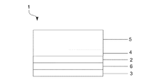
0. 担体,基板
1. 基板側接続部(Grundkontakt)、通常透明
2. p層(複数でもよい)
3. i層(複数でもよい)
4. n層(複数でもよい)
5. 上側接続部(Deckkontakt)
このタンデムセルは、たとえばpinpin構造(またはたとえばnipnipであってもよい)を備える。上記の2つのpin部分セルの間の界面には、それぞれに1つのnドーピングされた層と1つのpドーピングされた層が存在し、これらはpn系(あるいはnp系)を形成している。このようなpn系においては、電子と正孔との極めて効率的な再結合が起こる。2つのpinユニットセルの積層は、これによって、さらなる層を必要とせずに、そのまま1つの完全なpinタンデムセルを形成する。ここで、平本の場合のように、効率的な再結合を確実にするための、薄い金属層がもはや必要でないということは、とりわけ有利である。これによってこのような薄い金属層の吸収損失を完全に避けることができる。
さらに加えてこの論文には、このAg層の下に、このAg層の平坦化のために薄いAlの中間層を用いることを開示している。またここには、トップコンタクトの透明性を高めるために、この薄いAg層上に有機層を用いることが示されている。
1)熱的蒸着に対して、これらの代替の堆積方法を用いて、より平坦な層を生成することができ、極めて薄い層において、基板の平面に既に高い導電性を有する閉じた層を実現することができる。僅かな層厚のおかげで、この層の高い透過性が達成され、同時に(この平面における)充分な導電性が達成される。2)熱的蒸着に対して、上記の堆積方法を用いて、基板上の層厚の高度な均一性をもたらすことができる。これは薄いトップコンタクト層の場合は特に重要である。これは上記の第2の層の層厚における変化がデバイスの性能に直接影響を与え、このデバイスの光学的効果の目に見える変化をもたらすからであり、これは一般的に好ましいものでない。3)これらの代替の堆積方法を用いることによって、熱的蒸着に対して、さらに多数の様々な材料を、(たとえば反応性スパッタリングの)プロセスパラメータを大きく変化させて用いることができる。
この層がデバイスの層間の応力を低減するのに寄与すると考えられる。このような層間の応力は、たとえば異なる熱膨張係数(膨張係数等)のために生じ得るが、これは最も深刻な場合には部分的または全体的な層の剥離をもたらし得る。
小分子とは、本発明での意味は、蒸発されて基板上に堆積することができるものである。
ここでワイドギャップ層とは450nmより短い波長領域で吸収ピークを有する層のことである。
ここでこれらの実施形態例は、本発明を説明するものであるが、本発明を限定するものではない。
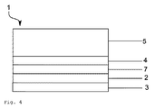
2 第1の層
3 第1の中間層
4 第2の層
5 スクラッチ保護層
6 第2の中間層
7 第3の中間層
Claims (14)
- 第1および第2の電極を備えた基板上の有機太陽電池セルであって、
前記第1の電極は、前記基板上に配設されており、前記第2の電極は対向電極を形成し、
前記第1の電極と前記第2の電極との間に、少なくとも1つの光活性な層系が配設されており、当該層系は、有機材料を含む少なくとも1つのドナー−アクセプター系を備え、
前記対向電極(1)は、少なくとも1つの第1の層(2)と、当該第1の層(2)と前記有機太陽電池セルの前記光活性な層系との間に配設されている1つの第1の中間層(3)と、当該第1の層(2)上に配設されている1つの第2の層(4)とを備え、前記第1の中間層(3)と前記対向電極の前記第1の層(2)との間に、金属または金属酸化物からなる第2の中間層(6)が挿入されており、当該第2の中間層(6)は、0.05〜30nmの層厚を有し、当該第1の層(2)は、銀、または銀を含む合金を含み、当該第1の中間層(3)はCa,Mg,またはMoOxを含み、当該第2の層(4)は、10〜100nmの層厚および2より大きい屈折率を有し、
前記対向電極(1)と前記光活性な層系の間には、1つの、ドーピングされた輸送層,部分的にドーピングされた輸送層,またはドーピングされていない輸送層が配設されている、
ことを特徴とする有機太陽電池セル。 - 前記第1の層(2)は、AgおよびCaから成る合金、またはAgおよびMgから成る合金を含むことを特徴とする、請求項1に記載の有機太陽電池セル。
- 前記第1の層(2)は、AgおよびCaから成る合金、またはAgおよびMgから成る合金を含み、AgまたはCaまたはMgの割合は、少なくとも30%であることを特徴とする、請求項1または2に記載の有機太陽電池セル。
- 前記対向電極の前記第1の中間層(3)は、0.1〜100nmの層厚の熱蒸着層を有することを特徴とする、請求項1乃至3のいずれか1項に記載の有機太陽電池セル。
- 前記対向電極(1)の前記第1の層(2)は、3〜20nmの層厚を有することを特徴とする、請求項1乃至4のいずれか1項に記載の有機太陽電池セル。
- 前記対向電極(1)の前記第1の層(2)は、5〜10nmの層厚を有することを特徴とする、請求項1乃至5のいずれか1項に記載の有機太陽電池セル。
- 前記第2の層(4)は、アルカリ金属またはアルカリ土類金属,金属酸化物または有機材料を含むことを特徴とする、請求項1乃至6のいずれか1項に記載の有機太陽電池セル。
- 前記第2の層(4)は、窒化物,セレン化物,硫化物,酸化物,テルル化物,またはポリマーを含むことを特徴とする、請求項1乃至7のいずれか1項に記載の有機太陽電池セル。
- 前記第2の層(4)は、2.2より大きい屈折率を有することを特徴とする、請求項1乃至8のいずれか1項に記載の有機太陽電池セル。
- 前記第2の層(4)上に、酸化物を含みかつ層厚が100nmより大きい保護層(5)が配設されていることを特徴とする、請求項1乃至9のいずれか1項に記載の有機太陽電池セル。
- 前記対向電極(1)の前記第1の層(2)と前記第2の層(4)との間には、金属または金属酸化物から成るもう1つの中間層(7)が挿入されていることを特徴とする、請求項1乃至10のいずれか1項に記載の有機太陽電池セル。
- 前記基板は不透明または透明に実装されていることを特徴とする、請求項1乃至11のいずれか1項に記載の有機太陽電池セル。
- 前記基板は可撓に実装されていることを特徴とする、請求項1乃至12のいずれか1項に記載の有機太陽電池セル。
- 前記有機太陽電池セルは、pinシングルセル,pinタンデムセル,pin多層セル,nipシングルセル,nipタンデムセル,またはnip多層セルであることを特徴とする、請求項1乃至13のいずれか1項に記載の有機太陽電池セル。
Applications Claiming Priority (5)
| Application Number | Priority Date | Filing Date | Title |
|---|---|---|---|
| DE102012105810.5 | 2012-07-02 | ||
| DE102012105810.5A DE102012105810B4 (de) | 2012-07-02 | 2012-07-02 | Transparente Elektrode für optoelektronische Bauelemente |
| DE102012105809.1A DE102012105809B4 (de) | 2012-07-02 | 2012-07-02 | Organisches optoelektronisches Bauelement mit transparenter Gegenelektrode und transparenter Elektrodenvorrichtung |
| DE102012105809.1 | 2012-07-02 | ||
| PCT/IB2013/055425 WO2014006565A2 (de) | 2012-07-02 | 2013-07-02 | Transparente elektrode für optoelektronische bauelemente |
Publications (3)
| Publication Number | Publication Date |
|---|---|
| JP2015527732A JP2015527732A (ja) | 2015-09-17 |
| JP2015527732A5 JP2015527732A5 (ja) | 2016-08-04 |
| JP6449766B2 true JP6449766B2 (ja) | 2019-01-09 |
Family
ID=49223810
Family Applications (1)
| Application Number | Title | Priority Date | Filing Date |
|---|---|---|---|
| JP2015519470A Active JP6449766B2 (ja) | 2012-07-02 | 2013-07-02 | 光電子デバイス用透明電極 |
Country Status (8)
| Country | Link |
|---|---|
| US (1) | US11355719B2 (ja) |
| EP (1) | EP2867932B1 (ja) |
| JP (1) | JP6449766B2 (ja) |
| KR (1) | KR102128943B1 (ja) |
| CN (1) | CN104584252B (ja) |
| BR (1) | BR112014033108B1 (ja) |
| ES (1) | ES2762410T3 (ja) |
| WO (1) | WO2014006565A2 (ja) |
Families Citing this family (7)
| Publication number | Priority date | Publication date | Assignee | Title |
|---|---|---|---|---|
| KR102612902B1 (ko) | 2016-04-22 | 2023-12-18 | 삼성디스플레이 주식회사 | 투명 전도막 및 이를 포함하는 전자 소자 |
| KR102097517B1 (ko) | 2016-06-23 | 2020-04-06 | 코오롱인더스트리 주식회사 | 반투명 유기 태양전지 및 이의 제조 방법 |
| KR20170141407A (ko) * | 2016-06-15 | 2017-12-26 | 코오롱인더스트리 주식회사 | 유기 태양전지 및 이의 제조 방법 |
| KR102113536B1 (ko) * | 2017-03-20 | 2020-05-21 | 코오롱인더스트리 주식회사 | 반투명 유기 태양전지 모듈 |
| CN107068864B (zh) | 2017-04-14 | 2019-05-28 | 武汉华星光电技术有限公司 | 有机薄膜晶体管的制作方法 |
| WO2019102478A1 (en) * | 2017-11-26 | 2019-05-31 | Ramot At Tel-Aviv University Ltd. | Device and method for neurostimulation |
| DE102019216327A1 (de) * | 2019-10-23 | 2021-04-29 | Fraunhofer-Gesellschaft zur Förderung der angewandten Forschung e.V. | Sensor mit einer festkörper-schichtstruktur und verfahren zur herstellung eines sensors |
Family Cites Families (45)
| Publication number | Priority date | Publication date | Assignee | Title |
|---|---|---|---|---|
| CA1085947A (en) | 1977-08-02 | 1980-09-16 | Ching W. Tang | Multilayer organic photovoltaic elements |
| US5093698A (en) | 1991-02-12 | 1992-03-03 | Kabushiki Kaisha Toshiba | Organic electroluminescent device |
| JP2538479Y2 (ja) | 1991-11-06 | 1997-06-18 | 三洋電機株式会社 | 光起電力装置 |
| JP3300069B2 (ja) * | 1992-11-19 | 2002-07-08 | パイオニア株式会社 | 有機エレクトロルミネッセンス素子 |
| AU736457B2 (en) * | 1997-08-27 | 2001-07-26 | Sphelar Power Corporation | Spherical semiconductor device and the manufacture method for the same and spherical semiconductor device material |
| US6198092B1 (en) * | 1998-08-19 | 2001-03-06 | The Trustees Of Princeton University | Stacked organic photosensitive optoelectronic devices with an electrically parallel configuration |
| DE19905694A1 (de) | 1998-11-27 | 2000-08-17 | Forschungszentrum Juelich Gmbh | Bauelement |
| JP2002532849A (ja) * | 1998-12-17 | 2002-10-02 | ケンブリッジ ディスプレイ テクノロジー リミテッド | 有機発光デバイスの製造方法 |
| JP2004119129A (ja) | 2002-09-25 | 2004-04-15 | Tokai Rubber Ind Ltd | 色素増感型太陽電池の製法およびそれによって得られた色素増感型太陽電池 |
| AU2004221377B2 (en) | 2003-03-19 | 2009-07-16 | Heliatek Gmbh | Photoactive component comprising organic layers |
| US20040211458A1 (en) | 2003-04-28 | 2004-10-28 | General Electric Company | Tandem photovoltaic cell stacks |
| DE10338406A1 (de) | 2003-08-18 | 2005-03-24 | Novaled Gmbh | Dotierte organische Halbleitermaterialien sowie Verfahren zu deren Herstellung |
| US7411223B2 (en) | 2003-09-15 | 2008-08-12 | General Electric Company | Compound electrodes for electronic devices |
| DE10347856B8 (de) | 2003-10-10 | 2006-10-19 | Colorado State University Research Foundation, Fort Collins | Halbleiterdotierung |
| US7061011B2 (en) | 2003-11-26 | 2006-06-13 | The Trustees Of Princeton University | Bipolar organic devices |
| DE10357044A1 (de) | 2003-12-04 | 2005-07-14 | Novaled Gmbh | Verfahren zur Dotierung von organischen Halbleitern mit Chinondiiminderivaten |
| DE102004010954A1 (de) | 2004-03-03 | 2005-10-06 | Novaled Gmbh | Verwendung eines Metallkomplexes als n-Dotand für ein organisches halbleitendes Matrixmaterial, organisches Halbleitermaterial und elektronisches Bauteil |
| DE102004035965B4 (de) | 2004-07-23 | 2007-07-26 | Novaled Ag | Top-emittierendes, elektrolumineszierendes Bauelement mit zumindest einer organischen Schicht |
| TWI390743B (zh) | 2004-10-13 | 2013-03-21 | Teijin Dupont Films Japan Ltd | Pigment for a dye-sensitized solar cell, an electrode for a dye-sensitized solar cell, and a method of manufacturing the same |
| CN100555709C (zh) * | 2004-11-16 | 2009-10-28 | 国际商业机器公司 | 包括电介质覆盖层的有机发光器件及其制造方法 |
| US7259405B2 (en) * | 2004-11-23 | 2007-08-21 | Au Optronics Corporation | Organic photoelectric device with improved electron transport efficiency |
| DE102005010978A1 (de) | 2005-03-04 | 2006-09-07 | Technische Universität Dresden | Photoaktives Bauelement mit organischen Schichten |
| JP5335414B2 (ja) | 2005-03-21 | 2013-11-06 | メルク パテント ゲーエムベーハー | 光電池およびそれを備えるモジュール |
| JP4927423B2 (ja) * | 2005-03-24 | 2012-05-09 | エルジー ディスプレイ カンパニー リミテッド | 発光装置及びその製造方法 |
| JP2007035893A (ja) | 2005-07-26 | 2007-02-08 | Matsushita Electric Works Ltd | 有機発電素子 |
| WO2007029750A1 (ja) * | 2005-09-06 | 2007-03-15 | Kyoto University | 有機薄膜光電変換素子及びその製造方法 |
| JP4970443B2 (ja) * | 2006-06-30 | 2012-07-04 | パイオニア株式会社 | 有機太陽電池 |
| DE102006053320B4 (de) | 2006-11-13 | 2012-01-19 | Novaled Ag | Verwendung einer Koordinationsverbindung zur Dotierung organischer Halbleiter |
| DE102006054524B4 (de) | 2006-11-20 | 2022-12-22 | Novaled Gmbh | Verwendung von Dithiolenübergangsmetallkomplexen und Selen- analoger Verbindungen als Dotand |
| DE102008051737B4 (de) | 2007-10-24 | 2022-10-06 | Novaled Gmbh | Quadratisch planare Übergangsmetallkomplexe, organische halbleitende Materialien sowie elektronische oder optoelektronische Bauelemente, die diese umfassen und Verwendung derselben |
| FR2922886B1 (fr) | 2007-10-25 | 2010-10-29 | Saint Gobain | Substrat verrier revetu de couches a resistivite amelioree. |
| DE102008011444A1 (de) | 2008-02-27 | 2009-09-10 | Fraunhofer-Gesellschaft zur Förderung der angewandten Forschung e.V. | Thermochrom beschichtete Substrate und Verfahren zu deren Herstellung |
| JP2011524463A (ja) * | 2008-05-06 | 2011-09-01 | エージェンシー フォー サイエンス,テクノロジー アンド リサーチ | 光透過性デバイス用導電性構造 |
| CN102203972A (zh) * | 2008-10-31 | 2011-09-28 | 巴斯夫欧洲公司 | 用于制备有机太阳能电池和有机光电探测器用光活化层的部花青 |
| US8541680B2 (en) * | 2008-12-03 | 2013-09-24 | Applied Materials, Inc. | Photovoltaic cells including peaks and methods of manufacture |
| WO2010107795A1 (en) * | 2009-03-17 | 2010-09-23 | Konarka Technologies, Inc. | Metal substrate for a dye sensitized photovoltaic cell |
| JP5357632B2 (ja) | 2009-05-26 | 2013-12-04 | 株式会社カネカ | 光電変換装置 |
| CN102612764B (zh) * | 2009-09-30 | 2015-09-30 | 住友化学株式会社 | 层叠结构体、聚合物、场致发光元件及光电转换元件 |
| TWI426633B (zh) | 2009-12-10 | 2014-02-11 | Univ Nat Chiao Tung | 倒置式有機太陽能元件及其製作方法 |
| US8664518B2 (en) * | 2009-12-11 | 2014-03-04 | Konica Minolta Holdngs, Inc. | Organic photoelectric conversion element and producing method of the same |
| JP2011168747A (ja) * | 2010-02-22 | 2011-09-01 | Kyoto Univ | 共役系高分子、該共役系高分子を用いた有機薄膜太陽電池 |
| ES2857904T3 (es) | 2010-05-04 | 2021-09-29 | Heliatek Gmbh | Componente fotoactivo con capas orgánicas |
| KR101182447B1 (ko) | 2010-06-16 | 2012-09-12 | 삼성디스플레이 주식회사 | 유기 발광 소자 및 그 제조 방법 |
| US10121925B2 (en) | 2010-06-18 | 2018-11-06 | University Of Florida Research Foundation, Inc. | Thin film photovoltaic devices with microlens arrays |
| ES2572818T3 (es) | 2010-06-21 | 2016-06-02 | Heliatek Gmbh | Célula solar orgánica con varios sistemas de capas de transporte |
-
2013
- 2013-07-02 JP JP2015519470A patent/JP6449766B2/ja active Active
- 2013-07-02 BR BR112014033108-1A patent/BR112014033108B1/pt active IP Right Grant
- 2013-07-02 CN CN201380035633.XA patent/CN104584252B/zh active Active
- 2013-07-02 WO PCT/IB2013/055425 patent/WO2014006565A2/de active Application Filing
- 2013-07-02 EP EP13765467.9A patent/EP2867932B1/de active Active
- 2013-07-02 KR KR1020157002850A patent/KR102128943B1/ko active IP Right Grant
- 2013-07-02 ES ES13765467T patent/ES2762410T3/es active Active
- 2013-07-02 US US14/411,983 patent/US11355719B2/en active Active
Also Published As
| Publication number | Publication date |
|---|---|
| US20150295195A1 (en) | 2015-10-15 |
| WO2014006565A3 (de) | 2014-07-03 |
| KR20150036342A (ko) | 2015-04-07 |
| US11355719B2 (en) | 2022-06-07 |
| WO2014006565A2 (de) | 2014-01-09 |
| CN104584252B (zh) | 2018-11-02 |
| BR112014033108A2 (pt) | 2017-06-27 |
| CN104584252A (zh) | 2015-04-29 |
| EP2867932B1 (de) | 2019-09-25 |
| ES2762410T3 (es) | 2020-05-25 |
| EP2867932A2 (de) | 2015-05-06 |
| JP2015527732A (ja) | 2015-09-17 |
| KR102128943B1 (ko) | 2020-07-01 |
| BR112014033108B1 (pt) | 2020-06-30 |
Similar Documents
| Publication | Publication Date | Title |
|---|---|---|
| JP6310014B2 (ja) | 有機層を含む光活性部品 | |
| JP6449766B2 (ja) | 光電子デバイス用透明電極 | |
| AU2004221377B2 (en) | Photoactive component comprising organic layers | |
| US9112163B2 (en) | Photoactive component having a plurality of transport layer systems | |
| US9070888B2 (en) | Photoelectronic device and image sensor | |
| ES2879526T3 (es) | Componente fotoactivo con orden de capas invertido y procedimiento para su producción | |
| US10756284B2 (en) | Photoactive component having organic layers | |
| US9431621B2 (en) | Metal oxide charge transport material doped with organic molecules | |
| US20150228916A1 (en) | Bottom-up ultra-thin functional optoelectronic films and devices | |
| JP5881116B2 (ja) | 有機光電変換素子、および、有機薄膜太陽電池 | |
| Meiss et al. | Efficient semitransparent small-molecule organic solar cells | |
| JP2011233692A (ja) | 光電変換素子、有機太陽電池及びそれらを用いた光電変換装置 | |
| Osasa et al. | Determination of photo-active region in organic thin film solar cells with an organic heterojunction | |
| DE102012105810A1 (de) | Transparente Elektrode für optoelektronische Bauelemente | |
| Kubo | pn-Homojunction Organic Solar Cells | |
| 久保雅之 et al. | pn-Homojunction Organic Solar Cells |
Legal Events
| Date | Code | Title | Description |
|---|---|---|---|
| A521 | Request for written amendment filed |
Free format text: JAPANESE INTERMEDIATE CODE: A523 Effective date: 20160608 |
|
| A621 | Written request for application examination |
Free format text: JAPANESE INTERMEDIATE CODE: A621 Effective date: 20160608 |
|
| A977 | Report on retrieval |
Free format text: JAPANESE INTERMEDIATE CODE: A971007 Effective date: 20170317 |
|
| A131 | Notification of reasons for refusal |
Free format text: JAPANESE INTERMEDIATE CODE: A131 Effective date: 20170329 |
|
| A601 | Written request for extension of time |
Free format text: JAPANESE INTERMEDIATE CODE: A601 Effective date: 20170628 |
|
| A601 | Written request for extension of time |
Free format text: JAPANESE INTERMEDIATE CODE: A601 Effective date: 20170828 |
|
| A521 | Request for written amendment filed |
Free format text: JAPANESE INTERMEDIATE CODE: A523 Effective date: 20170913 |
|
| A131 | Notification of reasons for refusal |
Free format text: JAPANESE INTERMEDIATE CODE: A131 Effective date: 20180214 |
|
| A601 | Written request for extension of time |
Free format text: JAPANESE INTERMEDIATE CODE: A601 Effective date: 20180510 |
|
| A601 | Written request for extension of time |
Free format text: JAPANESE INTERMEDIATE CODE: A601 Effective date: 20180713 |
|
| A521 | Request for written amendment filed |
Free format text: JAPANESE INTERMEDIATE CODE: A523 Effective date: 20180813 |
|
| TRDD | Decision of grant or rejection written | ||
| A01 | Written decision to grant a patent or to grant a registration (utility model) |
Free format text: JAPANESE INTERMEDIATE CODE: A01 Effective date: 20181107 |
|
| A61 | First payment of annual fees (during grant procedure) |
Free format text: JAPANESE INTERMEDIATE CODE: A61 Effective date: 20181206 |
|
| R150 | Certificate of patent or registration of utility model |
Ref document number: 6449766 Country of ref document: JP Free format text: JAPANESE INTERMEDIATE CODE: R150 |
|
| R250 | Receipt of annual fees |
Free format text: JAPANESE INTERMEDIATE CODE: R250 |
|
| R250 | Receipt of annual fees |
Free format text: JAPANESE INTERMEDIATE CODE: R250 |
|
| R250 | Receipt of annual fees |
Free format text: JAPANESE INTERMEDIATE CODE: R250 |