JP6449766B2 - Transparent electrodes for optoelectronic devices - Google Patents
Transparent electrodes for optoelectronic devices Download PDFInfo
- Publication number
- JP6449766B2 JP6449766B2 JP2015519470A JP2015519470A JP6449766B2 JP 6449766 B2 JP6449766 B2 JP 6449766B2 JP 2015519470 A JP2015519470 A JP 2015519470A JP 2015519470 A JP2015519470 A JP 2015519470A JP 6449766 B2 JP6449766 B2 JP 6449766B2
- Authority
- JP
- Japan
- Prior art keywords
- layer
- organic solar
- disposed
- intermediate layer
- metal
- Prior art date
- Legal status (The legal status is an assumption and is not a legal conclusion. Google has not performed a legal analysis and makes no representation as to the accuracy of the status listed.)
- Active
Links
- 230000005693 optoelectronics Effects 0.000 title description 13
- 239000010410 layer Substances 0.000 claims description 455
- 229910052751 metal Inorganic materials 0.000 claims description 37
- 239000002184 metal Substances 0.000 claims description 37
- 239000000758 substrate Substances 0.000 claims description 29
- 150000004706 metal oxides Chemical class 0.000 claims description 25
- 229910044991 metal oxide Inorganic materials 0.000 claims description 22
- 229910045601 alloy Inorganic materials 0.000 claims description 16
- 239000000956 alloy Substances 0.000 claims description 16
- 238000002207 thermal evaporation Methods 0.000 claims description 15
- 239000011368 organic material Substances 0.000 claims description 14
- 229910052709 silver Inorganic materials 0.000 claims description 14
- 229910052783 alkali metal Inorganic materials 0.000 claims description 8
- 150000001340 alkali metals Chemical class 0.000 claims description 8
- 150000001342 alkaline earth metals Chemical class 0.000 claims description 8
- 229910052784 alkaline earth metal Inorganic materials 0.000 claims description 7
- 229910052791 calcium Inorganic materials 0.000 claims description 7
- 229910052749 magnesium Inorganic materials 0.000 claims description 7
- 239000011241 protective layer Substances 0.000 claims description 6
- -1 oxides Chemical class 0.000 claims description 5
- 150000004767 nitrides Chemical class 0.000 claims description 3
- 229910015621 MoO Inorganic materials 0.000 claims description 2
- 150000004772 tellurides Chemical class 0.000 claims description 2
- 239000004332 silver Substances 0.000 claims 2
- 150000004771 selenides Chemical class 0.000 claims 1
- 150000004763 sulfides Chemical class 0.000 claims 1
- 239000000463 material Substances 0.000 description 53
- 238000000151 deposition Methods 0.000 description 30
- 230000008021 deposition Effects 0.000 description 17
- 238000004544 sputter deposition Methods 0.000 description 16
- 238000010521 absorption reaction Methods 0.000 description 11
- XMWRBQBLMFGWIX-UHFFFAOYSA-N C60 fullerene Chemical class C12=C3C(C4=C56)=C7C8=C5C5=C9C%10=C6C6=C4C1=C1C4=C6C6=C%10C%10=C9C9=C%11C5=C8C5=C8C7=C3C3=C7C2=C1C1=C2C4=C6C4=C%10C6=C9C9=C%11C5=C5C8=C3C3=C7C1=C1C2=C4C6=C2C9=C5C3=C12 XMWRBQBLMFGWIX-UHFFFAOYSA-N 0.000 description 10
- 229910010413 TiO 2 Inorganic materials 0.000 description 10
- 229910052737 gold Inorganic materials 0.000 description 8
- 239000010931 gold Substances 0.000 description 8
- 239000012044 organic layer Substances 0.000 description 8
- 229920000642 polymer Polymers 0.000 description 8
- 230000006798 recombination Effects 0.000 description 7
- 238000005215 recombination Methods 0.000 description 7
- 230000008901 benefit Effects 0.000 description 6
- 239000010409 thin film Substances 0.000 description 6
- 229910000287 alkaline earth metal oxide Inorganic materials 0.000 description 5
- 229910052782 aluminium Inorganic materials 0.000 description 5
- 239000002800 charge carrier Substances 0.000 description 5
- 238000001704 evaporation Methods 0.000 description 5
- 230000008020 evaporation Effects 0.000 description 5
- 229910003472 fullerene Inorganic materials 0.000 description 5
- 239000000203 mixture Substances 0.000 description 5
- IBHBKWKFFTZAHE-UHFFFAOYSA-N n-[4-[4-(n-naphthalen-1-ylanilino)phenyl]phenyl]-n-phenylnaphthalen-1-amine Chemical compound C1=CC=CC=C1N(C=1C2=CC=CC=C2C=CC=1)C1=CC=C(C=2C=CC(=CC=2)N(C=2C=CC=CC=2)C=2C3=CC=CC=C3C=CC=2)C=C1 IBHBKWKFFTZAHE-UHFFFAOYSA-N 0.000 description 5
- SBIBMFFZSBJNJF-UHFFFAOYSA-N selenium;zinc Chemical compound [Se]=[Zn] SBIBMFFZSBJNJF-UHFFFAOYSA-N 0.000 description 5
- 150000003384 small molecules Chemical class 0.000 description 5
- XLOMVQKBTHCTTD-UHFFFAOYSA-N Zinc monoxide Chemical compound [Zn]=O XLOMVQKBTHCTTD-UHFFFAOYSA-N 0.000 description 4
- 229910007709 ZnTe Inorganic materials 0.000 description 4
- 238000009792 diffusion process Methods 0.000 description 4
- 150000002343 gold Chemical class 0.000 description 4
- 238000007735 ion beam assisted deposition Methods 0.000 description 4
- 238000000034 method Methods 0.000 description 4
- 238000002156 mixing Methods 0.000 description 4
- JKQOBWVOAYFWKG-UHFFFAOYSA-N molybdenum trioxide Chemical compound O=[Mo](=O)=O JKQOBWVOAYFWKG-UHFFFAOYSA-N 0.000 description 4
- WLLGXSLBOPFWQV-UHFFFAOYSA-N MGK 264 Chemical compound C1=CC2CC1C1C2C(=O)N(CC(CC)CCCC)C1=O WLLGXSLBOPFWQV-UHFFFAOYSA-N 0.000 description 3
- XAGFODPZIPBFFR-UHFFFAOYSA-N aluminium Chemical compound [Al] XAGFODPZIPBFFR-UHFFFAOYSA-N 0.000 description 3
- 230000008859 change Effects 0.000 description 3
- ZUOUZKKEUPVFJK-UHFFFAOYSA-N diphenyl Chemical group C1=CC=CC=C1C1=CC=CC=C1 ZUOUZKKEUPVFJK-UHFFFAOYSA-N 0.000 description 3
- 239000002019 doping agent Substances 0.000 description 3
- 230000005684 electric field Effects 0.000 description 3
- 238000005566 electron beam evaporation Methods 0.000 description 3
- 229910052738 indium Inorganic materials 0.000 description 3
- 238000004519 manufacturing process Methods 0.000 description 3
- 239000000243 solution Substances 0.000 description 3
- 238000007740 vapor deposition Methods 0.000 description 3
- MQRCTQVBZYBPQE-UHFFFAOYSA-N 189363-47-1 Chemical compound C1=CC=CC=C1N(C=1C=C2C3(C4=CC(=CC=C4C2=CC=1)N(C=1C=CC=CC=1)C=1C=CC=CC=1)C1=CC(=CC=C1C1=CC=C(C=C13)N(C=1C=CC=CC=1)C=1C=CC=CC=1)N(C=1C=CC=CC=1)C=1C=CC=CC=1)C1=CC=CC=C1 MQRCTQVBZYBPQE-UHFFFAOYSA-N 0.000 description 2
- PONZBUKBFVIXOD-UHFFFAOYSA-N 9,10-dicarbamoylperylene-3,4-dicarboxylic acid Chemical class C=12C3=CC=C(C(O)=O)C2=C(C(O)=O)C=CC=1C1=CC=C(C(O)=N)C2=C1C3=CC=C2C(=N)O PONZBUKBFVIXOD-UHFFFAOYSA-N 0.000 description 2
- 238000000862 absorption spectrum Methods 0.000 description 2
- 230000015572 biosynthetic process Effects 0.000 description 2
- 230000000903 blocking effect Effects 0.000 description 2
- 229910052804 chromium Inorganic materials 0.000 description 2
- 239000004020 conductor Substances 0.000 description 2
- 229910052802 copper Inorganic materials 0.000 description 2
- 239000013078 crystal Substances 0.000 description 2
- 238000010586 diagram Methods 0.000 description 2
- BKMIWBZIQAAZBD-UHFFFAOYSA-N diindenoperylene Chemical compound C12=C3C4=CC=C2C2=CC=CC=C2C1=CC=C3C1=CC=C2C3=CC=CC=C3C3=CC=C4C1=C32 BKMIWBZIQAAZBD-UHFFFAOYSA-N 0.000 description 2
- QXYJCZRRLLQGCR-UHFFFAOYSA-N dioxomolybdenum Chemical compound O=[Mo]=O QXYJCZRRLLQGCR-UHFFFAOYSA-N 0.000 description 2
- 238000000605 extraction Methods 0.000 description 2
- 239000011521 glass Substances 0.000 description 2
- 230000009477 glass transition Effects 0.000 description 2
- PCHJSUWPFVWCPO-UHFFFAOYSA-N gold Chemical compound [Au] PCHJSUWPFVWCPO-UHFFFAOYSA-N 0.000 description 2
- 230000005525 hole transport Effects 0.000 description 2
- 239000011229 interlayer Substances 0.000 description 2
- 238000007733 ion plating Methods 0.000 description 2
- 229910052746 lanthanum Inorganic materials 0.000 description 2
- 230000031700 light absorption Effects 0.000 description 2
- 238000001451 molecular beam epitaxy Methods 0.000 description 2
- YTVNOVQHSGMMOV-UHFFFAOYSA-N naphthalenetetracarboxylic dianhydride Chemical compound C1=CC(C(=O)OC2=O)=C3C2=CC=C2C(=O)OC(=O)C1=C32 YTVNOVQHSGMMOV-UHFFFAOYSA-N 0.000 description 2
- 230000003287 optical effect Effects 0.000 description 2
- 125000002080 perylenyl group Chemical class C1(=CC=C2C=CC=C3C4=CC=CC5=CC=CC(C1=C23)=C45)* 0.000 description 2
- 229910052697 platinum Inorganic materials 0.000 description 2
- 230000008569 process Effects 0.000 description 2
- 239000000047 product Substances 0.000 description 2
- 150000003346 selenoethers Chemical class 0.000 description 2
- 239000004065 semiconductor Substances 0.000 description 2
- 238000000926 separation method Methods 0.000 description 2
- 229910052712 strontium Inorganic materials 0.000 description 2
- FHCPAXDKURNIOZ-UHFFFAOYSA-N tetrathiafulvalene Chemical class S1C=CSC1=C1SC=CS1 FHCPAXDKURNIOZ-UHFFFAOYSA-N 0.000 description 2
- 229910052718 tin Inorganic materials 0.000 description 2
- 229910052719 titanium Inorganic materials 0.000 description 2
- 238000002834 transmittance Methods 0.000 description 2
- 239000012780 transparent material Substances 0.000 description 2
- 229910052725 zinc Inorganic materials 0.000 description 2
- 239000011701 zinc Substances 0.000 description 2
- 239000011787 zinc oxide Substances 0.000 description 2
- 229910052726 zirconium Inorganic materials 0.000 description 2
- 125000001637 1-naphthyl group Chemical group [H]C1=C([H])C([H])=C2C(*)=C([H])C([H])=C([H])C2=C1[H] 0.000 description 1
- IXHWGNYCZPISET-UHFFFAOYSA-N 2-[4-(dicyanomethylidene)-2,3,5,6-tetrafluorocyclohexa-2,5-dien-1-ylidene]propanedinitrile Chemical compound FC1=C(F)C(=C(C#N)C#N)C(F)=C(F)C1=C(C#N)C#N IXHWGNYCZPISET-UHFFFAOYSA-N 0.000 description 1
- WPUSEOSICYGUEW-UHFFFAOYSA-N 4-[4-(4-methoxy-n-(4-methoxyphenyl)anilino)phenyl]-n,n-bis(4-methoxyphenyl)aniline Chemical compound C1=CC(OC)=CC=C1N(C=1C=CC(=CC=1)C=1C=CC(=CC=1)N(C=1C=CC(OC)=CC=1)C=1C=CC(OC)=CC=1)C1=CC=C(OC)C=C1 WPUSEOSICYGUEW-UHFFFAOYSA-N 0.000 description 1
- 125000004172 4-methoxyphenyl group Chemical group [H]C1=C([H])C(OC([H])([H])[H])=C([H])C([H])=C1* 0.000 description 1
- DIVZFUBWFAOMCW-UHFFFAOYSA-N 4-n-(3-methylphenyl)-1-n,1-n-bis[4-(n-(3-methylphenyl)anilino)phenyl]-4-n-phenylbenzene-1,4-diamine Chemical compound CC1=CC=CC(N(C=2C=CC=CC=2)C=2C=CC(=CC=2)N(C=2C=CC(=CC=2)N(C=2C=CC=CC=2)C=2C=C(C)C=CC=2)C=2C=CC(=CC=2)N(C=2C=CC=CC=2)C=2C=C(C)C=CC=2)=C1 DIVZFUBWFAOMCW-UHFFFAOYSA-N 0.000 description 1
- CRHRWHRNQKPUPO-UHFFFAOYSA-N 4-n-naphthalen-1-yl-1-n,1-n-bis[4-(n-naphthalen-1-ylanilino)phenyl]-4-n-phenylbenzene-1,4-diamine Chemical compound C1=CC=CC=C1N(C=1C2=CC=CC=C2C=CC=1)C1=CC=C(N(C=2C=CC(=CC=2)N(C=2C=CC=CC=2)C=2C3=CC=CC=C3C=CC=2)C=2C=CC(=CC=2)N(C=2C=CC=CC=2)C=2C3=CC=CC=C3C=CC=2)C=C1 CRHRWHRNQKPUPO-UHFFFAOYSA-N 0.000 description 1
- JBRZTFJDHDCESZ-UHFFFAOYSA-N AsGa Chemical compound [As]#[Ga] JBRZTFJDHDCESZ-UHFFFAOYSA-N 0.000 description 1
- OKTJSMMVPCPJKN-UHFFFAOYSA-N Carbon Chemical compound [C] OKTJSMMVPCPJKN-UHFFFAOYSA-N 0.000 description 1
- 229910001218 Gallium arsenide Inorganic materials 0.000 description 1
- 229910015711 MoOx Inorganic materials 0.000 description 1
- XUIMIQQOPSSXEZ-UHFFFAOYSA-N Silicon Chemical compound [Si] XUIMIQQOPSSXEZ-UHFFFAOYSA-N 0.000 description 1
- UCKMPCXJQFINFW-UHFFFAOYSA-N Sulphide Chemical compound [S-2] UCKMPCXJQFINFW-UHFFFAOYSA-N 0.000 description 1
- 239000002253 acid Substances 0.000 description 1
- 230000009471 action Effects 0.000 description 1
- 239000012790 adhesive layer Substances 0.000 description 1
- 229910001508 alkali metal halide Inorganic materials 0.000 description 1
- 150000008045 alkali metal halides Chemical class 0.000 description 1
- 229910001615 alkaline earth metal halide Inorganic materials 0.000 description 1
- 229910021417 amorphous silicon Inorganic materials 0.000 description 1
- 239000006117 anti-reflective coating Substances 0.000 description 1
- 239000012298 atmosphere Substances 0.000 description 1
- QVGXLLKOCUKJST-UHFFFAOYSA-N atomic oxygen Chemical compound [O] QVGXLLKOCUKJST-UHFFFAOYSA-N 0.000 description 1
- 230000009286 beneficial effect Effects 0.000 description 1
- 230000005540 biological transmission Effects 0.000 description 1
- 235000010290 biphenyl Nutrition 0.000 description 1
- 239000000872 buffer Substances 0.000 description 1
- 229910052792 caesium Inorganic materials 0.000 description 1
- 239000003990 capacitor Substances 0.000 description 1
- 238000000541 cathodic arc deposition Methods 0.000 description 1
- 239000007795 chemical reaction product Substances 0.000 description 1
- 230000000295 complement effect Effects 0.000 description 1
- 150000001875 compounds Chemical class 0.000 description 1
- RPHPLYFQXFWMRH-UHFFFAOYSA-N ctk2f8269 Chemical group C=12C3=CC=CC2=CC=CC=1C1=C2C=CC=CC2=CC2=C1C3=CC1=CC=CC=C21 RPHPLYFQXFWMRH-UHFFFAOYSA-N 0.000 description 1
- 238000000354 decomposition reaction Methods 0.000 description 1
- 230000032798 delamination Effects 0.000 description 1
- 230000001419 dependent effect Effects 0.000 description 1
- 238000005137 deposition process Methods 0.000 description 1
- RAABOESOVLLHRU-UHFFFAOYSA-N diazene Chemical compound N=N RAABOESOVLLHRU-UHFFFAOYSA-N 0.000 description 1
- 229910000071 diazene Inorganic materials 0.000 description 1
- 239000000539 dimer Substances 0.000 description 1
- HKNRNTYTYUWGLN-UHFFFAOYSA-N dithieno[3,2-a:2',3'-d]thiophene Chemical compound C1=CSC2=C1SC1=C2C=CS1 HKNRNTYTYUWGLN-UHFFFAOYSA-N 0.000 description 1
- 230000000694 effects Effects 0.000 description 1
- 238000004146 energy storage Methods 0.000 description 1
- 238000005516 engineering process Methods 0.000 description 1
- 230000005281 excited state Effects 0.000 description 1
- 230000001747 exhibiting effect Effects 0.000 description 1
- 239000004744 fabric Substances 0.000 description 1
- 239000003574 free electron Substances 0.000 description 1
- 229910052733 gallium Inorganic materials 0.000 description 1
- 239000007789 gas Substances 0.000 description 1
- 229910021389 graphene Inorganic materials 0.000 description 1
- 229910052735 hafnium Inorganic materials 0.000 description 1
- 238000010438 heat treatment Methods 0.000 description 1
- 238000004770 highest occupied molecular orbital Methods 0.000 description 1
- 239000012535 impurity Substances 0.000 description 1
- 238000002347 injection Methods 0.000 description 1
- 239000007924 injection Substances 0.000 description 1
- 238000000608 laser ablation Methods 0.000 description 1
- 229910052744 lithium Inorganic materials 0.000 description 1
- 238000004768 lowest unoccupied molecular orbital Methods 0.000 description 1
- 230000007246 mechanism Effects 0.000 description 1
- 230000008018 melting Effects 0.000 description 1
- 238000002844 melting Methods 0.000 description 1
- 239000002923 metal particle Substances 0.000 description 1
- 229910000476 molybdenum oxide Inorganic materials 0.000 description 1
- 239000002070 nanowire Substances 0.000 description 1
- MZYHMUONCNKCHE-UHFFFAOYSA-N naphthalene-1,2,3,4-tetracarboxylic acid Chemical compound C1=CC=CC2=C(C(O)=O)C(C(=O)O)=C(C(O)=O)C(C(O)=O)=C21 MZYHMUONCNKCHE-UHFFFAOYSA-N 0.000 description 1
- 230000007935 neutral effect Effects 0.000 description 1
- NIHNNTQXNPWCJQ-UHFFFAOYSA-N o-biphenylenemethane Natural products C1=CC=C2CC3=CC=CC=C3C2=C1 NIHNNTQXNPWCJQ-UHFFFAOYSA-N 0.000 description 1
- PQQKPALAQIIWST-UHFFFAOYSA-N oxomolybdenum Chemical compound [Mo]=O PQQKPALAQIIWST-UHFFFAOYSA-N 0.000 description 1
- 229910052760 oxygen Inorganic materials 0.000 description 1
- 239000001301 oxygen Substances 0.000 description 1
- 230000003071 parasitic effect Effects 0.000 description 1
- 230000035515 penetration Effects 0.000 description 1
- 150000002964 pentacenes Chemical class 0.000 description 1
- 230000035699 permeability Effects 0.000 description 1
- PJQYNUFEEZFYIS-UHFFFAOYSA-N perylene maroon Chemical compound C=12C3=CC=C(C(N(C)C4=O)=O)C2=C4C=CC=1C1=CC=C2C(=O)N(C)C(=O)C4=CC=C3C1=C42 PJQYNUFEEZFYIS-UHFFFAOYSA-N 0.000 description 1
- 125000001997 phenyl group Chemical group [H]C1=C([H])C([H])=C(*)C([H])=C1[H] 0.000 description 1
- IEQIEDJGQAUEQZ-UHFFFAOYSA-N phthalocyanine Chemical compound N1C(N=C2C3=CC=CC=C3C(N=C3C4=CC=CC=C4C(=N4)N3)=N2)=C(C=CC=C2)C2=C1N=C1C2=CC=CC=C2C4=N1 IEQIEDJGQAUEQZ-UHFFFAOYSA-N 0.000 description 1
- 150000004033 porphyrin derivatives Chemical class 0.000 description 1
- 238000004549 pulsed laser deposition Methods 0.000 description 1
- 238000005546 reactive sputtering Methods 0.000 description 1
- 230000009467 reduction Effects 0.000 description 1
- 238000002310 reflectometry Methods 0.000 description 1
- 229910052706 scandium Inorganic materials 0.000 description 1
- 229910052711 selenium Inorganic materials 0.000 description 1
- 229910052710 silicon Inorganic materials 0.000 description 1
- 239000010703 silicon Substances 0.000 description 1
- 239000002356 single layer Substances 0.000 description 1
- 239000002904 solvent Substances 0.000 description 1
- 230000003595 spectral effect Effects 0.000 description 1
- 150000003413 spiro compounds Chemical class 0.000 description 1
- 239000000126 substance Substances 0.000 description 1
- 229910052717 sulfur Inorganic materials 0.000 description 1
- 238000003786 synthesis reaction Methods 0.000 description 1
- XSOKHXFFCGXDJZ-UHFFFAOYSA-N telluride(2-) Chemical compound [Te-2] XSOKHXFFCGXDJZ-UHFFFAOYSA-N 0.000 description 1
- 150000003568 thioethers Chemical class 0.000 description 1
- 229910052723 transition metal Inorganic materials 0.000 description 1
- 150000003624 transition metals Chemical class 0.000 description 1
- ODHXBMXNKOYIBV-UHFFFAOYSA-N triphenylamine Chemical class C1=CC=CC=C1N(C=1C=CC=CC=1)C1=CC=CC=C1 ODHXBMXNKOYIBV-UHFFFAOYSA-N 0.000 description 1
- 230000005641 tunneling Effects 0.000 description 1
- XLYOFNOQVPJJNP-UHFFFAOYSA-N water Substances O XLYOFNOQVPJJNP-UHFFFAOYSA-N 0.000 description 1
Images


Classifications
-
- H—ELECTRICITY
- H10—SEMICONDUCTOR DEVICES; ELECTRIC SOLID-STATE DEVICES NOT OTHERWISE PROVIDED FOR
- H10K—ORGANIC ELECTRIC SOLID-STATE DEVICES
- H10K30/00—Organic devices sensitive to infrared radiation, light, electromagnetic radiation of shorter wavelength or corpuscular radiation
- H10K30/80—Constructional details
- H10K30/81—Electrodes
- H10K30/82—Transparent electrodes, e.g. indium tin oxide [ITO] electrodes
-
- H—ELECTRICITY
- H01—ELECTRIC ELEMENTS
- H01L—SEMICONDUCTOR DEVICES NOT COVERED BY CLASS H10
- H01L31/00—Semiconductor devices sensitive to infrared radiation, light, electromagnetic radiation of shorter wavelength or corpuscular radiation and specially adapted either for the conversion of the energy of such radiation into electrical energy or for the control of electrical energy by such radiation; Processes or apparatus specially adapted for the manufacture or treatment thereof or of parts thereof; Details thereof
- H01L31/0248—Semiconductor devices sensitive to infrared radiation, light, electromagnetic radiation of shorter wavelength or corpuscular radiation and specially adapted either for the conversion of the energy of such radiation into electrical energy or for the control of electrical energy by such radiation; Processes or apparatus specially adapted for the manufacture or treatment thereof or of parts thereof; Details thereof characterised by their semiconductor bodies
- H01L31/0256—Semiconductor devices sensitive to infrared radiation, light, electromagnetic radiation of shorter wavelength or corpuscular radiation and specially adapted either for the conversion of the energy of such radiation into electrical energy or for the control of electrical energy by such radiation; Processes or apparatus specially adapted for the manufacture or treatment thereof or of parts thereof; Details thereof characterised by their semiconductor bodies characterised by the material
- H01L2031/0344—Organic materials
-
- H—ELECTRICITY
- H10—SEMICONDUCTOR DEVICES; ELECTRIC SOLID-STATE DEVICES NOT OTHERWISE PROVIDED FOR
- H10K—ORGANIC ELECTRIC SOLID-STATE DEVICES
- H10K30/00—Organic devices sensitive to infrared radiation, light, electromagnetic radiation of shorter wavelength or corpuscular radiation
- H10K30/40—Organic devices sensitive to infrared radiation, light, electromagnetic radiation of shorter wavelength or corpuscular radiation comprising a p-i-n structure, e.g. having a perovskite absorber between p-type and n-type charge transport layers
-
- H—ELECTRICITY
- H10—SEMICONDUCTOR DEVICES; ELECTRIC SOLID-STATE DEVICES NOT OTHERWISE PROVIDED FOR
- H10K—ORGANIC ELECTRIC SOLID-STATE DEVICES
- H10K50/00—Organic light-emitting devices
- H10K50/80—Constructional details
- H10K50/805—Electrodes
- H10K50/82—Cathodes
- H10K50/826—Multilayers, e.g. opaque multilayers
-
- H—ELECTRICITY
- H10—SEMICONDUCTOR DEVICES; ELECTRIC SOLID-STATE DEVICES NOT OTHERWISE PROVIDED FOR
- H10K—ORGANIC ELECTRIC SOLID-STATE DEVICES
- H10K71/00—Manufacture or treatment specially adapted for the organic devices covered by this subclass
- H10K71/60—Forming conductive regions or layers, e.g. electrodes
-
- Y—GENERAL TAGGING OF NEW TECHNOLOGICAL DEVELOPMENTS; GENERAL TAGGING OF CROSS-SECTIONAL TECHNOLOGIES SPANNING OVER SEVERAL SECTIONS OF THE IPC; TECHNICAL SUBJECTS COVERED BY FORMER USPC CROSS-REFERENCE ART COLLECTIONS [XRACs] AND DIGESTS
- Y02—TECHNOLOGIES OR APPLICATIONS FOR MITIGATION OR ADAPTATION AGAINST CLIMATE CHANGE
- Y02B—CLIMATE CHANGE MITIGATION TECHNOLOGIES RELATED TO BUILDINGS, e.g. HOUSING, HOUSE APPLIANCES OR RELATED END-USER APPLICATIONS
- Y02B10/00—Integration of renewable energy sources in buildings
- Y02B10/10—Photovoltaic [PV]
-
- Y—GENERAL TAGGING OF NEW TECHNOLOGICAL DEVELOPMENTS; GENERAL TAGGING OF CROSS-SECTIONAL TECHNOLOGIES SPANNING OVER SEVERAL SECTIONS OF THE IPC; TECHNICAL SUBJECTS COVERED BY FORMER USPC CROSS-REFERENCE ART COLLECTIONS [XRACs] AND DIGESTS
- Y02—TECHNOLOGIES OR APPLICATIONS FOR MITIGATION OR ADAPTATION AGAINST CLIMATE CHANGE
- Y02E—REDUCTION OF GREENHOUSE GAS [GHG] EMISSIONS, RELATED TO ENERGY GENERATION, TRANSMISSION OR DISTRIBUTION
- Y02E10/00—Energy generation through renewable energy sources
- Y02E10/50—Photovoltaic [PV] energy
- Y02E10/549—Organic PV cells
-
- Y—GENERAL TAGGING OF NEW TECHNOLOGICAL DEVELOPMENTS; GENERAL TAGGING OF CROSS-SECTIONAL TECHNOLOGIES SPANNING OVER SEVERAL SECTIONS OF THE IPC; TECHNICAL SUBJECTS COVERED BY FORMER USPC CROSS-REFERENCE ART COLLECTIONS [XRACs] AND DIGESTS
- Y02—TECHNOLOGIES OR APPLICATIONS FOR MITIGATION OR ADAPTATION AGAINST CLIMATE CHANGE
- Y02P—CLIMATE CHANGE MITIGATION TECHNOLOGIES IN THE PRODUCTION OR PROCESSING OF GOODS
- Y02P70/00—Climate change mitigation technologies in the production process for final industrial or consumer products
- Y02P70/50—Manufacturing or production processes characterised by the final manufactured product
Description
本発明は光電子デバイス用透明電極に関する。 The present invention relates to a transparent electrode for an optoelectronic device.
太陽電池セルまたはLED,TFT等の光電子デバイスは、今日では日常の多様なアプリケーションおよび産業分野で用いられている。ここでとりわけ有益なことは、その構造により、これらのデバイスが曲面あるいは凸面上への配設が可能となることである。 Photovoltaic devices such as solar cells or LEDs and TFTs are used in various daily applications and industrial fields today. Particularly beneficial here is that the structure allows these devices to be placed on a curved or convex surface.
こうして、たとえば、フレキシブルな構造を備え、かつこれにより曲面上への配設が可能な薄膜太陽電池セルが知られている。ここでこのような太陽電池セルは、好ましくはアモルファスシリコン(α−Si)またはCIGS(Cu(In,Ga)(S,Se)2)から成る活性層を備える。 Thus, for example, a thin-film solar battery cell having a flexible structure and capable of being arranged on a curved surface is known. Here, such a solar battery cell preferably includes an active layer made of amorphous silicon (α-Si) or CIGS (Cu (In, Ga) (S, Se) 2 ).
とりわけこれらの薄膜太陽電池セルの欠点は、材料によって決まる高い製造コストである。 In particular, the drawback of these thin-film solar cells is the high production cost determined by the material.
バックライトが不要なおかげで極めて薄く、かつこのためフレキシブルでもある構造の有機発光ダイオード(OLED's)もまた知られている。 Organic light emitting diodes (OLED's) are also known that are extremely thin because of the absence of a backlight and are therefore flexible.
さらに、フレキシブルな構造となっている、有機活性層(複数)を有する太陽電池セル(コナルカ社のパワープラスチック製品群)も知られている。これらの有機活性層は、ポリマー(たとえば特許文献1参照)または小分子(たとえば特許文献2参照)から形成することができる。ポリマーは、これらが蒸着不可能であり、したがって溶液によってのみ塗布可能であるのに対して、小分子は蒸着可能である。 Furthermore, a solar cell (a group of power plastic products from Conalca) having an organic active layer (s) having a flexible structure is also known. These organic active layers can be formed from polymers (see, for example, Patent Document 1) or small molecules (see, for example, Patent Document 2). Polymers are not vaporizable and can therefore only be applied by solution, whereas small molecules can be vaporized.
従来の非有機ベース(シリコン,ガリ砒素等の半導体)のデバイスに対する、このような有機ベースのデバイスの利点の1つは、極めて高い光吸収係数(2×105cm-1に達する)であり、したがって僅かな材料とエネルギーの使用で極めて薄い太陽電池セルの製造を可能とすることである。更なる技術的特徴は、低価格であること、プラスチック薄膜でフレキシブルな大面積のデバイスが製造できること、そしてほぼ制限の無い変形実施の可能性と制限の無い有機化学の適用性である。 One advantage of such organic-based devices over traditional non-organic-based (semiconductors such as silicon and gallium arsenide) devices is their extremely high light absorption coefficient (up to 2 × 10 5 cm −1 ). Therefore, it is possible to produce extremely thin solar cells with a small amount of material and energy. Further technical features are low cost, the ability to produce flexible large area devices with plastic thin films, and the possibility of almost unlimited deformation implementation and unrestricted organic chemistry applicability.
太陽電池セルは光エネルギーを電気エネルギーに変換する。光活性であるということは、ここでは、光エネルギーを電気エネルギーに変換することも意味するものである。
非有機太陽電池セルとは対照的に、有機太陽電池セルの場合は、光によって直接電荷キャリアが生成されるのではなく、まずエキシトン、すなわち電気的に中性な励起状態(束縛された電子−正孔対)が形成される。漸く第2のステップにおいて、これらのエキシトンは、自由電荷キャリアに分離され、これらはこうして電流フローに寄与する。
Solar cells convert light energy into electrical energy. Being photoactive here also means converting light energy into electrical energy.
In contrast to non-organic solar cells, organic solar cells do not generate charge carriers directly by light, but first excitons, ie, electrically neutral excited states (bound electrons— Hole pairs) are formed. Apparently in the second step, these excitons are separated into free charge carriers, which thus contribute to the current flow.
既に文献で提示されている、有機太陽電池セルの1つの実現可能性は、以下のような層構造を有するpinダイオードに見いだされている(非特許文献1)。
0. 担体,基板
1. 基板側接続部(Grundkontakt)、通常透明
2. p層(複数でもよい)
3. i層(複数でもよい)
4. n層(複数でもよい)
5. 上側接続部(Deckkontakt)
One feasibility of the organic solar battery cell already presented in the literature has been found in pin diodes having the following layer structure (Non-Patent Document 1).
0. Carrier,
3. i layer (s)
4). n layer (s)
5. Upper connection (Deckkontakt)
ここでnあるいはpは、nドーピングあるいはpドーピングを表し、これらは熱的平衡状態にある自由電子あるいは正孔の密度の増大をもたらす。しかしながら、これらのn層(複数)あるいはp層(複数)が、少なくとも部分的に仕様通りにはドーピングされておらず、材料特性(たとえば異なる移動度)のみによって、未知の不純物(たとえば合成や、層生成の際の分解生成物あるいは反応生成物)によって、または周囲環境(たとえば接している層,金属または他の有機材料の拡散,周辺雰囲気からのガスドーピング)によって、主にnが支配的あるいはpが支配的な特性を備えることも可能である。この観点からこのような層は、第1に輸送層であると理解される。i層なる名称は、これに対し、名目上ドーピングされていない層(真性層)を表す。ここで1つ以上のi層は、1つの材料から成っていても、また2つの材料の混合物(いわゆる相互貫入ネットワークあるいはバルクヘテロ接合;非特許文献2)から成っていてもよい。透明基板接続部を通って入射する光は、このi層あるいはn−/p−層においてエキシトン(束縛された電子−正孔対)を生成する。これらのエキシトンは、非常に大きな電場または適合した界面によって分離することができる。有機太陽電池セルにおいては、十分に大きな電場が得られないので、全ての有機太陽電池セルの実現に結びつくアイデアは、光活性な界面でのエキシトンの分離に関係している。これらのエキシトンは拡散によってこのような活性界面に到達し、ここで電子および正孔は互いに分離される。この際電子を取り込む材料は、アクセプターと呼ばれ、正孔を取り込む材料は、ドナーと呼ばれる。上記の分離界面は、上記のp(n)層と上記のi層との間、あるいは2つのi層の間にあってよい。組み込まれた太陽電池セルの電場においては、電子はここでn領域に送り出され、正孔はp領域に送り出される。好ましくはこれらの輸送層は、たとえば特許文献3に記載されているような、ワイドギャップを有する透明またはほぼ透明な材料である。ワイドギャップ材料としては、ここでは吸収ピークが450nm未満の波長領域にあり、好ましくは400nm未満である。 Here, n or p represents n doping or p doping, which leads to an increase in the density of free electrons or holes in thermal equilibrium. However, these n-layer (s) or p-layer (s) are not at least partially doped according to the specifications, and only by material properties (for example different mobility), unknown impurities (for example synthesis, N is mainly controlled by the decomposition products or reaction products in the layer formation) or by the surrounding environment (eg diffusion of the contacting layer, metal or other organic material, gas doping from the surrounding atmosphere) or It is also possible for p to have dominant characteristics. From this point of view, such a layer is understood to be primarily a transport layer. The name i layer, on the other hand, represents a nominally undoped layer (intrinsic layer). Here, the one or more i layers may be made of one material, or may be made of a mixture of two materials (so-called interpenetrating network or bulk heterojunction; Non-Patent Document 2). Light incident through the transparent substrate connection generates excitons (bound electron-hole pairs) in this i layer or n− / p− layer. These excitons can be separated by a very large electric field or fitted interface. In organic solar cells, a sufficiently large electric field cannot be obtained, so the idea that leads to the realization of all organic solar cells relates to the separation of excitons at the photoactive interface. These excitons reach such active interfaces by diffusion, where electrons and holes are separated from each other. In this case, the material that takes in electrons is called an acceptor, and the material that takes in holes is called a donor. The separation interface may be between the p (n) layer and the i layer, or between two i layers. In the electric field of the integrated solar cell, electrons are now sent out to the n region and holes are sent out to the p region. Preferably, these transport layers are transparent or nearly transparent materials having a wide gap, as described for example in US Pat. As the wide gap material, the absorption peak here is in the wavelength region of less than 450 nm, and preferably less than 400 nm.
光によって常にまずエキシトンが生成されるが、まだ自由電荷キャリヤはまったく生成されていないので、上記の活性界面への、再結合の少ないエキシトンの拡散は有機太陽電池セルで非常に重要な役割を持っている。以上より、光電流に寄与するようにするためには、良好な有機太陽電池セルにおいては、エキシトンの拡散長は、典型的な光の浸透深さを大幅に上回らなければならず、これによって光の大部分が利用できるようになる。構造的に、かつ化学的な純粋さに関して、完全な有機結晶または薄層は、全くこの基準を満たすものである。大面積での応用に対しては、とりわけ単結晶有機材料の使用は不可能であり、十分に構造的な完全性を有する多層の生成は、いままで極めて困難であった。 Excitons are always generated by light, but free charge carriers have not yet been generated. Therefore, the diffusion of excitons with low recombination to the active interface has a very important role in organic solar cells. ing. From the above, in order to contribute to the photocurrent, in a good organic solar cell, the exciton diffusion length must greatly exceed the typical light penetration depth. Most of it will be available. In terms of structural and chemical purity, a complete organic crystal or thin layer meets this criterion entirely. For large area applications, in particular, the use of single crystal organic materials is not possible, and it has been extremely difficult to produce multilayers with sufficient structural integrity.
このi層が混合層である場合、光吸収の役割はこれらの成分の1つまたは両方の成分が担うことになる。混合層の利点は、生成されたエキシトン(複数)が、これらが分離されるドメイン境界に到達するまでの極めて短い距離のみを移動すればよいということである。電子あるいは正孔の輸送は、それぞれの材料で分離されて行われる。この混合層においては、これらの材料が到る所で互いに接触しているので、このアイデアで重要なことは、分離された電荷がそれぞれの材料において長い寿命を有し、それぞれの場所から2種の電荷キャリア用の専用の透過通路(Perkolationspfade)がそれぞれの接合部に向かって存在しているということである。 When this i layer is a mixed layer, one or both of these components will play the role of light absorption. The advantage of a mixed layer is that the generated excitons only need to travel a very short distance to reach the domain boundary where they are separated. The transport of electrons or holes is performed by being separated by each material. In this mixed layer, these materials are in contact with each other everywhere, so the important thing in this idea is that the separated charges have a long lifetime in each material, and two types from each location. This means that there are dedicated transmission paths (Perkolationspfade) for each charge carrier towards each junction.
特許文献4には、有機材料のドーピングが開示されている。アクセプター類あるいはドナー類のドーピング物質の添加によって、層における平衡電荷キャリア濃度が高くなり、導電性が増大する。特許文献4によれば、ドーピングされた層は、エレクトロルミネッセンスデバイスにおける接合部の材料との界面への注入層として用いられる。同様なドーピングの使用は、太陽電池セルに対しても同様に有効である。
文献によれば、光活性なi層の様々な実現可能性が知られている。このような可能性として、1つの二重層を用いるもの(特許文献5)または混合層を用いるもの(非特許文献3)がある。二重層および混合層の組み合わせも知られている(非特許文献3および特許文献6)。また、この混合層の様々な領域における混合比率が異なっていること(特許文献7)、すなわちこの混合比率に勾配があることが知られている。
According to the literature, various possibilities of photoactive i-layers are known. Such a possibility includes one using one double layer (Patent Document 5) and one using a mixed layer (Non-Patent Document 3). A combination of a double layer and a mixed layer is also known (
さらにタンデム型太陽電池セルすなわち多層太陽電池セルが文献で公知となっている(非特許文献4および特許文献8)。
Furthermore, tandem solar cells, that is, multilayer solar cells are known in the literature (Non-patent
従前より文献から有機タンデム型太陽電池セルが知られている(平本、非特許文献3)。この平本のタンデム型太陽電池セルには、2nm厚の金の層が2つのユニットセルの間に存在している。この金層の役割は、これら2つのユニットセル間の良好な電気的接続を行うことである。この金層は、1つの部分セルからの正孔が、他の部分セルからの電子と効率良く再結合するように作用し、これら2つの部分セルが電気的に直列に回路接続されるように作用する。さらにこの金層は、他のあらゆる薄い金属層(たとえば金属クラスター)と同様に、入射光の一部を吸収する。この吸収は、平本のタンデム型太陽電池セルにおける損失機構である。これはこの吸収によって、このタンデム型太陽電池セルの2つのユニットセルにおける光活性層(H2Pc(金属フリーのフタロシアニン)/Me−PTC(N,N"−ジメチルペリレン−3,4,9,10−ビス(ジカルボオキシミド))により少ない光が供給されるからである。この金層の役割は、このタンデム構造においては、したがって純粋に電気的な側面に関するものである。このアイデアにおいては、この金層はできるかぎり薄くなければならず、すなわち理想的には完全に取り除かれなければならない。 Conventionally, organic tandem solar cells have been known from literature (Hiramoto, Non-Patent Document 3). In this flat tandem solar cell, a gold layer having a thickness of 2 nm exists between two unit cells. The role of this gold layer is to make a good electrical connection between these two unit cells. This gold layer acts so that holes from one partial cell recombine efficiently with electrons from the other partial cell, so that these two partial cells are electrically connected in series. Works. In addition, this gold layer absorbs some of the incident light, as does any other thin metal layer (eg, metal cluster). This absorption is a loss mechanism in a flat tandem solar cell. Due to this absorption, the photoactive layer (H2Pc (metal-free phthalocyanine) / Me-PTC (N, N "-dimethylperylene-3,4,9,10-) in the two unit cells of the tandem solar cell is absorbed. Bis (dicarboximide) is supplied with less light, the role of this gold layer is in this tandem structure and therefore purely electrical aspects. The gold layer should be as thin as possible, i.e. ideally completely removed.
さらに文献から、有機pinタンデム型太陽電池セル(特許文献8)が知られている。このようなタンデム型太陽電池セルの構造は、2つのpin型ユニットセル(複数)から成っており、ここでこのpin型層配列は、1つのpドーピングされた層系(Schichtsystem),1つのドーピングされていない光活性の層系,および1つのnドーピングされた層系を表している。これらのドーピングされた層系は、好ましくは透明な材料、いわゆるワイドギャップ材料/層から成り、ここではこれらは、部分的にドーピングされていても、または全くドーピングされていなくともよく、または部位に依存して様々なドーピング濃度を有してもよく、あるいはこのドーピング濃度に連続的な傾きがあってもよい。また特別に極めて僅かにドーピングされた、あるいは高濃度にドーピングされた領域が、電極の境界領域,別の1つのドーピングされた輸送層またはドーピングされていない輸送層との境界領域,活性層(複数)との境界領域,またはタンデム型セルすなわち多層型セルでは隣接するpin型部分セルあるいはnip型部分セルの境界領域に、すなわち再結合の領域にあってよい。全てのこれらの特徴を任意に組み合わせてもよい。当然ながらこのようなタンデム型セルは、いわゆる反転構造(たとえばnipタンデム型セル)であってよい。以下ではこれら全ての可能なタンデム型セルの実施形態をpinタンデムセルと総称する。このようなpinタンデムセルの利点は、ドーピングされた輸送層を用いることによって、極めて簡単にかつ同時に極めて効率的な、上記の2つの部分セル間の再結合ゾーン実現可能性があり得るということである。
このタンデムセルは、たとえばpinpin構造(またはたとえばnipnipであってもよい)を備える。上記の2つのpin部分セルの間の界面には、それぞれに1つのnドーピングされた層と1つのpドーピングされた層が存在し、これらはpn系(あるいはnp系)を形成している。このようなpn系においては、電子と正孔との極めて効率的な再結合が起こる。2つのpinユニットセルの積層は、これによって、さらなる層を必要とせずに、そのまま1つの完全なpinタンデムセルを形成する。ここで、平本の場合のように、効率的な再結合を確実にするための、薄い金属層がもはや必要でないということは、とりわけ有利である。これによってこのような薄い金属層の吸収損失を完全に避けることができる。
Furthermore, organic pin tandem solar cells (Patent Document 8) are known from the literature. The structure of such a tandem solar cell consists of two pin-type unit cells, where the pin-type layer arrangement consists of one p-doped layer system, one
The tandem cell has, for example, a pinpin structure (or may be nipnip). At the interface between the two pin partial cells, there are one n-doped layer and one p-doped layer, respectively, which form a pn system (or np system). In such a pn system, extremely efficient recombination of electrons and holes occurs. A stack of two pin unit cells thereby forms a complete pin tandem cell as it is, without the need for additional layers. Here, it is particularly advantageous that a thin metal layer is no longer necessary to ensure efficient recombination, as in the case of plain books. As a result, absorption loss of such a thin metal layer can be completely avoided.
従来文献に記載されているトップコンタクトは、高い透明性を有する光電子デバイスの実現のためには不十分であり、反射が大きすぎるものであった。さらに不透明な基板上に透明なトップコンタクトを実現することへの大きな要求があった。 The top contact described in the conventional literature is insufficient for realizing an optoelectronic device having high transparency, and the reflection is too large. Furthermore, there has been a great demand for realizing a transparent top contact on an opaque substrate.
有機デバイス上の透明トップコンタクトの実現のために、文献により、中間層を有する熱的に蒸着された薄い金属層、およびスパッタリングされたITO層が知られている。 For the realization of transparent top contacts on organic devices, the literature knows thermally deposited thin metal layers with intermediate layers and sputtered ITO layers.
バイリー−ザルツマン等は、彼らの2006年の論文(非特許文献5)で、半透明な有機太陽電池セルの実現のために薄いAg層(25nm)を用いることを開示している。 Bailey-Salzmann et al., In their 2006 paper (Non-Patent Document 5), disclose the use of a thin Ag layer (25 nm) for the realization of translucent organic solar cells.
マイス等は、彼らの2009年の論文(非特許文献6)で、透明な有機太陽電池セルの実現のために薄いAg層(14nm)を用いることを開示している。
さらに加えてこの論文には、このAg層の下に、このAg層の平坦化のために薄いAlの中間層を用いることを開示している。またここには、トップコンタクトの透明性を高めるために、この薄いAg層上に有機層を用いることが示されている。
Mys et al., In their 2009 paper (Non-Patent Document 6), disclose the use of a thin Ag layer (14 nm) for the realization of transparent organic solar cells.
In addition, this paper discloses the use of a thin Al interlayer below the Ag layer for planarization of the Ag layer. It also shows that an organic layer is used on this thin Ag layer in order to increase the transparency of the top contact.
マイス等は、彼らの2011年の論文(非特許文献7)で、上記で説明した薄いAl中間層の代替として、薄いCa層を用いることを提示している。 Mys et al., In their 2011 paper (Non-Patent Document 7), suggest using a thin Ca layer as an alternative to the thin Al interlayer described above.
この文献には、透明トップコンタクトを有する有機デバイスを、不透明ボトムコンタクト上に実現することも開示されている。ホフマン等は、彼らの2012年の論文(非特許文献8)で、トップコンタクトの透明度を高めるための、ドーピングされた輸送層と、1つの薄いAg金属層(13nm)と、このAg層上に1つの有機層とを用いた、有機発光ダイオード(OLED)を提示している。 This document also discloses realizing an organic device having a transparent top contact on an opaque bottom contact. Hoffman et al., In their 2012 paper (Non-Patent Document 8), added a doped transport layer, one thin Ag metal layer (13 nm), and on this Ag layer to increase the transparency of the top contact. An organic light emitting diode (OLED) using one organic layer is presented.
従来の解決方法は、不透明な基板では、大きな寄生吸収と反射損失をもたらし、これによってITOの基板側接続部のような透明基板に対して効率の低下を招いていた。 Conventional solutions have resulted in large parasitic absorption and reflection loss for opaque substrates, which has led to reduced efficiency relative to transparent substrates such as ITO substrate side connections.
そこで本発明の課題は、上記の従来技術の欠点を克服することであり、光電子デバイス用の透明トップコンタクトを提供することである。 Accordingly, an object of the present invention is to overcome the above-mentioned drawbacks of the prior art and to provide a transparent top contact for optoelectronic devices.
この課題は請求項1に記載のデバイスによって解決される。有利な実施例が、従属項に示されている。
This problem is solved by the device according to
本発明によれば、第1および第2の電極を備えた光電子デバイスが基板上に配設され、第1の電極はこの基板上に配設されており、第2の電極は対向電極を形成しており、これらの電極間には少なくとも1つの光活性な層系が配設されており、この層系は有機材料を有する少なくとも1つのドナー−アクセプター系を備え、この対向電極は、金属または合金を含む少なくとも1つの第1の層を備える。さらにこの対向電極は、アルカリ金属またはアルカリ土類金属,金属酸化物を含み、このデバイスの上記の第1の層と光活性な層系との間に第1の中間層が配設されている。さらにこの対向電極は、上記の第1の層上に配設された、10〜100nmの層厚の第2の層を備える。 According to the present invention, an optoelectronic device having first and second electrodes is disposed on a substrate, the first electrode is disposed on the substrate, and the second electrode forms a counter electrode. And at least one photoactive layer system is disposed between the electrodes, the layer system comprising at least one donor-acceptor system having an organic material, the counter electrode being made of metal or At least one first layer comprising an alloy is provided. The counter electrode further comprises an alkali metal or alkaline earth metal, metal oxide, and a first intermediate layer is disposed between the first layer of the device and the photoactive layer system. . The counter electrode further includes a second layer having a thickness of 10 to 100 nm and disposed on the first layer.
1つの実施形態においては、この第1の層の金属は、Ag,Au,Pt,Cr,Ti,Al、Zr,Cu,Zn,Sn,Sr,La,In,Sc,Hfから成るグループから選択される。 In one embodiment, the first layer metal is selected from the group consisting of Ag, Au, Pt, Cr, Ti, Al, Zr, Cu, Zn, Sn, Sr, La, In, Sc, and Hf. Is done.
本発明のもう1つの実施形態においては、この第1の層は、アルカリ金属またはアルカリ土類金属,金属酸化物を含む。 In another embodiment of the present invention, the first layer comprises an alkali metal or alkaline earth metal, metal oxide.
本発明の1つの実施形態においては、この第1の層はAgを含む。 In one embodiment of the invention, this first layer comprises Ag.
本発明の1つの実施形態においては、この第1の層は、AgおよびCa、またはAgおよびMgから成る1つの合金を含む。 In one embodiment of the invention, this first layer comprises one alloy of Ag and Ca, or Ag and Mg.
本発明の1つの実施形態においては、この層は、AgおよびCa、またはAgおよびMgから成る1つの合金を含み、ここでAgまたはCaまたはMgの割合は少なくとも30%である。 In one embodiment of the invention, this layer comprises one alloy of Ag and Ca, or Ag and Mg, where the proportion of Ag or Ca or Mg is at least 30%.
もう1つの実施形態においては、この第1の中間層は、0.05〜30nmの層厚を有する。 In another embodiment, the first intermediate layer has a layer thickness of 0.05-30 nm.
1つの実施形態においては、この第1の中間層は、CaまたはMoOxを含む。 In one embodiment, this first intermediate layer comprises Ca or MoOx.
もう1つの実施形態においては、この第1の中間層は、ハロゲン化アルカリ金属またはハロゲン化アルカリ土類金属を含む。 In another embodiment, the first intermediate layer comprises an alkali metal halide or alkaline earth metal halide.
本発明のもう1つの実施形態においては、上記の第2の層は、アルカリ金属またはアルカリ土類金属,金属酸化物または有機材料を含む。 In another embodiment of the invention, the second layer comprises an alkali metal or alkaline earth metal, metal oxide or organic material.
本発明のもう1つの実施形態においては、上記の第2の層上に、金属酸化物を含み、層厚が100nmより大きい1つの保護層が設けられる。この保護層は、ここではたとえばスクラッチ保護(Kratzschutz)として用いられる。 In another embodiment of the present invention, one protective layer containing a metal oxide and having a layer thickness of more than 100 nm is provided on the second layer. This protective layer is used here for example as scratch protection (Kratzschutz).
本発明のもう1つの実施形態においては、基板は不透明または透明に実装されている。 In another embodiment of the present invention, the substrate is mounted opaque or transparent.
不透明とは本発明では透明でないことを意味する。 Opaque means not transparent in the present invention.
本発明のもう1つの実施形態においては、基板は可撓に実装されている。 In another embodiment of the invention, the substrate is mounted flexibly.
可撓性の基板とは、本発明では、外部の力の作用によって変形可能であることが保証された基板である。こうしてこのような可撓性基板は、曲がった表面上に配設することに適している。可撓性基板は、たとえば薄膜(Folien)または金属板(Metallbander)である。 In the present invention, a flexible substrate is a substrate that is guaranteed to be deformable by the action of an external force. Such a flexible substrate is thus suitable for placement on a curved surface. The flexible substrate is, for example, a thin film (Folien) or a metal plate (Metallbander).
本発明のもう1つの実施形態においては、基板は可撓に実装されている。 In another embodiment of the invention, the substrate is mounted flexibly.
本発明のもう1つの実施形態においては、基板に配設されている電極は、不透明または透明に実装されている。 In another embodiment of the present invention, the electrode disposed on the substrate is mounted opaque or transparent.
本発明のもう1つの実施形態においては、基板上に配設された電極は、金属,金属酸化物,金属格子,金属−金属酸化物の層系,金属粒子,金属ナノワイヤ,グラーフェン,有機半導体を含む。 In another embodiment of the invention, the electrode disposed on the substrate comprises metal, metal oxide, metal lattice, metal-metal oxide layer system, metal particles, metal nanowires, graphene, organic semiconductor. Including.
本発明の第1の実施形態においては、上記の対向電極の第1の中間層は、0.1〜100nmの層厚を備え、熱的蒸着によって堆積されている。これは、金属層または酸化金属層が、有機層または有機材料を含む層上に堆積されなければならない場合は、特に有利である。 In the first embodiment of the present invention, the first intermediate layer of the counter electrode has a layer thickness of 0.1 to 100 nm and is deposited by thermal evaporation. This is particularly advantageous when the metal layer or metal oxide layer has to be deposited on an organic layer or a layer comprising an organic material.
熱的蒸着とは、本発明では、蒸着装置で蒸着する材料を加熱することを意味し、この際この材料は加熱されることによって蒸発されて、材料蒸気が生成され、この材料蒸気が、この蒸着装置で空間的に近く配設された基板に層として堆積される。 In the present invention, thermal vapor deposition means heating a material to be deposited by a vapor deposition apparatus, and this material is vaporized by being heated to generate a material vapor, and this material vapor is It is deposited as a layer on a substrate that is closely spaced in a vapor deposition apparatus.
もう1つの実施形態においては、上記の第1の層は、0.5〜30nmの層厚を有する。 In another embodiment, the first layer has a layer thickness of 0.5-30 nm.
本発明の1つの実施形態においては、この第1の層は熱的蒸着によって堆積されており、0.5〜20nmの層厚を有する。 In one embodiment of the invention, this first layer is deposited by thermal evaporation and has a layer thickness of 0.5-20 nm.
もう1つの実施形態においては、上記の第1の中間層は、MoO,MoO2およびMoO3のグループから選択された酸化モリブデンを含む。 In another embodiment, the first intermediate layer comprises molybdenum oxide selected from the group of MoO, MoO2, and MoO3.
本発明のもう1つの実施形態においては、上記の対向電極の第1の層は、3〜20nmの層厚を有し、好ましくは5〜10nmの層厚を有し、熱的蒸着によって堆積されていない。熱的蒸着の代替の堆積方法は、次のような堆積技術であってよい。たとえば電子ビーム蒸着(Elektronenstrahlverdampfen、英語:electron beam evaporation),レーザービーム蒸着(Laserstrahlverdampfen、英語:pulsed laser deposition, pulsed laser ablation),アーク蒸着(Lichtbogenverdampfen、英語:arc evaporation, Arc-PVD), 分子ビームエピタキシー(Molekularstrahlepitaxie),スパッタリング(Sputtern、Sputterdeposition, Kathodenzerstaubung),イオンビームアシスト堆積(Ionenstrahlgestutzte Deposition、英語:ion beam assisted deposition, IBAD),イオンプレーティング(Ionenplattieren),ICB技術(ICB-Technik、英語:ionized cluster beam deposition, ICBD)であってよい。 In another embodiment of the invention, the first layer of the counter electrode has a layer thickness of 3-20 nm, preferably 5-10 nm and is deposited by thermal evaporation. Not. An alternative deposition method for thermal evaporation may be the following deposition technique. For example, electron beam evaporation (Elektronenstrahlverdampfen, English: electron beam evaporation), laser beam evaporation (Laserstrahlverdampfen, English: pulsed laser deposition, pulsed laser ablation), arc evaporation (Lichtbogenverdampfen, English: arc evaporation, Arc-PVD), molecular beam epitaxy ( Molekularstrahlepitaxie), sputtering (Sputtern, Sputterdeposition, Kathodenzerstaubung), ion beam assisted deposition (Ionenstrahlgestutzte Deposition, English: ion beam assisted deposition, IBAD), ion plating (Ionenplattieren), ICB technology (ICB-Technik, English: ionized cluster beam deposition) , ICBD).
これらの代替の堆積方法による、上記の第1の層の堆積は、熱的蒸着と比較して、共通に多くの利点を備えている。
1)熱的蒸着に対して、これらの代替の堆積方法を用いて、より平坦な層を生成することができ、極めて薄い層において、基板の平面に既に高い導電性を有する閉じた層を実現することができる。僅かな層厚のおかげで、この層の高い透過性が達成され、同時に(この平面における)充分な導電性が達成される。2)熱的蒸着に対して、上記の堆積方法を用いて、基板上の層厚の高度な均一性をもたらすことができる。これは薄いトップコンタクト層の場合は特に重要である。これは上記の第2の層の層厚における変化がデバイスの性能に直接影響を与え、このデバイスの光学的効果の目に見える変化をもたらすからであり、これは一般的に好ましいものでない。3)これらの代替の堆積方法を用いることによって、熱的蒸着に対して、さらに多数の様々な材料を、(たとえば反応性スパッタリングの)プロセスパラメータを大きく変化させて用いることができる。
The deposition of the first layer by these alternative deposition methods has many common advantages compared to thermal evaporation.
1) For thermal evaporation, these alternative deposition methods can be used to produce a flatter layer, realizing a closed layer that already has high conductivity in the plane of the substrate in a very thin layer can do. Thanks to the small layer thickness, a high permeability of this layer is achieved while at the same time sufficient conductivity (in this plane) is achieved. 2) For thermal evaporation, the above deposition method can be used to provide a high degree of layer thickness uniformity on the substrate. This is particularly important for thin top contact layers. This is because the change in the layer thickness of the second layer directly affects the performance of the device, resulting in a visible change in the optical effect of the device, which is generally not preferred. 3) By using these alternative deposition methods, a greater number of different materials can be used for thermal evaporation with greatly varying process parameters (eg, for reactive sputtering).
本発明のもう1つの実施形態においては、上記の第2の層は、10〜100nmの層厚を備え、熱的蒸着または代替の堆積方法にによって堆積されている。この第2の層は、主にトップコンタクトの反射防止膜として機能し、この太陽電池セルに利用可能な波長領域で、この第2の層に続く媒体より高い屈折率を有していなければならない。 In another embodiment of the invention, the second layer has a layer thickness of 10-100 nm and is deposited by thermal evaporation or an alternative deposition method. This second layer functions primarily as a top contact anti-reflective coating and must have a higher refractive index than the media following this second layer in the wavelength range available for this solar cell. .
本発明のもう1つの実施形態においては、上記の第2の層は、2より大きい屈折率を備え、好ましくは2.2より大きな屈折率を備える。これは、これに続く接着剤層に対して、この太陽電池セルにおいて利用可能な波長領域で大きな屈折率を確保するためにとりわけ有利である。2より大きな屈折率を有する化合物の例は、セレン化物,硫化物,テルル化物,窒化物,ポリマー,等であり、たとえばZnS,ZnSe,ZnTe等である。 In another embodiment of the invention, the second layer comprises a refractive index greater than 2, preferably greater than 2.2. This is particularly advantageous for ensuring a large refractive index for the subsequent adhesive layer in the wavelength region available in this solar cell. Examples of compounds having a refractive index greater than 2 are selenides, sulfides, tellurides, nitrides, polymers, etc., for example, ZnS, ZnSe, ZnTe, and the like.
本発明のもう1つの実施形態においては、上記の第2の層上に、金属酸化物を含む、層厚が100nmより大きい1つの保護層が設けられる。この保護層は、デバイスを機械的に保護し、特に水および酸素の接触に対する保護を可能とし、および/またはこの有機デバイスの活性面の保護強化を実現する。 In another embodiment of the present invention, one protective layer containing a metal oxide and having a layer thickness of more than 100 nm is provided on the second layer. This protective layer mechanically protects the device, in particular allows protection against contact with water and oxygen and / or realizes enhanced protection of the active surface of the organic device.
本発明のもう1つの実施形態においては、上記の対向電極の第1の中間層と第1の層との間に、金属または金属酸化物から成る少なくとも1つの第2の中間層が挿入されており、この第2の中間層は0.02〜40nmの層厚を備えている。この第2の中間層は、平坦化層または濡れ性層(Benetzungsschicht、英語:wetting-layer)またはシード層(Keimschicht、英語:Seedlayer)として機能する。 In another embodiment of the present invention, at least one second intermediate layer made of metal or metal oxide is inserted between the first intermediate layer and the first layer of the counter electrode. The second intermediate layer has a layer thickness of 0.02 to 40 nm. This second intermediate layer functions as a planarization layer or a wettability layer (Benetzungsschicht, English: Wetting-layer) or a seed layer (Keimschicht, English: Seedlayer).
この第2の中間層の1つの構成においては、平坦化層として下層の凹凸を平坦化し、導電性の第1の層をこの第2の中間層によって平坦化された第1の中間層上に成長させ、ここで充分な導電性が、既にこの第1の層の僅かな層厚で達成される。 In one configuration of the second intermediate layer, the unevenness of the lower layer is flattened as a flattening layer, and the conductive first layer is formed on the first intermediate layer flattened by the second intermediate layer. Growing, here sufficient conductivity is already achieved with a small layer thickness of this first layer.
この第2の中間層の1つの構成においては、濡れ性層として、第1の層の島状成長(Inselwachstum)を阻害あるいは低減し、充分な導電性が、この基板の平面での第1の層の僅かな層厚で既に達成される。この第2の中間層の1つの構成においては、シード層として、この島状成長は避けられないものであるが、上記の第1の層の堆積の際にこのシード層のシードに島が形成され、これらは極めて密集して隣接して存在しており、この第1の層の僅かな層厚で基板の平面に充分な導電性が生成される。 In one configuration of this second intermediate layer, as a wettable layer, the first layer's island growth (Inselwachstum) is inhibited or reduced, and sufficient electrical conductivity is present in the first plane of the substrate. This is already achieved with a small layer thickness. In one configuration of the second intermediate layer, this island-like growth is inevitable as a seed layer, but an island is formed in the seed of the seed layer during the deposition of the first layer. These are very closely adjacent to each other, and the small thickness of this first layer produces sufficient conductivity in the plane of the substrate.
この第2の中間層は、たとえば上記の堆積技術を用いて堆積されてよい。 This second intermediate layer may be deposited using, for example, the deposition techniques described above.
この実施形態の構成においては、この第2の中間層は、様々な材料組成を有する複数の層で実装されている。さらにこの第2の中間層は、導電性材料または材料の混合物で実装されていてよい。
この層がデバイスの層間の応力を低減するのに寄与すると考えられる。このような層間の応力は、たとえば異なる熱膨張係数(膨張係数等)のために生じ得るが、これは最も深刻な場合には部分的または全体的な層の剥離をもたらし得る。
In the configuration of this embodiment, the second intermediate layer is implemented by a plurality of layers having various material compositions. Furthermore, this second intermediate layer may be implemented with a conductive material or a mixture of materials.
This layer is believed to contribute to reducing the stress between the layers of the device. Such interlaminar stresses can arise, for example, due to different coefficients of thermal expansion (such as expansion coefficients), which can lead to partial or total delamination in the most severe cases.
本発明のもう1つの実施形態においては、上記の対向電極の第1および第2の層の間に、金属または金属酸化物から成る、0.02nm〜40nmの層厚の第3の中間層が挿入される。この第3の中間層は、平坦化層,濡れ性層,またはシード層として機能してよい。この第3の中間層は、上記の堆積方法の1つを用いて堆積されていてよく、あるいは熱的に堆積されていてよい。この実施形態の構成においては、この第3の中間層は、様々な材料組成を有する複数の層で実装されている。さらにこの第3の中間層は、導電性材料または材料の混合物で実装されていてよい。さらにこの第3の中間層は、応力低減に寄与すると考えられる。 In another embodiment of the present invention, a third intermediate layer made of metal or metal oxide and having a layer thickness of 0.02 nm to 40 nm is interposed between the first and second layers of the counter electrode. Inserted. This third intermediate layer may function as a planarization layer, a wettability layer, or a seed layer. This third intermediate layer may be deposited using one of the deposition methods described above, or may be deposited thermally. In the configuration of this embodiment, the third intermediate layer is implemented by a plurality of layers having various material compositions. Furthermore, this third intermediate layer may be implemented with a conductive material or a mixture of materials. Furthermore, this third intermediate layer is considered to contribute to stress reduction.
本発明のもう1つの実施形態においては、上記の第2の層は、アルカリ金属またはアルカリ土類金属,金属酸化物または有機材料を含む。 In another embodiment of the invention, the second layer comprises an alkali metal or alkaline earth metal, metal oxide or organic material.
本発明のもう1つの実施形態においては、この第2の層は、窒化物,セレン化物,硫化物,酸化物,テルル化物,またはポリマーを含む。 In another embodiment of the invention, this second layer comprises a nitride, selenide, sulfide, oxide, telluride, or polymer.
本発明のもう1つの実施形態においては、この第2の層は、Ag,Au,Pt,Cr,Ti,Al,Zr,Cu,Zn,Sn,Sr,La,In,Sc,Hf,または以上の元素の少なくとも1つを含む合金を含む。 In another embodiment of the present invention, this second layer is Ag, Au, Pt, Cr, Ti, Al, Zr, Cu, Zn, Sn, Sr, La, In, Sc, Hf, or more. An alloy containing at least one of the above elements.
本発明のもう1つの実施形態においては、デバイスは、pinシングルセル,pinタンデムセル,pin多層セル,nipシングルセル,nipタンデムセル,またはnip多層セルである。 In another embodiment of the invention, the device is a pin single cell, pin tandem cell, pin multilayer cell, nip single cell, nip tandem cell, or nip multilayer cell.
本発明のもう1つの実施形態においては、デバイスは、nip,ni,ip,pnip,pni,pip,nipn,nin,ipn,pnipn,pnin,またはpipnの構造の組み合わせから実装されており、ここでは多くの個々の組み合わせは、少なくとも1つのi層を含み、重なり合って積層されている。 In another embodiment of the invention, the device is implemented from a combination of nip, ni, ip, pnip, pni, pip, nipn, nin, ipn, pnipn, pnin, or pipn, where Many individual combinations include at least one i layer and are stacked one on top of the other.
本発明のもう1つの実施形態においては、上記の活性層は、少なくとも2つの主材料を有する少なくとも1つの混合層を含み、これらは光活性なドナー−アクセプター系を形成する。 In another embodiment of the invention, the active layer comprises at least one mixed layer having at least two main materials, which form a photoactive donor-acceptor system.
本発明のもう1つの実施形態においては、少なくとも1つの主材料は、有機材料である。 In another embodiment of the invention, the at least one main material is an organic material.
本発明のもう1つの実施形態においては、この有機材料は、小分子である。
小分子とは、本発明での意味は、蒸発されて基板上に堆積することができるものである。
In another embodiment of the invention, the organic material is a small molecule.
By small molecule is meant in the present invention that it can be evaporated and deposited on a substrate.
本発明のもう1つの実施形態においては、この有機材料は、少なくとも部分的にポリマーである。 In another embodiment of the invention, the organic material is at least partially a polymer.
本発明のもう1つの実施形態においては、上記の活性な混合層の少なくとも1つは、アクセプターとして、フラーレンあるいはフラーレン誘導体のグループの1つの材料を含む。 In another embodiment of the present invention, at least one of the above active mixed layers comprises one material from the group of fullerenes or fullerene derivatives as an acceptor.
本発明のもう1つの実施形態においては、上記の電極と対向電極との間には、少なくとも1つのドーピングされた輸送層,部分的にドーピングされた輸送層,またはドーピングされていない輸送層が配設されている。 In another embodiment of the present invention, at least one doped transport layer, a partially doped transport layer, or an undoped transport layer is disposed between the electrode and the counter electrode. It is installed.
本発明のもう1つの実施形態においては、上記の対向電極と光活性な層系の間には、少なくとも1つのドーピングされた輸送層,部分的にドーピングされた輸送層,またはドーピングされていない輸送層が配設されている。 In another embodiment of the present invention, at least one doped transport layer, partially doped transport layer, or undoped transport is provided between the counter electrode and the photoactive layer system. A layer is disposed.
本発明のもう1つの実施形態においては、光電子デバイスは、有機太陽電池セルである。 In another embodiment of the invention, the optoelectronic device is an organic solar cell.
本発明のもう1つの実施形態においては、光電子デバイスは、有機発光ダイオードである。 In another embodiment of the invention, the optoelectronic device is an organic light emitting diode.
また本発明の対象は、金属または合金から成る少なくとも1つの第1の層および1つの第1の中間層を含む層系から成る電極構造体(Elektrodenvorrichtung)であり、これは光活性な層と第1の層との間に配設されており、この層系は、40〜95%の透明度を備える。 The subject of the invention is also an electrode structure (Elektrodenvorrichtung) comprising a layer system comprising at least one first layer and one first intermediate layer made of metal or alloy, which comprises a photoactive layer and a first layer. This layer system has a transparency of 40-95%.
さらに、本発明の対象は、光電子デバイスにおける電極構造体の利用である。 Furthermore, the subject of the present invention is the use of electrode structures in optoelectronic devices.
さらに、本発明の対象は、光電子デバイス用の電極構造体の製造方法であり、以下のステップを備える。 Further, an object of the present invention is a method for manufacturing an electrode structure for an optoelectronic device, and includes the following steps.
デバイスの光活性な層系上に、アルカリ金属またはアルカリ土類金属または金属酸化物から成る第1の中間層を熱的蒸着を用いて堆積するステップ。 Depositing a first intermediate layer of alkali metal or alkaline earth metal or metal oxide on the photoactive layer system of the device using thermal evaporation;
この第1の中間層上に、電子ビーム蒸着,レーザービーム蒸着,アーク蒸着,分子線エピタキシー,スパッタリング,イオンビームアシスト堆積,イオンプレーティング,ICB技術から成るグループから選択された堆積技術によって第1の層を堆積するステップ。 A first deposition technique selected from the group consisting of electron beam evaporation, laser beam evaporation, arc evaporation, molecular beam epitaxy, sputtering, ion beam assisted deposition, ion plating, and ICB techniques is applied on the first intermediate layer. Depositing a layer;
この第1の層上に第2の層を堆積するステップ。 Depositing a second layer on the first layer;
本発明のもう1つの実施形態においては、光電子デバイスは、上記の電極と対向電極との間に1つの以上の光活性な層を備える。 In another embodiment of the invention, an optoelectronic device comprises one or more photoactive layers between the electrode and the counter electrode.
本発明のもう1つの実施形態においては、上記の混合層(複数)は、それぞれ2つの主材料から成る。 In another embodiment of the invention, the mixed layer (s) are each composed of two main materials.
本発明のもう1つの実施形態においては、個々の混合層において、混合比の傾斜が存在してよい。 In another embodiment of the present invention, there may be a mixing ratio gradient in the individual mixing layers.
本発明のもう1つの実施形態においては、1つ以上のさらなる有機層は、ドーピングされたワイドギャップ層であり、その吸収ピークは450nm未満にある。 In another embodiment of the present invention, the one or more additional organic layers are doped wide gap layers whose absorption peaks are below 450 nm.
本発明のもう1つの実施形態においては、これらの混合層の少なくとも2つの主材料は、異なる光学的吸収スペクトルを備える。 In another embodiment of the invention, the at least two main materials of these mixed layers comprise different optical absorption spectra.
本発明のもう1つの実施形態においては、これらの混合層の主材料(複数)は、互いに補完し合って、できるかぎり広いスペクトル領域をカバーするような異なる吸収スペクトルを備える。 In another embodiment of the invention, the main material (s) of these mixed layers have different absorption spectra that complement each other and cover as wide a spectral range as possible.
本発明のもう1つの実施形態においては、上記の混合層の主材料の少なくとも1つの吸収領域は、赤外領域にある。 In another embodiment of the invention, at least one absorption region of the main material of the mixed layer is in the infrared region.
本発明のもう1つの実施形態においては、上記の混合層の主材料の少なくとも1つの吸収領域は、赤外領域にあり、波長が700nmより大きく、1500nmまでの領域にある。 In another embodiment of the invention, at least one absorption region of the main material of the mixed layer is in the infrared region, and the wavelength is greater than 700 nm and in the region up to 1500 nm.
本発明のもう1つの実施形態においては、これらの主材料のHOMO準位およびLUMO準位は、系が最大の開放電圧(Leerlaufspannung),最大の短絡電流,および最大の充填率を可能とするようにマッチングされる。 In another embodiment of the present invention, the HOMO and LUMO levels of these main materials allow the system to have maximum open circuit voltage, maximum short circuit current, and maximum fill factor. To be matched.
本発明のもう1つの実施形態においては、光活性な混合層の少なくとも1つは、アクセプターとして、フラーレンあるいはフラーレン誘導体(C60,C70,等)のグループの1つの材料を含む。 In another embodiment of the invention, at least one of the photoactive mixed layers comprises one material from the group of fullerenes or fullerene derivatives (C 60 , C 70 , etc.) as an acceptor.
本発明のもう1つの実施形態においては、全ての光活性な混合層は、アクセプターとして、フラーレンあるいはフラーレン誘導体(C60,C70,等)のグループの1つの材料を含む。 In another embodiment of the present invention, all photoactive mixed layers comprise one material from the group of fullerenes or fullerene derivatives (C 60 , C 70 , etc.) as an acceptor.
本発明のもう1つの実施形態においては、光活性な混合層の少なくとも1つは、ドナーとして、フタロシアニン,ペリレン誘導体,TPD誘導体,オリゴチオフェンの類の1つの材料,または国際公開公報WO2006092134号に記載されているような材料を含む。 In another embodiment of the present invention, at least one of the photoactive mixed layers serves as a donor as a material of the class of phthalocyanines, perylene derivatives, TPD derivatives, oligothiophenes, or in International Publication WO2006092134. Including material that has been.
本発明のもう1つの実施形態においては、光活性な混合層の少なくとも1つは、アクセプターの材料としてフラーレンC60、およびドナーの材料として4P−TPDを含む。 In another embodiment of the present invention, at least one of the photoactive mixed layers comprises fullerene C 60 as an acceptor material and 4P-TPD as a donor material.
本発明の範疇には、2つ以上の光活性な混合層を含むポリマー太陽電池セルも含まれ、これらの混合層は直接互いに接している。ポリマー太陽電池セルでは、溶液から成る材料が塗布されなければならないという問題があり、これによりさらに塗布される層は、容易にその下にある層を溶解し,分解し,またはその形態に変化をもたらし得る。このためポリマー太陽電池セルでは、極めて制限された多層の混合層のみが製造可能であり、製造の際に互いに影響を及ぼしあわないかまたはほとんど及ぼし合わない、様々な材料系および溶剤系を用いることによって可能である。ここで小分子から成る太陽電池セルは、明らかに利点を有する。これは真空における蒸着処理によって、任意の系および層が重なり合って取り付けられることが可能であり、これによって多層の混合層の利点が幅広く利用でき、任意の材料の組み合わせで実現できるからである。 The scope of the present invention also includes polymer solar cells that include two or more photoactive mixed layers, which are in direct contact with each other. In polymer solar cells, there is the problem that a material consisting of a solution must be applied, so that the further applied layer can easily dissolve, decompose or change its form underneath. Can bring. For this reason, polymer solar cells can only produce very limited multi-layer mixed layers and use various material and solvent systems that do not affect each other or hardly affect each other during manufacturing. Is possible. Here, solar cells made of small molecules clearly have advantages. This is because the deposition process in vacuum allows any system and layer to be attached in an overlapping manner, thereby allowing the advantages of multi-layer mixed layers to be widely used and realized with any combination of materials.
本発明のもう1つの実施形態においては、第1の電子輸送層(n層)と基板上にある電極との間には、まだpドーピングされた層が存在している。したがってこれはpnip構造またはpni構造であり、ここで好ましくはこのドーピング濃度は、直接のpn接合がまったくブロッキング作用を有せず、むしろこれが好ましくはトンネル効果によって損失の少ない再結合をもたらすように選択される。 In another embodiment of the invention, there is still a p-doped layer between the first electron transport layer (n layer) and the electrode on the substrate. This is therefore a pnip structure or a pni structure, where preferably this doping concentration is chosen such that the direct pn junction has no blocking action at all, but rather it preferably leads to low loss recombination due to the tunnel effect Is done.
本発明のもう1つの実施形態においては、デバイスには活性な層と基板上にある電極との間にさらに1つのpドーピングされた層が存在し、したがってこれはpip構造またはpi構造を呈し、この追加のpドーピングされた層は、最大でも、このi層の電子輸送層の準位よりも0.4V低い,しかしながら好ましくはこのi層の電子輸送層の準位よりも0.3V以上低くないフェルミ準位を有し、これによってi層からp層への損失の少ない電子抽出がもたらされ得る。 In another embodiment of the invention, the device has an additional p-doped layer between the active layer and the electrode on the substrate, thus it exhibits a pip or pi structure, The additional p-doped layer is at most 0.4 V lower than the level of the i-layer electron transport layer, but preferably 0.3 V or more lower than the level of the i-layer electron transport layer. Have a low Fermi level, which can result in low loss electron extraction from the i-layer to the p-layer.
本発明のもう1つの実施形態においては、このpドーピングされた層と上記の対向電極との間にさらに1つのn層系が存在し、したがってこれはnipn構造またはipn構造を呈し、ここで好ましくはこのドーピング濃度は、直接のpn接合がまったくブロッキング作用を有せず、むしろこれが好ましくはトンネル過程によって損失の少ない再結合をもたらすように選択される。 In another embodiment of the present invention, there is an additional n-layer system between the p-doped layer and the counter electrode, thus exhibiting a nipn or ipn structure, which is preferred here. The doping concentration is selected so that the direct pn junction has no blocking effect, but rather it results in low loss recombination, preferably by a tunneling process.
本発明のもう1つの実施形態においては、デバイスには真性な光活性な層と対向電極との間にさらに1つのn層系が存在し、したがってこれはnin構造またはin構造を呈し、この追加のnドーピングされた層は、このi層の正孔輸送層の準位よりも最大でも0.4V高い,しかしながら好ましくはこのi層の正孔輸送層の準位よりも0.3V以上高くないフェルミ準位を有し、これによってi層からn層への損失の少ない正孔抽出がもたらされ得る。 In another embodiment of the present invention, the device has an additional n-layer system between the intrinsic photoactive layer and the counter electrode, thus it exhibits a nin or in structure and this additional The n-doped layer is at most 0.4 V higher than the level of this i-layer hole transport layer, but preferably not more than 0.3 V higher than the level of this i-layer hole transport layer. It has a Fermi level, which can lead to hole extraction with low loss from the i layer to the n layer.
もう1つの実施形態においては、上記のアクセプター材料は、450nmより長い波長領域で吸収ピークを有する。 In another embodiment, the acceptor material has an absorption peak in the wavelength region longer than 450 nm.
もう1つの実施形態においては、上記のドナー材料は、450nmより長い波長領域で吸収ピークを有する。 In another embodiment, the donor material has an absorption peak in the wavelength region longer than 450 nm.
もう1つの実施形態においては、上記の活性な層系は、上記の混合層に加えて、さらに別の光活性な単一層または混合層を含む。 In another embodiment, the active layer system includes a further photoactive single layer or mixed layer in addition to the mixed layer.
もう1つの実施形態においては、上記のn材料系は、1つ以上のドーピングされたワイドギャップ層を含む。
ここでワイドギャップ層とは450nmより短い波長領域で吸収ピークを有する層のことである。
In another embodiment, the n-material system described above includes one or more doped wide gap layers.
Here, the wide gap layer is a layer having an absorption peak in a wavelength region shorter than 450 nm.
もう1つの実施形態においては、上記のp材料系は、1つ以上のドーピングされたワイドギャップ層を含む。 In another embodiment, the p-material system described above includes one or more doped wide gap layers.
もう1つの実施形態においては、上記のアクセプター材料は、フラーレンあるいはフラーレン誘導体(好ましくはC60またはC70)またはPTCDI誘導体(ペリレン−3,4,9,10−ビス(ジカルボオキシミド)誘導体)のグループの1つの材料である。 In another embodiment, the acceptor material is a fullerene or fullerene derivative (preferably C 60 or C 70 ) or a PTCDI derivative (perylene-3,4,9,10-bis (dicarboximide) derivative). One material of the group.
もう1つの実施形態においては、上記のドナー材料は、オリゴマー、具体的には国際公開公報WO2006092134号に記載されているオリゴマーであり、ポルフィリン誘導体,ペンタセン誘導体,またはDIP(ジインデノペリレン),DBP(ジベンゾペリレン)のようなペリレン誘導体である。 In another embodiment, the donor material is an oligomer, specifically an oligomer described in International Publication No. WO2006092134, a porphyrin derivative, a pentacene derivative, or DIP (Diindenoperylene), DBP. Perylene derivatives such as (dibenzoperylene).
もう1つの実施形態においては、上記のp材料系は、TPD誘導体(トリフェニルアミンダイマー),スピロ化合物,スピロキサジン,MeO−TPD(N,N,N',N'−テトラキス(4−メトキシフェニル)−ベンジジン),Di−NPB(N,N'ジフェニル−N,N'−ビス(N,N'−ジ(1−ナフチル)−N,N'−ジフェニル−(1,1'−ビフェニル)4,4'−ジアミン),MTDATA(4,4',4''−トリス−(N−3−メチルフェニル−N−フェニル−アミノ)−トリフェニルアミン),TNATA(4,4',4''−トリス[N−(1−ナフチル)−N−フェニル−アミノ]−トリフェニルアミン),BPAPF(9,9−ビス{4−[ジ−(p−ビフェニル)アミノフェニル]}フルオレン),NPAPF(9,9−ビス[4−(N,N'−ビス−ナフタレン−2−イル−アミノ)フェニル]−9H−フルオレン),スピロ−TAD(2,2',7,7'−テトラキス−(ジフェニルアミノ)−9,9'−スピロビフルオレン),PV−TPD(N,N−ジ4−2,2−ジフェニル−エテン−1−イル−フェニル−N,N−ジ4−メチルフェニルフェニルベンジジン),4P−TPD(4,4'−ビス−(N,N−ジフェニルアミノ)−テトラフェニル),または特許文献8に記載のp材料である。 In another embodiment, the p-material system is a TPD derivative (triphenylamine dimer), a spiro compound, spiroxazine, MeO-TPD (N, N, N ′, N′-tetrakis (4-methoxyphenyl). -Benzidine), Di-NPB (N, N'diphenyl-N, N'-bis (N, N'-di (1-naphthyl) -N, N'-diphenyl- (1,1'-biphenyl) 4) 4′-diamine), MTDATA (4,4 ′, 4 ″ -tris- (N-3-methylphenyl-N-phenyl-amino) -triphenylamine), TNATA (4,4 ′, 4 ″- Tris [N- (1-naphthyl) -N-phenyl-amino] -triphenylamine), BPAPF (9,9-bis {4- [di- (p-biphenyl) aminophenyl]} fluorene), NPAPF (9 , 9-bis 4- (N, N′-bis-naphthalen-2-yl-amino) phenyl] -9H-fluorene), spiro-TAD (2,2 ′, 7,7′-tetrakis- (diphenylamino) -9,9 '-Spirobifluorene), PV-TPD (N, N-di4-2,2-diphenyl-ethen-1-yl-phenyl-N, N-di4-methylphenylphenylbenzidine), 4P-TPD (4 , 4′-bis- (N, N-diphenylamino) -tetraphenyl), or the p material described in Patent Document 8.
もう1つの実施形態においては、上記のn材料系は、たとえばC60,C70のようなフラーレン,NTCDA(1,4,5,8−ナフタレン−テトラカルボン酸−二無水物),NTCDI(ナフタレンテトラカルボン酸ジイミド),またはPTCDI(ペリレン−3,4,9,10−ビス(ジカルボオキシミド)を含む。 In another embodiment, the n-material system is a fullerene such as C60, C70, NTCDA (1,4,5,8-naphthalene-tetracarboxylic acid-dianhydride), NTCDI (naphthalenetetracarboxylic). Acid diimide), or PTCDI (perylene-3,4,9,10-bis (dicarboximide).
もう1つの実施形態においては、上記のp材料系は、pドーパントを含み、このpドーパントは、F4−TCNQ,独国特許公開公報第10338406号,第10357044号,第10347856号、第102004010954号,第102006053320号,第102006054524号,第102008051737号の明細書に記載されているようなpドーパント,または遷移金属(VO,WO,MoO,等)である。 In another embodiment, the p material system described above comprises a p-dopant, which is F4-TCNQ, German Patent Publication Nos. 10338406, 10357044, 103347856, 102004010954, P dopants or transition metals (VO, WO, MoO, etc.) as described in the specifications of 102006053320, 102006054524, 102008051737.
もう1つの実施形態においては、上記のn材料系は、nドーパントを含み、このnドーパントは、TTF誘導体(テトラチアフルバレン誘導体)またはDTT誘導体(ジチエノチオフェン),独国特許公開公報第10338406号,第10347856号,第10357044号,第102004010954号,第102006053320号,第102006054524号,第102008051737号の明細書に記載されているようなnドーパント,またはCs,Li,またはMgである。 In another embodiment, the n material system described above comprises an n dopant, which is a TTF derivative (tetrathiafulvalene derivative) or DTT derivative (dithienothiophene), DE 10338406. , No. 10347856, No. 10357704, No. 102004010954, No. 102006053320, No. 102006054524, No. 102008051737, or Cs, Li, or Mg.
もう1つの実施形態においては、電極は透過率が80%より大きく透明に実装され、他の電極は、反射率が50%より大きい反射性を有するように実装されている。 In another embodiment, the electrodes are mounted transparent with a transmittance greater than 80% and the other electrodes are mounted with reflectivity greater than 50%.
もう1つの実施形態においては、デバイスは、半透明で10〜80%の透過率を有するように実装されている。 In another embodiment, the device is implemented to be translucent and have a transmittance of 10-80%.
もう1つの実施形態においては、用いられている上記の有機材料は、低い融点を有し、好ましくは100℃より低い融点を有する。 In another embodiment, the organic material used has a low melting point, preferably below 100 ° C.
もう1つの実施形態においては、用いられている上記の有機材料は、低いガラス転移温度を有し、好ましくは150℃より低いガラス転移温度を有する。 In another embodiment, the organic material used has a low glass transition temperature, preferably a glass transition temperature lower than 150 ° C.
もう1つの実施形態においては、本発明による光電子デバイスは、たとえばバッテリー,コンデンサ等のエネルギー緩衝器(Energiepuffer)あるいはエネルギー蓄積媒体(Energiespeichermedium)と共に、負荷器(Verbraucher)あるいは装置に接続されて使用される。 In another embodiment, the optoelectronic device according to the present invention is used connected to a loader (Verbraucher) or a device together with an energy buffer (Energiepuffer) such as a battery or a capacitor, or an energy storage medium (Energiespeichermedium). .
もう1つの実施形態においては、本発明による光電子デバイスは、薄膜バッテリーと組み合わせて用いられる。 In another embodiment, the optoelectronic device according to the present invention is used in combination with a thin film battery.
もう1つの実施形態においては、本発明による光電子デバイスは、たとえばガラス,コンクリート,屋根瓦,自動車ガラス,等の曲面表面で用いられる。この際本発明による有機太陽電池は、従来の有機太陽電池に比較して、薄膜,布地,等の可撓性の担体上に取り付けることができる。 In another embodiment, the optoelectronic device according to the present invention is used on curved surfaces such as glass, concrete, roof tiles, automotive glass, and the like. At this time, the organic solar cell according to the present invention can be mounted on a flexible carrier such as a thin film, a fabric, or the like as compared with the conventional organic solar cell.
本発明の実施のために、上記の実施形態を互いに組み合わせてもよい。 For the implementation of the present invention, the above embodiments may be combined with each other.
以下にいくつかの実施形態例および図を参照して、本発明を詳細に説明する。
ここでこれらの実施形態例は、本発明を説明するものであるが、本発明を限定するものではない。
The invention is described in detail below with reference to several example embodiments and figures.
Here, these exemplary embodiments are illustrative of the present invention, but are not intended to limit the present invention.
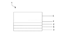
本発明の1つの実施形態における、本発明による電極構造体(Elektrodenanordnung)1が図1に示されており、これは金属または金属酸化物、たとえばMoO3、から成る、第1の中間層3を備える。ここでこの第1の中間層3は、熱的蒸着によってデバイスの有機層上に堆積される。この上にAg等の金属を含む第1の層2が堆積される。この堆積はスパッタリングを用いて行われる。この第1の層2の上に第2の層4が反射防止層として配設される。この第2の層は、たとえばN,N'−ビス(ナフタレン−1−イル)−N,N'−ビス(フェニル)−ベンジジンを含んでいる。
In one embodiment of the invention, an
本発明のもう1つの詳細には示されていない実施形態例においては、本発明による電極構造体1は、金属またはMoO3のような金属酸化物から成る第1の中間層3を備える。ここでこの第1の中間層3は、熱的蒸着によってデバイスの有機層上に堆積される。この上にAg:Ca等の合金を含む第1の層2が堆積される。この堆積はスパッタリングを用いて行われる。この第1の層2の上に第2の層4が反射防止層として配設される。この第2の層は、たとえばN,N'−ビス(ナフタレン−1−イル)−N,N'−ビス(フェニル)−ベンジジンを含んでいる。
In another exemplary embodiment not shown in detail of the invention, the
本発明のもう1つの詳細には示されていない実施形態例においては、本発明による電極構造体1は、アルカリ金属またはCaのようなアルカリ土類金属から成る第1の中間層3を備える。ここでこの第1の中間層3は、熱的蒸着によってデバイスの有機層上に堆積される。この上にAg:Ca等の合金を含む第1の層2が堆積される。この堆積はスパッタリングを用いて行われる。この第1の層2の上に第2の層4が反射防止層として配設される。この第2の層は、たとえばZnS,ZnSe,またはZnTeを含んでいる。
In another exemplary embodiment not shown in detail of the invention, the
本発明のもう1つの詳細には示されていない実施形態例においては、本発明による電極構造体1は、アルカリ金属またはアルカリ土類金属、たとえばMg、から成る第1の中間層3を備える。ここでこの第1の中間層3は、熱的蒸着によってデバイスの有機層上に堆積される。この上にAg:Mg等の合金を含む第1の層2が堆積される。この堆積はスパッタリングを用いて行われる。この第1の層2の上に第2の層4が反射防止層として配設される。この第2の層は、たとえばZnS,ZnSe,またはZnTeを含んでいる。
In an example embodiment not shown in further detail of the invention, the
もう1つの実施形態例においては、電極構造体1の別の構成が図2に示されている。この電極構造体1は上記の実施形態例が備えているものと同様な構造となっているが、第2の層4の上にスクラッチ保護層5が配設されている。このスクラッチ保護層5は、たとえばTiO2で実装されていてよく、150nmの層厚を有する。
In another example embodiment, another configuration of the
もう1つの実施形態例においては、電極構造体1の概略図が図3に示されており、これは金属または金属酸化物、たとえばMoO3、から成る、第1の中間層3を備える。この上にNb2O5から成る、5〜40nmの層厚を有する第2の中間層6が配設されている。この第2の中間層6の上に、Agのような金属から成る上記の第1の層2が堆積されている。ここでこの堆積はスパッタリングによって行われる。この第1の層2の上に第2の層4が反射防止層として配設される。この第2の層は、たとえばN,N'−ビス(ナフタレン−1−イル)−N,N'−ビス(フェニル)−ベンジジンを含んでいる。この第2の層4の上には、スクラッチ保護層5が配設されている。このスクラッチ保護層5は、たとえばTiO2で実装されていてよく、150nmの層厚を有する。
In another example embodiment, a schematic diagram of an
もう1つの詳細には示されていない実施形態例においては、電極構造体1は、金属またはMoO3のような金属酸化物から成る、第1の中間層3を備える。この上にMgから成る、5〜40nmの層厚を有する第2の中間層6が配設されている。この第2の中間層6の上に、Ag:Mgのような合金から成る上記の第1の層2が堆積されている。ここでこの堆積はスパッタリングによって行われる。この第1の層2の上に第2の層4が反射防止層として配設される。この第2の層は、たとえばZnSを含んでいる。この第2の層4の上には、スクラッチ保護層5が配設されている。このスクラッチ保護層5は、たとえばTiO2で実装されていてよく、150nmの層厚を有する。
In another exemplary embodiment not shown in detail, the
もう1つの詳細には示されていない実施形態例においては、電極構造体1は、金属またはMoO3のような金属酸化物から成る、第1の中間層3を備える。この上にCaから成る、5〜40nmの層厚を有する第2の中間層6が配設されている。この第2の中間層6の上に、Ag:Caのような合金から成る、上記の第1の層2が堆積されている。ここでこの堆積はスパッタリングによって行われる。この第1の層2の上に第2の層4が反射防止層として配設される。この第2の層は、たとえばZnSeを含んでいる。この第2の層4の上には、スクラッチ保護層5が配設されている。このスクラッチ保護層5は、たとえばTiO2で実装されていてよく、150nmの層厚を有する。
In another exemplary embodiment not shown in detail, the
上記の実施形態例の詳細に示されていない1つの構成においては、上記の第2の中間層6は、アルミニウムが添加された酸化亜鉛(AZO)で実装されている。ここでこの層厚は5〜40nmである。 In one configuration that is not shown in detail in the above example embodiment, the second intermediate layer 6 is implemented with zinc oxide (AZO) to which aluminum is added. Here, the layer thickness is 5 to 40 nm.
上記の実施形態例の詳細に示されていないもう1つの構成においては、上記の第2の中間層6は、アルミニウムで実装されている。ここでこの層厚は0.2〜3nmである。 In another configuration not shown in detail in the above example embodiment, the second intermediate layer 6 is implemented with aluminum. Here, the layer thickness is 0.2 to 3 nm.
上記の実施形態例の詳細には示されていない1つの構成においては、上記の電極構造体1は、金属またはMoO3のような金属酸化物から成る、第1の中間層3を備える。この上にNb2O5から成る、5〜40nmの層厚を有する第2の中間層6が配設されている。この第2の中間層6の上に、Agのような金属から成る第1の中間層3が堆積されている。ここでこの堆積はスパッタリングによって行われる。この第1の層3の上には、スクラッチ保護層5が配設される。このスクラッチ保護層5は、たとえばTiO2で実装されていてよく、150nmの層厚を有する。
In one configuration not shown in detail in the above example embodiment, the
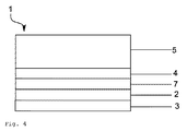
もう1つの実施形態例においては、電極構造体1の概略図が図4に示されており、これは金属または金属酸化物、たとえばMoO3から成る、第1の中間層3を備える。この第1の中間層3の上にNb2O5から成る、5〜40nmの層厚を有する第2の中間層6が配設されている。この上に、Agのような金属から成る第1の層2が配設されている。ここでこの第1の層2の堆積はスパッタリングを用いて行われる。この第1の層2の上に、たとえばITOから成る第3の中間層7が配設されている。ITOから成るこの第3の中間層7の層厚は、5〜40nmである。この第3の中間層7の上に第2の層4が反射防止層として配設される。この第2の層は、たとえばN,N'−ビス(ナフタレン−1−イル)−N,N'−ビス(フェニル)−ベンジジンを含んでいる。この第2の層4の上には、スクラッチ保護層5が配設されている。このスクラッチ保護層5は、たとえばTiO2で実装されていてよく、150nmの層厚を有する。
In another example embodiment, a schematic diagram of an
上記の実施形態例の1つの構成においては、上記の第3の中間層7は、アルミニウム添加された酸化亜鉛AZOで実装されており、この中間層は5〜40nmの層厚を有する。
In one configuration of the above embodiment example, the third
上記の実施形態例の詳細には示されていないもう1つの構成においては、上記の電極構造体1は、金属またはMoO3のような金属酸化物から成る、第1の中間層3を備える。この第1の中間層3の上にNb2O5から成る、5〜40nmの層厚を有する第2の中間層6が配設されている。この上に、Agのような金属から成る第1の層3が配設されている。ここで上記の第1の層2の堆積はスパッタリングを用いて行われる。この第1の中間層2の上に、たとえばITOから成る第3の中間層7が配設されている。ITOから成るこの第3の中間層7の層厚は、5〜40nmである。この第3の層7の上には、スクラッチ保護層5が配設されている。このスクラッチ保護層5は、たとえばTiO2で実装されていてよく、150nmの層厚を有する。
In another configuration not shown in detail in the above embodiment example, the
もう1つの詳細には示されていない実施形態例においては、上記の電極構造体1は、金属またはたとえばMoO3のような金属酸化物から成る、第1の中間層3を備える。この第1の中間層3の上にNb2O5から成る、5〜40nmの層厚を有する第2の中間層6が配設されている。この第2の中間層6の上に、Agのような金属から成る第1の中間層2が配設されている。ここでこの第1の層2の堆積はスパッタリングを用いて行われる。この第1の中間層2の上に、たとえばITOから成る第3の中間層7が配設されている。ITOから成るこの第3の中間層7の層厚は、5〜40nmである。この第3の中間層7の上に第2の層4が反射防止層として配設される。この第2の層は、たとえばN,N'−ビス(ナフタレン−1−イル)−N,N'−ビス(フェニル)−ベンジジンを含んでいる。この第2の層4の上には、スクラッチ保護層5が配設されている。このスクラッチ保護層5は、たとえばTiO2で実装されていてよく、150nmの層厚を有する。
In another exemplary embodiment not shown in detail, the
もう1つの詳細には示されていない実施形態例においては、上記の電極構造体1は、金属またはMoO3のような金属酸化物から成る、第1の中間層3を備える。この第1の中間層3の上にMgから成る、5〜40nmの層厚を有する第2の中間層6が配設されている。この第2の中間層6の上に、Ag:Mgのような合金から成る第1の層2が配設されている。ここでこの第1の層2の堆積はスパッタリングを用いて行われる。この第1の中間層2の上に、たとえばMgから成る第3の中間層7が配設されている。Mgから成るこの第3の中間層7の層厚は、5〜40nmである。この第1の中間層7の上に第3の層4が反射防止層として配設される。この第3の層は、たとえばZnS,ZnSe,またはZnTeを含んでいる。この第2の層4の上には、スクラッチ保護層5が配設されている。このスクラッチ保護層5は、たとえばTiO2で実装されていてよく、150nmの層厚を有する。
In another example embodiment not shown in detail, the
もう1つの詳細には示されていない実施形態例においては、上記の電極構造体1は、金属またはMoO3のような金属酸化物から成る、第1の中間層3を備える。この第1の中間層3の上にNb2O5から成る、5〜40nmの層厚を有する第2の中間層6が配設されている。この第2の中間層6の上に、Agのような金属から成る第1の層2が配設されている。ここでこの第1の層2の堆積はスパッタリングを用いて行われる。この第1の層2の上に、たとえばITOから成る第3の中間層7が配設されている。ITOから成るこの第3の中間層7の層厚は、5〜40nmである。この第3の中間層7の上には、スクラッチ保護層5が配設される。このスクラッチ保護層5は、たとえばTiO2で実装されていてよく、150nmの層厚を有する。
In another example embodiment not shown in detail, the
1 電極構造体
2 第1の層
3 第1の中間層
4 第2の層
5 スクラッチ保護層
6 第2の中間層
7 第3の中間層
DESCRIPTION OF
Claims (14)
前記第1の電極は、前記基板上に配設されており、前記第2の電極は対向電極を形成し、
前記第1の電極と前記第2の電極との間に、少なくとも1つの光活性な層系が配設されており、当該層系は、有機材料を含む少なくとも1つのドナー−アクセプター系を備え、
前記対向電極(1)は、少なくとも1つの第1の層(2)と、当該第1の層(2)と前記有機太陽電池セルの前記光活性な層系との間に配設されている1つの第1の中間層(3)と、当該第1の層(2)上に配設されている1つの第2の層(4)とを備え、前記第1の中間層(3)と前記対向電極の前記第1の層(2)との間に、金属または金属酸化物からなる第2の中間層(6)が挿入されており、当該第2の中間層(6)は、0.05〜30nmの層厚を有し、当該第1の層(2)は、銀、または銀を含む合金を含み、当該第1の中間層(3)はCa,Mg,またはMoOxを含み、当該第2の層(4)は、10〜100nmの層厚および2より大きい屈折率を有し、
前記対向電極(1)と前記光活性な層系の間には、1つの、ドーピングされた輸送層,部分的にドーピングされた輸送層,またはドーピングされていない輸送層が配設されている、
ことを特徴とする有機太陽電池セル。 An organic solar cell on a substrate provided with first and second electrodes,
The first electrode is disposed on the substrate, the second electrode forms a counter electrode,
At least one photoactive layer system is disposed between the first electrode and the second electrode, the layer system comprising at least one donor-acceptor system comprising an organic material,
The counter electrode (1) has at least one first layer (2), is disposed between the photoactive layer system of the first layer and (2) the organic solar cell One first intermediate layer (3) and one second layer (4) disposed on the first layer (2), the first intermediate layer (3) Between the first layer (2) of the counter electrode, a second intermediate layer (6) made of metal or metal oxide is inserted, and the second intermediate layer (6) is zero. has a layer thickness of .05~30Nm, the first layer (2) comprises an alloy comprising silver or silver, the first intermediate layer (3) comprises Ca, Mg, or MoO x, The second layer (4) has a layer thickness of 10 to 100 nm and a refractive index greater than 2,
Between the counter electrode (1) and the photoactive layer system, a doped transport layer, a partially doped transport layer, or an undoped transport layer is disposed.
An organic solar cell characterized by that.
Applications Claiming Priority (5)
| Application Number | Priority Date | Filing Date | Title |
|---|---|---|---|
| DE102012105809.1A DE102012105809B4 (en) | 2012-07-02 | 2012-07-02 | Organic optoelectronic component with transparent counterelectrode and transparent electrode device |
| DE102012105809.1 | 2012-07-02 | ||
| DE102012105810.5A DE102012105810B4 (en) | 2012-07-02 | 2012-07-02 | Transparent electrode for optoelectronic components |
| DE102012105810.5 | 2012-07-02 | ||
| PCT/IB2013/055425 WO2014006565A2 (en) | 2012-07-02 | 2013-07-02 | Transparent electrode for optoelectronic components |
Publications (3)
| Publication Number | Publication Date |
|---|---|
| JP2015527732A JP2015527732A (en) | 2015-09-17 |
| JP2015527732A5 JP2015527732A5 (en) | 2016-08-04 |
| JP6449766B2 true JP6449766B2 (en) | 2019-01-09 |
Family
ID=49223810
Family Applications (1)
| Application Number | Title | Priority Date | Filing Date |
|---|---|---|---|
| JP2015519470A Active JP6449766B2 (en) | 2012-07-02 | 2013-07-02 | Transparent electrodes for optoelectronic devices |
Country Status (8)
| Country | Link |
|---|---|
| US (1) | US11355719B2 (en) |
| EP (1) | EP2867932B1 (en) |
| JP (1) | JP6449766B2 (en) |
| KR (1) | KR102128943B1 (en) |
| CN (1) | CN104584252B (en) |
| BR (1) | BR112014033108B1 (en) |
| ES (1) | ES2762410T3 (en) |
| WO (1) | WO2014006565A2 (en) |
Families Citing this family (7)
| Publication number | Priority date | Publication date | Assignee | Title |
|---|---|---|---|---|
| KR102612902B1 (en) | 2016-04-22 | 2023-12-18 | 삼성디스플레이 주식회사 | Transparent conductive film and electronic device including the same |
| KR102097517B1 (en) | 2016-06-23 | 2020-04-06 | 코오롱인더스트리 주식회사 | Semitransparent organic photovoltaics and method for manufacturing the same |
| KR20170141407A (en) * | 2016-06-15 | 2017-12-26 | 코오롱인더스트리 주식회사 | Organic photovoltaics and method for manufacturing the same |
| KR102113536B1 (en) * | 2017-03-20 | 2020-05-21 | 코오롱인더스트리 주식회사 | Semitransparent organic photovoltaics module |
| CN107068864B (en) * | 2017-04-14 | 2019-05-28 | 武汉华星光电技术有限公司 | The production method of Organic Thin Film Transistors |
| EP3714493A4 (en) * | 2017-11-26 | 2021-09-08 | Ramot at Tel-Aviv University Ltd. | Device and method for neurostimulation |
| DE102019216327A1 (en) * | 2019-10-23 | 2021-04-29 | Fraunhofer-Gesellschaft zur Förderung der angewandten Forschung e.V. | SENSOR WITH A SOLID LAYERED STRUCTURE AND A METHOD FOR MANUFACTURING A SENSOR |
Family Cites Families (45)
| Publication number | Priority date | Publication date | Assignee | Title |
|---|---|---|---|---|
| CA1085947A (en) | 1977-08-02 | 1980-09-16 | Ching W. Tang | Multilayer organic photovoltaic elements |
| US5093698A (en) | 1991-02-12 | 1992-03-03 | Kabushiki Kaisha Toshiba | Organic electroluminescent device |
| JP2538479Y2 (en) * | 1991-11-06 | 1997-06-18 | 三洋電機株式会社 | Photovoltaic device |
| JP3300069B2 (en) * | 1992-11-19 | 2002-07-08 | パイオニア株式会社 | Organic electroluminescence device |
| EP0940860B1 (en) * | 1997-08-27 | 2003-10-15 | Josuke Nakata | Spheric semiconductor device, method for manufacturing the same, and spheric semiconductor device material |
| US6198092B1 (en) * | 1998-08-19 | 2001-03-06 | The Trustees Of Princeton University | Stacked organic photosensitive optoelectronic devices with an electrically parallel configuration |
| DE19905694A1 (en) | 1998-11-27 | 2000-08-17 | Forschungszentrum Juelich Gmbh | Component |
| CN100420058C (en) | 1998-12-17 | 2008-09-17 | 剑桥显示技术有限公司 | Method of production of organic light-emitting devices |
| JP2004119129A (en) * | 2002-09-25 | 2004-04-15 | Tokai Rubber Ind Ltd | Manufacturing method of dye-sensitized solar cell, and dye-sensitized solar cell obtained by it |
| US7675057B2 (en) | 2003-03-19 | 2010-03-09 | Technische Universitaet Dresden | Photoactive component with organic layers |
| US20040211458A1 (en) | 2003-04-28 | 2004-10-28 | General Electric Company | Tandem photovoltaic cell stacks |
| DE10338406A1 (en) | 2003-08-18 | 2005-03-24 | Novaled Gmbh | Doped organic semiconductor materials and process for their preparation |
| US7411223B2 (en) | 2003-09-15 | 2008-08-12 | General Electric Company | Compound electrodes for electronic devices |
| DE10347856B8 (en) | 2003-10-10 | 2006-10-19 | Colorado State University Research Foundation, Fort Collins | Semiconductor doping |
| US7061011B2 (en) | 2003-11-26 | 2006-06-13 | The Trustees Of Princeton University | Bipolar organic devices |
| DE10357044A1 (en) | 2003-12-04 | 2005-07-14 | Novaled Gmbh | Process for doping organic semiconductors with quinonediimine derivatives |
| DE102004010954A1 (en) | 2004-03-03 | 2005-10-06 | Novaled Gmbh | Use of a metal complex as an n-dopant for an organic semiconductive matrix material, organic semiconductor material and electronic component |
| DE102004035965B4 (en) | 2004-07-23 | 2007-07-26 | Novaled Ag | Top-emitting, electroluminescent component with at least one organic layer |
| WO2006041199A1 (en) | 2004-10-13 | 2006-04-20 | Teijin Dupont Films Japan Limited | Multilayer body for dye-sensitized solar cell, electrode for dye-sensitized solar cell and method for producing same |
| JP2008521165A (en) * | 2004-11-16 | 2008-06-19 | インターナショナル・ビジネス・マシーンズ・コーポレーション | Organic light emitting device, method for manufacturing the same, and array comprising a plurality of organic light emitting devices |
| US7259405B2 (en) * | 2004-11-23 | 2007-08-21 | Au Optronics Corporation | Organic photoelectric device with improved electron transport efficiency |
| DE102005010978A1 (en) | 2005-03-04 | 2006-09-07 | Technische Universität Dresden | Photoactive component with organic layers |
| US7825326B2 (en) | 2005-03-21 | 2010-11-02 | Konarka Technologies, Inc. | Polymer photovoltaic cell |
| JP4927423B2 (en) * | 2005-03-24 | 2012-05-09 | エルジー ディスプレイ カンパニー リミテッド | Light emitting device and manufacturing method thereof |
| JP2007035893A (en) * | 2005-07-26 | 2007-02-08 | Matsushita Electric Works Ltd | Organic power generation element |
| US8012530B2 (en) * | 2005-09-06 | 2011-09-06 | Kyoto University | Organic thin-film photoelectric conversion element and method of manufacturing the same |
| US20090199903A1 (en) | 2006-06-30 | 2009-08-13 | Takahito Oyamada | Organic solar cell |
| DE102006053320B4 (en) | 2006-11-13 | 2012-01-19 | Novaled Ag | Use of a coordination compound for doping organic semiconductors |
| DE102006054524B4 (en) | 2006-11-20 | 2022-12-22 | Novaled Gmbh | Use of dithiolene transition metal complexes and selenium-analogous compounds as dopants |
| DE102008051737B4 (en) | 2007-10-24 | 2022-10-06 | Novaled Gmbh | Square-planar transition metal complexes, organic semiconducting materials, and electronic or optoelectronic devices comprising them and use thereof |
| FR2922886B1 (en) | 2007-10-25 | 2010-10-29 | Saint Gobain | GLASS SUBSTRATE COATED WITH LAYERS WITH IMPROVED RESISTIVITY. |
| DE102008011444A1 (en) | 2008-02-27 | 2009-09-10 | Fraunhofer-Gesellschaft zur Förderung der angewandten Forschung e.V. | Thermochrome coated substrates and process for their preparation |
| JP2011524463A (en) * | 2008-05-06 | 2011-09-01 | エージェンシー フォー サイエンス,テクノロジー アンド リサーチ | Conductive structure for light transmissive devices |
| CN102203972A (en) | 2008-10-31 | 2011-09-28 | 巴斯夫欧洲公司 | Merocyanines for producing photoactive layers for organic solar cells and organic photodetectors |
| US8541680B2 (en) * | 2008-12-03 | 2013-09-24 | Applied Materials, Inc. | Photovoltaic cells including peaks and methods of manufacture |
| US20120090679A1 (en) * | 2009-03-17 | 2012-04-19 | Konarka Technologies, Inc. | Metal substrate for a dye sensitized photovoltaic cell |
| JP5357632B2 (en) * | 2009-05-26 | 2013-12-04 | 株式会社カネカ | Photoelectric conversion device |
| KR101704090B1 (en) * | 2009-09-30 | 2017-02-07 | 스미또모 가가꾸 가부시키가이샤 | Laminated structure, polymer, electroluminescent element, and photoelectric conversion element |
| TWI426633B (en) | 2009-12-10 | 2014-02-11 | Univ Nat Chiao Tung | Inverted organic solar cell and method for manufacturing the same |
| US8664518B2 (en) * | 2009-12-11 | 2014-03-04 | Konica Minolta Holdngs, Inc. | Organic photoelectric conversion element and producing method of the same |
| JP2011168747A (en) * | 2010-02-22 | 2011-09-01 | Kyoto Univ | Conjugated polymer, and organic thin film solar cell using the same |
| EP2385556B1 (en) | 2010-05-04 | 2021-01-20 | Heliatek GmbH | Photoactive device with organic layers |
| KR101182447B1 (en) * | 2010-06-16 | 2012-09-12 | 삼성디스플레이 주식회사 | Organic light emitting device and manufacturing method thereof |
| US10121925B2 (en) | 2010-06-18 | 2018-11-06 | University Of Florida Research Foundation, Inc. | Thin film photovoltaic devices with microlens arrays |
| ES2572818T3 (en) | 2010-06-21 | 2016-06-02 | Heliatek Gmbh | Organic solar cell with several transport layer systems |
-
2013
- 2013-07-02 WO PCT/IB2013/055425 patent/WO2014006565A2/en active Application Filing
- 2013-07-02 ES ES13765467T patent/ES2762410T3/en active Active
- 2013-07-02 KR KR1020157002850A patent/KR102128943B1/en active IP Right Grant
- 2013-07-02 CN CN201380035633.XA patent/CN104584252B/en active Active
- 2013-07-02 EP EP13765467.9A patent/EP2867932B1/en active Active
- 2013-07-02 US US14/411,983 patent/US11355719B2/en active Active
- 2013-07-02 JP JP2015519470A patent/JP6449766B2/en active Active
- 2013-07-02 BR BR112014033108-1A patent/BR112014033108B1/en active IP Right Grant
Also Published As
| Publication number | Publication date |
|---|---|
| ES2762410T3 (en) | 2020-05-25 |
| KR102128943B1 (en) | 2020-07-01 |
| CN104584252B (en) | 2018-11-02 |
| WO2014006565A2 (en) | 2014-01-09 |
| KR20150036342A (en) | 2015-04-07 |
| BR112014033108A2 (en) | 2017-06-27 |
| CN104584252A (en) | 2015-04-29 |
| JP2015527732A (en) | 2015-09-17 |
| EP2867932B1 (en) | 2019-09-25 |
| EP2867932A2 (en) | 2015-05-06 |
| BR112014033108B1 (en) | 2020-06-30 |
| US11355719B2 (en) | 2022-06-07 |
| WO2014006565A3 (en) | 2014-07-03 |
| US20150295195A1 (en) | 2015-10-15 |
Similar Documents
| Publication | Publication Date | Title |
|---|---|---|
| JP6310014B2 (en) | Photoactive components containing organic layers | |
| JP6449766B2 (en) | Transparent electrodes for optoelectronic devices | |
| AU2004221377B2 (en) | Photoactive component comprising organic layers | |
| US9112163B2 (en) | Photoactive component having a plurality of transport layer systems | |
| US9070888B2 (en) | Photoelectronic device and image sensor | |
| ES2879526T3 (en) | Photoactive component with reversed layer order and procedure for its production | |
| US10756284B2 (en) | Photoactive component having organic layers | |
| US9431621B2 (en) | Metal oxide charge transport material doped with organic molecules | |
| US20150228916A1 (en) | Bottom-up ultra-thin functional optoelectronic films and devices | |
| JP5881116B2 (en) | Organic photoelectric conversion element and organic thin film solar cell | |
| Meiss et al. | Efficient semitransparent small-molecule organic solar cells | |
| JP2011233692A (en) | Photoelectric converter, organic solar cell and photoelectric conversion apparatus using these | |
| Osasa et al. | Determination of photo-active region in organic thin film solar cells with an organic heterojunction | |
| DE102012105810A1 (en) | Optoelectronic component e.g. solar cell, has counter electrode that is provided with main layer and interlayer, and photoactive layer system which is provided between counter electrode and main electrodes | |
| Kubo | pn-Homojunction Organic Solar Cells | |
| 久保雅之 et al. | pn-Homojunction Organic Solar Cells |
Legal Events
| Date | Code | Title | Description |
|---|---|---|---|
| A521 | Request for written amendment filed |
Free format text: JAPANESE INTERMEDIATE CODE: A523 Effective date: 20160608 |
|
| A621 | Written request for application examination |
Free format text: JAPANESE INTERMEDIATE CODE: A621 Effective date: 20160608 |
|
| A977 | Report on retrieval |
Free format text: JAPANESE INTERMEDIATE CODE: A971007 Effective date: 20170317 |
|
| A131 | Notification of reasons for refusal |
Free format text: JAPANESE INTERMEDIATE CODE: A131 Effective date: 20170329 |
|
| A601 | Written request for extension of time |
Free format text: JAPANESE INTERMEDIATE CODE: A601 Effective date: 20170628 |
|
| A601 | Written request for extension of time |
Free format text: JAPANESE INTERMEDIATE CODE: A601 Effective date: 20170828 |
|
| A521 | Request for written amendment filed |
Free format text: JAPANESE INTERMEDIATE CODE: A523 Effective date: 20170913 |
|
| A131 | Notification of reasons for refusal |
Free format text: JAPANESE INTERMEDIATE CODE: A131 Effective date: 20180214 |
|
| A601 | Written request for extension of time |
Free format text: JAPANESE INTERMEDIATE CODE: A601 Effective date: 20180510 |
|
| A601 | Written request for extension of time |
Free format text: JAPANESE INTERMEDIATE CODE: A601 Effective date: 20180713 |
|
| A521 | Request for written amendment filed |
Free format text: JAPANESE INTERMEDIATE CODE: A523 Effective date: 20180813 |
|
| TRDD | Decision of grant or rejection written | ||
| A01 | Written decision to grant a patent or to grant a registration (utility model) |
Free format text: JAPANESE INTERMEDIATE CODE: A01 Effective date: 20181107 |
|
| A61 | First payment of annual fees (during grant procedure) |
Free format text: JAPANESE INTERMEDIATE CODE: A61 Effective date: 20181206 |
|
| R150 | Certificate of patent or registration of utility model |
Ref document number: 6449766 Country of ref document: JP Free format text: JAPANESE INTERMEDIATE CODE: R150 |
|
| R250 | Receipt of annual fees |
Free format text: JAPANESE INTERMEDIATE CODE: R250 |
|
| R250 | Receipt of annual fees |
Free format text: JAPANESE INTERMEDIATE CODE: R250 |
|
| R250 | Receipt of annual fees |
Free format text: JAPANESE INTERMEDIATE CODE: R250 |