JP6431200B2 - サーマルヘッドおよびサーマルプリンタ - Google Patents
サーマルヘッドおよびサーマルプリンタ Download PDFInfo
- Publication number
- JP6431200B2 JP6431200B2 JP2017531087A JP2017531087A JP6431200B2 JP 6431200 B2 JP6431200 B2 JP 6431200B2 JP 2017531087 A JP2017531087 A JP 2017531087A JP 2017531087 A JP2017531087 A JP 2017531087A JP 6431200 B2 JP6431200 B2 JP 6431200B2
- Authority
- JP
- Japan
- Prior art keywords
- layer
- inorganic particles
- interface
- conductive layer
- protective layer
- Prior art date
- Legal status (The legal status is an assumption and is not a legal conclusion. Google has not performed a legal analysis and makes no representation as to the accuracy of the status listed.)
- Active
Links
- 239000010410 layer Substances 0.000 claims description 188
- 239000010954 inorganic particle Substances 0.000 claims description 122
- 239000011247 coating layer Substances 0.000 claims description 77
- 239000011241 protective layer Substances 0.000 claims description 53
- 239000000758 substrate Substances 0.000 claims description 42
- 239000000463 material Substances 0.000 claims description 19
- 229920005989 resin Polymers 0.000 claims description 15
- 239000011347 resin Substances 0.000 claims description 15
- 239000002245 particle Substances 0.000 claims description 11
- 229910010272 inorganic material Inorganic materials 0.000 claims description 8
- 239000011147 inorganic material Substances 0.000 claims description 8
- 230000007723 transport mechanism Effects 0.000 claims description 6
- 238000010438 heat treatment Methods 0.000 claims description 4
- 238000007789 sealing Methods 0.000 description 17
- 238000005338 heat storage Methods 0.000 description 13
- 238000000034 method Methods 0.000 description 12
- 239000000853 adhesive Substances 0.000 description 8
- 230000001070 adhesive effect Effects 0.000 description 8
- 238000004544 sputter deposition Methods 0.000 description 8
- 239000010408 film Substances 0.000 description 7
- 238000007639 printing Methods 0.000 description 7
- 238000007650 screen-printing Methods 0.000 description 6
- 238000010586 diagram Methods 0.000 description 5
- 239000010409 thin film Substances 0.000 description 5
- 230000032258 transport Effects 0.000 description 5
- 239000011521 glass Substances 0.000 description 3
- 229910052751 metal Inorganic materials 0.000 description 3
- 239000002184 metal Substances 0.000 description 3
- XEEYBQQBJWHFJM-UHFFFAOYSA-N Iron Chemical compound [Fe] XEEYBQQBJWHFJM-UHFFFAOYSA-N 0.000 description 2
- 239000005062 Polybutadiene Substances 0.000 description 2
- 229910004541 SiN Inorganic materials 0.000 description 2
- 229910004298 SiO 2 Inorganic materials 0.000 description 2
- 229910052799 carbon Inorganic materials 0.000 description 2
- 238000005260 corrosion Methods 0.000 description 2
- 230000007797 corrosion Effects 0.000 description 2
- 238000005520 cutting process Methods 0.000 description 2
- 239000003822 epoxy resin Substances 0.000 description 2
- 238000007733 ion plating Methods 0.000 description 2
- 238000005304 joining Methods 0.000 description 2
- 230000000873 masking effect Effects 0.000 description 2
- 238000007750 plasma spraying Methods 0.000 description 2
- 229920002857 polybutadiene Polymers 0.000 description 2
- 229920000647 polyepoxide Polymers 0.000 description 2
- 229910052814 silicon oxide Inorganic materials 0.000 description 2
- 229920002050 silicone resin Polymers 0.000 description 2
- 239000010935 stainless steel Substances 0.000 description 2
- 229910001220 stainless steel Inorganic materials 0.000 description 2
- PNEYBMLMFCGWSK-UHFFFAOYSA-N Alumina Chemical compound [O-2].[O-2].[O-2].[Al+3].[Al+3] PNEYBMLMFCGWSK-UHFFFAOYSA-N 0.000 description 1
- OKTJSMMVPCPJKN-UHFFFAOYSA-N Carbon Chemical compound [C] OKTJSMMVPCPJKN-UHFFFAOYSA-N 0.000 description 1
- RYGMFSIKBFXOCR-UHFFFAOYSA-N Copper Chemical compound [Cu] RYGMFSIKBFXOCR-UHFFFAOYSA-N 0.000 description 1
- 239000004593 Epoxy Substances 0.000 description 1
- ATJFFYVFTNAWJD-UHFFFAOYSA-N Tin Chemical compound [Sn] ATJFFYVFTNAWJD-UHFFFAOYSA-N 0.000 description 1
- 229910045601 alloy Inorganic materials 0.000 description 1
- 239000000956 alloy Substances 0.000 description 1
- 229910052782 aluminium Inorganic materials 0.000 description 1
- XAGFODPZIPBFFR-UHFFFAOYSA-N aluminium Chemical compound [Al] XAGFODPZIPBFFR-UHFFFAOYSA-N 0.000 description 1
- 230000015572 biosynthetic process Effects 0.000 description 1
- 239000000919 ceramic Substances 0.000 description 1
- 229910052802 copper Inorganic materials 0.000 description 1
- 239000010949 copper Substances 0.000 description 1
- 239000006185 dispersion Substances 0.000 description 1
- 239000012777 electrically insulating material Substances 0.000 description 1
- 230000005611 electricity Effects 0.000 description 1
- 229910052737 gold Inorganic materials 0.000 description 1
- 230000020169 heat generation Effects 0.000 description 1
- 229910052742 iron Inorganic materials 0.000 description 1
- 239000007769 metal material Substances 0.000 description 1
- 229910003465 moissanite Inorganic materials 0.000 description 1
- 229910021421 monocrystalline silicon Inorganic materials 0.000 description 1
- 229910052759 nickel Inorganic materials 0.000 description 1
- 229910052757 nitrogen Inorganic materials 0.000 description 1
- 239000011368 organic material Substances 0.000 description 1
- 239000003960 organic solvent Substances 0.000 description 1
- 230000001590 oxidative effect Effects 0.000 description 1
- 238000000059 patterning Methods 0.000 description 1
- 238000001259 photo etching Methods 0.000 description 1
- 238000007747 plating Methods 0.000 description 1
- 229920001721 polyimide Polymers 0.000 description 1
- 239000009719 polyimide resin Substances 0.000 description 1
- 239000000843 powder Substances 0.000 description 1
- 238000003825 pressing Methods 0.000 description 1
- 230000008569 process Effects 0.000 description 1
- 230000004044 response Effects 0.000 description 1
- 239000004065 semiconductor Substances 0.000 description 1
- 229910052710 silicon Inorganic materials 0.000 description 1
- 229910010271 silicon carbide Inorganic materials 0.000 description 1
- 229910000679 solder Inorganic materials 0.000 description 1
- 238000005507 spraying Methods 0.000 description 1
- 230000003068 static effect Effects 0.000 description 1
- 238000003860 storage Methods 0.000 description 1
- 238000007751 thermal spraying Methods 0.000 description 1
- 229920001187 thermosetting polymer Polymers 0.000 description 1
- 229910052719 titanium Inorganic materials 0.000 description 1
Images


Classifications
-
- B—PERFORMING OPERATIONS; TRANSPORTING
- B41—PRINTING; LINING MACHINES; TYPEWRITERS; STAMPS
- B41J—TYPEWRITERS; SELECTIVE PRINTING MECHANISMS, i.e. MECHANISMS PRINTING OTHERWISE THAN FROM A FORME; CORRECTION OF TYPOGRAPHICAL ERRORS
- B41J2/00—Typewriters or selective printing mechanisms characterised by the printing or marking process for which they are designed
- B41J2/315—Typewriters or selective printing mechanisms characterised by the printing or marking process for which they are designed characterised by selective application of heat to a heat sensitive printing or impression-transfer material
- B41J2/32—Typewriters or selective printing mechanisms characterised by the printing or marking process for which they are designed characterised by selective application of heat to a heat sensitive printing or impression-transfer material using thermal heads
- B41J2/335—Structure of thermal heads
- B41J2/33505—Constructional details
- B41J2/3353—Protective layers
-
- B—PERFORMING OPERATIONS; TRANSPORTING
- B41—PRINTING; LINING MACHINES; TYPEWRITERS; STAMPS
- B41J—TYPEWRITERS; SELECTIVE PRINTING MECHANISMS, i.e. MECHANISMS PRINTING OTHERWISE THAN FROM A FORME; CORRECTION OF TYPOGRAPHICAL ERRORS
- B41J2/00—Typewriters or selective printing mechanisms characterised by the printing or marking process for which they are designed
- B41J2/315—Typewriters or selective printing mechanisms characterised by the printing or marking process for which they are designed characterised by selective application of heat to a heat sensitive printing or impression-transfer material
- B41J2/32—Typewriters or selective printing mechanisms characterised by the printing or marking process for which they are designed characterised by selective application of heat to a heat sensitive printing or impression-transfer material using thermal heads
- B41J2/335—Structure of thermal heads
- B41J2/33505—Constructional details
- B41J2/3351—Electrode layers
-
- B—PERFORMING OPERATIONS; TRANSPORTING
- B41—PRINTING; LINING MACHINES; TYPEWRITERS; STAMPS
- B41J—TYPEWRITERS; SELECTIVE PRINTING MECHANISMS, i.e. MECHANISMS PRINTING OTHERWISE THAN FROM A FORME; CORRECTION OF TYPOGRAPHICAL ERRORS
- B41J2/00—Typewriters or selective printing mechanisms characterised by the printing or marking process for which they are designed
- B41J2/315—Typewriters or selective printing mechanisms characterised by the printing or marking process for which they are designed characterised by selective application of heat to a heat sensitive printing or impression-transfer material
- B41J2/32—Typewriters or selective printing mechanisms characterised by the printing or marking process for which they are designed characterised by selective application of heat to a heat sensitive printing or impression-transfer material using thermal heads
- B41J2/335—Structure of thermal heads
- B41J2/33505—Constructional details
- B41J2/33515—Heater layers
-
- B—PERFORMING OPERATIONS; TRANSPORTING
- B41—PRINTING; LINING MACHINES; TYPEWRITERS; STAMPS
- B41J—TYPEWRITERS; SELECTIVE PRINTING MECHANISMS, i.e. MECHANISMS PRINTING OTHERWISE THAN FROM A FORME; CORRECTION OF TYPOGRAPHICAL ERRORS
- B41J2/00—Typewriters or selective printing mechanisms characterised by the printing or marking process for which they are designed
- B41J2/315—Typewriters or selective printing mechanisms characterised by the printing or marking process for which they are designed characterised by selective application of heat to a heat sensitive printing or impression-transfer material
- B41J2/32—Typewriters or selective printing mechanisms characterised by the printing or marking process for which they are designed characterised by selective application of heat to a heat sensitive printing or impression-transfer material using thermal heads
- B41J2/335—Structure of thermal heads
- B41J2/33505—Constructional details
- B41J2/33525—Passivation layers
-
- B—PERFORMING OPERATIONS; TRANSPORTING
- B41—PRINTING; LINING MACHINES; TYPEWRITERS; STAMPS
- B41J—TYPEWRITERS; SELECTIVE PRINTING MECHANISMS, i.e. MECHANISMS PRINTING OTHERWISE THAN FROM A FORME; CORRECTION OF TYPOGRAPHICAL ERRORS
- B41J2/00—Typewriters or selective printing mechanisms characterised by the printing or marking process for which they are designed
- B41J2/315—Typewriters or selective printing mechanisms characterised by the printing or marking process for which they are designed characterised by selective application of heat to a heat sensitive printing or impression-transfer material
- B41J2/32—Typewriters or selective printing mechanisms characterised by the printing or marking process for which they are designed characterised by selective application of heat to a heat sensitive printing or impression-transfer material using thermal heads
- B41J2/335—Structure of thermal heads
- B41J2/33505—Constructional details
- B41J2/33535—Substrates
-
- B—PERFORMING OPERATIONS; TRANSPORTING
- B41—PRINTING; LINING MACHINES; TYPEWRITERS; STAMPS
- B41J—TYPEWRITERS; SELECTIVE PRINTING MECHANISMS, i.e. MECHANISMS PRINTING OTHERWISE THAN FROM A FORME; CORRECTION OF TYPOGRAPHICAL ERRORS
- B41J2/00—Typewriters or selective printing mechanisms characterised by the printing or marking process for which they are designed
- B41J2/315—Typewriters or selective printing mechanisms characterised by the printing or marking process for which they are designed characterised by selective application of heat to a heat sensitive printing or impression-transfer material
- B41J2/32—Typewriters or selective printing mechanisms characterised by the printing or marking process for which they are designed characterised by selective application of heat to a heat sensitive printing or impression-transfer material using thermal heads
- B41J2/335—Structure of thermal heads
- B41J2/3354—Structure of thermal heads characterised by geometry
-
- B—PERFORMING OPERATIONS; TRANSPORTING
- B41—PRINTING; LINING MACHINES; TYPEWRITERS; STAMPS
- B41J—TYPEWRITERS; SELECTIVE PRINTING MECHANISMS, i.e. MECHANISMS PRINTING OTHERWISE THAN FROM A FORME; CORRECTION OF TYPOGRAPHICAL ERRORS
- B41J2/00—Typewriters or selective printing mechanisms characterised by the printing or marking process for which they are designed
- B41J2/315—Typewriters or selective printing mechanisms characterised by the printing or marking process for which they are designed characterised by selective application of heat to a heat sensitive printing or impression-transfer material
- B41J2/32—Typewriters or selective printing mechanisms characterised by the printing or marking process for which they are designed characterised by selective application of heat to a heat sensitive printing or impression-transfer material using thermal heads
- B41J2/335—Structure of thermal heads
- B41J2/3355—Structure of thermal heads characterised by materials
-
- B—PERFORMING OPERATIONS; TRANSPORTING
- B41—PRINTING; LINING MACHINES; TYPEWRITERS; STAMPS
- B41J—TYPEWRITERS; SELECTIVE PRINTING MECHANISMS, i.e. MECHANISMS PRINTING OTHERWISE THAN FROM A FORME; CORRECTION OF TYPOGRAPHICAL ERRORS
- B41J2/00—Typewriters or selective printing mechanisms characterised by the printing or marking process for which they are designed
- B41J2/315—Typewriters or selective printing mechanisms characterised by the printing or marking process for which they are designed characterised by selective application of heat to a heat sensitive printing or impression-transfer material
- B41J2/32—Typewriters or selective printing mechanisms characterised by the printing or marking process for which they are designed characterised by selective application of heat to a heat sensitive printing or impression-transfer material using thermal heads
- B41J2/335—Structure of thermal heads
- B41J2/33555—Structure of thermal heads characterised by type
- B41J2/3357—Surface type resistors
-
- B—PERFORMING OPERATIONS; TRANSPORTING
- B41—PRINTING; LINING MACHINES; TYPEWRITERS; STAMPS
- B41J—TYPEWRITERS; SELECTIVE PRINTING MECHANISMS, i.e. MECHANISMS PRINTING OTHERWISE THAN FROM A FORME; CORRECTION OF TYPOGRAPHICAL ERRORS
- B41J2/00—Typewriters or selective printing mechanisms characterised by the printing or marking process for which they are designed
- B41J2/315—Typewriters or selective printing mechanisms characterised by the printing or marking process for which they are designed characterised by selective application of heat to a heat sensitive printing or impression-transfer material
- B41J2/32—Typewriters or selective printing mechanisms characterised by the printing or marking process for which they are designed characterised by selective application of heat to a heat sensitive printing or impression-transfer material using thermal heads
- B41J2/335—Structure of thermal heads
- B41J2/3359—Manufacturing processes
-
- B—PERFORMING OPERATIONS; TRANSPORTING
- B41—PRINTING; LINING MACHINES; TYPEWRITERS; STAMPS
- B41J—TYPEWRITERS; SELECTIVE PRINTING MECHANISMS, i.e. MECHANISMS PRINTING OTHERWISE THAN FROM A FORME; CORRECTION OF TYPOGRAPHICAL ERRORS
- B41J2/00—Typewriters or selective printing mechanisms characterised by the printing or marking process for which they are designed
- B41J2/315—Typewriters or selective printing mechanisms characterised by the printing or marking process for which they are designed characterised by selective application of heat to a heat sensitive printing or impression-transfer material
- B41J2/32—Typewriters or selective printing mechanisms characterised by the printing or marking process for which they are designed characterised by selective application of heat to a heat sensitive printing or impression-transfer material using thermal heads
- B41J2/35—Typewriters or selective printing mechanisms characterised by the printing or marking process for which they are designed characterised by selective application of heat to a heat sensitive printing or impression-transfer material using thermal heads providing current or voltage to the thermal head
- B41J2/355—Control circuits for heating-element selection
Landscapes
- Engineering & Computer Science (AREA)
- Manufacturing & Machinery (AREA)
- Physics & Mathematics (AREA)
- Geometry (AREA)
- Electronic Switches (AREA)
Description
(例えば、特許文献1参照)。
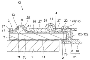
以下、サーマルヘッドX1について図1〜5を参照して説明する。図1は、サーマルヘッドX1の構成を概略的に示している。図2は、保護層25、被覆層27、および封止部材12を一点鎖線にて示している。
図7を用いてサーマルヘッドX2について説明する。なお、サーマルヘッドX1と同一の部材については同じ符号を付しており、以下同様とする。サーマルヘッドX2は、無機粒子116が、サーマルヘッドX1の無機粒子16と異なっている。
図8,9を用いてサーマルヘッドX3について説明する。サーマルヘッドX3は、第1無機粒子216と第2無機粒子26とを有している。
図10を用いてサーマルヘッドX4について説明する。なお、図10(a)に示すH1は、無機粒子316cの導電層25bからの突出高さを示している。また、図10(b)に示すH2は、無機粒子316aの導電層25bからの突出高さを示している。また、図10(a)に示すE1は第1領域を示しており、図10(a)に示すE2は第2領域を示している。
Z1 サーマルプリンタ
E1 第1領域
E2 第2領域
1 放熱板
3 ヘッド基体
7 基板
9 発熱部
13 蓄熱層
14 接着部材
16,116,216,316 無機粒子
16a1,16b1 第1部位
16a2,16b2 第2部位
216b3 第3部位
316a4,316b4 第4部位
18a 表面
18b 側面
18c 第3界面
18d 第4界面
20 界面
20a1,20b1 第1界面
20a2,20b2 第2界面
22,24,30 領域
25 保護層
25a 絶縁層
25b 導電層
26 第2無機粒子
27 被覆層
31 コネクタ
Claims (8)
- 基板と、
前記基板上に設けられた発熱部と、
前記基板上に設けられ、前記発熱部と電気的に接続された電極と、
前記発熱部、および前記電極の一部を覆い、無機材料により形成された保護層と、
前記保護層上に設けられ、樹脂材料により形成された被覆層と、
前記保護層の表面に、前記表面から突出した無機粒子と、を備え、
前記無機粒子は、前記被覆層の内部に位置する第1部位と、前記保護層の内部に位置する第2部位とを有しており、
前記無機粒子は、前記第1部位と前記被覆層との界面である第1界面と、前記第2部位と前記保護層との界面である第2界面と、を有しており、
断面視して、前記第1界面の長さが前記第2界面の長さよりも長いことを特徴とするサーマルヘッド。 - 基板と、
前記基板上に設けられた発熱部と、
前記基板上に設けられ、前記発熱部と電気的に接続された電極と、
前記発熱部、および前記電極の一部を覆い、無機材料により形成された保護層と、
前記保護層上に設けられ、樹脂材料により形成された被覆層と、
前記保護層の表面に、前記表面から突出した無機粒子と、を備え、
前記無機粒子は、前記被覆層の内部に位置する第1部位と、前記保護層の内部に位置する第2部位とを有しており、
前記保護層と前記被覆層との界面である第3界面を有しており、
断面視して、前記無機粒子は、前記第1部位に最大径を有する部位が位置していることを特徴とするサーマルヘッド。 - 前記第1部位は、前記第3界面から離れる方向にさらに突出した突出部を有する、請求項2に記載のサーマルヘッド。
- 前記保護層は、前記発熱部および前記電極上に設けられた絶縁層と、前記絶縁層上に設けられた導電層とを有しており、
断面視して、前記絶縁層の幅が、前記導電層の幅よりも広い、請求項1〜3のいずれか一項に記載のサーマルヘッド。 - 前記導電層は、表面および側面が前記被覆層で被覆されており、
前記無機粒子は、前記導電層の前記側面に、前記側面から突出して設けられており、
前記被覆層を形成する樹脂材料が、前記無機粒子の前記第1部位と前記絶縁層との間に入り込んでいる、請求項4に記載のサーマルヘッド。 - 基板と、
前記基板上に設けられた発熱部と、
前記基板上に設けられ、前記発熱部と電気的に接続された電極と、
前記発熱部、および前記電極の一部を覆い、無機材料により形成された保護層と、
前記保護層上に設けられ、樹脂材料により形成された被覆層と、
前記保護層の表面に、前記表面から突出した無機粒子と、を備え、
前記無機粒子は、前記被覆層の内部に位置する第1部位と、前記保護層の内部に位置する第2部位とを有しており、
前記保護層は、前記発熱部および前記電極上に設けられた絶縁層と、前記絶縁層上に設けられた導電層とを有しており、
断面視して、前記絶縁層の幅が、前記導電層の幅よりも広く、
前記無機粒子の前記第2部位は、前記絶縁層の内部に位置している第3部位を有していることを特徴とするサーマルヘッド。 - 前記無機粒子は、第1無機粒子と、前記第1無機粒子よりも平均粒径の小さい第2無機粒子とを有する、請求項1〜6のいずれか一項に記載のサーマルヘッド。
- 請求項1〜7のうちいずれか一項に記載のサーマルヘッドと、
前記発熱部上に記録媒体を搬送する搬送機構と、
前記発熱部上に前記記録媒体を押圧するプラテンローラと、を備えることを特徴とするサーマルプリンタ。
Applications Claiming Priority (3)
| Application Number | Priority Date | Filing Date | Title |
|---|---|---|---|
| JP2015149733 | 2015-07-29 | ||
| JP2015149733 | 2015-07-29 | ||
| PCT/JP2016/068671 WO2017018106A1 (ja) | 2015-07-29 | 2016-06-23 | サーマルヘッドおよびサーマルプリンタ |
Publications (2)
| Publication Number | Publication Date |
|---|---|
| JPWO2017018106A1 JPWO2017018106A1 (ja) | 2018-04-26 |
| JP6431200B2 true JP6431200B2 (ja) | 2018-11-28 |
Family
ID=57884486
Family Applications (1)
| Application Number | Title | Priority Date | Filing Date |
|---|---|---|---|
| JP2017531087A Active JP6431200B2 (ja) | 2015-07-29 | 2016-06-23 | サーマルヘッドおよびサーマルプリンタ |
Country Status (4)
| Country | Link |
|---|---|
| US (1) | US10144224B2 (ja) |
| JP (1) | JP6431200B2 (ja) |
| CN (1) | CN107848311B (ja) |
| WO (1) | WO2017018106A1 (ja) |
Families Citing this family (4)
| Publication number | Priority date | Publication date | Assignee | Title |
|---|---|---|---|---|
| JP6987588B2 (ja) * | 2017-09-29 | 2022-01-05 | 京セラ株式会社 | サーマルヘッド及びサーマルプリンタ |
| JP7128901B2 (ja) * | 2018-09-27 | 2022-08-31 | 京セラ株式会社 | サーマルプリンタ |
| JP7245684B2 (ja) * | 2019-03-19 | 2023-03-24 | ローム株式会社 | サーマルプリントヘッド及びサーマルプリントヘッドの製造方法 |
| JP7336588B2 (ja) * | 2020-03-31 | 2023-08-31 | 京セラ株式会社 | サーマルヘッドおよびサーマルプリンタ |
Family Cites Families (7)
| Publication number | Priority date | Publication date | Assignee | Title |
|---|---|---|---|---|
| JP2535864B2 (ja) | 1987-02-05 | 1996-09-18 | 三菱電機株式会社 | サ−マルヘツド |
| JPH01128849A (ja) | 1987-11-16 | 1989-05-22 | Hitachi Ltd | 厚膜型感熱記録ヘッド |
| JP3117753B2 (ja) | 1991-09-03 | 2000-12-18 | ローム株式会社 | サーマルプリントヘッドの構造 |
| JP2006181822A (ja) * | 2004-12-27 | 2006-07-13 | Toshiba Hokuto Electronics Corp | サーマルプリントヘッドおよびその製造方法 |
| JP5094639B2 (ja) | 2008-08-28 | 2012-12-12 | 京セラ株式会社 | 記録ヘッドおよびこれを備える記録装置 |
| JP5825778B2 (ja) * | 2010-12-10 | 2015-12-02 | ローム株式会社 | サーマルプリントヘッド |
| JP2014144623A (ja) | 2013-01-30 | 2014-08-14 | Kyocera Corp | サーマルヘッドおよびサーマルプリンタ |
-
2016
- 2016-06-23 CN CN201680042323.4A patent/CN107848311B/zh active Active
- 2016-06-23 US US15/748,088 patent/US10144224B2/en active Active
- 2016-06-23 WO PCT/JP2016/068671 patent/WO2017018106A1/ja active Application Filing
- 2016-06-23 JP JP2017531087A patent/JP6431200B2/ja active Active
Also Published As
| Publication number | Publication date |
|---|---|
| WO2017018106A1 (ja) | 2017-02-02 |
| US20180207951A1 (en) | 2018-07-26 |
| JPWO2017018106A1 (ja) | 2018-04-26 |
| US10144224B2 (en) | 2018-12-04 |
| CN107848311B (zh) | 2019-08-16 |
| CN107848311A (zh) | 2018-03-27 |
Similar Documents
| Publication | Publication Date | Title |
|---|---|---|
| JP6431200B2 (ja) | サーマルヘッドおよびサーマルプリンタ | |
| JP6196417B1 (ja) | サーマルヘッドおよびサーマルプリンタ | |
| JP6059412B1 (ja) | サーマルヘッドおよびサーマルプリンタ | |
| JP6096997B2 (ja) | サーマルヘッドおよびサーマルプリンタ | |
| JP6419006B2 (ja) | サーマルヘッドおよびサーマルプリンタ | |
| WO2017018415A1 (ja) | サーマルヘッドおよびサーマルプリンタ | |
| JP6767296B2 (ja) | サーマルヘッドおよびサーマルプリンタ | |
| JP6050562B2 (ja) | サーマルヘッドおよびサーマルプリンタ | |
| JP6046872B2 (ja) | サーマルヘッドおよびサーマルプリンタ | |
| WO2017057364A1 (ja) | サーマルヘッドおよびサーマルプリンタ | |
| JP6582060B2 (ja) | サーマルヘッドおよびサーマルプリンタ | |
| JP6154334B2 (ja) | サーマルヘッドおよびサーマルプリンタ | |
| JP2014141050A (ja) | サーマルヘッドおよびこれを備えるサーマルプリンタ | |
| JP6901419B2 (ja) | サーマルヘッドおよびサーマルプリンタ | |
| WO2020196078A1 (ja) | サーマルヘッドおよびサーマルプリンタ | |
| JP6130618B1 (ja) | サーマルヘッドおよびサーマルプリンタ | |
| JP6725402B2 (ja) | サーマルヘッドおよびサーマルプリンタ | |
| JP2018034371A (ja) | サーマルヘッドおよびサーマルプリンタ | |
| JP2017043013A (ja) | サーマルヘッドおよびサーマルプリンタ | |
| JP6352799B2 (ja) | サーマルヘッドおよびサーマルプリンタ | |
| JP6426541B2 (ja) | サーマルヘッドおよびサーマルプリンタ | |
| JP6110198B2 (ja) | サーマルヘッドおよびサーマルプリンタ | |
| JP2015182240A (ja) | サーマルヘッドおよびサーマルプリンタ | |
| JP2014027222A (ja) | 接続構造、およびこの接続構造を備えるサーマルプリンタ | |
| JP2017043076A (ja) | サーマルヘッドおよびサーマルプリンタ |
Legal Events
| Date | Code | Title | Description |
|---|---|---|---|
| A621 | Written request for application examination |
Free format text: JAPANESE INTERMEDIATE CODE: A621 Effective date: 20180117 |
|
| A131 | Notification of reasons for refusal |
Free format text: JAPANESE INTERMEDIATE CODE: A131 Effective date: 20180807 |
|
| A521 | Request for written amendment filed |
Free format text: JAPANESE INTERMEDIATE CODE: A523 Effective date: 20180912 |
|
| TRDD | Decision of grant or rejection written | ||
| A01 | Written decision to grant a patent or to grant a registration (utility model) |
Free format text: JAPANESE INTERMEDIATE CODE: A01 Effective date: 20181002 |
|
| A61 | First payment of annual fees (during grant procedure) |
Free format text: JAPANESE INTERMEDIATE CODE: A61 Effective date: 20181101 |
|
| R150 | Certificate of patent or registration of utility model |
Ref document number: 6431200 Country of ref document: JP Free format text: JAPANESE INTERMEDIATE CODE: R150 |