JP6431200B2 - Thermal head and thermal printer - Google Patents
Thermal head and thermal printer Download PDFInfo
- Publication number
- JP6431200B2 JP6431200B2 JP2017531087A JP2017531087A JP6431200B2 JP 6431200 B2 JP6431200 B2 JP 6431200B2 JP 2017531087 A JP2017531087 A JP 2017531087A JP 2017531087 A JP2017531087 A JP 2017531087A JP 6431200 B2 JP6431200 B2 JP 6431200B2
- Authority
- JP
- Japan
- Prior art keywords
- layer
- inorganic particles
- interface
- conductive layer
- protective layer
- Prior art date
- Legal status (The legal status is an assumption and is not a legal conclusion. Google has not performed a legal analysis and makes no representation as to the accuracy of the status listed.)
- Active
Links
- 239000010410 layer Substances 0.000 claims description 188
- 239000010954 inorganic particle Substances 0.000 claims description 122
- 239000011247 coating layer Substances 0.000 claims description 77
- 239000011241 protective layer Substances 0.000 claims description 53
- 239000000758 substrate Substances 0.000 claims description 42
- 239000000463 material Substances 0.000 claims description 19
- 229920005989 resin Polymers 0.000 claims description 15
- 239000011347 resin Substances 0.000 claims description 15
- 239000002245 particle Substances 0.000 claims description 11
- 229910010272 inorganic material Inorganic materials 0.000 claims description 8
- 239000011147 inorganic material Substances 0.000 claims description 8
- 230000007723 transport mechanism Effects 0.000 claims description 6
- 238000010438 heat treatment Methods 0.000 claims description 4
- 238000007789 sealing Methods 0.000 description 17
- 238000005338 heat storage Methods 0.000 description 13
- 238000000034 method Methods 0.000 description 12
- 239000000853 adhesive Substances 0.000 description 8
- 230000001070 adhesive effect Effects 0.000 description 8
- 238000004544 sputter deposition Methods 0.000 description 8
- 239000010408 film Substances 0.000 description 7
- 238000007639 printing Methods 0.000 description 7
- 238000007650 screen-printing Methods 0.000 description 6
- 238000010586 diagram Methods 0.000 description 5
- 239000010409 thin film Substances 0.000 description 5
- 230000032258 transport Effects 0.000 description 5
- 239000011521 glass Substances 0.000 description 3
- 229910052751 metal Inorganic materials 0.000 description 3
- 239000002184 metal Substances 0.000 description 3
- XEEYBQQBJWHFJM-UHFFFAOYSA-N Iron Chemical compound [Fe] XEEYBQQBJWHFJM-UHFFFAOYSA-N 0.000 description 2
- 239000005062 Polybutadiene Substances 0.000 description 2
- 229910004541 SiN Inorganic materials 0.000 description 2
- 229910004298 SiO 2 Inorganic materials 0.000 description 2
- 229910052799 carbon Inorganic materials 0.000 description 2
- 238000005260 corrosion Methods 0.000 description 2
- 230000007797 corrosion Effects 0.000 description 2
- 238000005520 cutting process Methods 0.000 description 2
- 239000003822 epoxy resin Substances 0.000 description 2
- 238000007733 ion plating Methods 0.000 description 2
- 238000005304 joining Methods 0.000 description 2
- 230000000873 masking effect Effects 0.000 description 2
- 238000007750 plasma spraying Methods 0.000 description 2
- 229920002857 polybutadiene Polymers 0.000 description 2
- 229920000647 polyepoxide Polymers 0.000 description 2
- 229910052814 silicon oxide Inorganic materials 0.000 description 2
- 229920002050 silicone resin Polymers 0.000 description 2
- 239000010935 stainless steel Substances 0.000 description 2
- 229910001220 stainless steel Inorganic materials 0.000 description 2
- PNEYBMLMFCGWSK-UHFFFAOYSA-N Alumina Chemical compound [O-2].[O-2].[O-2].[Al+3].[Al+3] PNEYBMLMFCGWSK-UHFFFAOYSA-N 0.000 description 1
- OKTJSMMVPCPJKN-UHFFFAOYSA-N Carbon Chemical compound [C] OKTJSMMVPCPJKN-UHFFFAOYSA-N 0.000 description 1
- RYGMFSIKBFXOCR-UHFFFAOYSA-N Copper Chemical compound [Cu] RYGMFSIKBFXOCR-UHFFFAOYSA-N 0.000 description 1
- 239000004593 Epoxy Substances 0.000 description 1
- ATJFFYVFTNAWJD-UHFFFAOYSA-N Tin Chemical compound [Sn] ATJFFYVFTNAWJD-UHFFFAOYSA-N 0.000 description 1
- 229910045601 alloy Inorganic materials 0.000 description 1
- 239000000956 alloy Substances 0.000 description 1
- 229910052782 aluminium Inorganic materials 0.000 description 1
- XAGFODPZIPBFFR-UHFFFAOYSA-N aluminium Chemical compound [Al] XAGFODPZIPBFFR-UHFFFAOYSA-N 0.000 description 1
- 230000015572 biosynthetic process Effects 0.000 description 1
- 239000000919 ceramic Substances 0.000 description 1
- 229910052802 copper Inorganic materials 0.000 description 1
- 239000010949 copper Substances 0.000 description 1
- 239000006185 dispersion Substances 0.000 description 1
- 239000012777 electrically insulating material Substances 0.000 description 1
- 230000005611 electricity Effects 0.000 description 1
- 229910052737 gold Inorganic materials 0.000 description 1
- 230000020169 heat generation Effects 0.000 description 1
- 229910052742 iron Inorganic materials 0.000 description 1
- 239000007769 metal material Substances 0.000 description 1
- 229910003465 moissanite Inorganic materials 0.000 description 1
- 229910021421 monocrystalline silicon Inorganic materials 0.000 description 1
- 229910052759 nickel Inorganic materials 0.000 description 1
- 229910052757 nitrogen Inorganic materials 0.000 description 1
- 239000011368 organic material Substances 0.000 description 1
- 239000003960 organic solvent Substances 0.000 description 1
- 230000001590 oxidative effect Effects 0.000 description 1
- 238000000059 patterning Methods 0.000 description 1
- 238000001259 photo etching Methods 0.000 description 1
- 238000007747 plating Methods 0.000 description 1
- 229920001721 polyimide Polymers 0.000 description 1
- 239000009719 polyimide resin Substances 0.000 description 1
- 239000000843 powder Substances 0.000 description 1
- 238000003825 pressing Methods 0.000 description 1
- 230000008569 process Effects 0.000 description 1
- 230000004044 response Effects 0.000 description 1
- 239000004065 semiconductor Substances 0.000 description 1
- 229910052710 silicon Inorganic materials 0.000 description 1
- 229910010271 silicon carbide Inorganic materials 0.000 description 1
- 229910000679 solder Inorganic materials 0.000 description 1
- 238000005507 spraying Methods 0.000 description 1
- 230000003068 static effect Effects 0.000 description 1
- 238000003860 storage Methods 0.000 description 1
- 238000007751 thermal spraying Methods 0.000 description 1
- 229920001187 thermosetting polymer Polymers 0.000 description 1
- 229910052719 titanium Inorganic materials 0.000 description 1
Images


Classifications
-
- B—PERFORMING OPERATIONS; TRANSPORTING
- B41—PRINTING; LINING MACHINES; TYPEWRITERS; STAMPS
- B41J—TYPEWRITERS; SELECTIVE PRINTING MECHANISMS, i.e. MECHANISMS PRINTING OTHERWISE THAN FROM A FORME; CORRECTION OF TYPOGRAPHICAL ERRORS
- B41J2/00—Typewriters or selective printing mechanisms characterised by the printing or marking process for which they are designed
- B41J2/315—Typewriters or selective printing mechanisms characterised by the printing or marking process for which they are designed characterised by selective application of heat to a heat sensitive printing or impression-transfer material
- B41J2/32—Typewriters or selective printing mechanisms characterised by the printing or marking process for which they are designed characterised by selective application of heat to a heat sensitive printing or impression-transfer material using thermal heads
- B41J2/335—Structure of thermal heads
- B41J2/33505—Constructional details
- B41J2/3353—Protective layers
-
- B—PERFORMING OPERATIONS; TRANSPORTING
- B41—PRINTING; LINING MACHINES; TYPEWRITERS; STAMPS
- B41J—TYPEWRITERS; SELECTIVE PRINTING MECHANISMS, i.e. MECHANISMS PRINTING OTHERWISE THAN FROM A FORME; CORRECTION OF TYPOGRAPHICAL ERRORS
- B41J2/00—Typewriters or selective printing mechanisms characterised by the printing or marking process for which they are designed
- B41J2/315—Typewriters or selective printing mechanisms characterised by the printing or marking process for which they are designed characterised by selective application of heat to a heat sensitive printing or impression-transfer material
- B41J2/32—Typewriters or selective printing mechanisms characterised by the printing or marking process for which they are designed characterised by selective application of heat to a heat sensitive printing or impression-transfer material using thermal heads
- B41J2/335—Structure of thermal heads
- B41J2/33505—Constructional details
- B41J2/3351—Electrode layers
-
- B—PERFORMING OPERATIONS; TRANSPORTING
- B41—PRINTING; LINING MACHINES; TYPEWRITERS; STAMPS
- B41J—TYPEWRITERS; SELECTIVE PRINTING MECHANISMS, i.e. MECHANISMS PRINTING OTHERWISE THAN FROM A FORME; CORRECTION OF TYPOGRAPHICAL ERRORS
- B41J2/00—Typewriters or selective printing mechanisms characterised by the printing or marking process for which they are designed
- B41J2/315—Typewriters or selective printing mechanisms characterised by the printing or marking process for which they are designed characterised by selective application of heat to a heat sensitive printing or impression-transfer material
- B41J2/32—Typewriters or selective printing mechanisms characterised by the printing or marking process for which they are designed characterised by selective application of heat to a heat sensitive printing or impression-transfer material using thermal heads
- B41J2/335—Structure of thermal heads
- B41J2/33505—Constructional details
- B41J2/33515—Heater layers
-
- B—PERFORMING OPERATIONS; TRANSPORTING
- B41—PRINTING; LINING MACHINES; TYPEWRITERS; STAMPS
- B41J—TYPEWRITERS; SELECTIVE PRINTING MECHANISMS, i.e. MECHANISMS PRINTING OTHERWISE THAN FROM A FORME; CORRECTION OF TYPOGRAPHICAL ERRORS
- B41J2/00—Typewriters or selective printing mechanisms characterised by the printing or marking process for which they are designed
- B41J2/315—Typewriters or selective printing mechanisms characterised by the printing or marking process for which they are designed characterised by selective application of heat to a heat sensitive printing or impression-transfer material
- B41J2/32—Typewriters or selective printing mechanisms characterised by the printing or marking process for which they are designed characterised by selective application of heat to a heat sensitive printing or impression-transfer material using thermal heads
- B41J2/335—Structure of thermal heads
- B41J2/33505—Constructional details
- B41J2/33525—Passivation layers
-
- B—PERFORMING OPERATIONS; TRANSPORTING
- B41—PRINTING; LINING MACHINES; TYPEWRITERS; STAMPS
- B41J—TYPEWRITERS; SELECTIVE PRINTING MECHANISMS, i.e. MECHANISMS PRINTING OTHERWISE THAN FROM A FORME; CORRECTION OF TYPOGRAPHICAL ERRORS
- B41J2/00—Typewriters or selective printing mechanisms characterised by the printing or marking process for which they are designed
- B41J2/315—Typewriters or selective printing mechanisms characterised by the printing or marking process for which they are designed characterised by selective application of heat to a heat sensitive printing or impression-transfer material
- B41J2/32—Typewriters or selective printing mechanisms characterised by the printing or marking process for which they are designed characterised by selective application of heat to a heat sensitive printing or impression-transfer material using thermal heads
- B41J2/335—Structure of thermal heads
- B41J2/33505—Constructional details
- B41J2/33535—Substrates
-
- B—PERFORMING OPERATIONS; TRANSPORTING
- B41—PRINTING; LINING MACHINES; TYPEWRITERS; STAMPS
- B41J—TYPEWRITERS; SELECTIVE PRINTING MECHANISMS, i.e. MECHANISMS PRINTING OTHERWISE THAN FROM A FORME; CORRECTION OF TYPOGRAPHICAL ERRORS
- B41J2/00—Typewriters or selective printing mechanisms characterised by the printing or marking process for which they are designed
- B41J2/315—Typewriters or selective printing mechanisms characterised by the printing or marking process for which they are designed characterised by selective application of heat to a heat sensitive printing or impression-transfer material
- B41J2/32—Typewriters or selective printing mechanisms characterised by the printing or marking process for which they are designed characterised by selective application of heat to a heat sensitive printing or impression-transfer material using thermal heads
- B41J2/335—Structure of thermal heads
- B41J2/3354—Structure of thermal heads characterised by geometry
-
- B—PERFORMING OPERATIONS; TRANSPORTING
- B41—PRINTING; LINING MACHINES; TYPEWRITERS; STAMPS
- B41J—TYPEWRITERS; SELECTIVE PRINTING MECHANISMS, i.e. MECHANISMS PRINTING OTHERWISE THAN FROM A FORME; CORRECTION OF TYPOGRAPHICAL ERRORS
- B41J2/00—Typewriters or selective printing mechanisms characterised by the printing or marking process for which they are designed
- B41J2/315—Typewriters or selective printing mechanisms characterised by the printing or marking process for which they are designed characterised by selective application of heat to a heat sensitive printing or impression-transfer material
- B41J2/32—Typewriters or selective printing mechanisms characterised by the printing or marking process for which they are designed characterised by selective application of heat to a heat sensitive printing or impression-transfer material using thermal heads
- B41J2/335—Structure of thermal heads
- B41J2/3355—Structure of thermal heads characterised by materials
-
- B—PERFORMING OPERATIONS; TRANSPORTING
- B41—PRINTING; LINING MACHINES; TYPEWRITERS; STAMPS
- B41J—TYPEWRITERS; SELECTIVE PRINTING MECHANISMS, i.e. MECHANISMS PRINTING OTHERWISE THAN FROM A FORME; CORRECTION OF TYPOGRAPHICAL ERRORS
- B41J2/00—Typewriters or selective printing mechanisms characterised by the printing or marking process for which they are designed
- B41J2/315—Typewriters or selective printing mechanisms characterised by the printing or marking process for which they are designed characterised by selective application of heat to a heat sensitive printing or impression-transfer material
- B41J2/32—Typewriters or selective printing mechanisms characterised by the printing or marking process for which they are designed characterised by selective application of heat to a heat sensitive printing or impression-transfer material using thermal heads
- B41J2/335—Structure of thermal heads
- B41J2/33555—Structure of thermal heads characterised by type
- B41J2/3357—Surface type resistors
-
- B—PERFORMING OPERATIONS; TRANSPORTING
- B41—PRINTING; LINING MACHINES; TYPEWRITERS; STAMPS
- B41J—TYPEWRITERS; SELECTIVE PRINTING MECHANISMS, i.e. MECHANISMS PRINTING OTHERWISE THAN FROM A FORME; CORRECTION OF TYPOGRAPHICAL ERRORS
- B41J2/00—Typewriters or selective printing mechanisms characterised by the printing or marking process for which they are designed
- B41J2/315—Typewriters or selective printing mechanisms characterised by the printing or marking process for which they are designed characterised by selective application of heat to a heat sensitive printing or impression-transfer material
- B41J2/32—Typewriters or selective printing mechanisms characterised by the printing or marking process for which they are designed characterised by selective application of heat to a heat sensitive printing or impression-transfer material using thermal heads
- B41J2/335—Structure of thermal heads
- B41J2/3359—Manufacturing processes
-
- B—PERFORMING OPERATIONS; TRANSPORTING
- B41—PRINTING; LINING MACHINES; TYPEWRITERS; STAMPS
- B41J—TYPEWRITERS; SELECTIVE PRINTING MECHANISMS, i.e. MECHANISMS PRINTING OTHERWISE THAN FROM A FORME; CORRECTION OF TYPOGRAPHICAL ERRORS
- B41J2/00—Typewriters or selective printing mechanisms characterised by the printing or marking process for which they are designed
- B41J2/315—Typewriters or selective printing mechanisms characterised by the printing or marking process for which they are designed characterised by selective application of heat to a heat sensitive printing or impression-transfer material
- B41J2/32—Typewriters or selective printing mechanisms characterised by the printing or marking process for which they are designed characterised by selective application of heat to a heat sensitive printing or impression-transfer material using thermal heads
- B41J2/35—Typewriters or selective printing mechanisms characterised by the printing or marking process for which they are designed characterised by selective application of heat to a heat sensitive printing or impression-transfer material using thermal heads providing current or voltage to the thermal head
- B41J2/355—Control circuits for heating-element selection
Landscapes
- Engineering & Computer Science (AREA)
- Manufacturing & Machinery (AREA)
- Physics & Mathematics (AREA)
- Geometry (AREA)
- Electronic Switches (AREA)
Description
本発明は、サーマルヘッドおよびサーマルプリンタに関する。 The present invention relates to a thermal head and a thermal printer.
従来、ファクシミリあるいはビデオプリンタ等の印画デバイスとして、種々のサーマルヘッドが提案されている。例えば、基板と、基板上に設けられた発熱部と、基板上に設けられ、発熱部と電気的に接続された電極と、発熱部、および電極の一部を覆う保護層とを備えたサーマルヘッドが知られている。このサーマルヘッドにおいて、保護層は、無機材料により形成されており、保護層上に樹脂材料により形成された被覆層が設けられている
(例えば、特許文献1参照)。Conventionally, various thermal heads have been proposed as printing devices such as facsimiles and video printers. For example, a thermal device that includes a substrate, a heat generating portion provided on the substrate, an electrode provided on the substrate and electrically connected to the heat generating portion, and a protective layer that covers the heat generating portion and a part of the electrode. The head is known. In this thermal head, the protective layer is formed of an inorganic material, and a coating layer formed of a resin material is provided on the protective layer (see, for example, Patent Document 1).
本開示のサーマルヘッドは、基板と、前記基板上に設けられた発熱部と、前記基板上に設けられ、前記発熱部と電気的に接続された電極と、前記発熱部、および前記電極の一部を覆い、無機材料により形成された保護層と、前記保護層上に設けられ、樹脂材料により形成された被覆層と、前記保護層の表面に、前記表面から突出して設けられた無機粒子とを備える。また、前記無機粒子は、前記被覆層の内部に位置する第1部位と、前記保護層の内部に位置する第2部位とを有する。 A thermal head according to the present disclosure includes a substrate, a heat generating portion provided on the substrate, an electrode provided on the substrate and electrically connected to the heat generating portion, the heat generating portion, and one of the electrodes. A protective layer formed of an inorganic material, covering the part, a coating layer provided on the protective layer and formed of a resin material, and inorganic particles provided on the surface of the protective layer so as to protrude from the surface Is provided. Moreover, the said inorganic particle has the 1st site | part located inside the said coating layer, and the 2nd site | part located inside the said protective layer.
本開示のサーマルプリンタは、上記に記載のサーマルヘッドと、前記発熱部上に記録媒体を搬送する搬送機構と、前記発熱部上に前記記録媒体を押圧するプラテンローラとを備える。 A thermal printer according to the present disclosure includes the thermal head described above, a transport mechanism that transports a recording medium onto the heat generating unit, and a platen roller that presses the recording medium onto the heat generating unit.
<第1の実施形態>
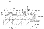
以下、サーマルヘッドX1について図1〜5を参照して説明する。図1は、サーマルヘッドX1の構成を概略的に示している。図2は、保護層25、被覆層27、および封止部材12を一点鎖線にて示している。<First Embodiment>
Hereinafter, the thermal head X1 will be described with reference to FIGS. FIG. 1 schematically shows the configuration of the thermal head X1. FIG. 2 shows the
サーマルヘッドX1は、ヘッド基体3と、コネクタ31と、封止部材12と、放熱板1と、接着部材14とを備えている。サーマルヘッドX1は、放熱板1上に接着部材14を介してヘッド基体3が載置されている。ヘッド基体3は、外部からの電圧が印加することにより発熱部9を発熱させ記録媒体(不図示)に印画を行っている。コネクタ31は、外部とヘッド基体3とを電気的に接続している。封止部材12は、コネクタ31とヘッド基体3とを接合している。放熱板1は、ヘッド基体3の熱を放熱するために設けられている。接着部材14は、ヘッド基体3と放熱板1とを接着している。
The thermal head X1 includes a
放熱板1は、直方体形状をなしている。放熱板1は、例えば、銅、鉄またはアルミニウム等の金属材料で形成されており、ヘッド基体3の発熱部9で発生した熱のうち、印画に寄与しない熱を放熱する機能を有している。
The
ヘッド基体3は、図1に示すように、平面視して、長方形状に形成されており、ヘッド基体3の基板7上にサーマルヘッドX1を構成する各部材が設けられている。ヘッド基体3は、外部より供給された電気信号に従い、記録媒体(不図示)に印字を行う機能を有する。
As shown in FIG. 1, the
図1〜3を用いて、ヘッド基体3を構成する各部材について説明する。
Each member which comprises the head base |
基板7は、放熱板1上に配置されており、平面視して、矩形状をなしている。そのため、基板7は、第1長辺7aと、第2長辺7bと、第1短辺7cと、第2短辺7dと、側面7eと、第1面7fと、第2面7gとを有している。側面7eはコネクタ31側に設けられている。第1面7f上にヘッド基体3を構成する各部材が設けられている。第2面7gは、放熱板1側に設けられている。基板7は、例えば、アルミナセラミックス等の電気絶縁性材料あるいは単結晶シリコン等の半導体材料等によって形成されている。
The board |
基板7の第1面7f上に蓄熱層13が設けられている。蓄熱層13は、基板7の上方へ向けて突出して隆起している。蓄熱層13は、主走査方向に沿って延び、断面が略半楕円形状をなしている。また、蓄熱層13は、印画する記録媒体P(図5参照)を、発熱部9上に形成された保護層25に良好に押し当てるように機能している。蓄熱層13は、基板7からの高さが15〜90μmで設けられている。
A
蓄熱層13は、熱伝導性の低いガラスで形成されており、発熱部9で発生する熱の一部を一時的に蓄積する。そのため、発熱部9の温度を上昇させるのに要する時間を短くすることができ、サーマルヘッドX1の熱応答特性を高めるように機能する。蓄熱層13は、例えば、ガラス粉末に適当な有機溶剤を混合して得た所定のガラスペーストを従来周知のスクリーン印刷等によって基板7の上面に塗布し、これを焼成することで形成される。
The
電気抵抗層15は、基板7上、および蓄熱層13上に設けられており、電気抵抗層15上に、ヘッド基体3を構成する各種電極が設けられている。電気抵抗層15は、ヘッド基体3を構成する各種電極と同形状にパターニングされており、共通電極17と個別電極19との間に電気抵抗層15が露出した露出領域を有する。各露出領域は発熱部9を構成しており、蓄熱層13上に所定の間隔をおいて列状に配置されている。なお、電気抵抗層15は、共通電極17と個別電極19との間にのみに設けられていてもよい。
The
複数の発熱部9は、説明の便宜上、図2では簡略化して記載しているが、例えば、100dpi〜2400dpi(dot per inch)等の密度で配置される。電気抵抗層15は、例えば、TaN系、TaSiO系、TaSiNO系、TiSiO系、TiSiCO系またはNbSiO系等の電気抵抗値の高い材料によって形成されている。そのため、発熱部9に電圧が印加されたときに、ジュール発熱によって発熱部9が発熱する。
The plurality of
共通電極17は、主配線部17a,17dと、副配線部17bと、リード部17cとを備えている。共通電極17は、複数の発熱部9と、コネクタ31とを電気的に接続している。主配線部17aは、基板7の第1長辺7aに沿って延びている。副配線部17bは、基板7の第1短辺7cおよび第2短辺7dのそれぞれに沿って延びている。リード部17cは、主配線部17aから各発熱部9に向かって個別に延びている。主配線部17dは、基板7の第2長辺7bに沿って延びている。
The
複数の個別電極19は、発熱部9と駆動IC11との間を電気的に接続している。また、個別電極19は、複数の発熱部9を複数の群に分けており、各群の発熱部9と各群に対応して設けられた駆動IC11とを電気的に接続している。
The plurality of
複数のIC−コネクタ接続電極21は、駆動IC11とコネクタ31との間を電気的に接続している。各駆動IC11に接続された複数のIC−コネクタ接続電極21は、異なる機能を有する複数の配線で構成されている。
The plurality of IC-
グランド電極4は、個別電極19と、IC−コネクタ接続電極21と、共通電極17の主配線部17dとにより取り囲まれるように配置されている。グランド電極4は、0〜1Vのグランド電位に保持されている。
The
接続端子2は、共通電極17、個別電極19、IC−コネクタ接続電極21およびグランド電極4をコネクタ31に接続するために、基板7の第2長辺7b側に設けられている。接続端子2はコネクタピン8に対応して設けられている。コネクタ31に接続する際は、コネクタピン8がそれぞれ電気的に独立するように、コネクタピン8と接続端子2とが接続されている。
The
複数のIC−IC接続電極32は、隣り合う駆動IC11を電気的に接続している。複数のIC−IC接続電極32は、それぞれIC−コネクタ接続電極21に対応するように設けられており、各種信号を隣り合う駆動IC11に伝えている。
The plurality of IC-IC connection electrodes 32 electrically connect
上記のヘッド基体3を構成する各種電極は、例えば、以下の方法で作製できる。各々を構成する材料層を蓄熱層13上に、例えばスパッタリング法等の薄膜成形技術によって順次積層する。次に、積層体を従来周知のフォトエッチング等を用いて所定のパターンに加工することにより形成される。なお、ヘッド基体3を構成する各種電極は、同じ工程によって同時に形成することができる。
The various electrodes constituting the
駆動IC11は、図2に示すように、複数の発熱部9の各群に対応して配置されているとともに、個別電極19の他端部とIC−コネクタ接続電極21の一端部とに接続されている。駆動IC11は、各発熱部9の通電状態を制御する機能を有している。駆動IC11としては、内部に複数のスイッチング素子を有する切替部材を用いればよい。
As shown in FIG. 2, the
駆動IC11は、個別電極19、IC−IC接続電極32およびIC−コネクタ接続電極21に接続された状態で、エポキシ樹脂、あるいはシリコーン樹脂等の樹脂からなるハードコート29によって封止されている。
The
基板7の第1面7fに設けられた蓄熱層13上には、発熱部9、共通電極17の一部および個別電極19の一部を被覆する保護層25が形成されている。
On the
保護層25は、発熱部9、共通電極17および個別電極19の被覆した領域を、大気中に含まれている水分等の付着による腐食、あるいは印画する記録媒体との接触による摩耗から保護するためのものである。保護層25は、SiN、SiO2、SiON、SiC、あるいはダイヤモンドライクカーボン等の無機材料を用いて形成することができる。The
保護層25は、スパッタリング法等の薄膜形成技術あるいはスクリーン印刷等の厚膜形成技術を用いて作製することができる。
The
基板7上には、共通電極17、個別電極19およびIC−コネクタ接続電極21を部分的に被覆する被覆層27が設けられている。被覆層27は、共通電極17、個別電極19、IC−IC接続電極32およびIC−コネクタ接続電極21の被覆した領域を、大気との接触による酸化、あるいは大気中に含まれている水分等の付着による腐食から保護するためのものである。被覆層27は、エポキシ系樹脂、ポリイミド系樹脂、あるいはシリコーン系樹脂等の樹脂材料により形成することができる。
On the
コネクタ31とヘッド基体3とは、コネクタピン8、導電部材23、および封止部材12により固定されている。導電部材23は、接続端子2とコネクタピン8との間に配置されており、例えば、はんだ、あるいは異方性導電接着剤等を例示することができる。なお、導電部材23は、必ずしも設けられなくてもよく、接続端子2との間にNi、Au、あるいはPdによるめっき層(不図示)を設けてもよい。
The
コネクタ31は、複数のコネクタピン8と、複数のコネクタピン8を収納するハウジング10とを有している。複数のコネクタピン8は、一方がハウジング10の外部に露出しており、他方がハウジング10の内部に収容されている。複数のコネクタピン8は、ヘッド基体3の接続端子2に電気的に接続されており、ヘッド基体3の各種電極と電気的に接続されている。
The
封止部材12は、第1封止部材12aと第2封止部材12bとを有している。第1封止部材12aは基板7の第1面7f上に位置しており、第2封止部材12bは基板7の第2面7g上に位置している。第1封止部材12aは、コネクタピン8と各種電極とを封止するように設けられており、第2封止部材12bは、コネクタピン8と基板7との接触部を封止するように設けられている。
The sealing
封止部材12は、接続端子2、およびコネクタピン8が外部に露出しないように設けられており、例えば、エポキシ系の熱硬化性の樹脂、紫外線硬化性の樹脂、あるいは可視光硬化性の樹脂により形成することができる。なお、第1封止部材12aと第2封止部材12bとが同じ材料により形成されていてもよく、別の材料により形成されていてもよい。
The sealing
接着部材14は、放熱板1上に配置されており、ヘッド基体3の第2面7gと放熱板1とを接合している。接着部材14としては、両面テープ、あるいは樹脂性の接着剤を例示することができる。
The
図4,5を用いて、保護層25、被覆層27および無機粒子16について詳細に説明する。なお、図5では被覆層27(図4参照)の図示を省略している。
The
保護層25は、絶縁層25aと導電層25bとを有している。絶縁層25aは、発熱部9上と、共通電極17の一部の上と、個別電極19の一部の上とに設けられている。
The
絶縁層25aは、比抵抗の大きな材料により形成されており、例えば、SiO2、SiN、あるいはSiONにより形成することができる。絶縁層25aの厚みは、例えば、0.1〜10μmとすることができる。絶縁層25aを設けることにより、主走査方向に複数配列された発熱部9同士を絶縁することができる。絶縁層25aは、例えば、スクリーン印刷法、スパッタリング法、あるいはイオンプレーティング法により形成することができる。The insulating
導電層25bは、絶縁層25aよりも比抵抗の小さな材料により形成されており、例えば、TiN、TiCN、あるいはTaSiOにより形成することができる。導電層25bは、表面18aと、側面18bとを有している。
The
導電層25bの厚みは、例えば、2〜15μmとすることができる。導電層25bを設けることにより、保護層25と記録媒体P(図6参照)との接触により生じた静電気を除電することができる。導電層25bは、例えば、スクリーン印刷法、スパッタリング法、あるいはイオンプレーティング法により形成することができる。
The thickness of the
無機粒子16は、保護層25の表面18aまたは側面18bに設けられている。無機粒子16aは、導電層25bの表面18aから被覆層27に向けて突出している。無機粒子16bは、導電層25bの側面18bから被覆層27に向けて突出している。無機粒子16は、粒径が5〜300μmであり、金属、合金、あるいはセラミックにより形成することができる。無機粒子16は、導電層25bを形成する材料と同一の材料により形成されると導電層25bの内部に応力が生じ難い。具体的には、Ti,C,N,Siの元素により形成されると導電層25bの内部に応力が生じ難くなる。
The
無機粒子16aは、導電層25bの表面18aから被覆層27に向けて突出している。無機粒子16aは、被覆層27の内部に位置する第1部位16a1と、導電層25bの内部に位置する第2部位16a2とを有している。言い換えると、無機粒子16aは、導電層25bの表面18aに位置しており、第2部位16a2が導電層25b内に埋設されている。
The
無機粒子16aは、被覆層27および導電層25bと界面20aを介して接触している。界面20aは、第1界面20a1と第2界面20a2とを有している。第1界面20a1は、第1部位16a1と被覆層27との界面である。第2界面20a2は、第2部位16a2と導電層25bとの界面である。
The
無機粒子16bは、導電層25bの側面18bから被覆層27に向けて突出している。無機粒子16bは、被覆層27の内部に位置する第1部位16b1と、導電層25bの内部に位置する第2部位16b2とを有している。言い換えると、無機粒子16bは、導電層25bの側面18bに位置しており、第2部位16b2が導電層25bに埋設されている。そして、第1部位16b1と絶縁層25aとの間に領域22が形成されている。
The
無機粒子16bは、被覆層27および導電層25bと界面20bを介して接触している。界面20bは、第1界面20b1と第2界面20b2とを有している。第1界面20b1は、第1部位16b1と被覆層27との界面である。第2界面20b2は、第2部位16b2と導電層25bとの界面である。
The
ここで、保護層25は、無機材料により形成されている。保護層25上に設けられた被覆層27は、有機材料により形成されている。このため、保護層25と被覆層27との接合力が弱く、被覆層27が保護層25から剥離するおそれがある。
Here, the
無機粒子16aは、導電層25bの表面18aに、表面18aから突出して設けられており、第1部位16a1と第2部位16a2とを有している。そのため、被覆層27と接触した第1部位16a1が被覆層27に接合されるとともに、第2部位16a2が導電層25bの内部に位置することとなり、無機粒子16aにより導電層25bと被覆層27との接合力を向上させることができる。
The
すなわち、被覆層27を形成する樹脂材料は、導電層25b上に設けられた際に、無機粒子16aの第1部位16a1の表面を回り込むように塗布される。それにより、第1部位16a1と被覆層27との接合力を向上させることができる。そして、第2部位16a2は、導電層25bの内部に埋設されているため、被覆層27に外力が生じた場合においても、第2部位16a2が導電層25b内に留まることができ、無機粒子16aが導電層25bから剥離しにくくなる。その結果、導電層25bと被覆層27との接合力を向上させることができる。
That is, the resin material forming the
図4に示すように、断面視して、絶縁層25aの幅が、導電層25bの幅よりも広くなっている。それにより、導電層25bが、発熱部9、共通電極17、および個別電極19と接触して短絡を生じる可能性を低減することができる。絶縁層25aの幅は、導電層25bの幅の1.1〜1.5倍であると、短絡が生じる可能性を低減することができる。なお、断面視とは、サーマルヘッドX1を副走査方向に沿って切断した切断面を確認することである。
As shown in FIG. 4, the width of the insulating
無機粒子16bは、導電層25bの側面18bに、側面18bから突出して設けられており、第1部位16b1と第2部位16b2とを有している。そして、第1部位16b1と絶縁層25aとの間に領域22が生じている。そして、被覆層27を形成する樹脂材料が、第1部位16b1と絶縁層25aとの間の領域22に入り込んでいる。
The
そのため、被覆層27が、第1部位16b1を回り込むように領域22に位置することとなる。その結果、被覆層27に外力が生じた場合においても、領域22に配置された被覆層27が、外力に対して第1部位16b1に引っ掛かるように作用する。それゆえ、被覆層27が導電層25bから剥離し難くなる。
Therefore, the
保護層25は、例えば、以下の方法により形成することができる。
The
各種電極がパターニングされた基板7に、マスキングを行い、絶縁層25aをスパッタリング法により形成する。次に、絶縁層25aを形成した時よりも、マスキングの開口を小さくし、スパッタリング法により導電層25bを形成する。
Masking is performed on the
導電層25bをスパッタリング法により形成した後に、例えば、無機粒子16をプラズマ溶射、あるいはアーク溶射等をすることにより、導電層25b中に無機粒子16を含有させることができる。また、例えば、溶射により導電層25bに無機粒子16を含有させることから、導電層25bの中にランダムに分散させることができる。このように、例えば、スパッタリング法とプラズマ溶射を繰り返すことにより、無機粒子16を含有する導電層25bを作製することができる。
After the
そして、被覆層27を作製するために、樹脂をスクリーン印刷法により、導電層25b上に塗布、硬化してサーマルヘッドX1を作製することができる。このように、導電層25bを薄膜形成技術により形成した場合、導電層25bの膜応力が高く、被覆層27との接合力が小さくなるが、導電層25bが無機粒子16を含有することにより、導電層25bと被覆層27との接合力を向上させることができる。
And in order to produce the
また、導電層25bをスクリーン印刷法により形成する場合には、絶縁層25aが設けられた基板7に、所定の印刷マスクを介して導電層25bを印刷する。次に、無機粒子16をランダムに散布し、乾燥させる。続いて、無機粒子16を含有する保護層25を焼成することにより、導電層25bを作成することができる。なお、導電層25bの印刷、無機粒子16の散布、導電層25bを繰り返すことにより、無機粒子16a,16bを含有する導電層25bを作製することができる。
When the
なお、保護層25が絶縁層25aと導電層25bとを備えた例を示したが、必ずしも絶縁層25aと導電層25bとを備えていなくてもよい。すなわち、単層の保護層25としてもよい。また、絶縁層25aまたは導電層25bを多層化してもよい。
Note that although the
次に、サーマルプリンタZ1について、図6を参照しつつ説明する。 Next, the thermal printer Z1 will be described with reference to FIG.
本実施形態のサーマルプリンタZ1は、上述のサーマルヘッドX1と、搬送機構40と、プラテンローラ50と、電源装置60と、制御装置70とを備えている。サーマルヘッドX1は、サーマルプリンタZ1の筐体(不図示)に設けられた取付部材80の取付面80aに取り付けられている。なお、サーマルヘッドX1は、後述する記録媒体Pの搬送方向Sに直交する方向である主走査方向に沿うようにして、取付部材80に取り付けられている。
The thermal printer Z1 of this embodiment includes the above-described thermal head X1, the
搬送機構40は、駆動部(不図示)と、搬送ローラ43,45,47,49とを有している。搬送機構40は、感熱紙、インクが転写される受像紙等の記録媒体Pを図6の矢印S方向に搬送して、サーマルヘッドX1の複数の発熱部9上に位置する保護層25上に搬送するためのものである。駆動部は、搬送ローラ43,45,47,49を駆動させる機能を有しており、例えば、モータを用いることができる。搬送ローラ43,45,47,49は、例えば、ステンレス等の金属からなる円柱状の軸体43a,45a,47a,49aを、ブタジエンゴム等からなる弾性部材43b,45b,47b,49bにより被覆して構成することができる。なお、図示しないが、記録媒体Pがインクが転写される受像紙等の場合は、記録媒体PとサーマルヘッドX1の発熱部9との間に、記録媒体Pとともにインクフィルムを搬送する。
The
プラテンローラ50は、記録媒体PをサーマルヘッドX1の発熱部9上に位置する保護層25上に押圧する機能を有する。プラテンローラ50は、記録媒体Pの搬送方向Sに直交する方向に沿って延びるように配置され、記録媒体Pを発熱部9上に押圧した状態で回転可能となるように両端部が支持固定されている。プラテンローラ50は、例えば、ステンレス等の金属からなる円柱状の軸体50aを、ブタジエンゴム等からなる弾性部材50bにより被覆して構成することができる。
The
電源装置60は、上記のようにサーマルヘッドX1の発熱部9を発熱させるための電流および駆動IC11を動作させるための電流を供給する機能を有している。制御装置70は、上記のようにサーマルヘッドX1の発熱部9を選択的に発熱させるために、駆動IC11の動作を制御する制御信号を駆動IC11に供給する機能を有している。
The
サーマルプリンタZ1は、プラテンローラ50によって記録媒体PをサーマルヘッドX1の発熱部9上に押圧しつつ、搬送機構40によって記録媒体Pを発熱部9上に搬送しながら、電源装置60および制御装置70によって発熱部9を選択的に発熱させることにより、記録媒体Pに所定の印画を行う。なお、記録媒体Pが受像紙等の場合は、記録媒体Pとともに搬送されるインクフィルム(不図示)のインクを記録媒体Pに熱転写することによって、記録媒体Pへの印画を行う。
The thermal printer Z1 presses the recording medium P onto the
<第2の実施形態>
図7を用いてサーマルヘッドX2について説明する。なお、サーマルヘッドX1と同一の部材については同じ符号を付しており、以下同様とする。サーマルヘッドX2は、無機粒子116が、サーマルヘッドX1の無機粒子16と異なっている。<Second Embodiment>
The thermal head X2 will be described with reference to FIG. In addition, the same code | symbol is attached | subjected about the member same as thermal head X1, and it is the same below. In the thermal head X2, the inorganic particles 116 are different from the
保護層25は、表面18aと、側面18bと、第3界面18cとを有している。第3界面18cは、表面18aおよび側面18bに形成されている。第3界面18cは、保護層25と被覆層27との界面である。
The
導電層25bは、無機粒子116aを含有している。無機粒子116aは、導電層25bの第3界面18cに、第3界面18cから、被覆層27側に向けて突出して設けられている。無機粒子116aは、被覆層27の内部に位置する第1部位116a1と、導電層25bの内部に位置する第2部位116a2とを有している。
The
また、無機粒子116aは、被覆層27および導電層25bと界面120aを介して接触している。界面120aは、第1界面120a1と第2界面120a2とを有している。第1界面120a1は、第1部位116a1と被覆層27との界面であり、第2界面120a2は、第2部位116a2と導電層25bとの界面である。
The
断面視して、無機粒子116aは、第1界面120a1の長さが、第2界面120a2の長さよりも長く構成されている。それにより、無機粒子116aと被覆層27との接触面積を大きくすることができ、無機粒子116aと被覆層27との接合力を向上させることができる。
When viewed in cross-section, the
第1界面120a1の長さを長くした分、第2界面120a2の長さは短くなることとなる。しかしながら、無機粒子116aと導電層25bとは、互いに無機材料により形成されているため、無機粒子116aと導電層25bとの接合力は大きくは低下しない。すなわち、無機粒子116aに対して、接合力の小さい第1部位116a1の接触面積を増加させることにより、被覆層27が、導電層25bから剥離しにくくすることができる。
As the length of the first interface 120a1 is increased, the length of the second interface 120a2 is shortened. However, since the
なお、導電層25bに含まれるすべての無機粒子116aが、断面視して、第1界面120a1の長さが、第2界面120a2の長さよりも長い構成を有していなくてもよい。少なくとも1つの無機粒子116aにおいて、第1界面120a1の長さが、第2界面120a2の長さよりも長いことにより、被覆層27の剥離を抑えることができる。
Note that all the
また、断面視して、第1部位116a1の最大径Lを有する部位が、第3界面18cよりも被覆層27側に配置されている。それにより、第1部位116b1と絶縁層25aとの間に領域24が生じており、被覆層27を形成する樹脂材料が、第1部位116b1と絶縁層25aとの間の領域24に入り込んでいる。
In addition, when viewed in cross section, the portion having the maximum diameter L of the first portion 116a1 is disposed closer to the
そのため、被覆層27が、第1部位116b1を回り込むように領域24に位置することとなる。その結果、被覆層27に外力が生じた場合においても、領域24に位置する被覆層27が、外力に対して第1部位16b1に引っ掛かるように作用する。それゆえ、被覆層27が導電層25bから剥離し難くなる。
Therefore, the
なお、断面視とは、副走査方向に沿って切断した切断面を確認することであり、断面視したときの第1部位116a1の最大径Lを有する部位とは、副走査方向に沿って、任意の断面で切断した際の無機粒子116の破断面のうち、最大径Lである部位を示している。 The cross-sectional view is to confirm a cut surface cut along the sub-scanning direction, and the portion having the maximum diameter L of the first portion 116a1 when viewed in cross-section is along the sub-scanning direction. The site | part which is the largest diameter L is shown among the fracture surfaces of the inorganic particle 116 at the time of cut | disconnecting by arbitrary cross sections.
<第3の実施形態>
図8,9を用いてサーマルヘッドX3について説明する。サーマルヘッドX3は、第1無機粒子216と第2無機粒子26とを有している。<Third Embodiment>
The thermal head X3 will be described with reference to FIGS. The thermal head X <b> 3 includes first
保護層25は、表面18aおよび側面18bを有している。また、保護層25は、導電層25bと被覆層27との間に第3界面18cを有している。また、保護層25は、絶縁層25aと導電層25bとの間に第4界面18dとを有している。
The
第1無機粒子216a,216bは導電層25bから一部が突出して、導電層25bの内部に設けられており、第2無機粒子26は導電層25bの内部に設けられている。
The first
第2無機粒子26は、導電層25bの内部に設けられている。第2無機粒子26は、球状であり、第1無機粒子216よりも平均粒径が小さく構成されている。第2無機粒子26の粒径は1〜30μmである。なお、第2無機粒子26は、導電層25bの表面18aまたは側面18bから突出していてもよい。
The second
サーマルヘッドX3は、第1無機粒子216と、第1無機粒子216よりも平均粒径の小さな第2無機粒子26とを有している。それにより、第1無機粒子216により導電層25bと被覆層27との接合力を大きくしつつ、導電層25bの硬度が低下することを抑えることができる。
The thermal head X3 includes first
すなわち、第1無機粒子216および第2無機粒子26の硬度が、導電層25bの硬度よりも低い場合に、平均粒径の大きな第1無機粒子216を有することにより、導電層25bと被覆層27との接合力を大きくすることができる。また、平均粒径の小さな第2無機粒子26を有することにより、導電層25bの硬度が低下しにくい。
That is, when the hardness of the first
なお、第1無機粒子216の平均粒径、および第2無機粒子26の平均粒径とは、例えば以下の方法により測定することができる。副走査方向に沿った方向でサーマルヘッドX3を切断し、切断面に表れた任意の3つの第1無機粒子216の粒径の平均を算出することにより、第1無機粒子216の平均粒径を求めることができる。第2無機粒子26についても同様である。
In addition, the average particle diameter of the 1st
第1無機粒子216aは、導電層25bの表面18aから被覆層27側に向けて突出して設けられている。第1無機粒子216aは、被覆層27の内部に位置し、被覆層27と接触している第1部位216a1と、導電層25bの内部に位置する第2部位216a2とを有している。そして、第1無機粒子216aは、第1部位216a1に突出部28を有している。突出部28は、第1無機粒子216aの被覆層27側に設けられた平坦な部分から、被覆層27側に向けて突出して設けられている。
The first
第1無機粒子216aは、被覆層27および導電層25bと界面220aを介して接触している。第1界面220a1は、第1部位216a1と被覆層27との界面である。第2界面220a2は、第2部位216a2と導電層25bとの界面である。
The first
第1無機粒子216aは、断面視して、導電層25b側に長辺が位置する略台形状をなしている。そして、第1無機粒子216aは、第1部位216a1に導電層25bから離れる方向に突出した突出部28を有している。それにより、第1部位216a1と被覆層27との接触面積を増加させることができる。その結果、被覆層27が剥離しにくくなる。
The first
第1無機粒子216aは、第2部位216a2の副走査方向における最大長さが、第1部位216a1の副走査方向における最大長さよりも長い構成を有している。その結果、第2界面220a2と導電層25bの表面18aとの間に領域30が生じており、領域30に導電層25bが存在している。
The first
そのため、被覆層27に外力が生じた場合においても、領域30に位置する導電層25bに、第1無機粒子216aの第2部位216a2が引っ掛かることとなり、第1無機粒子216aが導電層25bから剥離しにくくなる。その結果、被覆層27が、導電層25bから剥離しにくくなる。
Therefore, even when an external force is generated in the
第1無機粒子216bは、導電層25bの側面18bから被覆層27に向けて突出して設けられている。また、第1無機粒子216bは、第4界面18dから絶縁層25aに向けて突出して設けられている。第1無機粒子216bは、第1部位216b1と、第2部位216b2と第3部位216b3とを有している。
The first
第1部位216b1は、被覆層27の内部に位置しており、被覆層27と界面220b1を介して接している。第2部位216b2は、導電層25bの内部に位置しており、導電層25bと界面220b2を介して接している。第3部位216b3は、絶縁層25aの内部に位置しており、界面220b3を介して絶縁層25aと接している。
The first portion 216b1 is located inside the
第1無機粒子216bは、絶縁層25aの内部に位置する第3部位216b3を有している。そのため、絶縁層25aと導電層25bとの接合力を向上させることができる。すなわち、第1無機粒子216bが第3部位216b3を有することから、絶縁層25aと第1無機粒子216bの接合力を向上させることができ、導電層25bが絶縁層25aから剥離しにくくすることができる。
The 1st
<第4の実施形態>
図10を用いてサーマルヘッドX4について説明する。なお、図10(a)に示すH1は、無機粒子316cの導電層25bからの突出高さを示している。また、図10(b)に示すH2は、無機粒子316aの導電層25bからの突出高さを示している。また、図10(a)に示すE1は第1領域を示しており、図10(a)に示すE2は第2領域を示している。<Fourth Embodiment>
The thermal head X4 will be described with reference to FIG. In addition, H1 shown to Fig.10 (a) has shown the protrusion height from the
サーマルヘッドX4は、無機粒子316の構成が、サーマルヘッドX1の無機粒子16と異なっている。サーマルヘッドX4は、無機粒子316a,316b,316cを有している。無機粒子316bに関しては、無機粒子16bと同様の構成のため、説明を省略する。
The thermal head X4 differs from the
無機粒子316aは、導電層25bの表面18aから上方に向けて突出しており、第1部位316a1と、第2部位316a2と、第4部位316a4とを有している。第1部位316a1および第2部位316a2については、第1部位16a1および第2部位16a2と同様の構成のため、説明を省略する。
The
第4部位316a4は、導電層25bおよび被覆層27から突出しており、導電層25bおよび被覆層27から露出している。そのため、硬化前の被覆層27を塗布すると、導電層25bから突出した第4部位316a4が、硬化前の被覆層27を堰き止めることができる。その結果、硬化前の被覆層27が広範囲に広がり、被覆層27の高さが低くなることを低減することができる。すなわち、第4部位316a4は、被覆層27の流動を抑えることができる。
The fourth portion 316a4 protrudes from the
保護層25は、第1領域E1と第2領域E2とを有している。第1領域E1は、発熱部9が形成された領域を主走査方向に延ばした領域である。第2領域E2は第1領域E1以外の領域である。
The
第1領域E1には無機粒子316cが設けられている。第2領域E2には無機粒子316a設けられている。そして、第2領域E2における無機粒子316aの第4部位316a4の導電層25bからの高さが、第1領域E1における無機粒子316cの第4部位316c4の導電層25bからの高さよりも高くなっている。
In the first region E1,
それにより、無機粒子316aにより被覆層27の流動を抑えつつ、無機粒子316cと記録媒体P(図6参照)との接触を生じ難くすることができる。その結果、被覆層27の高さが低くなりにくく、かつ記録媒体Pに紙キズが生じ難くすることができる。
Accordingly, it is possible to make the contact between the
サーマルヘッドX4は、例えば、以下のように作製することができる。サーマルヘッドX1と同様に、無機粒子316を含有する保護層25を作成し、被覆層27を塗布、硬化させる。次に、保護層25の第1領域E1を、ラッピングフィルムによって第1領域E1の表面の研磨をおこなう。それにより、無機粒子316cの導電層25bからの高さを、無機粒子316aの導電層25bからの高さよりも低くすることができる。
The thermal head X4 can be manufactured as follows, for example. Similarly to the thermal head X1, the
以上、本開示の一実施形態について説明したが、上記実施形態に限定されるものではなく、その趣旨を逸脱しない限りにおいて種々の変更が可能である。例えば、第1の実施形態であるサーマルヘッドX1を用いたサーマルプリンタZ1を示したが、これに限定されるものではなく、サーマルヘッドX2〜X3をサーマルプリンタZ1に用いてもよい。また、複数の実施形態であるサーマルヘッドX1〜X3を組み合わせてもよい。 As mentioned above, although one embodiment of this indication was described, it is not limited to the above-mentioned embodiment, and various changes are possible unless it deviates from the meaning. For example, although the thermal printer Z1 using the thermal head X1 according to the first embodiment is shown, the present invention is not limited to this, and the thermal heads X2 to X3 may be used for the thermal printer Z1. Moreover, you may combine the thermal heads X1-X3 which are some embodiment.
例えば、電気抵抗層15を薄膜形成することにより、発熱部9の薄い薄膜ヘッドを例示して示したが、これに限定されるものではない。各種電極をパターニングした後に、電気抵抗層15を厚膜形成することにより、発熱部9の厚い厚膜ヘッドに本発明を用いてもよい。
For example, the thin film head of the
また、発熱部9が基板7の第1面7f上に形成された平面ヘッドを例示して説明したが、発熱部9が基板7の端面に設けられた端面ヘッドに本発明を用いてもよい。
In addition, the planar head in which the
また、蓄熱層13が隆起部13a以外の領域に下地部を形成してもよい。蓄熱層13上に共通電極17および個別電極19を形成し、共通電極17と個別電極19との間の領域のみに電気抵抗層15を形成することにより、発熱部9を形成してもよい。
Further, the
なお、封止部材12を、駆動IC11を被覆するハードコート29とを同じ材料により形成してもよい。その場合、ハードコート29を印刷する際に、封止部材12が形成される領域にも印刷して、ハードコート29と封止部材12とを同時に形成してもよい。
The sealing
X1〜X3 サーマルヘッド
Z1 サーマルプリンタ
E1 第1領域
E2 第2領域
1 放熱板
3 ヘッド基体
7 基板
9 発熱部
13 蓄熱層
14 接着部材
16,116,216,316 無機粒子
16a1,16b1 第1部位
16a2,16b2 第2部位
216b3 第3部位
316a4,316b4 第4部位
18a 表面
18b 側面
18c 第3界面
18d 第4界面
20 界面
20a1,20b1 第1界面
20a2,20b2 第2界面
22,24,30 領域
25 保護層
25a 絶縁層
25b 導電層
26 第2無機粒子
27 被覆層
31 コネクタX1-X3 Thermal head Z1 Thermal printer E1 1st area E2
Claims (8)
前記基板上に設けられた発熱部と、
前記基板上に設けられ、前記発熱部と電気的に接続された電極と、
前記発熱部、および前記電極の一部を覆い、無機材料により形成された保護層と、
前記保護層上に設けられ、樹脂材料により形成された被覆層と、
前記保護層の表面に、前記表面から突出した無機粒子と、を備え、
前記無機粒子は、前記被覆層の内部に位置する第1部位と、前記保護層の内部に位置する第2部位とを有しており、
前記無機粒子は、前記第1部位と前記被覆層との界面である第1界面と、前記第2部位と前記保護層との界面である第2界面と、を有しており、
断面視して、前記第1界面の長さが前記第2界面の長さよりも長いことを特徴とするサーマルヘッド。 A substrate,
A heat generating part provided on the substrate;
An electrode provided on the substrate and electrically connected to the heating portion;
A protective layer that covers the heat generating part and part of the electrode and is formed of an inorganic material;
A coating layer provided on the protective layer and formed of a resin material;
In the surface of the protective layer, provided with inorganic particles protruding from the surface,
The inorganic particles have a first part located inside the coating layer and a second part located inside the protective layer ,
The inorganic particles have a first interface that is an interface between the first part and the coating layer, and a second interface that is an interface between the second part and the protective layer.
A thermal head , wherein a length of the first interface is longer than a length of the second interface in a cross-sectional view .
前記基板上に設けられた発熱部と、
前記基板上に設けられ、前記発熱部と電気的に接続された電極と、
前記発熱部、および前記電極の一部を覆い、無機材料により形成された保護層と、
前記保護層上に設けられ、樹脂材料により形成された被覆層と、
前記保護層の表面に、前記表面から突出した無機粒子と、を備え、
前記無機粒子は、前記被覆層の内部に位置する第1部位と、前記保護層の内部に位置する第2部位とを有しており、
前記保護層と前記被覆層との界面である第3界面を有しており、
断面視して、前記無機粒子は、前記第1部位に最大径を有する部位が位置していることを特徴とするサーマルヘッド。 A substrate,
A heat generating part provided on the substrate;
An electrode provided on the substrate and electrically connected to the heating portion;
A protective layer that covers the heat generating part and part of the electrode and is formed of an inorganic material;
A coating layer provided on the protective layer and formed of a resin material;
In the surface of the protective layer, provided with inorganic particles protruding from the surface,
The inorganic particles have a first part located inside the coating layer and a second part located inside the protective layer,
Having a third interface which is an interface between the protective layer and the coating layer;
And cross section, wherein the inorganic particles, the thermal head is characterized in that portions having the maximum diameter in the first portion is position.
断面視して、前記絶縁層の幅が、前記導電層の幅よりも広い、請求項1〜3のいずれか一項に記載のサーマルヘッド。 The protective layer has an insulating layer provided on the heat generating portion and the electrode, and a conductive layer provided on the insulating layer,
The thermal head according to any one of claims 1 to 3 , wherein the width of the insulating layer is wider than the width of the conductive layer in a cross-sectional view.
前記無機粒子は、前記導電層の前記側面に、前記側面から突出して設けられており、
前記被覆層を形成する樹脂材料が、前記無機粒子の前記第1部位と前記絶縁層との間に入り込んでいる、請求項4に記載のサーマルヘッド。 The conductive layer has a surface and side surfaces coated with the coating layer,
The inorganic particles are provided on the side surface of the conductive layer so as to protrude from the side surface,
The thermal head according to claim 4 , wherein the resin material forming the coating layer is interposed between the first portion of the inorganic particles and the insulating layer.
前記基板上に設けられた発熱部と、
前記基板上に設けられ、前記発熱部と電気的に接続された電極と、
前記発熱部、および前記電極の一部を覆い、無機材料により形成された保護層と、
前記保護層上に設けられ、樹脂材料により形成された被覆層と、
前記保護層の表面に、前記表面から突出した無機粒子と、を備え、
前記無機粒子は、前記被覆層の内部に位置する第1部位と、前記保護層の内部に位置する第2部位とを有しており、
前記保護層は、前記発熱部および前記電極上に設けられた絶縁層と、前記絶縁層上に設けられた導電層とを有しており、
断面視して、前記絶縁層の幅が、前記導電層の幅よりも広く、
前記無機粒子の前記第2部位は、前記絶縁層の内部に位置している第3部位を有していることを特徴とするサーマルヘッド。 A substrate,
A heat generating part provided on the substrate;
An electrode provided on the substrate and electrically connected to the heating portion;
A protective layer that covers the heat generating part and part of the electrode and is formed of an inorganic material;
A coating layer provided on the protective layer and formed of a resin material;
In the surface of the protective layer, provided with inorganic particles protruding from the surface,
The inorganic particles have a first part located inside the coating layer and a second part located inside the protective layer,
The protective layer has an insulating layer provided on the heat generating portion and the electrode, and a conductive layer provided on the insulating layer,
When viewed in cross section, the width of the insulating layer is wider than the width of the conductive layer,
Wherein said inorganic particles second site, a thermal head, characterized in that it has a third portion which is located inside the insulating layer.
前記発熱部上に記録媒体を搬送する搬送機構と、
前記発熱部上に前記記録媒体を押圧するプラテンローラと、を備えることを特徴とするサーマルプリンタ。 The thermal head according to any one of claims 1 to 7 ,
A transport mechanism for transporting a recording medium onto the heat generating unit;
A thermal printer comprising: a platen roller that presses the recording medium onto the heat generating portion.
Applications Claiming Priority (3)
| Application Number | Priority Date | Filing Date | Title |
|---|---|---|---|
| JP2015149733 | 2015-07-29 | ||
| JP2015149733 | 2015-07-29 | ||
| PCT/JP2016/068671 WO2017018106A1 (en) | 2015-07-29 | 2016-06-23 | Thermal head and thermal printer |
Publications (2)
| Publication Number | Publication Date |
|---|---|
| JPWO2017018106A1 JPWO2017018106A1 (en) | 2018-04-26 |
| JP6431200B2 true JP6431200B2 (en) | 2018-11-28 |
Family
ID=57884486
Family Applications (1)
| Application Number | Title | Priority Date | Filing Date |
|---|---|---|---|
| JP2017531087A Active JP6431200B2 (en) | 2015-07-29 | 2016-06-23 | Thermal head and thermal printer |
Country Status (4)
| Country | Link |
|---|---|
| US (1) | US10144224B2 (en) |
| JP (1) | JP6431200B2 (en) |
| CN (1) | CN107848311B (en) |
| WO (1) | WO2017018106A1 (en) |
Families Citing this family (4)
| Publication number | Priority date | Publication date | Assignee | Title |
|---|---|---|---|---|
| JP6987588B2 (en) * | 2017-09-29 | 2022-01-05 | 京セラ株式会社 | Thermal head and thermal printer |
| CN112805153B (en) * | 2018-09-27 | 2023-04-21 | 京瓷株式会社 | Thermal head and thermal printer |
| JP7245684B2 (en) * | 2019-03-19 | 2023-03-24 | ローム株式会社 | Thermal printhead and method for manufacturing thermal printhead |
| JP7336588B2 (en) * | 2020-03-31 | 2023-08-31 | 京セラ株式会社 | Thermal head and thermal printer |
Family Cites Families (7)
| Publication number | Priority date | Publication date | Assignee | Title |
|---|---|---|---|---|
| JP2535864B2 (en) | 1987-02-05 | 1996-09-18 | 三菱電機株式会社 | Thermal head |
| JPH01128849A (en) | 1987-11-16 | 1989-05-22 | Hitachi Ltd | Thick-film-type heat sensitive recording head |
| JP3117753B2 (en) | 1991-09-03 | 2000-12-18 | ローム株式会社 | Thermal printhead structure |
| JP2006181822A (en) | 2004-12-27 | 2006-07-13 | Toshiba Hokuto Electronics Corp | Thermal print head and manufacturing method therefor |
| JP5094639B2 (en) | 2008-08-28 | 2012-12-12 | 京セラ株式会社 | RECORDING HEAD AND RECORDING DEVICE HAVING THE SAME |
| JP5825778B2 (en) * | 2010-12-10 | 2015-12-02 | ローム株式会社 | Thermal print head |
| JP2014144623A (en) | 2013-01-30 | 2014-08-14 | Kyocera Corp | Thermal head and thermal printer |
-
2016
- 2016-06-23 CN CN201680042323.4A patent/CN107848311B/en active Active
- 2016-06-23 JP JP2017531087A patent/JP6431200B2/en active Active
- 2016-06-23 US US15/748,088 patent/US10144224B2/en active Active
- 2016-06-23 WO PCT/JP2016/068671 patent/WO2017018106A1/en active Application Filing
Also Published As
| Publication number | Publication date |
|---|---|
| CN107848311A (en) | 2018-03-27 |
| US20180207951A1 (en) | 2018-07-26 |
| JPWO2017018106A1 (en) | 2018-04-26 |
| CN107848311B (en) | 2019-08-16 |
| US10144224B2 (en) | 2018-12-04 |
| WO2017018106A1 (en) | 2017-02-02 |
Similar Documents
| Publication | Publication Date | Title |
|---|---|---|
| JP6431200B2 (en) | Thermal head and thermal printer | |
| JP6196417B1 (en) | Thermal head and thermal printer | |
| JP6059412B1 (en) | Thermal head and thermal printer | |
| JP6096997B2 (en) | Thermal head and thermal printer | |
| JP6419006B2 (en) | Thermal head and thermal printer | |
| JP2014141050A (en) | Thermal head and thermal printer equipped with thermal head | |
| WO2017018415A1 (en) | Thermal head and thermal printer | |
| JP6767296B2 (en) | Thermal head and thermal printer | |
| JP6050562B2 (en) | Thermal head and thermal printer | |
| JP6643207B2 (en) | Thermal head and thermal printer | |
| JP6046872B2 (en) | Thermal head and thermal printer | |
| WO2017057364A1 (en) | Thermal head and thermal printer | |
| JP6582060B2 (en) | Thermal head and thermal printer | |
| JP6154334B2 (en) | Thermal head and thermal printer | |
| JP6901419B2 (en) | Thermal head and thermal printer | |
| JP6130618B1 (en) | Thermal head and thermal printer | |
| JP6725402B2 (en) | Thermal head and thermal printer | |
| WO2020196078A1 (en) | Thermal head and thermal printer | |
| JP6352799B2 (en) | Thermal head and thermal printer | |
| JP2017043013A (en) | Thermal head and thermal printer | |
| JP6110198B2 (en) | Thermal head and thermal printer | |
| JP6426541B2 (en) | Thermal head and thermal printer | |
| JP2014027222A (en) | Connection structure and thermal printer having the same | |
| JP2015182240A (en) | Thermal head and thermal printer | |
| JP2017043076A (en) | Thermal head and thermal printer |
Legal Events
| Date | Code | Title | Description |
|---|---|---|---|
| A621 | Written request for application examination |
Free format text: JAPANESE INTERMEDIATE CODE: A621 Effective date: 20180117 |
|
| A131 | Notification of reasons for refusal |
Free format text: JAPANESE INTERMEDIATE CODE: A131 Effective date: 20180807 |
|
| A521 | Request for written amendment filed |
Free format text: JAPANESE INTERMEDIATE CODE: A523 Effective date: 20180912 |
|
| TRDD | Decision of grant or rejection written | ||
| A01 | Written decision to grant a patent or to grant a registration (utility model) |
Free format text: JAPANESE INTERMEDIATE CODE: A01 Effective date: 20181002 |
|
| A61 | First payment of annual fees (during grant procedure) |
Free format text: JAPANESE INTERMEDIATE CODE: A61 Effective date: 20181101 |
|
| R150 | Certificate of patent or registration of utility model |
Ref document number: 6431200 Country of ref document: JP Free format text: JAPANESE INTERMEDIATE CODE: R150 |