JP6430201B2 - センサ - Google Patents
センサ Download PDFInfo
- Publication number
- JP6430201B2 JP6430201B2 JP2014202632A JP2014202632A JP6430201B2 JP 6430201 B2 JP6430201 B2 JP 6430201B2 JP 2014202632 A JP2014202632 A JP 2014202632A JP 2014202632 A JP2014202632 A JP 2014202632A JP 6430201 B2 JP6430201 B2 JP 6430201B2
- Authority
- JP
- Japan
- Prior art keywords
- magnetic
- magnetic shield
- opening
- shield member
- magnetic body
- Prior art date
- Legal status (The legal status is an assumption and is not a legal conclusion. Google has not performed a legal analysis and makes no representation as to the accuracy of the status listed.)
- Expired - Fee Related
Links
Images


Classifications
-
- G—PHYSICS
- G01—MEASURING; TESTING
- G01R—MEASURING ELECTRIC VARIABLES; MEASURING MAGNETIC VARIABLES
- G01R33/00—Arrangements or instruments for measuring magnetic variables
- G01R33/0017—Means for compensating offset magnetic fields or the magnetic flux to be measured; Means for generating calibration magnetic fields
-
- G—PHYSICS
- G01—MEASURING; TESTING
- G01R—MEASURING ELECTRIC VARIABLES; MEASURING MAGNETIC VARIABLES
- G01R33/00—Arrangements or instruments for measuring magnetic variables
- G01R33/0047—Housings or packaging of magnetic sensors ; Holders
-
- G—PHYSICS
- G01—MEASURING; TESTING
- G01R—MEASURING ELECTRIC VARIABLES; MEASURING MAGNETIC VARIABLES
- G01R33/00—Arrangements or instruments for measuring magnetic variables
- G01R33/007—Environmental aspects, e.g. temperature variations, radiation, stray fields
- G01R33/0076—Protection, e.g. with housings against stray fields
-
- G—PHYSICS
- G01—MEASURING; TESTING
- G01R—MEASURING ELECTRIC VARIABLES; MEASURING MAGNETIC VARIABLES
- G01R33/00—Arrangements or instruments for measuring magnetic variables
- G01R33/02—Measuring direction or magnitude of magnetic fields or magnetic flux
- G01R33/025—Compensating stray fields
-
- G—PHYSICS
- G01—MEASURING; TESTING
- G01R—MEASURING ELECTRIC VARIABLES; MEASURING MAGNETIC VARIABLES
- G01R33/00—Arrangements or instruments for measuring magnetic variables
- G01R33/02—Measuring direction or magnitude of magnetic fields or magnetic flux
- G01R33/06—Measuring direction or magnitude of magnetic fields or magnetic flux using galvano-magnetic devices
- G01R33/09—Magnetoresistive devices
- G01R33/093—Magnetoresistive devices using multilayer structures, e.g. giant magnetoresistance sensors
-
- H—ELECTRICITY
- H10—SEMICONDUCTOR DEVICES; ELECTRIC SOLID-STATE DEVICES NOT OTHERWISE PROVIDED FOR
- H10W—GENERIC PACKAGES, INTERCONNECTIONS, CONNECTORS OR OTHER CONSTRUCTIONAL DETAILS OF DEVICES COVERED BY CLASS H10
- H10W72/00—Interconnections or connectors in packages
- H10W72/071—Connecting or disconnecting
- H10W72/075—Connecting or disconnecting of bond wires
- H10W72/07541—Controlling the environment, e.g. atmosphere composition or temperature
- H10W72/07554—Controlling the environment, e.g. atmosphere composition or temperature changes in dispositions
-
- H—ELECTRICITY
- H10—SEMICONDUCTOR DEVICES; ELECTRIC SOLID-STATE DEVICES NOT OTHERWISE PROVIDED FOR
- H10W—GENERIC PACKAGES, INTERCONNECTIONS, CONNECTORS OR OTHER CONSTRUCTIONAL DETAILS OF DEVICES COVERED BY CLASS H10
- H10W72/00—Interconnections or connectors in packages
- H10W72/50—Bond wires
- H10W72/541—Dispositions of bond wires
- H10W72/547—Dispositions of multiple bond wires
-
- H—ELECTRICITY
- H10—SEMICONDUCTOR DEVICES; ELECTRIC SOLID-STATE DEVICES NOT OTHERWISE PROVIDED FOR
- H10W—GENERIC PACKAGES, INTERCONNECTIONS, CONNECTORS OR OTHER CONSTRUCTIONAL DETAILS OF DEVICES COVERED BY CLASS H10
- H10W90/00—Package configurations
- H10W90/701—Package configurations characterised by the relative positions of pads or connectors relative to package parts
- H10W90/751—Package configurations characterised by the relative positions of pads or connectors relative to package parts of bond wires
- H10W90/753—Package configurations characterised by the relative positions of pads or connectors relative to package parts of bond wires between laterally-adjacent chips
Landscapes
- Physics & Mathematics (AREA)
- Condensed Matter Physics & Semiconductors (AREA)
- General Physics & Mathematics (AREA)
- Health & Medical Sciences (AREA)
- Engineering & Computer Science (AREA)
- Environmental & Geological Engineering (AREA)
- Toxicology (AREA)
- Shielding Devices Or Components To Electric Or Magnetic Fields (AREA)
- Mram Or Spin Memory Techniques (AREA)
- Hall/Mr Elements (AREA)
- Measuring Fluid Pressure (AREA)
- Measuring Magnetic Variables (AREA)
Description
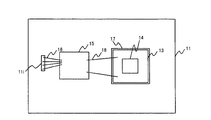
図1は、本発明の第1の実施形態に係る磁気シールドパッケージの斜視図(図1(a))および断面図(図1(b))である。第1の実施形態に係る磁気シールドパッケージ1は、パッケージ基板10、第1の磁気シールド部材11、第2の磁気シールド部材12、圧力検知素子13、磁気デバイス14、集積回路15を有する。図2には、磁気シールドパッケージ1から第2の磁気シールド部材12を外した状態での上面図を示す。
図5は、本発明の第1の実施形態の変形例に係る磁気シールドパッケージの断面図である。図5では、図1と同様の構成要素には同じ記号を付して、その構成要素についての詳細な説明は省略する。本変形例に係る磁気シールドパッケージ2は、第1の実施形態に係る磁気シールドパッケージに第3の磁気シールド部材21を加えた構成である。図6は磁気シールドパッケージ2から第2の磁気シールド部材12を外した状態での斜視図である。
図7は、本発明の第1の実施形態の変形例2に係る磁気シールドパッケージの斜視図(図7(a))および断面図(図7(b))である。図7に示す磁気シールドパッケージ5では、図1の磁気シールドパッケージ1と同じ構成要素は同じ記号を付す。図7に示すように、磁気シールドパッケージ5は、第1の磁気シールド部材11ではなく、第2の磁気シールド部材12に開口部12hを設ける。
図8は、本発明の第2の実施形態に係る磁気シールドパッケージの断面図である。第2の実施形態に係る磁気シールドパッケージ3は、パッケージ基板30、第1の磁気シールド部材31、第2の磁気シールド部材32、圧力検知素子13、磁気デバイス14、集積回路15、半田ボール39を有する。圧力検知素子13、磁気デバイス14、集積回路15等の構成要素は第1の実施形態の磁気シールドパッケージ1と同様であるため、同じ記号を付し、詳細な説明は省略する。
Claims (7)
- 磁気デバイスと、
前記磁気デバイスの下方に設けられた第1の磁性体と、
前記磁気デバイスを覆う第2の磁性体と、
前記磁気デバイスの四方に設けられた第3の磁性体と、を有し、
前記第1の磁性体、または、前記第2の磁性体に開口が設けられ、
前記第2の磁性体は、前記磁気デバイスおよび前記第3の磁性体を覆い、
前記第3の磁性体は、非磁性の接着剤により前記第1の磁性体に接着される、
センサ。 - 磁気デバイスと、
前記磁気デバイスの下に設けられた圧力検知素子と、
前記圧力検知素子の下方に設けられ、前記圧力検知素子の直下の少なくとも一部に第1の開口が設けられた第1の磁性体と、
前記磁気デバイスを覆う第2の磁性体と、
前記磁気デバイスの四方に設けられた第3の磁性体と、を有し、
前記第2の磁性体は、前記磁気デバイスおよび前記第3の磁性体を覆い、
前記第3の磁性体は、非磁性の接着剤により前記第1の磁性体に接着される、
センサ。 - 磁気デバイスと、
前記磁気デバイスの下に設けられた圧力検知素子と、
前記圧力検知素子の下方に設けられ、前記圧力検知素子の直下の少なくとも一部に第1の開口が設けられた第1の磁性体と、
前記磁気デバイスを覆う第2の磁性体と、
前記圧力検知素子の下方に設けられ、前記圧力検知素子の直下の少なくとも一部に第2の開口が設けられた基板と、を有し、
前記第1の磁性体には、複数の前記第1の開口が設けられ、複数の前記第1の開口のそれぞれは、前記第2の開口よりも面積が小さい、
センサ。 - 磁気デバイスと、
前記磁気デバイスの下に設けられた圧力検知素子と、
前記圧力検知素子の下方に設けられ、前記圧力検知素子の直下の少なくとも一部に第1の開口が設けられた第1の磁性体と、
前記磁気デバイスを覆う第2の磁性体と、
前記圧力検知素子の下方に設けられ、前記圧力検知素子の直下の少なくとも一部に第2の開口が設けられた基板と、を有し、
前記第1の開口は、前記第2の開口よりも面積が小さい、
センサ。 - 前記第1の磁性体と前記第2の磁性体とは、磁性粒子を含む接着剤によって接着されている請求項1〜4のいずれか1項に記載のセンサ。
- 前記磁気デバイスの四方に設けられた第3の磁性体を更に有し、
前記第2の磁性体は、前記磁気デバイスおよび前記第3の磁性体を覆い、前記基板は前記第1の磁性体上に設けられ、前記第3の磁性体は非磁性の接着剤により前記基板に接着される請求項3または4に記載のセンサ。 - 前記第2の磁性体は、前記第1の磁性体の上方に設けられる、請求項1〜4のいずれか1項に記載のセンサ。
Priority Applications (3)
| Application Number | Priority Date | Filing Date | Title |
|---|---|---|---|
| JP2014202632A JP6430201B2 (ja) | 2014-09-30 | 2014-09-30 | センサ |
| TW104132266A TW201618271A (zh) | 2014-09-30 | 2015-09-30 | 磁屏蔽封裝體 |
| US14/870,817 US9885762B2 (en) | 2014-09-30 | 2015-09-30 | Magnetic shielded package having magnetic shield members |
Applications Claiming Priority (1)
| Application Number | Priority Date | Filing Date | Title |
|---|---|---|---|
| JP2014202632A JP6430201B2 (ja) | 2014-09-30 | 2014-09-30 | センサ |
Related Child Applications (1)
| Application Number | Title | Priority Date | Filing Date |
|---|---|---|---|
| JP2018202980A Division JP2019012087A (ja) | 2018-10-29 | 2018-10-29 | センサ |
Publications (2)
| Publication Number | Publication Date |
|---|---|
| JP2016070848A JP2016070848A (ja) | 2016-05-09 |
| JP6430201B2 true JP6430201B2 (ja) | 2018-11-28 |
Family
ID=55584131
Family Applications (1)
| Application Number | Title | Priority Date | Filing Date |
|---|---|---|---|
| JP2014202632A Expired - Fee Related JP6430201B2 (ja) | 2014-09-30 | 2014-09-30 | センサ |
Country Status (3)
| Country | Link |
|---|---|
| US (1) | US9885762B2 (ja) |
| JP (1) | JP6430201B2 (ja) |
| TW (1) | TW201618271A (ja) |
Families Citing this family (22)
| Publication number | Priority date | Publication date | Assignee | Title |
|---|---|---|---|---|
| WO2016144039A1 (en) | 2015-03-06 | 2016-09-15 | Samsung Electronics Co., Ltd. | Circuit element package, manufacturing method thereof, and manufacturing apparatus thereof |
| US20170240418A1 (en) * | 2016-02-18 | 2017-08-24 | Knowles Electronics, Llc | Low-cost miniature mems vibration sensor |
| KR102481868B1 (ko) * | 2016-05-04 | 2022-12-28 | 삼성전자주식회사 | 이종의 회로 소자군용 중공 차폐구조 및 그 제조방법 |
| US10477737B2 (en) | 2016-05-04 | 2019-11-12 | Samsung Electronics Co., Ltd. | Manufacturing method of a hollow shielding structure for circuit elements |
| US10477687B2 (en) | 2016-08-04 | 2019-11-12 | Samsung Electronics Co., Ltd. | Manufacturing method for EMI shielding structure |
| KR20180029541A (ko) * | 2016-09-12 | 2018-03-21 | 엘지이노텍 주식회사 | 자성시트 및 이를 포함하는 무선 전력 수신 장치 |
| KR20180032985A (ko) * | 2016-09-23 | 2018-04-02 | 삼성전자주식회사 | 집적회로 패키지 및 그 제조 방법과 집적회로 패키지를 포함하는 웨어러블 디바이스 |
| KR102551657B1 (ko) | 2016-12-12 | 2023-07-06 | 삼성전자주식회사 | 전자파 차폐구조 및 그 제조방법 |
| JP6790956B2 (ja) | 2017-03-27 | 2020-11-25 | Tdk株式会社 | 磁気センサ装置 |
| US10431732B2 (en) * | 2017-05-31 | 2019-10-01 | Globalfoundries Singapore Pte. Ltd. | Shielded magnetoresistive random access memory devices and methods for fabricating the same |
| US10594020B2 (en) | 2017-07-19 | 2020-03-17 | Samsung Electronics Co., Ltd. | Electronic device having antenna element and method for manufacturing the same |
| KR102373931B1 (ko) | 2017-09-08 | 2022-03-14 | 삼성전자주식회사 | 전자파 차폐구조 |
| US10718825B2 (en) * | 2017-09-13 | 2020-07-21 | Nxp B.V. | Stray magnetic field robust magnetic field sensor and system |
| US10893637B2 (en) | 2018-02-21 | 2021-01-12 | Samsung Electronics Co., Ltd. | Electronic device including shield member for shielding at least part of magnetic force generated by magnetic substance and connection portion including property of nonmagnetic substance connected to shield member |
| KR102540241B1 (ko) * | 2018-02-21 | 2023-06-08 | 삼성전자주식회사 | 자성체로부터 발생하는 자기력의 적어도 일부를 차폐하기 위한 차폐 부재 및 차폐 부재와 연결된 비자성체 속성을 갖는 연결부를 포함하는 전자 장치 |
| JP7013346B2 (ja) * | 2018-03-14 | 2022-01-31 | 株式会社東芝 | センサ |
| US10775197B2 (en) | 2018-03-14 | 2020-09-15 | Kabushiki Kaisha Toshiba | Sensor |
| JP6877379B2 (ja) * | 2018-03-14 | 2021-05-26 | 株式会社東芝 | センサ |
| JP2020092114A (ja) * | 2018-12-03 | 2020-06-11 | ソニーセミコンダクタソリューションズ株式会社 | 半導体装置および撮像装置 |
| US11774519B2 (en) * | 2019-08-27 | 2023-10-03 | Texas Instruments Incorporated | Shielded sensor structure and method of making same |
| JP6997892B2 (ja) * | 2021-03-02 | 2022-01-18 | 株式会社東芝 | センサ |
| US11754646B2 (en) | 2021-03-24 | 2023-09-12 | Analog Devices International Unlimited Company | Magnetic sensor system |
Family Cites Families (19)
| Publication number | Priority date | Publication date | Assignee | Title |
|---|---|---|---|---|
| JPS57111427A (en) * | 1980-12-29 | 1982-07-10 | Aisin Seiki Co Ltd | Pressure sensor |
| JPH08204377A (ja) * | 1995-01-24 | 1996-08-09 | Nec Eng Ltd | 遮蔽体 |
| JP2003133778A (ja) * | 2001-10-30 | 2003-05-09 | Hitachi Metals Ltd | 磁気シールド方法 |
| JP3879576B2 (ja) * | 2002-04-16 | 2007-02-14 | ソニー株式会社 | 磁気不揮発性メモリ素子の磁気シールドパッケージ |
| JP2004214451A (ja) * | 2003-01-06 | 2004-07-29 | Hitachi Metals Ltd | 多重構造を有する磁気シールド装置 |
| US7183617B2 (en) * | 2005-02-17 | 2007-02-27 | Taiwan Semiconductor Manufacturing Co., Ltd. | Magnetic shielding for magnetically sensitive semiconductor devices |
| JP4671770B2 (ja) * | 2005-06-10 | 2011-04-20 | 株式会社日立ハイテクノロジーズ | 磁場計測装置 |
| US7436054B2 (en) * | 2006-03-03 | 2008-10-14 | Silicon Matrix, Pte. Ltd. | MEMS microphone with a stacked PCB package and method of producing the same |
| JP4873638B2 (ja) * | 2007-03-05 | 2012-02-08 | 国立大学法人豊橋技術科学大学 | 金属検出器用磁気シールドボックス |
| JP2009036579A (ja) | 2007-07-31 | 2009-02-19 | Alps Electric Co Ltd | 磁気センサパッケージ |
| US20090057885A1 (en) * | 2007-08-30 | 2009-03-05 | Infineon Technologies Ag | Semiconductor device |
| TWI373119B (en) | 2007-12-31 | 2012-09-21 | Ind Tech Res Inst | Semiconductor device with magnetic shielding structure |
| TW201019453A (en) | 2008-11-05 | 2010-05-16 | Windtop Technology Corp | MEMS package |
| US8325951B2 (en) * | 2009-01-20 | 2012-12-04 | General Mems Corporation | Miniature MEMS condenser microphone packages and fabrication method thereof |
| TWI451538B (zh) | 2010-01-19 | 2014-09-01 | 通用微機電系統公司 | 微機電系統(mems)麥克風封裝體及其製造方法 |
| JPWO2011111789A1 (ja) * | 2010-03-10 | 2013-06-27 | 日本電気株式会社 | 磁性体装置及びその製造方法 |
| JP5711705B2 (ja) | 2012-09-10 | 2015-05-07 | 株式会社東芝 | 圧力検知素子及びその製造方法 |
| JP5951454B2 (ja) | 2012-11-20 | 2016-07-13 | 株式会社東芝 | マイクロフォンパッケージ |
| JP6353763B2 (ja) | 2014-09-30 | 2018-07-04 | 新光電気工業株式会社 | 半導体装置及びその製造方法 |
-
2014
- 2014-09-30 JP JP2014202632A patent/JP6430201B2/ja not_active Expired - Fee Related
-
2015
- 2015-09-30 TW TW104132266A patent/TW201618271A/zh unknown
- 2015-09-30 US US14/870,817 patent/US9885762B2/en not_active Expired - Fee Related
Also Published As
| Publication number | Publication date |
|---|---|
| TW201618271A (zh) | 2016-05-16 |
| US9885762B2 (en) | 2018-02-06 |
| US20160091575A1 (en) | 2016-03-31 |
| JP2016070848A (ja) | 2016-05-09 |
Similar Documents
| Publication | Publication Date | Title |
|---|---|---|
| JP6430201B2 (ja) | センサ | |
| US9581571B2 (en) | Acoustic sensor and acoustic sensor system | |
| US9488541B2 (en) | Pressure sensor, microphone, and acoustic processing system | |
| JP2015224903A (ja) | 圧力センサ、マイクロフォン、超音波センサ、血圧センサ及びタッチパネル | |
| JP6275549B2 (ja) | 圧力センサ、マイクロフォン、超音波センサ、血圧センサ及びタッチパネル | |
| CN105988091B (zh) | 半导体装置 | |
| JP2008249406A (ja) | 磁気インピーダンス効果素子及びその製造方法 | |
| JP2018538697A5 (ja) | ||
| JP2021510808A (ja) | センサーパッケージ | |
| JP6235598B2 (ja) | 半導体装置及びその製造方法 | |
| JP2019012087A (ja) | センサ | |
| US20150139467A1 (en) | Acoustic device and microphone package including the same | |
| US20170067787A1 (en) | Pressure sensor, microphone, ultrasonic sensor, blood pressure sensor, and touch panel | |
| JP2007263951A (ja) | 磁気センサ | |
| CN207061864U (zh) | 一种芯片的安装结构 | |
| JP2015200546A (ja) | センサ構造 | |
| JP5139822B2 (ja) | 磁界プローブ | |
| JP2012088191A (ja) | 電流センサ | |
| JP6517954B2 (ja) | 圧力センサ、マイクロフォン、超音波センサ、血圧センサ及びタッチパネル | |
| US10775197B2 (en) | Sensor | |
| US10546819B2 (en) | Semiconductor device and method of manufacturing the same | |
| JP2014202737A (ja) | 電流センサ | |
| JP2014006118A (ja) | 電流センサ | |
| JP6877379B2 (ja) | センサ | |
| JP2008311379A (ja) | 半導体装置 |
Legal Events
| Date | Code | Title | Description |
|---|---|---|---|
| A621 | Written request for application examination |
Free format text: JAPANESE INTERMEDIATE CODE: A621 Effective date: 20160916 |
|
| RD02 | Notification of acceptance of power of attorney |
Free format text: JAPANESE INTERMEDIATE CODE: A7422 Effective date: 20160916 |
|
| A521 | Request for written amendment filed |
Free format text: JAPANESE INTERMEDIATE CODE: A821 Effective date: 20160916 |
|
| A977 | Report on retrieval |
Free format text: JAPANESE INTERMEDIATE CODE: A971007 Effective date: 20170630 |
|
| A131 | Notification of reasons for refusal |
Free format text: JAPANESE INTERMEDIATE CODE: A131 Effective date: 20170725 |
|
| A521 | Request for written amendment filed |
Free format text: JAPANESE INTERMEDIATE CODE: A523 Effective date: 20170907 |
|
| A131 | Notification of reasons for refusal |
Free format text: JAPANESE INTERMEDIATE CODE: A131 Effective date: 20180220 |
|
| A521 | Request for written amendment filed |
Free format text: JAPANESE INTERMEDIATE CODE: A523 Effective date: 20180413 |
|
| TRDD | Decision of grant or rejection written | ||
| A01 | Written decision to grant a patent or to grant a registration (utility model) |
Free format text: JAPANESE INTERMEDIATE CODE: A01 Effective date: 20181002 |
|
| A61 | First payment of annual fees (during grant procedure) |
Free format text: JAPANESE INTERMEDIATE CODE: A61 Effective date: 20181031 |
|
| R151 | Written notification of patent or utility model registration |
Ref document number: 6430201 Country of ref document: JP Free format text: JAPANESE INTERMEDIATE CODE: R151 |
|
| LAPS | Cancellation because of no payment of annual fees |