JP6430201B2 - Sensor - Google Patents
Sensor Download PDFInfo
- Publication number
- JP6430201B2 JP6430201B2 JP2014202632A JP2014202632A JP6430201B2 JP 6430201 B2 JP6430201 B2 JP 6430201B2 JP 2014202632 A JP2014202632 A JP 2014202632A JP 2014202632 A JP2014202632 A JP 2014202632A JP 6430201 B2 JP6430201 B2 JP 6430201B2
- Authority
- JP
- Japan
- Prior art keywords
- magnetic
- magnetic shield
- opening
- shield member
- magnetic body
- Prior art date
- Legal status (The legal status is an assumption and is not a legal conclusion. Google has not performed a legal analysis and makes no representation as to the accuracy of the status listed.)
- Expired - Fee Related
Links
- 230000005291 magnetic effect Effects 0.000 claims description 259
- 239000000853 adhesive Substances 0.000 claims description 48
- 230000001070 adhesive effect Effects 0.000 claims description 45
- 239000000758 substrate Substances 0.000 claims description 33
- 238000001514 detection method Methods 0.000 claims description 25
- 239000006249 magnetic particle Substances 0.000 claims description 12
- 230000004048 modification Effects 0.000 description 18
- 238000012986 modification Methods 0.000 description 18
- 230000000694 effects Effects 0.000 description 17
- XEEYBQQBJWHFJM-UHFFFAOYSA-N Iron Chemical compound [Fe] XEEYBQQBJWHFJM-UHFFFAOYSA-N 0.000 description 8
- 230000035699 permeability Effects 0.000 description 8
- 229910000679 solder Inorganic materials 0.000 description 8
- 239000012212 insulator Substances 0.000 description 4
- 229910052742 iron Inorganic materials 0.000 description 4
- 229920001296 polysiloxane Polymers 0.000 description 4
- BQCADISMDOOEFD-UHFFFAOYSA-N Silver Chemical compound [Ag] BQCADISMDOOEFD-UHFFFAOYSA-N 0.000 description 3
- 239000004020 conductor Substances 0.000 description 3
- 239000000463 material Substances 0.000 description 3
- 229910000889 permalloy Inorganic materials 0.000 description 3
- 230000000644 propagated effect Effects 0.000 description 3
- 230000035945 sensitivity Effects 0.000 description 3
- 229910052709 silver Inorganic materials 0.000 description 3
- 239000004332 silver Substances 0.000 description 3
- UQSXHKLRYXJYBZ-UHFFFAOYSA-N Iron oxide Chemical compound [Fe]=O UQSXHKLRYXJYBZ-UHFFFAOYSA-N 0.000 description 2
- PXHVJJICTQNCMI-UHFFFAOYSA-N Nickel Chemical compound [Ni] PXHVJJICTQNCMI-UHFFFAOYSA-N 0.000 description 2
- 229910003460 diamond Inorganic materials 0.000 description 2
- 239000010432 diamond Substances 0.000 description 2
- 238000005530 etching Methods 0.000 description 2
- 239000011859 microparticle Substances 0.000 description 2
- 239000002105 nanoparticle Substances 0.000 description 2
- 239000002245 particle Substances 0.000 description 2
- 238000004080 punching Methods 0.000 description 2
- 238000004381 surface treatment Methods 0.000 description 2
- 229910000975 Carbon steel Inorganic materials 0.000 description 1
- 229910000976 Electrical steel Inorganic materials 0.000 description 1
- 239000004593 Epoxy Substances 0.000 description 1
- 239000004642 Polyimide Substances 0.000 description 1
- 230000002378 acidificating effect Effects 0.000 description 1
- 239000011230 binding agent Substances 0.000 description 1
- 239000010962 carbon steel Substances 0.000 description 1
- 238000005260 corrosion Methods 0.000 description 1
- 230000007797 corrosion Effects 0.000 description 1
- 239000003822 epoxy resin Substances 0.000 description 1
- 239000011521 glass Substances 0.000 description 1
- -1 iron Chemical compound 0.000 description 1
- OBACEDMBGYVZMP-UHFFFAOYSA-N iron platinum Chemical compound [Fe].[Fe].[Pt] OBACEDMBGYVZMP-UHFFFAOYSA-N 0.000 description 1
- 239000000696 magnetic material Substances 0.000 description 1
- 238000000034 method Methods 0.000 description 1
- 239000000203 mixture Substances 0.000 description 1
- 229910052759 nickel Inorganic materials 0.000 description 1
- 229920000647 polyepoxide Polymers 0.000 description 1
- 229920001721 polyimide Polymers 0.000 description 1
- 229910000702 sendust Inorganic materials 0.000 description 1
- 229910000859 α-Fe Inorganic materials 0.000 description 1
Images


Classifications
-
- G—PHYSICS
- G01—MEASURING; TESTING
- G01R—MEASURING ELECTRIC VARIABLES; MEASURING MAGNETIC VARIABLES
- G01R33/00—Arrangements or instruments for measuring magnetic variables
- G01R33/0017—Means for compensating offset magnetic fields or the magnetic flux to be measured; Means for generating calibration magnetic fields
-
- G—PHYSICS
- G01—MEASURING; TESTING
- G01R—MEASURING ELECTRIC VARIABLES; MEASURING MAGNETIC VARIABLES
- G01R33/00—Arrangements or instruments for measuring magnetic variables
- G01R33/0047—Housings or packaging of magnetic sensors ; Holders
-
- G—PHYSICS
- G01—MEASURING; TESTING
- G01R—MEASURING ELECTRIC VARIABLES; MEASURING MAGNETIC VARIABLES
- G01R33/00—Arrangements or instruments for measuring magnetic variables
- G01R33/007—Environmental aspects, e.g. temperature variations, radiation, stray fields
- G01R33/0076—Protection, e.g. with housings against stray fields
-
- G—PHYSICS
- G01—MEASURING; TESTING
- G01R—MEASURING ELECTRIC VARIABLES; MEASURING MAGNETIC VARIABLES
- G01R33/00—Arrangements or instruments for measuring magnetic variables
- G01R33/02—Measuring direction or magnitude of magnetic fields or magnetic flux
- G01R33/025—Compensating stray fields
-
- G—PHYSICS
- G01—MEASURING; TESTING
- G01R—MEASURING ELECTRIC VARIABLES; MEASURING MAGNETIC VARIABLES
- G01R33/00—Arrangements or instruments for measuring magnetic variables
- G01R33/02—Measuring direction or magnitude of magnetic fields or magnetic flux
- G01R33/06—Measuring direction or magnitude of magnetic fields or magnetic flux using galvano-magnetic devices
- G01R33/09—Magnetoresistive devices
- G01R33/093—Magnetoresistive devices using multilayer structures, e.g. giant magnetoresistance sensors
-
- H—ELECTRICITY
- H01—ELECTRIC ELEMENTS
- H01L—SEMICONDUCTOR DEVICES NOT COVERED BY CLASS H10
- H01L2224/00—Indexing scheme for arrangements for connecting or disconnecting semiconductor or solid-state bodies and methods related thereto as covered by H01L24/00
- H01L2224/01—Means for bonding being attached to, or being formed on, the surface to be connected, e.g. chip-to-package, die-attach, "first-level" interconnects; Manufacturing methods related thereto
- H01L2224/42—Wire connectors; Manufacturing methods related thereto
- H01L2224/47—Structure, shape, material or disposition of the wire connectors after the connecting process
- H01L2224/48—Structure, shape, material or disposition of the wire connectors after the connecting process of an individual wire connector
- H01L2224/481—Disposition
- H01L2224/48135—Connecting between different semiconductor or solid-state bodies, i.e. chip-to-chip
- H01L2224/48137—Connecting between different semiconductor or solid-state bodies, i.e. chip-to-chip the bodies being arranged next to each other, e.g. on a common substrate
-
- H—ELECTRICITY
- H01—ELECTRIC ELEMENTS
- H01L—SEMICONDUCTOR DEVICES NOT COVERED BY CLASS H10
- H01L2224/00—Indexing scheme for arrangements for connecting or disconnecting semiconductor or solid-state bodies and methods related thereto as covered by H01L24/00
- H01L2224/01—Means for bonding being attached to, or being formed on, the surface to be connected, e.g. chip-to-package, die-attach, "first-level" interconnects; Manufacturing methods related thereto
- H01L2224/42—Wire connectors; Manufacturing methods related thereto
- H01L2224/47—Structure, shape, material or disposition of the wire connectors after the connecting process
- H01L2224/49—Structure, shape, material or disposition of the wire connectors after the connecting process of a plurality of wire connectors
- H01L2224/491—Disposition
- H01L2224/49105—Connecting at different heights
- H01L2224/49109—Connecting at different heights outside the semiconductor or solid-state body
-
- H—ELECTRICITY
- H01—ELECTRIC ELEMENTS
- H01L—SEMICONDUCTOR DEVICES NOT COVERED BY CLASS H10
- H01L2924/00—Indexing scheme for arrangements or methods for connecting or disconnecting semiconductor or solid-state bodies as covered by H01L24/00
- H01L2924/15—Details of package parts other than the semiconductor or other solid state devices to be connected
- H01L2924/161—Cap
- H01L2924/1615—Shape
- H01L2924/16152—Cap comprising a cavity for hosting the device, e.g. U-shaped cap
Landscapes
- Physics & Mathematics (AREA)
- Condensed Matter Physics & Semiconductors (AREA)
- General Physics & Mathematics (AREA)
- Health & Medical Sciences (AREA)
- Engineering & Computer Science (AREA)
- Environmental & Geological Engineering (AREA)
- Toxicology (AREA)
- Shielding Devices Or Components To Electric Or Magnetic Fields (AREA)
- Measuring Magnetic Variables (AREA)
- Mram Or Spin Memory Techniques (AREA)
- Hall/Mr Elements (AREA)
- Measuring Fluid Pressure (AREA)
Description
本発明の実施形態は磁気シールドパッケージに関する。 Embodiments described herein relate generally to a magnetic shield package.
磁気デバイスを用いたセンサは、外部からの磁気ノイズの影響を受ける。そこで、磁気デバイスを磁気シールド部材で囲うことにより、外部からの磁気的影響を低減させる磁気シールドパッケージが提案されている。 Sensors using magnetic devices are affected by external magnetic noise. Therefore, a magnetic shield package has been proposed in which the magnetic effect is reduced by enclosing the magnetic device with a magnetic shield member.
磁気シールドパッケージ内に音波を検出する圧力検知素子を搭載する場合、磁気シールドパッケージの適切な位置に開口が設けられていないと、パッケージ内に音波を効率よく伝搬させることができず、圧力検知の感度を高めることができない。 When a pressure detection element that detects sound waves is installed in the magnetic shield package, if the opening is not provided at an appropriate position in the magnetic shield package, sound waves cannot be efficiently propagated in the package, and pressure detection is not possible. Sensitivity cannot be increased.
そこで本発明は、外部からの磁気ノイズの影響を低減しながらも、センサ感度を高めることができる磁気シールドパッケージを提供することを目的とする。 Accordingly, an object of the present invention is to provide a magnetic shield package that can increase the sensitivity of a sensor while reducing the influence of external magnetic noise.
上記目的を達成するために、本発明の実施形態による磁気シールドパッケージは、磁気デバイスと、前記磁気デバイスの下方に設けられた第1の磁気シールド部材と、前記第1の磁気シールド部材上に設けられ、前記磁気デバイスを覆う第2のシールド部材とを有し、前記第1の磁気シールド部材の外周に接しない位置、または前記第2の磁気シールド部材の上面、のいずれかに開口が設けられる。 In order to achieve the above object, a magnetic shield package according to an embodiment of the present invention is provided with a magnetic device, a first magnetic shield member provided below the magnetic device, and the first magnetic shield member. A second shield member that covers the magnetic device, and an opening is provided either at a position that does not contact the outer periphery of the first magnetic shield member or at the upper surface of the second magnetic shield member. .
以下、本発明の実施形態について図面を参照して説明する。 Embodiments of the present invention will be described below with reference to the drawings.
(第1の実施形態)
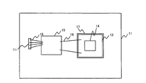
図1は、本発明の第1の実施形態に係る磁気シールドパッケージの斜視図(図1(a))および断面図(図1(b))である。第1の実施形態に係る磁気シールドパッケージ1は、パッケージ基板10、第1の磁気シールド部材11、第2の磁気シールド部材12、圧力検知素子13、磁気デバイス14、集積回路15を有する。図2には、磁気シールドパッケージ1から第2の磁気シールド部材12を外した状態での上面図を示す。
(First embodiment)
1A and 1B are a perspective view (FIG. 1A) and a cross-sectional view (FIG. 1B) of a magnetic shield package according to a first embodiment of the present invention. The
磁気シールドパッケージ1は、音波等を電気的信号に変換するために用いられる。磁気デバイス14は、GMR(Giant Magneto Resistance)素子のように、外部磁界や外部からの圧力によって抵抗などの電気的性能が変化する素子である。磁気デバイス14は、圧力検知素子13上に配置される。
The
圧力検知素子13は、Siを加工したMEMS(Micro Electro Mechanical System)素子等によって構成される。圧力検知素子13は、外部からの音波等を受けて振動する。圧力検知素子13が振動すると、磁気デバイス14に応力が加わり、磁気デバイスの抵抗等の電気的性能が変化する。このようにして、音波等を電気的信号に変換することができる。
The
磁気デバイス14は、外部からの不要磁気ノイズの影響を受けて電気的性能が変化してしまう。そこで、第1の磁気シールド部材11および第2の磁気シールド部材12で磁気デバイス14の周囲を囲うことによって、磁気シールドパッケージ1内を磁気的に遮蔽する。これによって、磁気デバイス14に対する外部からの不要磁界ノイズの影響を低減することができる。ただし、第1の磁気シールド部材11および第2の磁気シールド部材12によって完全に圧力検知素子13および磁気デバイス14を覆うと、パッケージ内に効率良く音波を伝搬させることができない。そこで、第1の磁気シールド部材11に開口部11hを設ける。開口部11hについては後程詳細に説明する。
The electrical performance of the
磁気シールドパッケージ1の構成について説明する。パッケージ基板10は、FR4等のガラスエポキシ基板等である。パッケージ基板10は、1層または複数層の配線層を含む。パッケージ基板10は、LGA(Land Grid Array)タイプでも良いし、BGA(Ball Grid Array)タイプでも良い。図1に示す例は、LGAタイプのパッケージ基板10であって、第1の配線層10aおよび第2の配線層10bが設けられる。第2の配線層10bは電極として用いられる。第1の配線層10aと第2の配線層10bとはビア10cによって接続される。
The configuration of the
パッケージ基板10上には、第1の磁気シールド部材11および第2の磁気シールド部材12が設けられる。パッケージ基板10上に板状の第1の磁気シールド部材11が接着される。第1の磁気シールド部材11上には、磁気デバイス14の上部と側面を覆う磁気シールド部材12が設けられる。こうして、第1の磁気シールド部材11および第2の磁気シールド部材が、磁気デバイス14の周囲を囲う。なお、図1では、第1の磁気シールド部材11が板状であり、第2の磁気シールド部材12が直方体から一面が除かれたような形状であるとして示しているが、第1の磁気シールド部材11と第2の磁気シールド部材12の形状はこれに限られない。第1の磁気シールド部材11および第2の磁気シールド部材12によって磁気デバイス14の周囲を囲うことができれば良い。
A first
第1の磁気シールド部材11および第2の磁気シールド部材12の材質は鉄、炭素鋼、珪素鋼、パーマロイ等の軟磁性体が考えられる。第1の磁気シールド部材11と第2の磁気シールド部材12の材質は同じでも良いし、異なっても良い。
The material of the first
磁気シールドパッケージ1の磁界シールド効果は、第1および第2の磁気シールド部材11,12の比透磁率μrと厚さtmにより決まる。磁気シールド部材の厚さtmをミリメートル単位で表した場合、比透磁率μrと厚さtmの積を10以上にすると、10dB以上の磁界シールド効果を得ることができる。
The magnetic field shielding effect of the
第1の磁気シールド部材11および第2の磁気シールド部材12は、例えば、第1の接着剤16によって接着される。第1の接着剤16は、比透磁率が2以上の磁性粒子等を用いると、第1の磁気シールド部材11と第2の磁気シールド部材12の磁路が繋がり、磁界シールド効果を高めることができる。
The first
図3は第1の接着剤16の厚さと磁界シールド効果との関係を表すグラフである。第1の接着剤16として、非磁性の接着剤を用いた場合と、比透磁率20の磁性粒子を含む接着剤を用いた場合とを比較した。非磁性の接着剤を用いた場合、第1の接着剤16の厚さ3μm以上で磁界シールド効果が48dB以下となり、厚さ30μmの場合には、磁界シールド効果が34dBとなった。一方、非磁性粒子を含む接着剤を用いた場合、第1の接着剤16の厚さが30μm以下の範囲で48dB以上の高い磁界シールド効果が得られた。この比較結果からも、第1の接着剤16として磁性粒子が含まれる接着剤を用いると、非磁性の接着剤を用いた場合よりも高い磁気シールド効果が得られることが分かる。
FIG. 3 is a graph showing the relationship between the thickness of the
第1の接着剤16に用いられる磁性粒子は、直径1μm〜数10μmのマイクロ粒子、直径数nm〜数10nmのナノ粒子、もしくはその両方が混合されたものが考えられる。例えば、鉄、パーマロイ、フェライト、センダスト等の鉄やニッケルを主成分にするマイクロ粒子や、鉄や酸化鉄、鉄白金等のナノ粒子が考えられる。また、粒子のバインダーはエポキシ樹脂やシリコーン等が考えられ、第1の磁気シールド部材と第2の磁気シールド部材の接合性の良さから選択すればよい。なお、第1の接着剤16として、シリコーン等の非酸性の接着剤や絶縁体や銀ペースト、はんだ等の導体の接着剤を用いることもできる。
The magnetic particles used for the first adhesive 16 may be a mixture of microparticles having a diameter of 1 μm to several tens of μm, nanoparticles having a diameter of several nm to several tens of nm, or both. For example, microparticles mainly composed of iron and nickel such as iron, permalloy, ferrite, and sendust, and nanoparticles such as iron, iron oxide, and iron platinum are conceivable. The binder of the particles may be an epoxy resin, silicone, or the like, and may be selected from the good bondability between the first magnetic shield member and the second magnetic shield member. As the
また、第1の磁気シールド部材と第2の磁気シールド部材は、比透磁率が2以上の磁性粒子等を用いた接着剤で接着される以外にも、例えば両面テープで接着することも考えられる。 Further, the first magnetic shield member and the second magnetic shield member may be bonded with, for example, a double-sided tape, in addition to being bonded with an adhesive using magnetic particles having a relative magnetic permeability of 2 or more. .
圧力検知素子13は第1の磁気シールド部材11上に設けられる。圧力検知素子13と磁気シールド部材11とは、第2の接着剤17によって接着される。第2の接着剤17として、磁性粒子を含まないシリコーンなどの非磁性の接着剤や絶縁体や銀ペースト、はんだ等の非磁性の導体接着剤等が用いられる。
The
圧力検知素子13上には、単数または複数個の磁気デバイス14が設けられる。磁気デバイス14を複数設けることで、音波に対する感度を向上させることができる。磁気デバイス14は、圧力検知素子13上に設けられた配線やワイヤ18を介して集積回路15に電気的に接続される。圧力検知素子13および磁気デバイス14を用いて検知されたアナログ信号は、集積回路15に入力される。
On the
集積回路15は、入力されたアナログ信号を信号処理し、ディジタル信号を出力する。集積回路15から出力されたディジタル信号は、ワイヤ18やパッケージ基板上を通り、電極10bに出力される。ワイヤ18をパッケージ基板に接続する必要があるため、図2に示すように第1の磁気シールド部材11にはワイヤ18を通すための開口11iが設けられている。なお、本実施形態の集積回路15は、第1の磁気シールド部材11および第2の磁気シールド部材12に囲まれた空間内に配置されているが、第1の磁気シールド部材11および第2の磁気シールド部材12で囲まれた空間の外に配置することもできる。
The
次に、第1の磁気シールド部材11に設けられる開口部11hについて説明する。開口部11hは、圧力検知素子13の下方に設けられる。圧力検知素子13の下方に開口部11hを設けることによって、磁気シールドパッケージ1内に音波を効率よく伝搬させることができる。また、第1の磁気シールド部材11の開口部11hの下方には、パッケージ基板10の開口部10hが設けられる。
Next, the
図4に、第1の磁気シールド部材11の開口部11hおよびパッケージ基板10の開口部10hの上面透視図を示す。図4では、第1の磁気シールド部材11の開口部11hを実線で示し、パッケージ基板10の開口部10hを破線で示す。パッケージ基板10には例えば円形の開口から成る開口部10hが設けられる。第1の磁気シールド部材11の開口部11hは、図4(a)に示すように円形(例えばパッケージ基板10と同心円)の開口部でも良いし、図4(b)に示すように扇状の開口から成る開口部でも良いし、図4(c)に示すようにパッケージ基板10の開口よりも面積が小さい円形の複数の開口から成る開口部でも良いし、図4(d)に示すようにパッケージ基板10の開口よりも面積が十分小さい複数の開口から成る網目状の開口部であっても良い。図4(a)の磁気シールド部材の開口部11hおよびパッケージ基板10の開口部10hの寸法は、ヘルムホルツ共鳴がおこらないように、パッケージ基板厚さ、ダイヤフラムの空間等を考慮し、設計する。また図4(d)の第1の磁気シールド部材11の開口部11hの各開口の寸法は、センシングする最大周波数における音波の波長の1/1000以上にするとよい。具体的には最大周波数を10kHzとすると、波長は3.4cmになるので、開口の直径、または最も短い辺の寸法は1/1000以上だと34μm以上にするとよい。また、開口の形状は、上記に限定されることはなく、楕円、多角形、正方形、長方形、菱形、三角形、星型などでも良い。
FIG. 4 is a top perspective view of the
なお、開口部10hが開口部11hよりも大きくても良いし、開口部11hが開口部10hよりも大きくても良い。図4(a)や図4(c)のような円形の開口はドリルによって開けられても良いし、打ち抜きやエッチングによって加工されても良い。また、図4(b)や図4(d)のような開口は打ち抜きやエッチングによって加工されても良い。
The
磁気シールド効果を図4(a)〜(d)間で比較すると、図4(a)場合には39.8dBとなり、図4(b)の場合には49.4dBとなり、図4(c)の場合には49.5dBとなり、図4(d)の場合には、49.8dBとなった。つまり、パッケージ基板10の開口部10hと同じ円形の開口部11hよりも、パッケージ基板10の開口部10hよりも小さい複数の開口から成る開口部11hの方が高い磁界シールド効果を得ることができる。
4A to 4D, the magnetic shielding effect is 39.8 dB in the case of FIG. 4A, 49.4 dB in the case of FIG. 4B, and FIG. In this case, it was 49.5 dB, and in the case of FIG. 4D, it was 49.8 dB. In other words, the
このような磁気シールドパッケージ1は、例えばGMR素子等の磁気デバイスを用いた音響センサや、磁界強度を測定する電流センサ、MRAM(Magnetoresistive random access memory)の磁気シールドパッケージに用いることができる。
Such a
(第1の実施形態の変形例)
図5は、本発明の第1の実施形態の変形例に係る磁気シールドパッケージの断面図である。図5では、図1と同様の構成要素には同じ記号を付して、その構成要素についての詳細な説明は省略する。本変形例に係る磁気シールドパッケージ2は、第1の実施形態に係る磁気シールドパッケージに第3の磁気シールド部材21を加えた構成である。図6は磁気シールドパッケージ2から第2の磁気シールド部材12を外した状態での斜視図である。
(Modification of the first embodiment)
FIG. 5 is a cross-sectional view of a magnetic shield package according to a modification of the first embodiment of the present invention. In FIG. 5, the same components as those in FIG. The magnetic shield package 2 according to this modification has a configuration in which a third
第3の磁気シールド部材21は、第1の磁気シールド部材11上に配置され、圧力検知素子13と磁気デバイス14の四方を囲う。圧力検知素子13と磁気デバイス14の上方は、圧力検知素子13と集積回路15とを接続するワイヤ18を通すために第3の磁気シールド部材21が設けられない。もしくは、圧力検知素子13と磁気デバイス14の上方には、ワイヤボンディングの妨げにならない部分に第3の磁気シールド部材21を設けても良い。
The third
第3の磁気シールド部材21は、第3の接着剤22を用いて第1の磁気シールド部材11に接着される。第3の接着剤22としては、磁性粒子を含まないシリコーン等の非磁性の接着剤や、絶縁体や、銀ペーストや、はんだ等の非磁性の導体の接着剤が用いられる。このように第3の磁気シールド部材21を設けることで、磁気デバイス14周辺の磁気シールド効果をさらに高めることができる。
The third
第3の磁気シールド部材21の有無および、第3の接着剤22として非磁性の接着剤を用いる点について、磁界解析結果を用いて説明する。(1)第3の磁気シールド部材21を配置しない場合(第1の磁気シールドパッケージ1)と、(2)第2の磁気シールドパッケージ2において50μm厚の非磁性の第3の接着剤22によって第3の磁気シールド部材を接着した場合と、(3)第2の磁気シールドパッケージ2において10μm厚の磁性粒子を含む接着剤で接着した場合の磁界シールド効果について比較した。
The presence / absence of the third
このとき、第1の磁気シールド部材11、第2の磁気シールド部材13、第3の磁気シールド部材21は比透磁率5000のパーマロイで、第1の磁気シールド部材11および第2の磁気シールド部材13の厚さは0.2mmとした。第1の接着剤16には厚さ10μmで比透磁率20の磁性粒子を含む接着剤を用いた。第1の磁気シールド部材11の開口部11hは、図4(c)に示すような形状とした。第3の磁気シールド部材21は高さが0.5mmで、外周が1辺の1.2mmの正方形、内周が0.8mmの正方形とした。
At this time, the first
その結果、(1)第3の磁気シールド部材21を配置しない場合には、磁界シールド効果は49.5dBとなった。(2)第2の磁気シールドパッケージ2において50μm厚の非磁性の第3の接着剤22によって第3の磁気シールド部材を接着した場合には、56.5dBとなった。(3)第2の磁気シールドパッケージ2において10μm厚の磁性粒子を含む接着剤で接着した場合には、51.5dBとなった。つまり、第3の磁気シールド部材を配置することにより、磁界シールド効果は上昇し、特に第3の接着剤22として、非磁性体の接着剤を用いた方が磁性体の接着剤を用いた場合よりも磁界シールド効果が高くなることが示された。
As a result, (1) when the third
(第1の実施形態の変形例2)
図7は、本発明の第1の実施形態の変形例2に係る磁気シールドパッケージの斜視図(図7(a))および断面図(図7(b))である。図7に示す磁気シールドパッケージ5では、図1の磁気シールドパッケージ1と同じ構成要素は同じ記号を付す。図7に示すように、磁気シールドパッケージ5は、第1の磁気シールド部材11ではなく、第2の磁気シールド部材12に開口部12hを設ける。
(Modification 2 of the first embodiment)
FIG. 7 is a perspective view (FIG. 7A) and a cross-sectional view (FIG. 7B) of a magnetic shield package according to Modification 2 of the first embodiment of the present invention. In the
図7では、開口部12hが集積回路15の直上に設けられた場合の磁気シールドパッケージ5を示している。しかし、開口部12hは集積回路15の直上に限定されず、第2の磁気シールド部材12のどこに設けても良い。ただし、第2の磁気シールド部材12の第1の磁気シールド部材11と接しない面であって、外周に接しない箇所に設けると開口部の加工が容易である。開口部12hは、円、楕円、多角形、正方形、長方形、菱形、三角形、星型など、どのような形状でも良い。また、図4を用いて説明した開口部11hと同様に、開口部12hは、1つの開口から構成されても良いし、複数の開口から構成されても良い。
FIG. 7 shows the
さらに、第1の実施形態の変形例2は変形例1と組み合わせても良い。つまり、磁気シールドパッケージ5の圧力検知素子13と磁気デバイス14の四方を囲う第3の磁気シールド部材21を設けても良い。
Furthermore, the second modification of the first embodiment may be combined with the first modification. That is, a third
(第2の実施形態)
図8は、本発明の第2の実施形態に係る磁気シールドパッケージの断面図である。第2の実施形態に係る磁気シールドパッケージ3は、パッケージ基板30、第1の磁気シールド部材31、第2の磁気シールド部材32、圧力検知素子13、磁気デバイス14、集積回路15、半田ボール39を有する。圧力検知素子13、磁気デバイス14、集積回路15等の構成要素は第1の実施形態の磁気シールドパッケージ1と同様であるため、同じ記号を付し、詳細な説明は省略する。
(Second Embodiment)
FIG. 8 is a cross-sectional view of a magnetic shield package according to the second embodiment of the present invention. The
磁気シールドパッケージ3では、第1の磁気シールド部材31がパッケージ基板10の下に設けられる。そして、第2の磁気シールド部材32は、パッケージ基板10の四方を囲んで、第1の磁気シールド部材31に第1の接着剤16を用いて接着される。これによって、第1の磁気シールド部材31と第2の磁気シールド部材32とによって、磁気デバイス14の周囲を囲うことができ、外部からの不要磁気ノイズの影響を低減することができる。更に、第1の接着剤16は、第1の実施形態にて説明したとおり、磁性粒子を含む比透磁率2以上の接着剤を用いると、磁界シールド効果を高めることができる。
In the
パッケージ基板30は、磁気シールドパッケージ3の外部へ電極を取り出すために、半田ボール39が搭載されている。このため、第1の磁気シールド部材31の半田ボール39直下の部分にも開口部31jが設けられる。例えば、半田ボール39の直径を0.3mm、開口部31jの直径を0.6mmとする。
The
なお、磁気シールドパッケージ3は、回路配線との短絡を防ぐ目的や、腐食に耐性持たせる目的で、絶縁体の表面処理を施しても良い。表面処理の材質にはポリイミド等が用いられる。
The
また、本実施形態においても、第1の実施形態の変形例と同様の変形が可能である。図9に示すように、変形例1に係る磁気シールドパッケージ4は、第3の磁気シールド部材21を更に有し、第3の磁気シールド部材21が、パッケージ基板30上に配置され、圧力検知素子13と磁気デバイス14の四方を囲うように配置する。第3の磁気シールド部材21とパッケージ基板30は第3の接着剤を用いて接着される。
Also in this embodiment, the same modification as the modification of the first embodiment is possible. As shown in FIG. 9, the
また、図10に示すように、変形例2に係る磁気シールドパッケージ6は、第2の磁気シールド部材32に開口部32hを設ける。開口部32hを設ける位置は第2の磁気シールド部材32のどこでも良く、開口部32hは1つの開口から構成されても複数の開口から構成されても良く、開口はどのような形状でも良い。さらに、変形例1と変形例2とは組み合わせても良い。
Further, as shown in FIG. 10, the magnetic shield package 6 according to the modified example 2 is provided with an
以上本発明のいくつかの実施形態を説明したが、これらの実施形態は、例として提示したものであり、発明の範囲を限定することは意図していない。これら新規な実施形態は、その他の様々な形態で実施されることが可能であり、発明の要旨を逸脱しない範囲で、種々の省略、置き換え、変更を行うことができる。これら実施形態やその変形は、発明の範囲や要旨に含まれるとともに、特許請求の範囲に記載された発明とその均等の範囲に含まれる。 Although several embodiments of the present invention have been described above, these embodiments are presented as examples and are not intended to limit the scope of the invention. These novel embodiments can be implemented in various other forms, and various omissions, replacements, and changes can be made without departing from the scope of the invention. These embodiments and modifications thereof are included in the scope and gist of the invention, and are included in the invention described in the claims and the equivalents thereof.
1,2,3,4,5,6…磁気シールドパッケージ、 10,30…パッケージ基板、 10a,30a…第1の配線層、 10b,30b…第2の配線層、 10c,30c…ビア、 10h,12h,30h,32h…開口部、 11,31…第1の磁気シールド部材、 11h,31h…開口部、 11i…開口部、 12,32…第2の磁気シールド部材、 13…圧力検知素子、 14…磁気デバイス、 15…集積回路、 16…第1の接着剤、 17…第2の接着剤、 18…ワイヤ、 31j…開口部、 39…半田ボール
1, 2, 3, 4, 5, 6 ... Magnetic shield package, 10, 30 ... Package substrate, 10a, 30a ... First wiring layer, 10b, 30b ... Second wiring layer, 10c, 30c ... Via, 10h , 12h, 30h, 32h ... opening, 11, 31 ... first magnetic shield member, 11h, 31h ... opening, 11i ... opening, 12, 32 ... second magnetic shield member, 13 ... pressure sensing element, DESCRIPTION OF
Claims (7)
前記磁気デバイスの下方に設けられた第1の磁性体と、
前記磁気デバイスを覆う第2の磁性体と、
前記磁気デバイスの四方に設けられた第3の磁性体と、を有し、
前記第1の磁性体、または、前記第2の磁性体に開口が設けられ、
前記第2の磁性体は、前記磁気デバイスおよび前記第3の磁性体を覆い、
前記第3の磁性体は、非磁性の接着剤により前記第1の磁性体に接着される、
センサ。 A magnetic device;
A first magnetic body provided below the magnetic device;
A second magnetic body covering the magnetic device;
A third magnetic body provided on all sides of the magnetic device,
An opening is provided in the first magnetic body or the second magnetic body ,
The second magnetic body is not covered with the magnetic device and the third magnetic body,
The third magnetic body is bonded to the first magnetic body by a nonmagnetic adhesive.
Sensor .
前記磁気デバイスの下に設けられた圧力検知素子と、
前記圧力検知素子の下方に設けられ、前記圧力検知素子の直下の少なくとも一部に第1の開口が設けられた第1の磁性体と、
前記磁気デバイスを覆う第2の磁性体と、
前記磁気デバイスの四方に設けられた第3の磁性体と、を有し、
前記第2の磁性体は、前記磁気デバイスおよび前記第3の磁性体を覆い、
前記第3の磁性体は、非磁性の接着剤により前記第1の磁性体に接着される、
センサ。 A magnetic device;
A pressure sensing element provided under the magnetic device;
A first magnetic body provided below the pressure detection element, and having a first opening provided at least in part immediately below the pressure detection element;
A second magnetic body covering the magnetic device;
A third magnetic body provided on all sides of the magnetic device,
The second magnetic body is not covered with the magnetic device and the third magnetic body,
The third magnetic body is bonded to the first magnetic body by a nonmagnetic adhesive.
Sensor .
前記磁気デバイスの下に設けられた圧力検知素子と、
前記圧力検知素子の下方に設けられ、前記圧力検知素子の直下の少なくとも一部に第1の開口が設けられた第1の磁性体と、
前記磁気デバイスを覆う第2の磁性体と、
前記圧力検知素子の下方に設けられ、前記圧力検知素子の直下の少なくとも一部に第2の開口が設けられた基板と、を有し、
前記第1の磁性体には、複数の前記第1の開口が設けられ、複数の前記第1の開口のそれぞれは、前記第2の開口よりも面積が小さい、
センサ。 A magnetic device;
A pressure sensing element provided under the magnetic device;
A first magnetic body provided below the pressure detection element, and having a first opening provided at least in part immediately below the pressure detection element;
A second magnetic body covering the magnetic device;
A substrate provided below the pressure sensing element and provided with a second opening at least at a part directly below the pressure sensing element;
The first magnetic body is provided with a plurality of first openings, and each of the plurality of first openings has a smaller area than the second opening.
Sensor .
前記磁気デバイスの下に設けられた圧力検知素子と、 A pressure sensing element provided under the magnetic device;
前記圧力検知素子の下方に設けられ、前記圧力検知素子の直下の少なくとも一部に第1の開口が設けられた第1の磁性体と、 A first magnetic body provided below the pressure detection element, and having a first opening provided at least in part immediately below the pressure detection element;
前記磁気デバイスを覆う第2の磁性体と、 A second magnetic body covering the magnetic device;
前記圧力検知素子の下方に設けられ、前記圧力検知素子の直下の少なくとも一部に第2の開口が設けられた基板と、を有し、 A substrate provided below the pressure sensing element and provided with a second opening at least at a part directly below the pressure sensing element;
前記第1の開口は、前記第2の開口よりも面積が小さい、 The first opening has a smaller area than the second opening;
センサ。 Sensor.
前記第2の磁性体は、前記磁気デバイスおよび前記第3の磁性体を覆い、前記基板は前記第1の磁性体上に設けられ、前記第3の磁性体は非磁性の接着剤により前記基板に接着される請求項3または4に記載のセンサ。 A third magnetic body provided on four sides of the magnetic device;
The second magnetic body covers the magnetic device and the third magnetic body , the substrate is provided on the first magnetic body , and the third magnetic body is formed on the substrate by a nonmagnetic adhesive. The sensor according to claim 3 or 4 , which is adhered to the sensor .
Priority Applications (3)
| Application Number | Priority Date | Filing Date | Title |
|---|---|---|---|
| JP2014202632A JP6430201B2 (en) | 2014-09-30 | 2014-09-30 | Sensor |
| US14/870,817 US9885762B2 (en) | 2014-09-30 | 2015-09-30 | Magnetic shielded package having magnetic shield members |
| TW104132266A TW201618271A (en) | 2014-09-30 | 2015-09-30 | Magnetic shielded package |
Applications Claiming Priority (1)
| Application Number | Priority Date | Filing Date | Title |
|---|---|---|---|
| JP2014202632A JP6430201B2 (en) | 2014-09-30 | 2014-09-30 | Sensor |
Related Child Applications (1)
| Application Number | Title | Priority Date | Filing Date |
|---|---|---|---|
| JP2018202980A Division JP2019012087A (en) | 2018-10-29 | 2018-10-29 | Sensor |
Publications (2)
| Publication Number | Publication Date |
|---|---|
| JP2016070848A JP2016070848A (en) | 2016-05-09 |
| JP6430201B2 true JP6430201B2 (en) | 2018-11-28 |
Family
ID=55584131
Family Applications (1)
| Application Number | Title | Priority Date | Filing Date |
|---|---|---|---|
| JP2014202632A Expired - Fee Related JP6430201B2 (en) | 2014-09-30 | 2014-09-30 | Sensor |
Country Status (3)
| Country | Link |
|---|---|
| US (1) | US9885762B2 (en) |
| JP (1) | JP6430201B2 (en) |
| TW (1) | TW201618271A (en) |
Families Citing this family (22)
| Publication number | Priority date | Publication date | Assignee | Title |
|---|---|---|---|---|
| WO2016144039A1 (en) | 2015-03-06 | 2016-09-15 | Samsung Electronics Co., Ltd. | Circuit element package, manufacturing method thereof, and manufacturing apparatus thereof |
| US20170240418A1 (en) * | 2016-02-18 | 2017-08-24 | Knowles Electronics, Llc | Low-cost miniature mems vibration sensor |
| US10477737B2 (en) | 2016-05-04 | 2019-11-12 | Samsung Electronics Co., Ltd. | Manufacturing method of a hollow shielding structure for circuit elements |
| KR102481868B1 (en) * | 2016-05-04 | 2022-12-28 | 삼성전자주식회사 | Shielding structure having a hollow for different types of circuit element group and shielding method having the same |
| US10477687B2 (en) | 2016-08-04 | 2019-11-12 | Samsung Electronics Co., Ltd. | Manufacturing method for EMI shielding structure |
| KR20180029541A (en) * | 2016-09-12 | 2018-03-21 | 엘지이노텍 주식회사 | Magnetic sheet and wireless power receiving apparatus including the same |
| KR20180032985A (en) * | 2016-09-23 | 2018-04-02 | 삼성전자주식회사 | Integrated circuit package and method of manufacturing the same and wearable device including integrated circuit package |
| KR102551657B1 (en) | 2016-12-12 | 2023-07-06 | 삼성전자주식회사 | EMI shielding structure and manufacturing method for the same |
| JP6790956B2 (en) | 2017-03-27 | 2020-11-25 | Tdk株式会社 | Magnetic sensor device |
| US10431732B2 (en) * | 2017-05-31 | 2019-10-01 | Globalfoundries Singapore Pte. Ltd. | Shielded magnetoresistive random access memory devices and methods for fabricating the same |
| US10594020B2 (en) | 2017-07-19 | 2020-03-17 | Samsung Electronics Co., Ltd. | Electronic device having antenna element and method for manufacturing the same |
| KR102373931B1 (en) | 2017-09-08 | 2022-03-14 | 삼성전자주식회사 | Electromagnetic interference shielding structure |
| US10718825B2 (en) * | 2017-09-13 | 2020-07-21 | Nxp B.V. | Stray magnetic field robust magnetic field sensor and system |
| CN116234286A (en) * | 2018-02-21 | 2023-06-06 | 三星电子株式会社 | Mobile electronic device |
| KR102540241B1 (en) * | 2018-02-21 | 2023-06-08 | 삼성전자주식회사 | Electronic device comprising member for shielding at least portion of magnetic force generated by magnetic substance and connection part having properties of non-magnetic substance connected to member |
| US10775197B2 (en) | 2018-03-14 | 2020-09-15 | Kabushiki Kaisha Toshiba | Sensor |
| JP6877379B2 (en) * | 2018-03-14 | 2021-05-26 | 株式会社東芝 | Sensor |
| JP7013346B2 (en) * | 2018-03-14 | 2022-01-31 | 株式会社東芝 | Sensor |
| JP2020092114A (en) * | 2018-12-03 | 2020-06-11 | ソニーセミコンダクタソリューションズ株式会社 | Semiconductor device and imaging apparatus |
| US11774519B2 (en) * | 2019-08-27 | 2023-10-03 | Texas Instruments Incorporated | Shielded sensor structure and method of making same |
| JP6997892B2 (en) * | 2021-03-02 | 2022-01-18 | 株式会社東芝 | Sensor |
| US11754646B2 (en) | 2021-03-24 | 2023-09-12 | Analog Devices International Unlimited Company | Magnetic sensor system |
Family Cites Families (19)
| Publication number | Priority date | Publication date | Assignee | Title |
|---|---|---|---|---|
| JPS57111427A (en) * | 1980-12-29 | 1982-07-10 | Aisin Seiki Co Ltd | Pressure sensor |
| JPH08204377A (en) * | 1995-01-24 | 1996-08-09 | Nec Eng Ltd | Shielding body |
| JP2003133778A (en) * | 2001-10-30 | 2003-05-09 | Hitachi Metals Ltd | Magnetic shielding method |
| JP3879576B2 (en) * | 2002-04-16 | 2007-02-14 | ソニー株式会社 | Magnetic non-volatile memory element magnetic shield package |
| JP2004214451A (en) * | 2003-01-06 | 2004-07-29 | Hitachi Metals Ltd | Magnetic shielding device having multiple structure |
| US7183617B2 (en) * | 2005-02-17 | 2007-02-27 | Taiwan Semiconductor Manufacturing Co., Ltd. | Magnetic shielding for magnetically sensitive semiconductor devices |
| JP4671770B2 (en) * | 2005-06-10 | 2011-04-20 | 株式会社日立ハイテクノロジーズ | Magnetic field measuring device |
| US7436054B2 (en) * | 2006-03-03 | 2008-10-14 | Silicon Matrix, Pte. Ltd. | MEMS microphone with a stacked PCB package and method of producing the same |
| JP4873638B2 (en) * | 2007-03-05 | 2012-02-08 | 国立大学法人豊橋技術科学大学 | Magnetic shield box for metal detector |
| JP2009036579A (en) | 2007-07-31 | 2009-02-19 | Alps Electric Co Ltd | Magnetometric sensor package |
| US20090057885A1 (en) * | 2007-08-30 | 2009-03-05 | Infineon Technologies Ag | Semiconductor device |
| TWI373119B (en) | 2007-12-31 | 2012-09-21 | Ind Tech Res Inst | Semiconductor device with magnetic shielding structure |
| TW201019453A (en) * | 2008-11-05 | 2010-05-16 | Windtop Technology Corp | MEMS package |
| US8325951B2 (en) * | 2009-01-20 | 2012-12-04 | General Mems Corporation | Miniature MEMS condenser microphone packages and fabrication method thereof |
| TWI451538B (en) | 2010-01-19 | 2014-09-01 | Gen Mems Corp | Mems microphone packages and fabrication methods thereof |
| WO2011111789A1 (en) * | 2010-03-10 | 2011-09-15 | 日本電気株式会社 | Magnetic device and process for production thereof |
| JP5711705B2 (en) | 2012-09-10 | 2015-05-07 | 株式会社東芝 | Pressure sensing element and manufacturing method thereof |
| JP5951454B2 (en) | 2012-11-20 | 2016-07-13 | 株式会社東芝 | Microphone package |
| JP6353763B2 (en) * | 2014-09-30 | 2018-07-04 | 新光電気工業株式会社 | Semiconductor device and manufacturing method thereof |
-
2014
- 2014-09-30 JP JP2014202632A patent/JP6430201B2/en not_active Expired - Fee Related
-
2015
- 2015-09-30 US US14/870,817 patent/US9885762B2/en active Active
- 2015-09-30 TW TW104132266A patent/TW201618271A/en unknown
Also Published As
| Publication number | Publication date |
|---|---|
| TW201618271A (en) | 2016-05-16 |
| US20160091575A1 (en) | 2016-03-31 |
| JP2016070848A (en) | 2016-05-09 |
| US9885762B2 (en) | 2018-02-06 |
Similar Documents
| Publication | Publication Date | Title |
|---|---|---|
| JP6430201B2 (en) | Sensor | |
| US9581571B2 (en) | Acoustic sensor and acoustic sensor system | |
| JP2015224903A (en) | Pressure sensor, microphone, ultrasonic sensor, blood pressure sensor, and touch panel | |
| JP6275549B2 (en) | Pressure sensor, microphone, ultrasonic sensor, blood pressure sensor, and touch panel | |
| US9488541B2 (en) | Pressure sensor, microphone, and acoustic processing system | |
| JP2008249406A (en) | Magnetic impedance effect element and its manufacturing method | |
| JP6235598B2 (en) | Semiconductor device and manufacturing method thereof | |
| US10206654B2 (en) | Pressure sensor, microphone, ultrasonic sensor, blood pressure sensor, and touch panel | |
| JP2019012087A (en) | Sensor | |
| JP2021510808A (en) | Sensor package | |
| JP2007263951A (en) | Magnetic sensor | |
| US20150139467A1 (en) | Acoustic device and microphone package including the same | |
| JP2012088191A (en) | Current sensor | |
| JP2010016250A (en) | Semiconductor device | |
| JP6517954B2 (en) | Pressure sensor, microphone, ultrasonic sensor, blood pressure sensor and touch panel | |
| JP2014202737A (en) | Current sensor | |
| JP2014006118A (en) | Current sensor | |
| JP6877379B2 (en) | Sensor | |
| JP6220282B2 (en) | Semiconductor device | |
| JP7013346B2 (en) | Sensor | |
| US10775197B2 (en) | Sensor | |
| JP5139822B2 (en) | Magnetic field probe | |
| JP2008311379A (en) | Semiconductor device | |
| US10546819B2 (en) | Semiconductor device and method of manufacturing the same | |
| JP2016081138A (en) | Communication medium |
Legal Events
| Date | Code | Title | Description |
|---|---|---|---|
| A621 | Written request for application examination |
Free format text: JAPANESE INTERMEDIATE CODE: A621 Effective date: 20160916 |
|
| RD02 | Notification of acceptance of power of attorney |
Free format text: JAPANESE INTERMEDIATE CODE: A7422 Effective date: 20160916 |
|
| A521 | Request for written amendment filed |
Free format text: JAPANESE INTERMEDIATE CODE: A821 Effective date: 20160916 |
|
| A977 | Report on retrieval |
Free format text: JAPANESE INTERMEDIATE CODE: A971007 Effective date: 20170630 |
|
| A131 | Notification of reasons for refusal |
Free format text: JAPANESE INTERMEDIATE CODE: A131 Effective date: 20170725 |
|
| A521 | Request for written amendment filed |
Free format text: JAPANESE INTERMEDIATE CODE: A523 Effective date: 20170907 |
|
| A131 | Notification of reasons for refusal |
Free format text: JAPANESE INTERMEDIATE CODE: A131 Effective date: 20180220 |
|
| A521 | Request for written amendment filed |
Free format text: JAPANESE INTERMEDIATE CODE: A523 Effective date: 20180413 |
|
| TRDD | Decision of grant or rejection written | ||
| A01 | Written decision to grant a patent or to grant a registration (utility model) |
Free format text: JAPANESE INTERMEDIATE CODE: A01 Effective date: 20181002 |
|
| A61 | First payment of annual fees (during grant procedure) |
Free format text: JAPANESE INTERMEDIATE CODE: A61 Effective date: 20181031 |
|
| R151 | Written notification of patent or utility model registration |
Ref document number: 6430201 Country of ref document: JP Free format text: JAPANESE INTERMEDIATE CODE: R151 |
|
| LAPS | Cancellation because of no payment of annual fees |