JP6385126B2 - 固体撮像装置 - Google Patents
固体撮像装置 Download PDFInfo
- Publication number
- JP6385126B2 JP6385126B2 JP2014095283A JP2014095283A JP6385126B2 JP 6385126 B2 JP6385126 B2 JP 6385126B2 JP 2014095283 A JP2014095283 A JP 2014095283A JP 2014095283 A JP2014095283 A JP 2014095283A JP 6385126 B2 JP6385126 B2 JP 6385126B2
- Authority
- JP
- Japan
- Prior art keywords
- pixel
- pixels
- signal
- output
- effective
- Prior art date
- Legal status (The legal status is an assumption and is not a legal conclusion. Google has not performed a legal analysis and makes no representation as to the accuracy of the status listed.)
- Active
Links
- 238000003384 imaging method Methods 0.000 title claims description 43
- 238000000034 method Methods 0.000 claims description 20
- 230000003287 optical effect Effects 0.000 claims description 9
- 238000009792 diffusion process Methods 0.000 claims description 6
- 239000011159 matrix material Substances 0.000 claims description 4
- 239000003990 capacitor Substances 0.000 description 40
- 230000002093 peripheral effect Effects 0.000 description 19
- 230000003321 amplification Effects 0.000 description 14
- 238000003199 nucleic acid amplification method Methods 0.000 description 14
- 238000012546 transfer Methods 0.000 description 14
- 238000010586 diagram Methods 0.000 description 8
- 238000012545 processing Methods 0.000 description 7
- 238000005070 sampling Methods 0.000 description 7
- 238000004891 communication Methods 0.000 description 5
- 230000000875 corresponding effect Effects 0.000 description 5
- 238000003702 image correction Methods 0.000 description 4
- 238000006243 chemical reaction Methods 0.000 description 2
- 230000007423 decrease Effects 0.000 description 2
- 101100191136 Arabidopsis thaliana PCMP-A2 gene Proteins 0.000 description 1
- 238000012935 Averaging Methods 0.000 description 1
- 101100048260 Saccharomyces cerevisiae (strain ATCC 204508 / S288c) UBX2 gene Proteins 0.000 description 1
- XAGFODPZIPBFFR-UHFFFAOYSA-N aluminium Chemical compound [Al] XAGFODPZIPBFFR-UHFFFAOYSA-N 0.000 description 1
- 229910052782 aluminium Inorganic materials 0.000 description 1
- 230000015556 catabolic process Effects 0.000 description 1
- 230000001276 controlling effect Effects 0.000 description 1
- 238000012937 correction Methods 0.000 description 1
- 230000002596 correlated effect Effects 0.000 description 1
- 238000006731 degradation reaction Methods 0.000 description 1
- 239000000203 mixture Substances 0.000 description 1
- 230000006641 stabilisation Effects 0.000 description 1
- 238000011105 stabilization Methods 0.000 description 1
Images


Classifications
-
- H—ELECTRICITY
- H04—ELECTRIC COMMUNICATION TECHNIQUE
- H04N—PICTORIAL COMMUNICATION, e.g. TELEVISION
- H04N25/00—Circuitry of solid-state image sensors [SSIS]; Control thereof
- H04N25/40—Extracting pixel data from image sensors by controlling scanning circuits, e.g. by modifying the number of pixels sampled or to be sampled
- H04N25/46—Extracting pixel data from image sensors by controlling scanning circuits, e.g. by modifying the number of pixels sampled or to be sampled by combining or binning pixels
-
- H—ELECTRICITY
- H04—ELECTRIC COMMUNICATION TECHNIQUE
- H04N—PICTORIAL COMMUNICATION, e.g. TELEVISION
- H04N25/00—Circuitry of solid-state image sensors [SSIS]; Control thereof
- H04N25/60—Noise processing, e.g. detecting, correcting, reducing or removing noise
- H04N25/63—Noise processing, e.g. detecting, correcting, reducing or removing noise applied to dark current
- H04N25/633—Noise processing, e.g. detecting, correcting, reducing or removing noise applied to dark current by using optical black pixels
-
- H—ELECTRICITY
- H01—ELECTRIC ELEMENTS
- H01L—SEMICONDUCTOR DEVICES NOT COVERED BY CLASS H10
- H01L27/00—Devices consisting of a plurality of semiconductor or other solid-state components formed in or on a common substrate
- H01L27/14—Devices consisting of a plurality of semiconductor or other solid-state components formed in or on a common substrate including semiconductor components sensitive to infrared radiation, light, electromagnetic radiation of shorter wavelength or corpuscular radiation and specially adapted either for the conversion of the energy of such radiation into electrical energy or for the control of electrical energy by such radiation
- H01L27/144—Devices controlled by radiation
- H01L27/146—Imager structures
- H01L27/14601—Structural or functional details thereof
- H01L27/1462—Coatings
- H01L27/14623—Optical shielding
-
- H—ELECTRICITY
- H04—ELECTRIC COMMUNICATION TECHNIQUE
- H04N—PICTORIAL COMMUNICATION, e.g. TELEVISION
- H04N25/00—Circuitry of solid-state image sensors [SSIS]; Control thereof
- H04N25/70—SSIS architectures; Circuits associated therewith
- H04N25/76—Addressed sensors, e.g. MOS or CMOS sensors
-
- H—ELECTRICITY
- H04—ELECTRIC COMMUNICATION TECHNIQUE
- H04N—PICTORIAL COMMUNICATION, e.g. TELEVISION
- H04N25/00—Circuitry of solid-state image sensors [SSIS]; Control thereof
- H04N25/60—Noise processing, e.g. detecting, correcting, reducing or removing noise
- H04N25/63—Noise processing, e.g. detecting, correcting, reducing or removing noise applied to dark current
-
- H—ELECTRICITY
- H04—ELECTRIC COMMUNICATION TECHNIQUE
- H04N—PICTORIAL COMMUNICATION, e.g. TELEVISION
- H04N25/00—Circuitry of solid-state image sensors [SSIS]; Control thereof
- H04N25/70—SSIS architectures; Circuits associated therewith
- H04N25/76—Addressed sensors, e.g. MOS or CMOS sensors
- H04N25/77—Pixel circuitry, e.g. memories, A/D converters, pixel amplifiers, shared circuits or shared components
- H04N25/778—Pixel circuitry, e.g. memories, A/D converters, pixel amplifiers, shared circuits or shared components comprising amplifiers shared between a plurality of pixels, i.e. at least one part of the amplifier must be on the sensor array itself
Description
図1は、第1の実施形態に係る固体撮像装置の構成を示す図である。固体撮像装置は、複数の画素が行列状に配置された画素アレイ1と、画素アレイ1から信号を読み出す周辺回路部4とを備える。画素アレイ1は、開口画素部11、Null画素部10、垂直OB画素(オプティカルブラック画素)部2を備える。
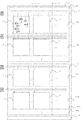
図7は、第2の実施形態に係る固体撮像装置の構成を示す図である。垂直OB画素部2の走査時に同時に選択される3つの画素行のうち、第1の実施形態では常に選択されていた2つの画素行9−n1、9−n2が、第2の実施形態ではNull画素部10の画素行10−1、1−2に置き換えられている。上述のように、Null画素部10内のNull画素はフォトダイオードを有していない点が、開口画素及びOB画素と異なる。垂直OB画素部2及び開口画素部11の読み出しタイミングは、それぞれ図3及び図5と同様である。周辺画素部4及び開口画素部11の回路は、それぞれ図2及び図4と同様である。この構成においても第1の実施形態と同様に補正の基準となる垂直OB画素の出力電圧と開口画素部11の出力差を小さくすることができる。よって、第2の実施形態では、垂直OB画素による出力ばらつきの補正の精度を向上させることができる。これとともに、第1の実施形態と同様の理由により、開口画素部11の混合と同様の混合を垂直OB画素部20において行う場合と比較して、垂直OB画素部20の行数を少なくすることができる。
図8は、第3の実施形態に係る固体撮像装置の構成を示す図である。垂直OB画素部2の走査時に同時に選択される3つの画素行のうち、第1の実施形態では常に選択されていた2つの画素行9−n1、9−n2が、第3の実施形態では、開口画素部11の画素行11−n1、11−n2に置き換えられている。画素行11−n1及び11−n2は、非有効画素として読み出される画素行であり、垂直OB画素部2の近傍に配置される。
図10は、第3の実施形態に係る固体撮像装置の構成を示す図である。図1及び図4に示した第1の実施形態との回路構成上の差異点は、各画素行の入力ノードNFの間に、フローティングディフュージョン(FD)領域間を接続又は非接続とするFD接続トランジスタMeが設けられている点である。図10では、開口画素部11以外の画素部の回路構成が省略されているが、Null画素部10及び垂直OB画素部2にも同様にFD接続トランジスタMeが設けられている。周辺画素部4の回路構成は図2と同様である。開口画素部11−1と開口画素部11−2の間のFD接続トランジスタMeは制御信号φADD1によりオン又はオフに制御される。開口画素部11−2と開口画素部11−3の間のFD接続トランジスタMeは制御信号φADD2により制御される。制御信号φADD3・・・についても同様とする。
図12は、本発明の第5の実施形態に係る固体撮像装置を用いた撮像システムの構成を示す図である。撮像システム800は、光学部810、固体撮像装置820、映像信号処理部830、記録・通信部840、タイミング制御部850、システム制御部860、及び再生・表示部870を備える。固体撮像装置820には、第1〜第4の実施形態として前述した固体撮像装置が用いられる。
2 垂直OB画素部
3 単位画素
10 Null画素部
11 開口画素部
D1、D2 フォトダイオード
Ma 選択トランジスタ
Mb 増幅トランジスタ
Mc リセットトランジスタ
Md1、Md2 転送トランジスタ
Me FD接続トランジスタ
NF 増幅トランジスタの入力ノード(フローティングディフュージョン)
Claims (9)
- 行列状に配置された複数の画素を含む画素アレイと、
前記複数の画素から出力される信号を混合する混合手段とを備える固体撮像装置であって、
前記画素アレイは、
入射された光の光量に依存しない信号を出力する非有効画素を含む第1乃至第3の非有効画素行を有する第1の画素領域と、
入射された光の光量に依存する信号を出力する開口画素を含む複数の有効画素行を有する第2の画素領域と
を備え、
前記混合手段は、
前記第1の非有効画素行の非有効画素から出力される信号と、前記第2の非有効画素行の非有効画素から出力される信号と、を混合した第1の信号と、
前記第1の非有効画素行の非有効画素から出力される信号と、前記第3の非有効画素行の非有効画素から出力される信号と、を混合した第2の信号と、
前記第2の画素領域に含まれる複数の有効画素行の開口画素から出力される信号同士を混合した第3の信号とを生成する
ことを特徴とする固体撮像装置。 - 前記第2及び第3の非有効画素行は、前記非有効画素として、オプティカルブラック画素及びNull画素の少なくとも一方を含むことを特徴とする請求項1に記載の固体撮像装置。
- 前記第1の非有効画素行は、前記非有効画素として、オプティカルブラック画素及びNull画素の少なくとも一方を含むことを特徴とする請求項1又は2に記載の固体撮像装置。
- 前記第1の非有効画素行は、開口画素を含み、
前記第1の非有効画素行は、前記第2の非有効画素行と第3の非有効画素行との間の行に配置されており、
前記混合の際に、前記第1の非有効画素行の開口画素から出力される信号は、入射された光の光量に依存しないことを特徴とする請求項1又は2に記載の固体撮像装置。 - 前記各画素はフローティングディフュージョンを含み、
前記画素アレイはフローティングディフュージョンの間に接続されるトランジスタを含み、前記トランジスタがオンにされることにより、前記フローティングディフュージョンが相互に接続されて信号の混合が行われることを特徴とする請求項1乃至4のいずれか1項に記載の固体撮像装置。 - 前記画素アレイは列に沿った方向に並ぶ各画素に共通に接続される列信号線をさらに備え、
前記複数の画素から信号が前記列信号線に出力されることにより、信号の混合が行われることを特徴とする請求項1乃至4のいずれか1項に記載の固体撮像装置。 - 請求項1乃至6のいずれか1項に記載の固体撮像装置を備えることを特徴とする撮像システム。
- 入射された光の光量に依存しない信号を出力する非有効画素を含む第1乃至第3の非有効画素行を有する第1の画素領域と、入射された光の光量に依存する信号を出力する開口画素を含む複数の有効画素行を有する第2の画素領域とを有する、行列状に配置された複数の画素を含む画素アレイを備える固体撮像装置において、前記複数の画素から出力される信号を混合する方法であって、
前記第1の非有効画素行の非有効画素から出力される信号と、前記第2の非有効画素行の非有効画素から出力される信号と、を混合した第1の信号と、
前記第1の非有効画素行の非有効画素から出力される信号と、前記第3の非有効画素行の非有効画素から出力される信号と、を混合した第2の信号と、
前記第2の画素領域に含まれる複数の有効画素行の開口画素から出力される信号同士を混合した第3の信号とを生成する
ことを特徴とする方法。 - 前記画素アレイは列に沿った方向に並ぶ各画素に共通に接続される列信号線をさらに備え、
前記複数の画素から並行して信号が前記列信号線に出力されることにより、信号の混合が行われる
ことを特徴とする請求項8に記載の方法。
Priority Applications (2)
| Application Number | Priority Date | Filing Date | Title |
|---|---|---|---|
| JP2014095283A JP6385126B2 (ja) | 2014-05-02 | 2014-05-02 | 固体撮像装置 |
| US14/683,595 US9426391B2 (en) | 2014-05-02 | 2015-04-10 | Solid-state imaging apparatus, method of controlling the same, and imaging system |
Applications Claiming Priority (1)
| Application Number | Priority Date | Filing Date | Title |
|---|---|---|---|
| JP2014095283A JP6385126B2 (ja) | 2014-05-02 | 2014-05-02 | 固体撮像装置 |
Publications (3)
| Publication Number | Publication Date |
|---|---|
| JP2015213245A JP2015213245A (ja) | 2015-11-26 |
| JP2015213245A5 JP2015213245A5 (ja) | 2017-06-01 |
| JP6385126B2 true JP6385126B2 (ja) | 2018-09-05 |
Family
ID=54356155
Family Applications (1)
| Application Number | Title | Priority Date | Filing Date |
|---|---|---|---|
| JP2014095283A Active JP6385126B2 (ja) | 2014-05-02 | 2014-05-02 | 固体撮像装置 |
Country Status (2)
| Country | Link |
|---|---|
| US (1) | US9426391B2 (ja) |
| JP (1) | JP6385126B2 (ja) |
Families Citing this family (5)
| Publication number | Priority date | Publication date | Assignee | Title |
|---|---|---|---|---|
| JP7005125B2 (ja) | 2016-04-22 | 2022-01-21 | キヤノン株式会社 | 撮像素子、撮像システム、および撮像素子の製造方法 |
| JP6877203B2 (ja) | 2017-03-24 | 2021-05-26 | キヤノン株式会社 | 撮像装置および移動体 |
| KR20200140284A (ko) | 2018-04-03 | 2020-12-15 | 옵코 아일랜드 글로벌 홀딩스 리미티드 | 비만대사 수술 환자에서의 칼시페디올의 용도 |
| JP7171649B2 (ja) | 2020-05-15 | 2022-11-15 | キヤノン株式会社 | 撮像装置および撮像システム |
| JP7403506B2 (ja) | 2021-08-05 | 2023-12-22 | キヤノン株式会社 | 光電変換装置、撮像装置、機器及び光電変換装置の駆動方法 |
Family Cites Families (10)
| Publication number | Priority date | Publication date | Assignee | Title |
|---|---|---|---|---|
| US7999866B2 (en) * | 2007-05-21 | 2011-08-16 | Canon Kabushiki Kaisha | Imaging apparatus and processing method thereof |
| CN102870404B (zh) * | 2010-10-29 | 2015-03-25 | 富士胶片株式会社 | 摄像设备及其暗电流校正方法 |
| JP5426587B2 (ja) * | 2011-01-31 | 2014-02-26 | 株式会社東芝 | 固体撮像装置及びその画素平均化処理方法 |
| JP5744545B2 (ja) | 2011-01-31 | 2015-07-08 | キヤノン株式会社 | 固体撮像装置およびカメラ |
| JP5871496B2 (ja) * | 2011-06-24 | 2016-03-01 | キヤノン株式会社 | 撮像装置及びその駆動方法 |
| JP5968146B2 (ja) | 2012-07-31 | 2016-08-10 | キヤノン株式会社 | 固体撮像装置およびカメラ |
| JP6216147B2 (ja) | 2013-04-24 | 2017-10-18 | キヤノン株式会社 | 固体撮像装置およびカメラ |
| JP6346479B2 (ja) * | 2013-05-16 | 2018-06-20 | キヤノン株式会社 | 撮像装置、撮像装置の制御方法及びプログラム |
| US10136079B2 (en) * | 2013-10-31 | 2018-11-20 | Ricoh Imaging Company, Ltd. | Method and apparatus for imaging an object |
| JP6294648B2 (ja) | 2013-12-06 | 2018-03-14 | キヤノン株式会社 | 固体撮像装置及びカメラ |
-
2014
- 2014-05-02 JP JP2014095283A patent/JP6385126B2/ja active Active
-
2015
- 2015-04-10 US US14/683,595 patent/US9426391B2/en active Active
Also Published As
| Publication number | Publication date |
|---|---|
| US9426391B2 (en) | 2016-08-23 |
| JP2015213245A (ja) | 2015-11-26 |
| US20150319381A1 (en) | 2015-11-05 |
Similar Documents
| Publication | Publication Date | Title |
|---|---|---|
| TWI726070B (zh) | 固體攝像元件 | |
| US6914227B2 (en) | Image sensing apparatus capable of outputting image by converting resolution by adding and reading out a plurality of pixels, its control method, and image sensing system | |
| JP4827508B2 (ja) | 撮像システム | |
| WO2009096168A1 (ja) | 固体撮像装置およびその駆動方法 | |
| JP6736906B2 (ja) | 固体撮像装置及び画像読み取り装置 | |
| US9627423B2 (en) | Solid-state image pickup apparatus and image pickup system having a clipping circuit arranged close to an N-row signal mixing region | |
| JP6385192B2 (ja) | 撮像装置、撮像システム及び撮像システムの駆動方法 | |
| EP2448254B1 (en) | Solid-state image pickup device | |
| US7486320B2 (en) | Photoelectric conversion device and image pickup system using the photoelectric conversion device | |
| US8023022B2 (en) | Solid-state imaging apparatus | |
| JP6385126B2 (ja) | 固体撮像装置 | |
| JP5322816B2 (ja) | 撮像装置およびその制御方法 | |
| WO2010092651A1 (ja) | 固体撮像装置及び撮像装置 | |
| EP3468170B1 (en) | Solid-state imaging element and imaging apparatus | |
| US9800810B2 (en) | Imaging apparatus and imaging system | |
| WO2012144218A1 (ja) | 固体撮像装置および固体撮像装置の駆動方法 | |
| JP6000589B2 (ja) | 固体撮像装置 | |
| US9807329B2 (en) | Imaging device and imaging system | |
| JP2009290296A (ja) | 撮像装置 | |
| JP6532224B2 (ja) | 撮像装置、撮像システム、及び撮像装置の駆動方法 | |
| JP4347820B2 (ja) | 撮像装置 | |
| JP6809526B2 (ja) | 撮像素子および撮像装置 | |
| JP6555979B2 (ja) | 撮像装置、撮像システム | |
| JP2009177542A (ja) | 固体撮像装置および撮像機器 | |
| JP2018152649A (ja) | 固体撮像装置及び固体撮像装置の駆動方法 |
Legal Events
| Date | Code | Title | Description |
|---|---|---|---|
| A521 | Request for written amendment filed |
Free format text: JAPANESE INTERMEDIATE CODE: A523 Effective date: 20170412 |
|
| A621 | Written request for application examination |
Free format text: JAPANESE INTERMEDIATE CODE: A621 Effective date: 20170412 |
|
| RD05 | Notification of revocation of power of attorney |
Free format text: JAPANESE INTERMEDIATE CODE: A7425 Effective date: 20171214 |
|
| RD04 | Notification of resignation of power of attorney |
Free format text: JAPANESE INTERMEDIATE CODE: A7424 Effective date: 20180126 |
|
| A977 | Report on retrieval |
Free format text: JAPANESE INTERMEDIATE CODE: A971007 Effective date: 20180302 |
|
| A131 | Notification of reasons for refusal |
Free format text: JAPANESE INTERMEDIATE CODE: A131 Effective date: 20180306 |
|
| A521 | Request for written amendment filed |
Free format text: JAPANESE INTERMEDIATE CODE: A523 Effective date: 20180502 |
|
| TRDD | Decision of grant or rejection written | ||
| A01 | Written decision to grant a patent or to grant a registration (utility model) |
Free format text: JAPANESE INTERMEDIATE CODE: A01 Effective date: 20180710 |
|
| A61 | First payment of annual fees (during grant procedure) |
Free format text: JAPANESE INTERMEDIATE CODE: A61 Effective date: 20180807 |
|
| R151 | Written notification of patent or utility model registration |
Ref document number: 6385126 Country of ref document: JP Free format text: JAPANESE INTERMEDIATE CODE: R151 |