JP6313076B2 - スピン軌道相互作用基礎のスイッチングを利用する磁気トンネル接合を含む磁気メモリ構造 - Google Patents
スピン軌道相互作用基礎のスイッチングを利用する磁気トンネル接合を含む磁気メモリ構造 Download PDFInfo
- Publication number
- JP6313076B2 JP6313076B2 JP2014051606A JP2014051606A JP6313076B2 JP 6313076 B2 JP6313076 B2 JP 6313076B2 JP 2014051606 A JP2014051606 A JP 2014051606A JP 2014051606 A JP2014051606 A JP 2014051606A JP 6313076 B2 JP6313076 B2 JP 6313076B2
- Authority
- JP
- Japan
- Prior art keywords
- magnetic
- memory
- spin
- current
- active layer
- Prior art date
- Legal status (The legal status is an assumption and is not a legal conclusion. Google has not performed a legal analysis and makes no representation as to the accuracy of the status listed.)
- Active
Links
- 230000005291 magnetic effect Effects 0.000 title claims description 412
- 230000015654 memory Effects 0.000 title claims description 382
- 230000003993 interaction Effects 0.000 title claims description 122
- 210000004027 cell Anatomy 0.000 claims description 65
- 210000000352 storage cell Anatomy 0.000 claims description 53
- 101100167360 Drosophila melanogaster chb gene Proteins 0.000 claims description 36
- 238000000034 method Methods 0.000 claims description 23
- 230000002457 bidirectional effect Effects 0.000 claims description 9
- 238000013500 data storage Methods 0.000 claims description 7
- 238000003491 array Methods 0.000 claims description 6
- 230000000694 effects Effects 0.000 description 61
- 238000010586 diagram Methods 0.000 description 56
- 230000008878 coupling Effects 0.000 description 17
- 238000010168 coupling process Methods 0.000 description 17
- 238000005859 coupling reaction Methods 0.000 description 17
- 239000000463 material Substances 0.000 description 10
- 230000007246 mechanism Effects 0.000 description 9
- 230000003213 activating effect Effects 0.000 description 7
- 230000004888 barrier function Effects 0.000 description 7
- 230000005355 Hall effect Effects 0.000 description 6
- 229910052737 gold Inorganic materials 0.000 description 6
- 230000010354 integration Effects 0.000 description 6
- 229910052697 platinum Inorganic materials 0.000 description 6
- 229910052725 zinc Inorganic materials 0.000 description 6
- 229910052789 astatine Inorganic materials 0.000 description 5
- 229910052802 copper Inorganic materials 0.000 description 5
- 229910052745 lead Inorganic materials 0.000 description 5
- 229910052753 mercury Inorganic materials 0.000 description 5
- 229910052763 palladium Inorganic materials 0.000 description 5
- 229910052702 rhenium Inorganic materials 0.000 description 5
- 229910052709 silver Inorganic materials 0.000 description 5
- 229910052715 tantalum Inorganic materials 0.000 description 5
- 229910052721 tungsten Inorganic materials 0.000 description 5
- 230000005290 antiferromagnetic effect Effects 0.000 description 4
- 229910052793 cadmium Inorganic materials 0.000 description 4
- 238000005090 crystal field Methods 0.000 description 4
- 238000013016 damping Methods 0.000 description 4
- 229910052733 gallium Inorganic materials 0.000 description 4
- 229910052741 iridium Inorganic materials 0.000 description 4
- 230000005415 magnetization Effects 0.000 description 4
- 229910052750 molybdenum Inorganic materials 0.000 description 4
- 229910052758 niobium Inorganic materials 0.000 description 4
- 229910052762 osmium Inorganic materials 0.000 description 4
- 230000002829 reductive effect Effects 0.000 description 4
- 229910052703 rhodium Inorganic materials 0.000 description 4
- 229910052707 ruthenium Inorganic materials 0.000 description 4
- 229910052713 technetium Inorganic materials 0.000 description 4
- 229910052716 thallium Inorganic materials 0.000 description 4
- 229910052726 zirconium Inorganic materials 0.000 description 4
- 229910052684 Cerium Inorganic materials 0.000 description 3
- 229910052692 Dysprosium Inorganic materials 0.000 description 3
- 229910052693 Europium Inorganic materials 0.000 description 3
- 229910052688 Gadolinium Inorganic materials 0.000 description 3
- 229910052689 Holmium Inorganic materials 0.000 description 3
- 241000592718 Ibla Species 0.000 description 3
- 229910052779 Neodymium Inorganic materials 0.000 description 3
- 229910052777 Praseodymium Inorganic materials 0.000 description 3
- 229910052772 Samarium Inorganic materials 0.000 description 3
- 229910052771 Terbium Inorganic materials 0.000 description 3
- 229910052769 Ytterbium Inorganic materials 0.000 description 3
- 229910052785 arsenic Inorganic materials 0.000 description 3
- 230000008901 benefit Effects 0.000 description 3
- 229910052804 chromium Inorganic materials 0.000 description 3
- 230000001351 cycling effect Effects 0.000 description 3
- 230000007423 decrease Effects 0.000 description 3
- 230000009977 dual effect Effects 0.000 description 3
- 229910052732 germanium Inorganic materials 0.000 description 3
- 229910001385 heavy metal Inorganic materials 0.000 description 3
- 229910052738 indium Inorganic materials 0.000 description 3
- 229910052746 lanthanum Inorganic materials 0.000 description 3
- 230000001151 other effect Effects 0.000 description 3
- 229910052710 silicon Inorganic materials 0.000 description 3
- 229910052691 Erbium Inorganic materials 0.000 description 2
- 229910052775 Thulium Inorganic materials 0.000 description 2
- 238000009825 accumulation Methods 0.000 description 2
- 229910045601 alloy Inorganic materials 0.000 description 2
- 239000000956 alloy Substances 0.000 description 2
- 230000005294 ferromagnetic effect Effects 0.000 description 2
- 230000006870 function Effects 0.000 description 2
- 229910052742 iron Inorganic materials 0.000 description 2
- 239000000696 magnetic material Substances 0.000 description 2
- 229910052748 manganese Inorganic materials 0.000 description 2
- 230000007334 memory performance Effects 0.000 description 2
- 239000000203 mixture Substances 0.000 description 2
- 229910052759 nickel Inorganic materials 0.000 description 2
- 230000036961 partial effect Effects 0.000 description 2
- 230000005641 tunneling Effects 0.000 description 2
- 229910052720 vanadium Inorganic materials 0.000 description 2
- 101100232386 Arabidopsis thaliana IBL1 gene Proteins 0.000 description 1
- -1 GaMn Inorganic materials 0.000 description 1
- 229910001218 Gallium arsenide Inorganic materials 0.000 description 1
- 229910000530 Gallium indium arsenide Inorganic materials 0.000 description 1
- 102100030385 Granzyme B Human genes 0.000 description 1
- 101001009603 Homo sapiens Granzyme B Proteins 0.000 description 1
- 229910052765 Lutetium Inorganic materials 0.000 description 1
- 229910000661 Mercury cadmium telluride Inorganic materials 0.000 description 1
- 230000004913 activation Effects 0.000 description 1
- 229910052782 aluminium Inorganic materials 0.000 description 1
- 229910052787 antimony Inorganic materials 0.000 description 1
- 239000000969 carrier Substances 0.000 description 1
- 230000008859 change Effects 0.000 description 1
- 239000002800 charge carrier Substances 0.000 description 1
- 239000004020 conductor Substances 0.000 description 1
- 239000013078 crystal Substances 0.000 description 1
- 230000003247 decreasing effect Effects 0.000 description 1
- 230000005347 demagnetization Effects 0.000 description 1
- 230000001419 dependent effect Effects 0.000 description 1
- 238000005516 engineering process Methods 0.000 description 1
- 230000001747 exhibiting effect Effects 0.000 description 1
- 229910052735 hafnium Inorganic materials 0.000 description 1
- WPYVAWXEWQSOGY-UHFFFAOYSA-N indium antimonide Chemical compound [Sb]#[In] WPYVAWXEWQSOGY-UHFFFAOYSA-N 0.000 description 1
- 230000001939 inductive effect Effects 0.000 description 1
- 239000012212 insulator Substances 0.000 description 1
- 230000002452 interceptive effect Effects 0.000 description 1
- 230000000873 masking effect Effects 0.000 description 1
- 239000011159 matrix material Substances 0.000 description 1
- TWNQGVIAIRXVLR-UHFFFAOYSA-N oxo(oxoalumanyloxy)alumane Chemical compound O=[Al]O[Al]=O TWNQGVIAIRXVLR-UHFFFAOYSA-N 0.000 description 1
- 230000003071 parasitic effect Effects 0.000 description 1
- 229910052698 phosphorus Inorganic materials 0.000 description 1
- 230000010287 polarization Effects 0.000 description 1
- 230000009467 reduction Effects 0.000 description 1
- 239000004065 semiconductor Substances 0.000 description 1
- 229910052717 sulfur Inorganic materials 0.000 description 1
- 229910052719 titanium Inorganic materials 0.000 description 1
- 229910052727 yttrium Inorganic materials 0.000 description 1
Images


Classifications
-
- G—PHYSICS
- G11—INFORMATION STORAGE
- G11C—STATIC STORES
- G11C11/00—Digital stores characterised by the use of particular electric or magnetic storage elements; Storage elements therefor
- G11C11/02—Digital stores characterised by the use of particular electric or magnetic storage elements; Storage elements therefor using magnetic elements
- G11C11/16—Digital stores characterised by the use of particular electric or magnetic storage elements; Storage elements therefor using magnetic elements using elements in which the storage effect is based on magnetic spin effect
- G11C11/165—Auxiliary circuits
- G11C11/1673—Reading or sensing circuits or methods
-
- G—PHYSICS
- G11—INFORMATION STORAGE
- G11C—STATIC STORES
- G11C11/00—Digital stores characterised by the use of particular electric or magnetic storage elements; Storage elements therefor
- G11C11/02—Digital stores characterised by the use of particular electric or magnetic storage elements; Storage elements therefor using magnetic elements
- G11C11/16—Digital stores characterised by the use of particular electric or magnetic storage elements; Storage elements therefor using magnetic elements using elements in which the storage effect is based on magnetic spin effect
- G11C11/161—Digital stores characterised by the use of particular electric or magnetic storage elements; Storage elements therefor using magnetic elements using elements in which the storage effect is based on magnetic spin effect details concerning the memory cell structure, e.g. the layers of the ferromagnetic memory cell
-
- G—PHYSICS
- G11—INFORMATION STORAGE
- G11C—STATIC STORES
- G11C11/00—Digital stores characterised by the use of particular electric or magnetic storage elements; Storage elements therefor
- G11C11/02—Digital stores characterised by the use of particular electric or magnetic storage elements; Storage elements therefor using magnetic elements
- G11C11/16—Digital stores characterised by the use of particular electric or magnetic storage elements; Storage elements therefor using magnetic elements using elements in which the storage effect is based on magnetic spin effect
- G11C11/165—Auxiliary circuits
- G11C11/1653—Address circuits or decoders
-
- G—PHYSICS
- G11—INFORMATION STORAGE
- G11C—STATIC STORES
- G11C11/00—Digital stores characterised by the use of particular electric or magnetic storage elements; Storage elements therefor
- G11C11/02—Digital stores characterised by the use of particular electric or magnetic storage elements; Storage elements therefor using magnetic elements
- G11C11/16—Digital stores characterised by the use of particular electric or magnetic storage elements; Storage elements therefor using magnetic elements using elements in which the storage effect is based on magnetic spin effect
- G11C11/165—Auxiliary circuits
- G11C11/1659—Cell access
-
- G—PHYSICS
- G11—INFORMATION STORAGE
- G11C—STATIC STORES
- G11C11/00—Digital stores characterised by the use of particular electric or magnetic storage elements; Storage elements therefor
- G11C11/02—Digital stores characterised by the use of particular electric or magnetic storage elements; Storage elements therefor using magnetic elements
- G11C11/16—Digital stores characterised by the use of particular electric or magnetic storage elements; Storage elements therefor using magnetic elements using elements in which the storage effect is based on magnetic spin effect
- G11C11/165—Auxiliary circuits
- G11C11/1675—Writing or programming circuits or methods
-
- G—PHYSICS
- G11—INFORMATION STORAGE
- G11C—STATIC STORES
- G11C11/00—Digital stores characterised by the use of particular electric or magnetic storage elements; Storage elements therefor
- G11C11/18—Digital stores characterised by the use of particular electric or magnetic storage elements; Storage elements therefor using Hall-effect devices
Landscapes
- Engineering & Computer Science (AREA)
- Computer Hardware Design (AREA)
- Hall/Mr Elements (AREA)
- Mram Or Spin Memory Techniques (AREA)
Description
12・・・従来のシード層
14・・・従来の反強磁性層
16・・・従来の固定層
18・・・従来のトンネルバリアー層
20・・・従来の自由層
22・・・従来のキャッピング層
24・・・従来の上部コンタクト
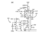
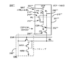
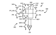
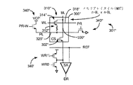
122・・・SO活性層
112・・・データ格納層/自由層
114・・・非磁気空間層
116・・・基準層
173・・・駆動/感知回路
175・・・書込み回路
177・・・読出し回路
179・・・中間デコーディング回路
Claims (10)
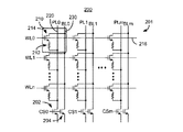
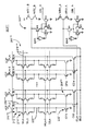
- 複数のメモリアレイタイル(MATs)と、
前記複数のメモリアレイタイルと共に読出し動作及び書込み動作を制御する中間回路と、
前記複数のメモリアレイタイルの一部分に各々対応する複数のグローバルビットラインと、
前記読出し動作及び前記書込み動作のために前記複数のグローバルビットラインの一部分を選択し、駆動するグローバル回路と、を含み、
前記複数のメモリアレイタイルは、各々複数のビットライン、複数のワードライン、及び複数の磁気格納セルを含み、
前記複数の磁気格納セルの各々は、少なくとも1つの磁気接合、少なくとも1つの選択装置、及び前記少なくとも1つの磁気接合に隣接するスピン軌道SO相互作用活性層の少なくとも一部を含み、
前記スピン軌道SO相互作用活性層の少なくとも一部には少なくとも1つのスピン軌道電流を前記スピン軌道SO相互作用活性層の少なくとも一部分を通じて通過させることによって、スピン軌道トルクが加えられ、
前記少なくとも1つの磁気接合は、前記少なくとも1つの磁気接合を通じて駆動された少なくとも1つの書込み電流及び前記スピン軌道SO相互作用活性層の少なくとも一部に提供される少なくとも1つのスピン軌道電流を利用してプログラムされ、
前記複数のビットライン及び前記複数のワードラインは、前記複数の磁気メモリセルに対応する磁気メモリ。 - 前記少なくとも1つの磁気接合は、各々基準層、非磁気空間層、及び自由層を含み、
前記自由層は、磁気的であり、
前記非磁気空間層は、前記基準層及び前記自由層の間に位置し、
前記スピン軌道SO相互作用活性層の少なくとも一部は、前記自由層に隣接する請求項1に記載の磁気メモリ。 - 前記メモリアレイタイルの各々は、複数の共通バスを含み、
前記複数の共通バスの各々は、複数の磁気接合の各々に接続され、前記スピン軌道SO相互作用活性層の一部を含み、前記スピン軌道電流を伝送する請求項1に記載の磁気メモリ。 - 前記スピン軌道電流は、プリコンディショニング(preconditioning)電流である請求項3に記載の磁気メモリ。
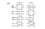
- 前記プリコンディショニング電流は、複数の磁気接合の各々に書き込まれるデータに依存する方向を有する両方向電流である請求項4に記載の磁気メモリ。
- 前記プリコンディショニング電流は、一方向電流である請求項4に記載の磁気メモリ。
- 前記複数の共通バスは、複数のソースラインに対応し、
前記複数のワードラインは、各々、前記複数の磁気格納セルの各々に含まれる前記少なくとも1つの選択装置を介して、前記複数のビットラインの各々に接続された請求項3に記載の磁気メモリ。 - 複数のメモリアレイタイルと、
少なくとも1つの磁気接合と、
中間回路と、
複数のグローバルビットラインと、
グローバル回路と、を含み、
前記複数のメモリアレイタイルの各々は、複数の磁気格納セル、複数のビットライン、複数のワードライン、及びプリコンディショニング(preconditioning)電流を伝送するための複数の共通バスを含み、
前記複数の磁気格納セルの各々は、少なくとも1つの磁気接合、少なくとも1つの選択装置、及び前記少なくとも1つの磁気接合に隣接するスピン軌道相互作用SO活性層を含み、
前記スピン軌道相互作用SO活性層の少なくとも一部は、前記プリコンディショニング電流を前記スピン軌道相互作用SO活性層の前記少なくとも一部を通じて通過させることによって、前記少なくとも1つの磁気接合にスピン軌道相互作用を加え、
前記複数の共通バスの各々は、前記複数の磁気接合の一部と接続され、前記プリコンディショニング電流を通過させるために前記スピン軌道相互作用SO活性層の前記一部を含み、
プログラム可能である前記少なくとも1つの磁気接合は、前記少なくとも1つの磁気接合を通じて駆動される少なくとも1つの書込み電流及び前記スピン軌道相互作用SO活性層の前記少なくとも一部に提供される前記プリコンディショニング電流を利用し、
前記複数のビットライン及び前記複数のワードラインは、前記複数の磁気格納セルに対応し、
前記中間回路は、前記複数のメモリアレイタイルでの読出し動作及び書込み動作を制御し、前記中間回路は、中間駆動及び感知回路とローカルデコーディング回路とをさらに含み、
前記複数のグローバルビットラインの各々は、前記複数のメモリアレイタイルの一部に対応し、前記複数のグローバルビットラインは、第1抵抗を有し、前記複数のワードライ
ンは、第2抵抗を有し、前記複数のビットラインは、第3抵抗を有し、前記第1抵抗は、前記第2及び第3抵抗より小さく、
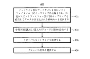
前記グローバル回路は、読出し動作及び書込み動作のために前記複数のグローバルビットラインの一部を選択し、駆動する磁気メモリ。 - 複数のメモリアレイタイルを提供する段階と、
前記複数のメモリアレイタイルでの読出し動作及び書込み動作を制御するために中間回路を提供する段階と、
各々前記複数のメモリアレイタイルに対する複数のグローバルビットラインを提供する段階と、
前記読出し動作及び前記書込み動作のために前記複数のグローバルビットラインの一部を選択し、駆動するグローバル回路を提供する段階と、を含み、
前記複数のメモリアレイタイルの各々は、複数のビットライン、複数のワードライン、及び複数の磁気格納セルを含み、
前記複数の磁気格納セルの各々は、少なくとも1つの磁気接合、少なくとも1つの選択装置及び前記少なくとも1つの磁気接合に隣接するスピン軌道相互作用SO活性層を含み、
前記スピン軌道相互作用SO活性層の少なくとも一部は、スピン軌道相互作用電流を前記スピン軌道相互作用SO活性層の前記少なくとも一部を通じて通過させることによって、前記少なくとも1つの磁気接合の一部にスピン軌道相互作用トルクを加え、
プログラム可能である前記少なくとも1つの磁気接合は、前記少なくとも1つの磁気接合を通じて駆動される少なくとも1つの書込み電流及び前記スピン軌道相互作用SO活性層の前記少なくとも一部に提供される前記スピン軌道相互作用電流を利用し、
前記複数のビットライン及び前記複数のワードラインは、前記複数の磁気格納セルに対応する磁気メモリを提供する方法。 - 複数の磁気接合を含む磁気メモリのプログラム方法において、
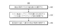
前記複数の磁気接合の各々は、磁化可能であるデータ格納層を含み、前記方法は、
複数のメモリアレイタイルの中で少なくとも1つのメモリアレイタイル内の複数の共通バスの中で少なくとも1つの共通バスを通じてプリチャージ電流を駆動する段階と、
少なくとも1つの選択された磁気メモリセルの少なくとも1つの磁気接合を通じて少なくとも1つの書込み電流を駆動する段階と、を含み、
前記複数のメモリアレイ他これらの各々は、複数の共通バス、複数のビットライン、複数のワードライン、及び複数の磁気格納セルを含み、
前記複数の共通バスの各々は、前記磁気接合に隣接する少なくとも1つのスピン軌道相互作用活性層を含み、
前記複数の磁気格納セルの各々は、少なくとも1つの磁気接合、少なくとも1つの選択装置、及び前記磁気接合に隣接するスピン軌道相互作用活性層の少なくとも一部を含み、
前記スピン軌道相互作用SO活性層の少なくとも一部は、プリコンディショニング電流を前記スピン軌道相互作用SO活性層の前記少なくとも一部を通じて通過させることによって、前記磁気接合の少なくとも一部にスピン軌道相互作用トルクを加え、
プログラム可能である前記少なくとも1つの磁気接合は、前記少なくとも1つの磁気接合を通じて駆動される少なくとも1つの書込み電流及び前記スピン軌道相互作用SO活性層の前記少なくとも一部に提供される前記プリコンディショニング電流を利用し、
前記複数のビットライン及び前記複数のワードラインは、前記複数の磁気格納セルに対応し、
前記複数の共通バスの中で前記少なくとも1つの共通バスは、前記複数の磁気格納セルの中で前記少なくとも1つの選択された磁気格納セルに対応する磁気メモリのプログラム方法。
Applications Claiming Priority (6)
| Application Number | Priority Date | Filing Date | Title |
|---|---|---|---|
| US201361785908P | 2013-03-14 | 2013-03-14 | |
| US61/785,908 | 2013-03-14 | ||
| US201361798578P | 2013-03-15 | 2013-03-15 | |
| US61/798,578 | 2013-03-15 | ||
| US13/851,274 | 2013-03-27 | ||
| US13/851,274 US9076541B2 (en) | 2013-03-14 | 2013-03-27 | Architecture for magnetic memories including magnetic tunneling junctions using spin-orbit interaction based switching |
Publications (3)
| Publication Number | Publication Date |
|---|---|
| JP2014179618A JP2014179618A (ja) | 2014-09-25 |
| JP2014179618A5 JP2014179618A5 (ja) | 2017-04-06 |
| JP6313076B2 true JP6313076B2 (ja) | 2018-04-18 |
Family
ID=51419114
Family Applications (1)
| Application Number | Title | Priority Date | Filing Date |
|---|---|---|---|
| JP2014051606A Active JP6313076B2 (ja) | 2013-03-14 | 2014-03-14 | スピン軌道相互作用基礎のスイッチングを利用する磁気トンネル接合を含む磁気メモリ構造 |
Country Status (5)
| Country | Link |
|---|---|
| US (1) | US9076541B2 (ja) |
| JP (1) | JP6313076B2 (ja) |
| KR (1) | KR102175859B1 (ja) |
| CN (1) | CN104050988B (ja) |
| DE (1) | DE102014103276A1 (ja) |
Families Citing this family (27)
| Publication number | Priority date | Publication date | Assignee | Title |
|---|---|---|---|---|
| US9384812B2 (en) * | 2014-01-28 | 2016-07-05 | Qualcomm Incorporated | Three-phase GSHE-MTJ non-volatile flip-flop |
| US9251883B2 (en) * | 2014-01-28 | 2016-02-02 | Qualcomm Incorporated | Single phase GSHE-MTJ non-volatile flip-flop |
| US10008248B2 (en) | 2014-07-17 | 2018-06-26 | Cornell University | Circuits and devices based on enhanced spin hall effect for efficient spin transfer torque |
| CN104866390B (zh) * | 2015-04-15 | 2018-07-20 | 中国科学院高能物理研究所 | 异步随机静态存储器三模冗余控制器 |
| US10333523B2 (en) * | 2015-05-28 | 2019-06-25 | Intel Corporation | Exclusive-OR logic device with spin orbit torque effect |
| US9997564B2 (en) | 2015-10-09 | 2018-06-12 | Western Digital Technologies, Inc. | MTJ memory array subgrouping method and related drive circuitry |
| KR102477093B1 (ko) * | 2015-10-13 | 2022-12-13 | 삼성전자주식회사 | 푸리에 변환을 수행하는 방법 및 장치 |
| US9768229B2 (en) | 2015-10-22 | 2017-09-19 | Western Digital Technologies, Inc. | Bottom pinned SOT-MRAM bit structure and method of fabrication |
| US10305026B2 (en) | 2015-11-19 | 2019-05-28 | Samsung Electronics Co., Ltd. | Cross-point architecture for spin-transfer torque magnetoresistive random access memory with spin orbit writing |
| US10586916B2 (en) | 2015-11-27 | 2020-03-10 | Tdk Corporation | Spin current magnetization reversal element, magnetoresistance effect element, and magnetic memory |
| CN105390609A (zh) * | 2015-12-01 | 2016-03-09 | 中电海康集团有限公司 | 一种自旋霍尔效应辅助的磁性随机存储器 |
| JP6833810B2 (ja) * | 2016-03-14 | 2021-02-24 | Tdk株式会社 | 磁気メモリ |
| JP6271655B1 (ja) * | 2016-08-05 | 2018-01-31 | 株式会社東芝 | 不揮発性メモリ |
| JP6271654B1 (ja) | 2016-08-05 | 2018-01-31 | 株式会社東芝 | 不揮発性メモリ |
| US9875780B1 (en) * | 2016-08-30 | 2018-01-23 | International Business Machines Corporation | STT MRAM source line configuration |
| US10236046B2 (en) * | 2016-11-09 | 2019-03-19 | Imec Vzw | Method of propagating magnetic domain wall in magnetic devices |
| KR102522620B1 (ko) * | 2016-11-29 | 2023-04-19 | 삼성전자주식회사 | 자기 메모리 소자 및 자기 메모리 소자의 쓰기 방법 |
| US11107615B2 (en) * | 2017-02-24 | 2021-08-31 | Tdk Corporation | Magnetization rotational element, magnetoresistance effect element, and memory device |
| JP6290487B1 (ja) | 2017-03-17 | 2018-03-07 | 株式会社東芝 | 磁気メモリ |
| JP6316474B1 (ja) * | 2017-03-21 | 2018-04-25 | 株式会社東芝 | 磁気メモリ |
| JP6815297B2 (ja) * | 2017-09-15 | 2021-01-20 | 株式会社東芝 | 磁気メモリ |
| US11290110B2 (en) * | 2017-10-26 | 2022-03-29 | Samsung Electronics Co., Ltd. | Method and system for providing a variation resistant magnetic junction-based XNOR cell usable in neuromorphic computing |
| US10431291B1 (en) * | 2018-08-08 | 2019-10-01 | Micron Technology, Inc. | Systems and methods for dynamic random access memory (DRAM) cell voltage boosting |
| WO2020157958A1 (ja) * | 2019-02-01 | 2020-08-06 | Tdk株式会社 | スピン軌道トルク型磁気抵抗効果素子及び磁気メモリ |
| CN112151089B (zh) * | 2019-06-28 | 2022-09-30 | 中电海康集团有限公司 | 存储器 |
| KR20210020482A (ko) | 2019-08-14 | 2021-02-24 | 삼성전자주식회사 | 자기 메모리 장치 |
| CN113451503B (zh) * | 2020-12-31 | 2023-03-17 | 北京航空航天大学 | 多功能磁性随机存储单元、存储器及设备 |
Family Cites Families (26)
| Publication number | Priority date | Publication date | Assignee | Title |
|---|---|---|---|---|
| US6081445A (en) | 1998-07-27 | 2000-06-27 | Motorola, Inc. | Method to write/read MRAM arrays |
| DE10060432A1 (de) | 2000-12-05 | 2002-07-25 | Infineon Technologies Ag | Magnetoresistiver Speicher und Verfahren zu seinem Auslesen |
| US6738303B1 (en) | 2002-11-27 | 2004-05-18 | Motorola, Inc. | Technique for sensing the state of a magneto-resistive random access memory |
| US8755222B2 (en) * | 2003-08-19 | 2014-06-17 | New York University | Bipolar spin-transfer switching |
| US7154798B2 (en) | 2004-04-27 | 2006-12-26 | Taiwan Semiconductor Manufacturing Company, Ltd. | MRAM arrays and methods for writing and reading magnetic memory devices |
| US7038959B2 (en) | 2004-09-17 | 2006-05-02 | Freescale Semiconductor, Inc. | MRAM sense amplifier having a precharge circuit and method for sensing |
| JP4779608B2 (ja) | 2005-11-30 | 2011-09-28 | Tdk株式会社 | 磁気メモリ |
| US8508984B2 (en) * | 2006-02-25 | 2013-08-13 | Avalanche Technology, Inc. | Low resistance high-TMR magnetic tunnel junction and process for fabrication thereof |
| US7848059B2 (en) * | 2006-09-29 | 2010-12-07 | Kabushiki Kaisha Toshiba | Magnetoresistive effect device and magnetic random access memory using the same |
| JP4934582B2 (ja) * | 2007-12-25 | 2012-05-16 | 株式会社日立製作所 | スピンホール効果素子を用いた磁気センサ、磁気ヘッド及び磁気メモリ |
| US7813168B2 (en) | 2008-10-27 | 2010-10-12 | Seagate Technology Llc | Spin-transfer torque memory self-reference read and write assist methods |
| CN101770804B (zh) * | 2009-01-06 | 2012-12-12 | 中国科学院物理研究所 | 一种磁性随机存储器、磁性逻辑器件和自旋微波振荡器 |
| JP4901899B2 (ja) | 2009-03-30 | 2012-03-21 | 株式会社東芝 | 磁気抵抗効果メモリ |
| US8385106B2 (en) * | 2009-09-11 | 2013-02-26 | Grandis, Inc. | Method and system for providing a hierarchical data path for spin transfer torque random access memory |
| US8064246B2 (en) * | 2009-12-10 | 2011-11-22 | John Casimir Slonczewski | Creating spin-transfer torque in oscillators and memories |
| FR2963152B1 (fr) * | 2010-07-26 | 2013-03-29 | Centre Nat Rech Scient | Element de memoire magnetique |
| FR2963153B1 (fr) * | 2010-07-26 | 2013-04-26 | Centre Nat Rech Scient | Element magnetique inscriptible |
| FR2966636B1 (fr) * | 2010-10-26 | 2012-12-14 | Centre Nat Rech Scient | Element magnetique inscriptible |
| US9082497B2 (en) * | 2011-03-22 | 2015-07-14 | Renesas Electronics Corporation | Magnetic memory using spin orbit interaction |
| JP5761788B2 (ja) * | 2011-03-25 | 2015-08-12 | 株式会社東芝 | 磁気抵抗素子および磁気メモリ |
| KR101912223B1 (ko) * | 2011-08-16 | 2019-01-04 | 삼성전자주식회사 | 적층 자기 램 장치 및 이를 포함하는 메모리 시스템 |
| KR101457511B1 (ko) * | 2011-08-18 | 2014-11-04 | 코넬 유니버시티 | 스핀 홀 효과 자기 장치, 방법, 및 적용 |
| WO2013062617A1 (en) * | 2011-10-25 | 2013-05-02 | Massachusetts Institute Of Technology | High density molecular memory storage with read and write capabilites |
| JP2013115400A (ja) * | 2011-12-01 | 2013-06-10 | Sony Corp | 記憶素子、記憶装置 |
| JP5499264B2 (ja) * | 2012-03-21 | 2014-05-21 | 株式会社東芝 | 磁気抵抗素子および磁気メモリ |
| US8860156B2 (en) * | 2012-09-11 | 2014-10-14 | Headway Technologies, Inc. | Minimal thickness synthetic antiferromagnetic (SAF) structure with perpendicular magnetic anisotropy for STT-MRAM |
-
2013
- 2013-03-27 US US13/851,274 patent/US9076541B2/en active Active
-
2014
- 2014-03-12 DE DE102014103276.4A patent/DE102014103276A1/de active Pending
- 2014-03-12 KR KR1020140029118A patent/KR102175859B1/ko active IP Right Grant
- 2014-03-14 JP JP2014051606A patent/JP6313076B2/ja active Active
- 2014-03-14 CN CN201410095613.8A patent/CN104050988B/zh active Active
Also Published As
| Publication number | Publication date |
|---|---|
| CN104050988B (zh) | 2018-08-28 |
| US20140269032A1 (en) | 2014-09-18 |
| DE102014103276A1 (de) | 2014-09-18 |
| US9076541B2 (en) | 2015-07-07 |
| JP2014179618A (ja) | 2014-09-25 |
| KR102175859B1 (ko) | 2020-11-09 |
| CN104050988A (zh) | 2014-09-17 |
| KR20150048612A (ko) | 2015-05-07 |
Similar Documents
| Publication | Publication Date | Title |
|---|---|---|
| JP6313076B2 (ja) | スピン軌道相互作用基礎のスイッチングを利用する磁気トンネル接合を含む磁気メモリ構造 | |
| US7800942B2 (en) | Method and system for providing a magnetic element and magnetic memory being unidirectional writing enabled | |
| KR102534007B1 (ko) | 스핀 궤도 쓰기를 갖는 스핀 전달 토크 자기저항 랜덤 액세스 메모리를 위한 크로스 포인트 구조 | |
| JP3920564B2 (ja) | 磁気ランダムアクセスメモリ | |
| KR100520865B1 (ko) | 2방향의 데이터 기입 자계에 의해 데이터 기입을 실행하는박막 자성체 기억 장치 | |
| US7852662B2 (en) | Spin-torque MRAM: spin-RAM, array | |
| US9129692B1 (en) | High density magnetic random access memory | |
| US20120281465A1 (en) | High Density Magnetic Random Access Memory | |
| US20160155486A1 (en) | Resistance change memory | |
| US8466524B2 (en) | Static magnetic field assisted resistive sense element | |
| JP2002343077A (ja) | 薄膜磁性体記憶装置 | |
| KR20190029407A (ko) | 반도체 장치 및 이의 제조 방법 | |
| CN101625890A (zh) | 操作磁随机存取存储器装置的方法 | |
| US8411497B2 (en) | Method and system for providing a magnetic field aligned spin transfer torque random access memory | |
| US10573363B2 (en) | Method and apparatus for performing self-referenced read in a magnetoresistive random access memory | |
| US10854262B2 (en) | Memory device | |
| JP2007122838A (ja) | 半導体記憶装置 | |
| JP4553927B2 (ja) | 半導体装置 | |
| JP4675362B2 (ja) | 半導体装置 | |
| JP5005070B2 (ja) | 半導体装置 | |
| JP5140859B2 (ja) | 半導体装置 |
Legal Events
| Date | Code | Title | Description |
|---|---|---|---|
| RD04 | Notification of resignation of power of attorney |
Free format text: JAPANESE INTERMEDIATE CODE: A7424 Effective date: 20141226 |
|
| A521 | Request for written amendment filed |
Free format text: JAPANESE INTERMEDIATE CODE: A523 Effective date: 20170301 |
|
| A621 | Written request for application examination |
Free format text: JAPANESE INTERMEDIATE CODE: A621 Effective date: 20170301 |
|
| A131 | Notification of reasons for refusal |
Free format text: JAPANESE INTERMEDIATE CODE: A131 Effective date: 20171113 |
|
| A521 | Request for written amendment filed |
Free format text: JAPANESE INTERMEDIATE CODE: A523 Effective date: 20180118 |
|
| TRDD | Decision of grant or rejection written | ||
| A01 | Written decision to grant a patent or to grant a registration (utility model) |
Free format text: JAPANESE INTERMEDIATE CODE: A01 Effective date: 20180226 |
|
| A61 | First payment of annual fees (during grant procedure) |
Free format text: JAPANESE INTERMEDIATE CODE: A61 Effective date: 20180322 |
|
| R150 | Certificate of patent or registration of utility model |
Ref document number: 6313076 Country of ref document: JP Free format text: JAPANESE INTERMEDIATE CODE: R150 |
|
| R250 | Receipt of annual fees |
Free format text: JAPANESE INTERMEDIATE CODE: R250 |
|
| R250 | Receipt of annual fees |
Free format text: JAPANESE INTERMEDIATE CODE: R250 |
|
| R250 | Receipt of annual fees |
Free format text: JAPANESE INTERMEDIATE CODE: R250 |
|
| R250 | Receipt of annual fees |
Free format text: JAPANESE INTERMEDIATE CODE: R250 |