JP6306418B2 - プリント基板、回路基板組立体及び伝熱管理装置 - Google Patents
プリント基板、回路基板組立体及び伝熱管理装置 Download PDFInfo
- Publication number
- JP6306418B2 JP6306418B2 JP2014092593A JP2014092593A JP6306418B2 JP 6306418 B2 JP6306418 B2 JP 6306418B2 JP 2014092593 A JP2014092593 A JP 2014092593A JP 2014092593 A JP2014092593 A JP 2014092593A JP 6306418 B2 JP6306418 B2 JP 6306418B2
- Authority
- JP
- Japan
- Prior art keywords
- heat
- circuit board
- region
- conductor
- printed circuit
- Prior art date
- Legal status (The legal status is an assumption and is not a legal conclusion. Google has not performed a legal analysis and makes no representation as to the accuracy of the status listed.)
- Active
Links
Images


Classifications
-
- H—ELECTRICITY
- H05—ELECTRIC TECHNIQUES NOT OTHERWISE PROVIDED FOR
- H05K—PRINTED CIRCUITS; CASINGS OR CONSTRUCTIONAL DETAILS OF ELECTRIC APPARATUS; MANUFACTURE OF ASSEMBLAGES OF ELECTRICAL COMPONENTS
- H05K1/00—Printed circuits
- H05K1/02—Details
- H05K1/0201—Thermal arrangements, e.g. for cooling, heating or preventing overheating
- H05K1/0203—Cooling of mounted components
- H05K1/0209—External configuration of printed circuit board adapted for heat dissipation, e.g. lay-out of conductors, coatings
-
- H—ELECTRICITY
- H05—ELECTRIC TECHNIQUES NOT OTHERWISE PROVIDED FOR
- H05K—PRINTED CIRCUITS; CASINGS OR CONSTRUCTIONAL DETAILS OF ELECTRIC APPARATUS; MANUFACTURE OF ASSEMBLAGES OF ELECTRICAL COMPONENTS
- H05K2201/00—Indexing scheme relating to printed circuits covered by H05K1/00
- H05K2201/03—Conductive materials
- H05K2201/0332—Structure of the conductor
- H05K2201/0364—Conductor shape
- H05K2201/0376—Flush conductors, i.e. flush with the surface of the printed circuit
-
- H—ELECTRICITY
- H05—ELECTRIC TECHNIQUES NOT OTHERWISE PROVIDED FOR
- H05K—PRINTED CIRCUITS; CASINGS OR CONSTRUCTIONAL DETAILS OF ELECTRIC APPARATUS; MANUFACTURE OF ASSEMBLAGES OF ELECTRICAL COMPONENTS
- H05K2201/00—Indexing scheme relating to printed circuits covered by H05K1/00
- H05K2201/09—Shape and layout
- H05K2201/09209—Shape and layout details of conductors
- H05K2201/09654—Shape and layout details of conductors covering at least two types of conductors provided for in H05K2201/09218 - H05K2201/095
- H05K2201/09718—Clearance holes
-
- H—ELECTRICITY
- H05—ELECTRIC TECHNIQUES NOT OTHERWISE PROVIDED FOR
- H05K—PRINTED CIRCUITS; CASINGS OR CONSTRUCTIONAL DETAILS OF ELECTRIC APPARATUS; MANUFACTURE OF ASSEMBLAGES OF ELECTRICAL COMPONENTS
- H05K2201/00—Indexing scheme relating to printed circuits covered by H05K1/00
- H05K2201/09—Shape and layout
- H05K2201/09818—Shape or layout details not covered by a single group of H05K2201/09009 - H05K2201/09809
- H05K2201/09972—Partitioned, e.g. portions of a PCB dedicated to different functions; Boundary lines therefore; Portions of a PCB being processed separately or differently
-
- H—ELECTRICITY
- H05—ELECTRIC TECHNIQUES NOT OTHERWISE PROVIDED FOR
- H05K—PRINTED CIRCUITS; CASINGS OR CONSTRUCTIONAL DETAILS OF ELECTRIC APPARATUS; MANUFACTURE OF ASSEMBLAGES OF ELECTRICAL COMPONENTS
- H05K2201/00—Indexing scheme relating to printed circuits covered by H05K1/00
- H05K2201/10—Details of components or other objects attached to or integrated in a printed circuit board
- H05K2201/10431—Details of mounted components
- H05K2201/10553—Component over metal, i.e. metal plate in between bottom of component and surface of PCB
Landscapes
- Engineering & Computer Science (AREA)
- Microelectronics & Electronic Packaging (AREA)
- Cooling Or The Like Of Electrical Apparatus (AREA)
- Structure Of Printed Boards (AREA)
- Physics & Mathematics (AREA)
- Thermal Sciences (AREA)
- Mechanical Engineering (AREA)
- General Engineering & Computer Science (AREA)
- Cooling Or The Like Of Semiconductors Or Solid State Devices (AREA)
Description
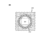
92 交差方向
100 伝熱管理装置
110 回路基板組立体
112 耐熱性の高い部品
114 耐熱性の低い部品
116 電気部品
118 ヒートシンク
120 プリント基板
122 電子部品取付モジュール
124 電子部品取付モジュール
130 目的とする伝熱領域
132 バルク領域
136 耐熱性の高い部品の設置領域
138 耐熱性の低い部品の設置領域
140 絶縁基板
142 導熱体
144 導電体
150 リング
152 スポーク
154 スポーク
230 目的とする伝熱領域
330 目的とする伝熱領域
400 伝熱管理装置
410 回路基板組立体
420 プリント基板
422 第1の積層
424 第2の積層
440 絶縁基板
442 導熱性
444 電子リード
500 伝熱管理装置
510 回路基板組立体
520 プリント基板
532 バルク領域
600 伝熱管理装置
602 電気モーター
604 固定子
606 回転子
610 除熱装置
620 プリント基板
630 目的とする伝熱領域
632 バルク領域
Claims (16)
- プリント基板であって、
絶縁基板と、
該絶縁基板に少なくとも部分的に組み込まれた導電体と、
前記絶縁基板に少なくとも部分的に組み込まれた導熱体であって、前記導電体から電気的に絶縁された導熱体と、
第1の設置領域と、
第2の設置領域と、を具備し、
前記絶縁基板及び前記導熱体が、
前記第2の設置領域近傍の伝熱領域であって、前記第2の設置領域を完全に包囲する前記導熱体の構成を有する伝熱領域、及び、
前記第2の設置領域から離れた位置におけるバルク領域であって、前記伝熱領域の導熱体と熱的導通状態にある前記導熱体の格子構成を有するバルク領域、
に構成された、プリント基板。 - 前記絶縁基板及び前記導熱体の前記バルク領域近傍に配置された電子部品取付モジュールを更に具備する請求項1に記載のプリント基板。
- 前記絶縁基板及び前記導熱体の前記伝熱領域近傍に配置された電子部品取付モジュールを更に具備する請求項1に記載のプリント基板。
- 前記絶縁基板及び前記導熱体の前記バルク領域近傍に配置されたヒートシンクを更に具備する請求項1に記載のプリント基板。
- 前記伝熱領域が、前記絶縁基板に組み込まれ且つ前記第2の設置領域を包囲する複数の導熱性リングを有する複合構造を更に具備する請求項1に記載のプリント基板。
- 前記伝熱領域が、前記絶縁基板に組み込まれ且つ前記第2の設置領域の周りで螺旋状の複数の導熱性スポークを有する複合構造を具備する請求項1に記載のプリント基板。
- 前記伝熱領域が、前記絶縁基板に組み込まれ且つ前記第2の設置領域の周りで径方向に配列された複数の導熱性スポークを有する複合構造を具備する請求項1に記載のプリント基板。
- 前記伝熱領域の有効熱伝導率が、前記バルク領域の有効熱伝導率の約10%の範囲内である請求項1に記載のプリント基板。
- 回路基板組立体であって、
絶縁基板、該絶縁基板に少なくとも部分的に組み込まれた導電体、該導電体と電気的導通状態にある第2の設置領域、前記導電体と電気的導通状態にある第1の設置領域、及び前記絶縁基板に少なくとも部分的に組み込まれた導熱体であって前記導電体から電気的に絶縁された導熱体、を有するプリント基板と、
前記第2の設置領域に結合された第2の部品と、
前記第1の設置領域に結合された第1の部品と、を具備し、
前記絶縁基板及び前記導熱体が、
前記第2の設置領域近傍の伝熱領域であって、前記第2の設置領域を完全に包囲する前記導熱体の構成を有する伝熱領域、及び、
前記第2の設置領域から離れた位置におけるバルク領域であって、前記伝熱領域の導熱体と熱的導通状態にある前記導熱体の格子構成を有するバルク領域、
に構成された、回路基板組立体。 - 前記導電体が、第1の積層板に組み込まれ、且つ、前記導熱体が、第2の積層板に組み込まれ、前記第1の積層板及び前記第2の積層板が、前記プリント基板において互いに結合された請求項9に記載の回路基板組立体。
- 前記導熱体が前記第2の設置領域近傍の伝熱領域に構成され、前記伝熱領域が、前記絶縁基板に組み込まれ且つ前記第2の設置領域を包囲する複数の導熱性リングを有する複合構造を具備する請求項9に記載の回路基板組立体。
- 前記導熱体が、前記第2の設置領域近傍の伝熱領域に構成され、前記伝熱領域が、前記絶縁基板に組み込まれ且つ前記第2の設置領域の周りで螺旋状の複数の導熱性スポークを有する複合構造を具備する請求項9に記載の回路基板組立体。
- 前記導熱体が前記第2の設置領域近傍の伝熱領域に構成され、前記伝熱領域が、前記絶縁基板に組み込まれ且つ前記第2の設置領域周りで径方向に配列された複数の導熱性スポークを有する複合構造を具備する請求項9に記載の回路基板組立体。
- 伝熱管理装置であって、
絶縁基板と、該絶縁基板に少なくとも部分的に組み込まれた導電体と、該絶縁基板に少なくとも部分的に組み込まれた導熱体であって前記導電体から電気的に絶縁された導熱体とを有するプリント基板と、
前記プリント基板に結合された第1の部品と、
前記プリント基板に結合され且つ前記第1の部品から遠位に配置された第2の部品と、を具備し、
前記プリント基板が、前記第1の部品及び前記第2の部品を互いに熱的導通状態に配置し、前記導熱体及び前記絶縁基板が、
前記第1の部品近傍の伝熱領域であって、前記第1の部品を完全に包囲する前記導熱体の構成を有する伝熱領域、及び、
前記第2の部品近傍のバルク領域であって、前記伝熱領域の導熱体と熱的導通状態にある前記導熱体の格子構成を有するバルク領域、
に構成された、伝熱管理装置。 - 前記伝熱領域の有効熱伝導率が、前記バルク領域の有効熱伝導率の約10%の範囲内である請求項14に記載の伝熱管理装置。
- 前記第1の部品が熱電発電器を具備する請求項14に記載の伝熱管理装置。
Applications Claiming Priority (4)
| Application Number | Priority Date | Filing Date | Title |
|---|---|---|---|
| US201361816917P | 2013-04-29 | 2013-04-29 | |
| US61/816,917 | 2013-04-29 | ||
| US14/038,834 | 2013-09-27 | ||
| US14/038,834 US9433074B2 (en) | 2013-04-29 | 2013-09-27 | Printed wiring boards having thermal management features and thermal management apparatuses comprising the same |
Publications (3)
| Publication Number | Publication Date |
|---|---|
| JP2014216656A JP2014216656A (ja) | 2014-11-17 |
| JP2014216656A5 JP2014216656A5 (ja) | 2016-08-25 |
| JP6306418B2 true JP6306418B2 (ja) | 2018-04-04 |
Family
ID=51788257
Family Applications (2)
| Application Number | Title | Priority Date | Filing Date |
|---|---|---|---|
| JP2014092593A Active JP6306418B2 (ja) | 2013-04-29 | 2014-04-28 | プリント基板、回路基板組立体及び伝熱管理装置 |
| JP2014092535A Pending JP2014216655A (ja) | 2013-04-29 | 2014-04-28 | 伝熱管理装置及び複合薄板 |
Family Applications After (1)
| Application Number | Title | Priority Date | Filing Date |
|---|---|---|---|
| JP2014092535A Pending JP2014216655A (ja) | 2013-04-29 | 2014-04-28 | 伝熱管理装置及び複合薄板 |
Country Status (2)
| Country | Link |
|---|---|
| US (2) | US9433074B2 (ja) |
| JP (2) | JP6306418B2 (ja) |
Families Citing this family (11)
| Publication number | Priority date | Publication date | Assignee | Title |
|---|---|---|---|---|
| US9511549B2 (en) * | 2014-06-02 | 2016-12-06 | Toyota Motor Engineering & Manufacturing North America, Inc. | Anisotropic thermal energy guiding shells and methods for fabricating thermal energy guiding shells |
| US9779199B2 (en) * | 2014-07-25 | 2017-10-03 | Toyota Motor Engineering & Manufacturing North America, Inc. | Circuit boards with thermal control and methods for their design |
| US9699883B2 (en) * | 2015-01-08 | 2017-07-04 | Toyota Motor Engineering & Manufacturing North America, Inc. | Thermal switches for active heat flux alteration |
| US10316852B2 (en) * | 2015-05-11 | 2019-06-11 | Hanon Systems | Air conditioner for vehicle |
| US10193047B2 (en) | 2015-08-14 | 2019-01-29 | Toyota Motor Engineering & Manufacturing North America, Inc. | Electronic assemblies incorporating heat flux routing structures for thermoelectric generation |
| US9990457B2 (en) | 2016-01-12 | 2018-06-05 | Toyota Motor Engineering & Manufacturing North America, Inc. | Switching circuit including wire traces to reduce the magnitude of voltage and current oscillations |
| US10206310B2 (en) | 2017-04-07 | 2019-02-12 | Toyota Motor Engineering & Manufacturing North America, Inc. | Electronics assemblies incorporating three-dimensional heat flow structures |
| JP2018192534A (ja) * | 2017-05-12 | 2018-12-06 | 国立大学法人 東京大学 | 熱流方向性制御構造 |
| US10627653B2 (en) | 2017-08-28 | 2020-04-21 | Toyota Motor Engineering & Manufacturing North America, Inc. | Thermal guiding for photonic components |
| US10962422B2 (en) | 2018-09-05 | 2021-03-30 | Hamilton Sundstrand Corporation | Differential and high rate of change temperature sensing circuit |
| CN112001080B (zh) * | 2020-08-25 | 2021-07-20 | 西南交通大学 | 一种轻量化车载牵引变压器绕组末端温度平均衰减量的计算方法 |
Family Cites Families (43)
| Publication number | Priority date | Publication date | Assignee | Title |
|---|---|---|---|---|
| US4853828A (en) * | 1985-08-22 | 1989-08-01 | Dart Controls, Inc. | Solid state device package mounting apparatus |
| US5123074A (en) * | 1988-02-26 | 1992-06-16 | Fujitsu Limited | Substrate for mounting optical components and electric circuit components thereon and method for making same |
| JPH04116146U (ja) * | 1991-03-25 | 1992-10-16 | ジエコー株式会社 | 回路基板構造 |
| DE69211074T2 (de) * | 1991-08-26 | 1996-10-02 | Sun Microsystems Inc | Verfahren und Apparat zum Kühlen von Mehrchip-Moduln durch die vollständige Wärmerohr-Technologie |
| JPH06209060A (ja) * | 1992-10-15 | 1994-07-26 | Sun Microsyst Inc | 半導体チップを冷却する装置及び方法 |
| US5419780A (en) * | 1994-04-29 | 1995-05-30 | Ast Research, Inc. | Method and apparatus for recovering power from semiconductor circuit using thermoelectric device |
| TW346566B (en) * | 1996-08-29 | 1998-12-01 | Showa Aluminiun Co Ltd | Radiator for portable electronic apparatus |
| JP3284969B2 (ja) * | 1998-05-11 | 2002-05-27 | 日本電気株式会社 | 多層配線基板 |
| US6257329B1 (en) * | 1998-08-17 | 2001-07-10 | Alfiero Balzano | Thermal management system |
| US6225571B1 (en) * | 1999-02-19 | 2001-05-01 | Lucent Technologies Inc. | Heatsink with high thermal conductivity dielectric |
| US6380633B1 (en) * | 2000-07-05 | 2002-04-30 | Siliconware Predision Industries Co., Ltd. | Pattern layout structure in substrate |
| JP3753995B2 (ja) * | 2002-03-13 | 2006-03-08 | インターナショナル・ビジネス・マシーンズ・コーポレーション | 冷却装置および情報処理装置 |
| US6657866B2 (en) * | 2002-03-15 | 2003-12-02 | Robert C. Morelock | Electronics assembly with improved heatsink configuration |
| DE10262012A1 (de) * | 2002-10-09 | 2004-04-22 | Infineon Technologies Ag | Speichermodul mit einer Wärmeableiteinrichtung |
| TW547918U (en) * | 2002-10-25 | 2003-08-11 | Hon Hai Prec Ind Co Ltd | Heat dissipating device |
| US7308008B2 (en) | 2002-11-08 | 2007-12-11 | Finisar Corporation | Magnetically controlled heat sink |
| JP4325263B2 (ja) * | 2003-04-21 | 2009-09-02 | ソニー株式会社 | 回路装置及び電子機器 |
| US6901994B1 (en) * | 2004-01-05 | 2005-06-07 | Industrial Technology Research Institute | Flat heat pipe provided with means to enhance heat transfer thereof |
| US6957692B1 (en) * | 2004-08-31 | 2005-10-25 | Inventec Corporation | Heat-dissipating device |
| TWI273210B (en) * | 2004-12-30 | 2007-02-11 | Delta Electronics Inc | Heat-dissipation device and fabricating method thereof |
| TWI309549B (en) * | 2005-08-29 | 2009-05-01 | Via Tech Inc | Printed circuit board with improved thermal dissipating structure and electronic device with the same |
| US20070108595A1 (en) | 2005-11-16 | 2007-05-17 | Ati Technologies Inc. | Semiconductor device with integrated heat spreader |
| JP2008060430A (ja) * | 2006-08-31 | 2008-03-13 | Daikin Ind Ltd | 電力変換装置 |
| JP4277036B2 (ja) * | 2006-09-29 | 2009-06-10 | Tdk株式会社 | 半導体内蔵基板及びその製造方法 |
| TW200928203A (en) * | 2007-12-24 | 2009-07-01 | Guei-Fang Chen | LED illuminating device capable of quickly dissipating heat and its manufacturing method |
| US7942196B2 (en) * | 2007-12-27 | 2011-05-17 | Fu Zhun Precision Industry (Shen Zhen) Co., Ltd. | Heat spreader with vapor chamber |
| JP2009164273A (ja) * | 2007-12-28 | 2009-07-23 | Hitachi Ltd | 回路基板 |
| US7800904B2 (en) * | 2008-01-15 | 2010-09-21 | Mcgough William L | Electronic assembly and heat sink |
| US8110446B2 (en) * | 2008-03-25 | 2012-02-07 | Bridge Semiconductor Corporation | Method of making a semiconductor chip assembly with a post/base heat spreader and a conductive trace |
| US7952114B2 (en) * | 2008-09-23 | 2011-05-31 | Tyco Electronics Corporation | LED interconnect assembly |
| JP2010165728A (ja) * | 2009-01-13 | 2010-07-29 | Kyocera Corp | 多層基板及び携帯通信機器 |
| US20100188848A1 (en) * | 2009-01-28 | 2010-07-29 | Been-Yu Liaw | Electro-thermal separation light emitting diode light engine module |
| TWI377465B (en) | 2010-03-11 | 2012-11-21 | Delta Electronics Inc | Heat dissipating module and electronic device using such heat dissipating module |
| US20110272179A1 (en) * | 2010-05-06 | 2011-11-10 | Vasoya Kalu K | Printed Circuit Board with Embossed Hollow Heatsink Pad |
| US8391009B2 (en) * | 2010-06-18 | 2013-03-05 | Sunonwealth Electric Machine Industry Co., Ltd. | Heat dissipating assembly |
| CN102548341A (zh) | 2010-12-10 | 2012-07-04 | 旭丽电子(广州)有限公司 | 散热壳体结构 |
| CN102026496A (zh) * | 2010-12-24 | 2011-04-20 | 乐健线路板(珠海)有限公司 | 带有绝缘微散热器的印刷电路板的制备方法 |
| US8649179B2 (en) * | 2011-02-05 | 2014-02-11 | Laird Technologies, Inc. | Circuit assemblies including thermoelectric modules |
| KR20130027611A (ko) * | 2011-05-18 | 2013-03-18 | 삼성전자주식회사 | Led 모듈 및 이를 포함하는 백라이트 유닛, led 모듈의 제조방법 |
| US8976527B2 (en) * | 2012-09-29 | 2015-03-10 | Apple Inc. | Force and heat spreading PCB for LCD protection and interconnection |
| US9125299B2 (en) * | 2012-12-06 | 2015-09-01 | Apple Inc. | Cooling for electronic components |
| US9282596B2 (en) * | 2012-12-13 | 2016-03-08 | Power Gold LLC | Intelligent lighting system |
| CN104112724A (zh) * | 2013-04-22 | 2014-10-22 | 华硕电脑股份有限公司 | 散热元件 |
-
2013
- 2013-09-27 US US14/038,834 patent/US9433074B2/en active Active
- 2013-09-27 US US14/038,837 patent/US20140318758A1/en not_active Abandoned
-
2014
- 2014-04-28 JP JP2014092593A patent/JP6306418B2/ja active Active
- 2014-04-28 JP JP2014092535A patent/JP2014216655A/ja active Pending
Also Published As
| Publication number | Publication date |
|---|---|
| US20140318758A1 (en) | 2014-10-30 |
| US20140318829A1 (en) | 2014-10-30 |
| JP2014216656A (ja) | 2014-11-17 |
| US9433074B2 (en) | 2016-08-30 |
| JP2014216655A (ja) | 2014-11-17 |
Similar Documents
| Publication | Publication Date | Title |
|---|---|---|
| JP6306418B2 (ja) | プリント基板、回路基板組立体及び伝熱管理装置 | |
| JP5769823B2 (ja) | 熱電モジュールを含む回路アセンブリ | |
| CN104282679B (zh) | 带有功率半导体的电子组件 | |
| JP7171725B2 (ja) | 熱変換装置 | |
| JP6119602B2 (ja) | 電子装置 | |
| US8730674B2 (en) | Magnetic fluid cooling devices and power electronics assemblies | |
| KR102434261B1 (ko) | 열변환장치 | |
| JP6426548B2 (ja) | 温度制御を有する回路基板及びその設計方法 | |
| JP2022522413A (ja) | 相互接続 | |
| JP5963732B2 (ja) | チップ支持基板の配線部裏面に放熱器設置の面領域を設定する方法およびチップ支持基板並びにチップ実装構造体 | |
| JP6856730B2 (ja) | 複合層を有する熱伝達管理装置 | |
| US10367498B2 (en) | Thermally controlled electronic device | |
| JP7072004B2 (ja) | 熱変換装置 | |
| CN104125707B (zh) | 印刷线路板、电路板组装件、热传递管理装置 | |
| Cairnie et al. | Thermal and thermomechanical analysis of a 10 kV SiC MOSFET package with double-sided cooling | |
| WO2020100749A1 (ja) | 熱電変換モジュール | |
| CN109156081A (zh) | 电子模块及电子模块的制造方法 | |
| RU2589744C2 (ru) | Устройство термостабилизации и отвода тепла от электронных модулей радиотелевизионной аппаратуры | |
| Jaziri et al. | A novel 2-in-1 heat management and recovery system for sustainable electronics | |
| JP3100714U (ja) | 熱放散板モジュール | |
| CN104125755A (zh) | 具有热管理特征的复合层及包括该复合层的热管理装置 | |
| CN109089374A (zh) | 一种pcb电路板局部散热方法 | |
| TWM329810U (en) | Heat dissipation device | |
| CN107333386A (zh) | Pcb板的散热结构及方法 | |
| KR20170139356A (ko) | 충전 장치 |
Legal Events
| Date | Code | Title | Description |
|---|---|---|---|
| A521 | Request for written amendment filed |
Free format text: JAPANESE INTERMEDIATE CODE: A523 Effective date: 20160711 |
|
| A621 | Written request for application examination |
Free format text: JAPANESE INTERMEDIATE CODE: A621 Effective date: 20160711 |
|
| A977 | Report on retrieval |
Free format text: JAPANESE INTERMEDIATE CODE: A971007 Effective date: 20170427 |
|
| A131 | Notification of reasons for refusal |
Free format text: JAPANESE INTERMEDIATE CODE: A131 Effective date: 20170530 |
|
| A521 | Request for written amendment filed |
Free format text: JAPANESE INTERMEDIATE CODE: A523 Effective date: 20170822 |
|
| TRDD | Decision of grant or rejection written | ||
| A01 | Written decision to grant a patent or to grant a registration (utility model) |
Free format text: JAPANESE INTERMEDIATE CODE: A01 Effective date: 20180206 |
|
| A61 | First payment of annual fees (during grant procedure) |
Free format text: JAPANESE INTERMEDIATE CODE: A61 Effective date: 20180308 |
|
| R150 | Certificate of patent or registration of utility model |
Ref document number: 6306418 Country of ref document: JP Free format text: JAPANESE INTERMEDIATE CODE: R150 |
|
| S111 | Request for change of ownership or part of ownership |
Free format text: JAPANESE INTERMEDIATE CODE: R313113 |
|
| R350 | Written notification of registration of transfer |
Free format text: JAPANESE INTERMEDIATE CODE: R350 |