JP6288879B2 - 高周波半導体モジュール - Google Patents
高周波半導体モジュール Download PDFInfo
- Publication number
- JP6288879B2 JP6288879B2 JP2016172849A JP2016172849A JP6288879B2 JP 6288879 B2 JP6288879 B2 JP 6288879B2 JP 2016172849 A JP2016172849 A JP 2016172849A JP 2016172849 A JP2016172849 A JP 2016172849A JP 6288879 B2 JP6288879 B2 JP 6288879B2
- Authority
- JP
- Japan
- Prior art keywords
- heat sink
- output voltage
- frequency semiconductor
- ground
- semiconductor module
- Prior art date
- Legal status (The legal status is an assumption and is not a legal conclusion. Google has not performed a legal analysis and makes no representation as to the accuracy of the status listed.)
- Active
Links
Images


Classifications
-
- H—ELECTRICITY
- H01—ELECTRIC ELEMENTS
- H01L—SEMICONDUCTOR DEVICES NOT COVERED BY CLASS H10
- H01L2224/00—Indexing scheme for arrangements for connecting or disconnecting semiconductor or solid-state bodies and methods related thereto as covered by H01L24/00
- H01L2224/01—Means for bonding being attached to, or being formed on, the surface to be connected, e.g. chip-to-package, die-attach, "first-level" interconnects; Manufacturing methods related thereto
- H01L2224/42—Wire connectors; Manufacturing methods related thereto
- H01L2224/47—Structure, shape, material or disposition of the wire connectors after the connecting process
- H01L2224/48—Structure, shape, material or disposition of the wire connectors after the connecting process of an individual wire connector
- H01L2224/4805—Shape
- H01L2224/4809—Loop shape
- H01L2224/48091—Arched
-
- H—ELECTRICITY
- H01—ELECTRIC ELEMENTS
- H01L—SEMICONDUCTOR DEVICES NOT COVERED BY CLASS H10
- H01L2224/00—Indexing scheme for arrangements for connecting or disconnecting semiconductor or solid-state bodies and methods related thereto as covered by H01L24/00
- H01L2224/01—Means for bonding being attached to, or being formed on, the surface to be connected, e.g. chip-to-package, die-attach, "first-level" interconnects; Manufacturing methods related thereto
- H01L2224/42—Wire connectors; Manufacturing methods related thereto
- H01L2224/47—Structure, shape, material or disposition of the wire connectors after the connecting process
- H01L2224/49—Structure, shape, material or disposition of the wire connectors after the connecting process of a plurality of wire connectors
- H01L2224/491—Disposition
- H01L2224/4912—Layout
- H01L2224/49175—Parallel arrangements
Landscapes
- Cooling Or The Like Of Semiconductors Or Solid State Devices (AREA)
Description
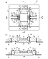
本実施形態における高周波半導体モジュール10について、図3を参照して説明する。図3は、本実施形態における高周波半導体モジュール10の構成例を説明するための図であって、(a)は高周波半導体モジュール10の上面図、(b)はA−A´断面図、(c)はB−B´断面図を示す。
できる。この場合も、キャビティ40のサイズをICチップ31のサイズよりも0.5mm程度大きくし、ワイヤの長さが1mm未満になるようにして、バイパス効果が低下しないようにする。
各グランドリード53は、グランドリード固定部53aにおいて、パッケージに固定され、パッケージのグランドと電気的に接続される。
S=N*π(r2−(r−h)2) =0.89 [mm2] (1)
A = T/(σ・S) =5.6 [K/W] (2)
上述した高周波半導体モジュール10の10 K/Wとの熱抵抗として加えると、15.6 K/W程度となる。これは、上記の条件を満たすことがわかる。
11 積層セラミック基板
12a,12b,12c グランドパッド
15a,15b 信号配線
17 ビア
20 ヒートシンク
32 コンデンサ
40 キャビティ
53 グランドリード
61 放熱ビア
151a,151b 信号用リード
Claims (4)
- 高周波半導体モジュールであって、
キャビティを有する誘電体基板と、
前記キャビティ内の下部に設けられたヒートシンクと、
前記ヒートシンク上に設けられ、信号用リードと信号配線を介して接続される半導体チップと、
前記ヒートシンク上に設けられたコンデンサと、
前記誘電体基板上面に設けられ、前記コンデンサとボンディングワイヤを介して接続される直流端子と、
前記誘電体基板下面に設けられた直流用リードと、
を備え、
前記半導体チップの実装面と前記コンデンサの実装面とは、前記キャビティ内にある前記ヒートシンクの上面側に位置し、
前記誘電体基板の底面に形成されるグランドは、前記誘電体基板の底面に形成されたグランドリードと電気的に接続されており、
前記直流端子と前記直流用リードが、前記誘電体基板内部に形成されたビアを介して電気的に接続され、
前記信号配線が2本の差動信号用線路として形成されている場合において、前記信号配線の入力側では、入力側の2本の信号配線の入力のうち片側の入力電圧増加に対して出力電圧が増加する場合は他方の入力電圧に対して出力電圧が減少し、逆に片側の入力電圧に対して出力電圧が減少する場合は前記増加する動作の場合とは逆の動作を行い、かつ、
前記信号配線の出力側では、出力側の2本の信号配線の出力のうち片側の出力電圧が増加する場合は他方の出力電圧が減少し、逆に片側の出力電圧が減少する場合は常に他方の出力電圧が増加するという相補的な動作をし、前記2本の差動信号用線路の間は、グランド用ボンディング、グランド用ビア、および、グランド用パッドを有しない
ことを特徴とする高周波半導体モジュール。 - 前記ヒートシンクは、当該ヒートシンクの底面が前記高周波半導体モジュールの底面から突出しないように形成されていることを特徴とする請求項1に記載の高周波半導体モジュール。
- 前記信号配線は、ビア導体または表面配線を含むことを特徴とする請求項1または2に記載の高周波半導体モジュール。
- 前記コンデンサは、バイパス用のチップコンデンサであることを特徴とする請求項1ないし3のいずれか1項に記載の高周波半導体モジュール。
Priority Applications (1)
| Application Number | Priority Date | Filing Date | Title |
|---|---|---|---|
| JP2016172849A JP6288879B2 (ja) | 2016-09-05 | 2016-09-05 | 高周波半導体モジュール |
Applications Claiming Priority (1)
| Application Number | Priority Date | Filing Date | Title |
|---|---|---|---|
| JP2016172849A JP6288879B2 (ja) | 2016-09-05 | 2016-09-05 | 高周波半導体モジュール |
Related Parent Applications (1)
| Application Number | Title | Priority Date | Filing Date |
|---|---|---|---|
| JP2013043515A Division JP2014175319A (ja) | 2013-03-05 | 2013-03-05 | 高周波半導体モジュール |
Publications (2)
| Publication Number | Publication Date |
|---|---|
| JP2016201576A JP2016201576A (ja) | 2016-12-01 |
| JP6288879B2 true JP6288879B2 (ja) | 2018-03-07 |
Family
ID=57422844
Family Applications (1)
| Application Number | Title | Priority Date | Filing Date |
|---|---|---|---|
| JP2016172849A Active JP6288879B2 (ja) | 2016-09-05 | 2016-09-05 | 高周波半導体モジュール |
Country Status (1)
| Country | Link |
|---|---|
| JP (1) | JP6288879B2 (ja) |
Cited By (1)
| Publication number | Priority date | Publication date | Assignee | Title |
|---|---|---|---|---|
| WO2019182197A1 (ko) * | 2018-03-23 | 2019-09-26 | 김선국 | 알에프 칩 패키지 |
Family Cites Families (9)
| Publication number | Priority date | Publication date | Assignee | Title |
|---|---|---|---|---|
| JPS63174342A (ja) * | 1987-01-14 | 1988-07-18 | Toshiba Corp | 高周波半導体用外囲器 |
| JPH03270054A (ja) * | 1990-03-19 | 1991-12-02 | Nec Corp | 高周波高出力半導体装置 |
| US6127894A (en) * | 1998-01-21 | 2000-10-03 | Uniden San Diego Research & Development Center, Inc. | High frequency shunt feedback amplifier topology |
| JPH11251488A (ja) * | 1998-03-05 | 1999-09-17 | Sumitomo Metal Electronics Devices Inc | セラミックパッケージ |
| JP2002184900A (ja) * | 2000-12-19 | 2002-06-28 | Mitsubishi Electric Corp | 多層高周波パッケージ基板 |
| JP2004179198A (ja) * | 2002-11-25 | 2004-06-24 | Shinko Electric Ind Co Ltd | セラミックパッケージ |
| JP2004311795A (ja) * | 2003-04-09 | 2004-11-04 | Sumitomo Metal Electronics Devices Inc | 半導体素子収納用パッケージ |
| JP2004356352A (ja) * | 2003-05-28 | 2004-12-16 | Kyocera Corp | 高周波回路用パッケージ |
| JP2011238687A (ja) * | 2010-05-07 | 2011-11-24 | Sumitomo Electric Ind Ltd | 回路装置及び半導体装置 |
-
2016
- 2016-09-05 JP JP2016172849A patent/JP6288879B2/ja active Active
Cited By (1)
| Publication number | Priority date | Publication date | Assignee | Title |
|---|---|---|---|---|
| WO2019182197A1 (ko) * | 2018-03-23 | 2019-09-26 | 김선국 | 알에프 칩 패키지 |
Also Published As
| Publication number | Publication date |
|---|---|
| JP2016201576A (ja) | 2016-12-01 |
Similar Documents
| Publication | Publication Date | Title |
|---|---|---|
| JP3803596B2 (ja) | パッケージ型半導体装置 | |
| JP5180176B2 (ja) | To−can型tosaモジュール | |
| JP5144628B2 (ja) | To−can型tosaモジュール | |
| JP7095583B2 (ja) | 光送信機 | |
| JP4159778B2 (ja) | Icパッケージ、光送信器及び光受信器 | |
| JP2011108937A (ja) | To−can型tosaモジュール | |
| JP6183479B2 (ja) | 光変調器及びそれを用いた光送信装置 | |
| CN111868589B (zh) | 激光器、激光器阵列的封装结构及封装组件 | |
| JP5241562B2 (ja) | 接続装置、フレキシブル基板付き半導体素子収納用パッケージ、およびフレキシブル基板付き半導体装置 | |
| JP2011108940A (ja) | To−can型tosaモジュール用実装構成およびto−can型tosaモジュール | |
| JP6288879B2 (ja) | 高周波半導体モジュール | |
| JP2014175319A (ja) | 高周波半導体モジュール | |
| JP2017058607A (ja) | 光伝送装置及び光モジュール | |
| JP2004093606A (ja) | 光モジュール及び光伝送装置 | |
| JP5112962B2 (ja) | パッケージ | |
| JP2019046883A (ja) | 半導体装置およびその製造方法 | |
| JP2001308235A (ja) | 半導体モジュール | |
| JPH04349686A (ja) | チップキャリア | |
| JP3555304B2 (ja) | 電子装置 | |
| US20230244045A1 (en) | OPTO-Electronic Integrated Module | |
| JP2015065255A (ja) | 光電融合モジュール | |
| WO2024013827A1 (ja) | 高速光送受信装置 | |
| JP7246590B1 (ja) | 半導体レーザ光源装置 | |
| US20230116287A1 (en) | Optical module | |
| JP7074012B2 (ja) | 光モジュール |
Legal Events
| Date | Code | Title | Description |
|---|---|---|---|
| A621 | Written request for application examination |
Free format text: JAPANESE INTERMEDIATE CODE: A621 Effective date: 20160905 |
|
| A977 | Report on retrieval |
Free format text: JAPANESE INTERMEDIATE CODE: A971007 Effective date: 20170619 |
|
| A131 | Notification of reasons for refusal |
Free format text: JAPANESE INTERMEDIATE CODE: A131 Effective date: 20170705 |
|
| A521 | Request for written amendment filed |
Free format text: JAPANESE INTERMEDIATE CODE: A523 Effective date: 20170830 |
|
| TRDD | Decision of grant or rejection written | ||
| A01 | Written decision to grant a patent or to grant a registration (utility model) |
Free format text: JAPANESE INTERMEDIATE CODE: A01 Effective date: 20180131 |
|
| A61 | First payment of annual fees (during grant procedure) |
Free format text: JAPANESE INTERMEDIATE CODE: A61 Effective date: 20180205 |
|
| R150 | Certificate of patent or registration of utility model |
Ref document number: 6288879 Country of ref document: JP Free format text: JAPANESE INTERMEDIATE CODE: R150 |