JP6140923B2 - スポットサイズ変換器、光送信器、光受信器、光送受信器及びスポットサイズ変換器の製造方法 - Google Patents
スポットサイズ変換器、光送信器、光受信器、光送受信器及びスポットサイズ変換器の製造方法 Download PDFInfo
- Publication number
- JP6140923B2 JP6140923B2 JP2011289548A JP2011289548A JP6140923B2 JP 6140923 B2 JP6140923 B2 JP 6140923B2 JP 2011289548 A JP2011289548 A JP 2011289548A JP 2011289548 A JP2011289548 A JP 2011289548A JP 6140923 B2 JP6140923 B2 JP 6140923B2
- Authority
- JP
- Japan
- Prior art keywords
- core layer
- layer
- cross
- light
- spot size
- Prior art date
- Legal status (The legal status is an assumption and is not a legal conclusion. Google has not performed a legal analysis and makes no representation as to the accuracy of the status listed.)
- Active
Links
Images


Classifications
-
- G—PHYSICS
- G02—OPTICS
- G02B—OPTICAL ELEMENTS, SYSTEMS OR APPARATUS
- G02B6/00—Light guides; Structural details of arrangements comprising light guides and other optical elements, e.g. couplings
- G02B6/02—Optical fibres with cladding with or without a coating
- G02B6/036—Optical fibres with cladding with or without a coating core or cladding comprising multiple layers
-
- G—PHYSICS
- G02—OPTICS
- G02B—OPTICAL ELEMENTS, SYSTEMS OR APPARATUS
- G02B6/00—Light guides; Structural details of arrangements comprising light guides and other optical elements, e.g. couplings
- G02B6/10—Light guides; Structural details of arrangements comprising light guides and other optical elements, e.g. couplings of the optical waveguide type
- G02B6/12—Light guides; Structural details of arrangements comprising light guides and other optical elements, e.g. couplings of the optical waveguide type of the integrated circuit kind
- G02B6/122—Basic optical elements, e.g. light-guiding paths
- G02B6/1228—Tapered waveguides, e.g. integrated spot-size transformers
-
- G—PHYSICS
- G02—OPTICS
- G02B—OPTICAL ELEMENTS, SYSTEMS OR APPARATUS
- G02B6/00—Light guides; Structural details of arrangements comprising light guides and other optical elements, e.g. couplings
- G02B6/24—Coupling light guides
- G02B6/26—Optical coupling means
- G02B6/30—Optical coupling means for use between fibre and thin-film device
- G02B6/305—Optical coupling means for use between fibre and thin-film device and having an integrated mode-size expanding section, e.g. tapered waveguide
-
- G—PHYSICS
- G02—OPTICS
- G02B—OPTICAL ELEMENTS, SYSTEMS OR APPARATUS
- G02B6/00—Light guides; Structural details of arrangements comprising light guides and other optical elements, e.g. couplings
- G02B6/10—Light guides; Structural details of arrangements comprising light guides and other optical elements, e.g. couplings of the optical waveguide type
- G02B6/12—Light guides; Structural details of arrangements comprising light guides and other optical elements, e.g. couplings of the optical waveguide type of the integrated circuit kind
- G02B2006/12083—Constructional arrangements
- G02B2006/12097—Ridge, rib or the like
-
- G—PHYSICS
- G02—OPTICS
- G02B—OPTICAL ELEMENTS, SYSTEMS OR APPARATUS
- G02B6/00—Light guides; Structural details of arrangements comprising light guides and other optical elements, e.g. couplings
- G02B6/10—Light guides; Structural details of arrangements comprising light guides and other optical elements, e.g. couplings of the optical waveguide type
- G02B6/12—Light guides; Structural details of arrangements comprising light guides and other optical elements, e.g. couplings of the optical waveguide type of the integrated circuit kind
- G02B2006/12166—Manufacturing methods
- G02B2006/12195—Tapering
-
- G—PHYSICS
- G02—OPTICS
- G02B—OPTICAL ELEMENTS, SYSTEMS OR APPARATUS
- G02B6/00—Light guides; Structural details of arrangements comprising light guides and other optical elements, e.g. couplings
- G02B6/10—Light guides; Structural details of arrangements comprising light guides and other optical elements, e.g. couplings of the optical waveguide type
- G02B6/12—Light guides; Structural details of arrangements comprising light guides and other optical elements, e.g. couplings of the optical waveguide type of the integrated circuit kind
- G02B6/13—Integrated optical circuits characterised by the manufacturing method
- G02B6/136—Integrated optical circuits characterised by the manufacturing method by etching
-
- G—PHYSICS
- G02—OPTICS
- G02B—OPTICAL ELEMENTS, SYSTEMS OR APPARATUS
- G02B6/00—Light guides; Structural details of arrangements comprising light guides and other optical elements, e.g. couplings
- G02B6/24—Coupling light guides
- G02B6/26—Optical coupling means
- G02B6/30—Optical coupling means for use between fibre and thin-film device
Landscapes
- Physics & Mathematics (AREA)
- General Physics & Mathematics (AREA)
- Optics & Photonics (AREA)
- Engineering & Computer Science (AREA)
- Power Engineering (AREA)
- Microelectronics & Electronic Packaging (AREA)
- Optical Integrated Circuits (AREA)
- Optical Couplings Of Light Guides (AREA)
- Semiconductor Lasers (AREA)
Description
第1クラッド層と、
光を入出力する第1端部から第2端部に向かう方向に沿って前記第1端部から延びるように、前記第1クラッド層上に並んで配置された第1コア層及び第2コア層と、
前記第1コア層と前記第2コア層との間で前記第1クラッド層上に配置され、前記第1コア層及び前記第2コア層とは別体であり、前記第1端部から前記第2端部に向かう方向に沿って前記第2端部まで延びる第3コア層と、
前記第1コア層及び前記第2コア層及び前記第3コア層上に配置された第2クラッド層と、
を備えるスポットサイズ変換器。
前記第3コア層は、前記第1コア層と前記第2コア層との間の中央に配置される付記1に記載のスポットサイズ変換器。
前記第3コア層は、前記第1端部から前記第2端部に向かう方向において、断面積が増加する付記1又は2に記載のスポットサイズ変換器。
前記第3コア層は、前記第1端部から前記第2端部に向かう方向において、前記第1コア層及び前記第2コア層の断面積が最小値を示す位置で、前記第3コア層の断面積が最大となる付記3に記載のスポットサイズ変換器。
前記第3コア層は、前記第1端部から前記第2端部に向かう方向において、前記第1コア層及び前記第2コア層の断面積が最大となる位置から前記第2端部まで延びるように配置される付記3又は4に記載のスポットサイズ変換器。
前記第1コア層及び前記第2コア層は、前記第1端部から前記第2端部に向かう方向において、断面積が一定であるか又は減少する付記1〜4の何れか一項に記載のスポットサイズ変換器。
前記第1コア層及び前記第2コア層は、両コア層の間の中心線に対して線対称の関係にある付記1〜6の何れか一項に記載のスポットサイズ変換器。
前記第1コア層及び前記第2コア層及び前記第3コア層の厚さは一定である付記1〜7の何れか一項に記載のスポットサイズ変換器。
前記第1端部から、前記第1クラッド層及び前記第2クラッド層が延出しており、前記第1クラッド層と前記第2クラッド層とが積層された延出部が形成される付記1〜8の何れか一項に記載のスポットサイズ変換器。
基板と、
前記基板上に配置された第1クラッド層と、
光を入力する第1端部から第2端部に向かう方向に沿って前記第1端部から延びるように、前記第1クラッド層上に並んで配置された第1コア層及び第2コア層と、
前記第1コア層と前記第2コア層との間で前記第1クラッド層上に配置され、前記第1コア層及び前記第2コア層とは別体であり、前記第1端部から前記第2端部に向かう方向に沿って前記第2端部まで延びる第3コア層と、
前記第1コア層及び前記第2コア層及び前記第3コア層上に配置された第2クラッド層と、を有するスポットサイズ変換部と、
前記基板上に配置され、前記第1端部に光を出力する光発生部と、
を備える光送信器。
基板と、
前記基板上に配置された第1クラッド層と、
光を入力する第1端部から第2端部に向かう方向に沿って前記第1端部から延びるように、前記第1クラッド層上に並んで配置された第1コア層及び第2コア層と、
前記第1コア層と前記第2コア層との間で前記第1クラッド層上に配置され、前記第1コア層及び前記第2コア層とは別体であり、前記第1端部から前記第2端部に向かう方向に沿って前記第2端部まで延びる第3コア層と、
前記第1コア層及び前記第2コア層及び前記第3コア層上に配置された第2クラッド層と、を有するスポットサイズ変換部と、
前記基板上に配置され、前記第2端部から入力され前記スポットサイズ変換器を伝搬して前記第1端部から出力された光を検出する光検出部と、
を備える光受信器。
第1基板と、
前記第1基板上に配置された第1クラッド層と、
光を入力する第1端部から光を出力する第2端部に向かう方向に沿って前記第1端部から延びるように、前記第1クラッド層上に並んで配置された第1コア層及び第2コア層と、
前記第1コア層と前記第2コア層との間で前記第1クラッド層上に配置され、前記第1コア層及び前記第2コア層とは別体であり、前記第1端部から前記第2端部に向かう方向に沿って前記第2端部まで延びる第3コア層と、
前記第1コア層及び前記第2コア層及び前記第3コア層上に配置された第2クラッド層と、を有する第1のスポットサイズ変換部と、
前記第1基板上に配置され、前記第1端部に光を出力する光発生部と、
第2基板と、
前記第2基板上に配置された第3クラッド層と、
光を出力する第3端部から光を入力する第4端部に向かう方向に沿って前記第3端部から延びるように、前記第3クラッド層上に並んで配置された第4コア層及び第5コア層と、
前記第4コア層と前記第5コア層との間で前記第3クラッド層上に配置され、前記第4コア層及び前記第5コア層とは別体であり、前記第3端部から前記第4端部に向かう方向に沿って前記第4端部まで延びる第6コア層と、
前記第4コア層及び前記第5コア層及び前記第6コア層上に配置された前記第4クラッド層と、を有する第2のスポットサイズ変換部と、
前記第2基板上に配置され、前記第4端部から入力され前記第2のスポットサイズ変換器を伝搬して前記第3端部から出力された光を検出する光検出部と、
を備える光送受信器。
第1クラッド層上に、第1端部から第2端部に向かう方向に沿って前記第1端部から延びるように、前記第1クラッド層上に並んで配置された第1コア層及び第2コア層を形成すると共に、前記第1コア層と前記第2コア層との間の前記第1クラッド層上に、前記第1コア層及び前記第2コア層とは別体であり、前記第1端部から前記第2端部に向かう方向に沿って前記第2端部まで延びる第3コア層を形成し、
前記第1コア層及び前記第2コア層及び前記第3コア層上に第2クラッド層を形成するスポットサイズ変換器の製造方法。
10a 第1延出部
10b スポットサイズ変換部
10c 第2延出部
11 基板
12 下クラッド層 (第1クラッド層)
13 第1コア層
13a 第1コア延出部
14 第2コア層
14a 第2コア延出部
15 第3コア層
15a 第3コア延出部
16 上クラッド層 (第2クラッド層)
20 伝搬するフィールドのモードプロファイル
21 伝搬するフィールドのモードプロファイル
22 伝搬するフィールドのモードプロファイル
30 光素子
30a 第1延出部
30b スポットサイズ変換部
30c 第2延出部
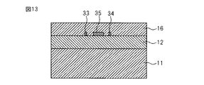
33 第1コア層
33a 第1延出部
34 第2コア層
34a 第2延出部
35 第3コア層
40 光送信器
41 光素子
41a スポットサイズ変換部
42 光発生部
50 光送信器
51a、51b、51c 光素子
52a、52b、52c 光発生部
60 光送受信器
61 第1光素子
61a スポットサイズ変換部
62 光発生部
63 光変調部
64 出力部
65 光検出部
66 第2光素子
66a スポットサイズ変換部
67 入力部
70、71、72 マスク
80 スポットサイズ変換器
83 第1コア層
84 第2コア層
85 第3コア層
Claims (5)
- 第1クラッド層と、
光を入出力する第1端部から第2端部に向かう方向に沿って前記第1端部から延びるように、前記第1クラッド層上に並んで配置された第1コア層及び第2コア層と、
前記第1コア層と前記第2コア層との間で前記第1クラッド層上に配置され、前記第1コア層及び前記第2コア層とは別体であり、前記第1端部から前記第2端部に向かう方向に沿って前記第2端部まで延びる第3コア層と、
前記第1コア層及び前記第2コア層及び前記第3コア層上に配置された第2クラッド層と、
を備え、
前記第1コア層及び前記第2コア層の断面積は、前記第1端部から前記第2端部に向かう方向において増加して最大となった後減少しており、
前記第3コア層は、前記第1端部から前記第2端部に向かう方向において、前記第1コア層及び前記第2コア層の断面積が最大となる位置から前記第2端部まで断面積が増加しながら延びるように配置され、且つ、前記第1端部から前記第2端部に向かう方向において、前記第1コア層及び前記第2コア層の断面積が最小値を示す位置で、前記第3コア層の断面積が最大となる、スポットサイズ変換器。 - 基板と、
前記基板上に配置された第1クラッド層と、
光を入力する第1端部から光を出力する第2端部に向かう方向に沿って前記第1端部から延びるように、前記第1クラッド層上に並んで配置された第1コア層及び第2コア層と、
前記第1コア層と前記第2コア層との間で前記第1クラッド層上に配置され、前記第1コア層及び前記第2コア層とは別体であり、前記第1端部から前記第2端部に向かう方向に沿って前記第2端部まで延びる第3コア層と、
前記第1コア層及び前記第2コア層及び前記第3コア層上に配置された第2クラッド層と、を有し、
前記第1コア層及び前記第2コア層の断面積は、前記第1端部から前記第2端部に向かう方向において、増加して最大となった後減少しており、
前記第3コア層は、前記第1端部から前記第2端部に向かう方向において、前記第1コア層及び前記第2コア層の断面積が最大となる位置から前記第2端部まで断面積が増加しながら延びるように配置され、且つ、前記第1端部から前記第2端部に向かう方向において、前記第1コア層及び前記第2コア層の断面積が最小値を示す位置で、前記第3コア層の断面積が最大となる、スポットサイズ変換部と、
前記基板上に配置され、前記第1端部に入力され前記スポットサイズ変換部を伝搬して前記第2端部から出力される光を発生する光発生部と、
を備える光送信器。 - 基板と、
前記基板上に配置された第1クラッド層と、
光を出力する第1端部から光を入力する第2端部に向かう方向に沿って前記第1端部から延びるように、前記第1クラッド層上に並んで配置された第1コア層及び第2コア層と、
前記第1コア層と前記第2コア層との間で前記第1クラッド層上に配置され、前記第1コア層及び前記第2コア層とは別体であり、前記第1端部から前記第2端部に向かう方向に沿って前記第2端部まで延びる第3コア層と、
前記第1コア層及び前記第2コア層及び前記第3コア層上に配置された第2クラッド層と、を有し、
前記第1コア層及び前記第2コア層の断面積は、前記第1端部から前記第2端部に向かう方向において増加して最大となった後減少しており、
前記第3コア層は、前記第1端部から前記第2端部に向かう方向において、前記第1コア層及び前記第2コア層の断面積が最大となる位置から前記第2端部まで断面積が増加しながら延びるように配置され、且つ、前記第1端部から前記第2端部に向かう方向において、前記第1コア層及び前記第2コア層の断面積が最小値を示す位置で、前記第3コア層の断面積が最大となる、スポットサイズ変換部と、
前記基板上に配置され、前記第2端部から入力され前記スポットサイズ変換器を伝搬して前記第1端部から出力された光を検出する光検出部と、
を備える光受信器。 - 第1基板と、
前記第1基板上に配置された第1クラッド層と、
光を入力する第1端部から光を出力する第2端部に向かう方向に沿って前記第1端部から延びるように、前記第1クラッド層上に並んで配置された第1コア層及び第2コア層と、
前記第1コア層と前記第2コア層との間で前記第1クラッド層上に配置され、前記第1コア層及び前記第2コア層とは別体であり、前記第1端部から前記第2端部に向かう方向に沿って前記第2端部まで延びる第3コア層と、
前記第1コア層及び前記第2コア層及び前記第3コア層上に配置された第2クラッド層と、を有し、
前記第1コア層及び前記第2コア層の断面積は、前記第1端部から前記第2端部に向かう方向において増加して最大となった後減少しており、
前記第3コア層は、前記第1端部から前記第2端部に向かう方向において、前記第1コア層及び前記第2コア層の断面積が最大となる位置から前記第2端部まで断面積が増加しながら延びるように配置され、且つ、前記第1端部から前記第2端部に向かう方向において、前記第1コア層及び前記第2コア層の断面積が最小値を示す位置で、前記第3コア層の断面積が最大となる、第1のスポットサイズ変換部と、
前記第1基板上に配置され、前記第1端部に入力され前記スポットサイズ変換部を伝搬して前記第2端部から出力される光を発生する光発生部と、
第2基板と、
前記第2基板上に配置された第3クラッド層と、
光を出力する第3端部から光を入力する第4端部に向かう方向に沿って前記第3端部から延びるように、前記第3クラッド層上に並んで配置された第4コア層及び第5コア層と、
前記第4コア層と前記第5コア層との間で前記第3クラッド層上に配置され、前記第4コア層及び前記第5コア層とは別体であり、前記第3端部から前記第4端部に向かう方向に沿って前記第4端部まで延びる第6コア層と、
前記第4コア層及び前記第5コア層及び前記第6コア層上に配置された前記第4クラッド層と、を有し、
前記第4コア層及び前記第5コア層の断面積は、前記第3端部から前記第4端部に向かう方向において増加して最大となった後減少しており、
前記第6コア層は、前記第3端部から前記第4端部に向かう方向において、前記第4コア層及び前記第5コア層の断面積が最大となる位置から前記第4端部まで断面積が増加しながら延びるように配置され、且つ、前記第3端部から前記第4端部に向かう方向において、前記第4コア層及び前記第5コア層の断面積が最小値を示す位置で、前記第6コア層の断面積が最大となる、第2のスポットサイズ変換部と、
前記第2基板上に配置され、前記第4端部から入力され前記第2のスポットサイズ変換部を伝搬して前記第3端部から出力された光を検出する光検出部と、
を備える光送受信器。 - 第1クラッド層上に、第1端部から第2端部に向かう方向に沿って前記第1端部から延びるように、前記第1クラッド層上に並んで配置された第1コア層及び第2コア層を断面積が増加して最大となった後減少するように形成すると共に、前記第1コア層と前記第2コア層との間の前記第1クラッド層上に、前記第1コア層及び前記第2コア層とは別体であり、前記第1端部から前記第2端部に向かう方向に沿って前記第2端部まで延びる第3コア層を形成する第1工程と、
前記第1コア層及び前記第2コア層及び前記第3コア層上に第2クラッド層を形成する第2工程と、
を備え、
前記第1工程では、前記第3コア層は、前記第1端部から前記第2端部に向かう方向において、前記第1コア層及び前記第2コア層の断面積が最大となる位置から前記第2端部まで断面積が増加しながら延びるように且つ前記第1端部から前記第2端部に向かう方向において、前記第1コア層及び前記第2コア層の断面積が最小値を示す位置で、前記第3コア層の断面積が最大となるように形成される、スポットサイズ変換器の製造方法。
Priority Applications (3)
| Application Number | Priority Date | Filing Date | Title |
|---|---|---|---|
| JP2011289548A JP6140923B2 (ja) | 2011-12-28 | 2011-12-28 | スポットサイズ変換器、光送信器、光受信器、光送受信器及びスポットサイズ変換器の製造方法 |
| EP12199219.2A EP2610657B1 (en) | 2011-12-28 | 2012-12-21 | Spot size converter, optical transmitter, optical receiver, optical transceiver, and method of manufacturing spot size converter |
| US13/727,927 US9195001B2 (en) | 2011-12-28 | 2012-12-27 | Spot size converter, optical transmitter, optical receiver, optical transceiver, and method of manufacturing spot size converter |
Applications Claiming Priority (1)
| Application Number | Priority Date | Filing Date | Title |
|---|---|---|---|
| JP2011289548A JP6140923B2 (ja) | 2011-12-28 | 2011-12-28 | スポットサイズ変換器、光送信器、光受信器、光送受信器及びスポットサイズ変換器の製造方法 |
Publications (2)
| Publication Number | Publication Date |
|---|---|
| JP2013140205A JP2013140205A (ja) | 2013-07-18 |
| JP6140923B2 true JP6140923B2 (ja) | 2017-06-07 |
Family
ID=47561218
Family Applications (1)
| Application Number | Title | Priority Date | Filing Date |
|---|---|---|---|
| JP2011289548A Active JP6140923B2 (ja) | 2011-12-28 | 2011-12-28 | スポットサイズ変換器、光送信器、光受信器、光送受信器及びスポットサイズ変換器の製造方法 |
Country Status (3)
| Country | Link |
|---|---|
| US (1) | US9195001B2 (ja) |
| EP (1) | EP2610657B1 (ja) |
| JP (1) | JP6140923B2 (ja) |
Cited By (1)
| Publication number | Priority date | Publication date | Assignee | Title |
|---|---|---|---|---|
| KR102143594B1 (ko) * | 2020-02-04 | 2020-08-11 | 국방과학연구소 | 모드 변환 설계자유도가 향상된 광모드 변환기 |
Families Citing this family (31)
| Publication number | Priority date | Publication date | Assignee | Title |
|---|---|---|---|---|
| US9977188B2 (en) | 2011-08-30 | 2018-05-22 | Skorpios Technologies, Inc. | Integrated photonics mode expander |
| JP6253105B2 (ja) * | 2013-07-23 | 2017-12-27 | 国立研究開発法人産業技術総合研究所 | 層間光波結合デバイス |
| JP5837015B2 (ja) * | 2013-09-30 | 2015-12-24 | 沖電気工業株式会社 | 半導体レーザモジュール及びその製造方法 |
| US9638857B2 (en) | 2013-10-28 | 2017-05-02 | Futurewei Technologies, Inc. | Mode size adjusting for edge coupling devices using multiple inverse tapers |
| US9703047B2 (en) | 2014-02-28 | 2017-07-11 | Ciena Corporation | Spot-size converter for optical mode conversion and coupling between two waveguides |
| US9759864B2 (en) | 2014-02-28 | 2017-09-12 | Ciena Corporation | Spot-size converter for optical mode conversion and coupling between two waveguides |
| US10663663B2 (en) | 2014-02-28 | 2020-05-26 | Ciena Corporation | Spot-size converter for optical mode conversion and coupling between two waveguides |
| WO2015134968A1 (en) * | 2014-03-07 | 2015-09-11 | Skorpios Technologies, Inc. | High-order-mode filter for semiconductor waveguides |
| US9664855B2 (en) * | 2014-03-07 | 2017-05-30 | Skorpios Technologies, Inc. | Wide shoulder, high order mode filter for thick-silicon waveguides |
| JP6457723B2 (ja) | 2014-03-28 | 2019-01-23 | 富士通株式会社 | 光導波路結合器及びその製造方法 |
| JP2015215578A (ja) * | 2014-05-13 | 2015-12-03 | 日本電信電話株式会社 | 光導波路素子およびそれを用いた偏波分離器 |
| EP3149522A4 (en) | 2014-05-27 | 2018-02-21 | Skorpios Technologies, Inc. | Waveguide mode expander using amorphous silicon |
| US9164235B1 (en) * | 2014-07-02 | 2015-10-20 | Cisco Technology, Inc. | Dual tip optical coupler |
| US9563018B2 (en) | 2014-10-09 | 2017-02-07 | International Business Machines Corporation | Tapered photonic waveguide to optical fiber proximity coupler |
| JP6394285B2 (ja) * | 2014-10-31 | 2018-09-26 | 富士通株式会社 | 光導波路、スポットサイズ変換器及び光装置 |
| US9618699B2 (en) | 2015-03-15 | 2017-04-11 | Cisco Technology, Inc. | Multilayer photonic adapter |
| US10359569B2 (en) * | 2016-05-09 | 2019-07-23 | Huawei Technologies Co., Ltd. | Optical waveguide termination having a doped, light-absorbing slab |
| FR3055427B1 (fr) * | 2016-08-26 | 2019-05-10 | Commissariat A L'energie Atomique Et Aux Energies Alternatives | Structure de couplage d'un circuit photonique a un dispositif exterieur |
| JP6942992B2 (ja) * | 2017-03-30 | 2021-09-29 | 住友大阪セメント株式会社 | 光導波路素子 |
| US10345522B2 (en) * | 2017-09-20 | 2019-07-09 | Lumentum Operations Llc | Multi-core silicon waveguide in a mode-converting silicon photonic edge coupler |
| US10649148B2 (en) | 2017-10-25 | 2020-05-12 | Skorpios Technologies, Inc. | Multistage spot size converter in silicon photonics |
| US10534136B1 (en) * | 2018-12-18 | 2020-01-14 | Honeywell International Inc. | High-efficiency fiber-to-waveguide coupler |
| US11360263B2 (en) | 2019-01-31 | 2022-06-14 | Skorpios Technologies. Inc. | Self-aligned spot size converter |
| JP7468102B2 (ja) * | 2020-04-15 | 2024-04-16 | 富士通オプティカルコンポーネンツ株式会社 | 光導波路素子 |
| US11550107B2 (en) * | 2020-04-27 | 2023-01-10 | Shinko Electric Industries Co., Ltd. | Optical waveguide substrate and method for manufacturing optical waveguide |
| US11204469B1 (en) | 2020-06-01 | 2021-12-21 | Honeywell International Inc. | Apparatus for high-efficiency fiber-to-chip coupling and mode-conversion to integrated photonics platform |
| US11016253B1 (en) * | 2020-06-08 | 2021-05-25 | Honeywell International Inc. | Adiabatic waveguide couplers with ultra-low back-reflection |
| EP3995871A1 (en) * | 2020-11-09 | 2022-05-11 | Imec VZW | Two-stage expanded beam optical coupling |
| US11747559B2 (en) * | 2021-08-25 | 2023-09-05 | Globalfoundries U.S. Inc. | Photonic integrated circuit structure with supplemental waveguide-enhanced optical coupling between primary waveguides |
| US11747560B2 (en) | 2021-08-25 | 2023-09-05 | Globalfoundries U.S. Inc. | Photonic integrated circuit structure with a tapered end portion of one waveguide adjacent to a v-shaped end portion of a different waveguide |
| US11733458B2 (en) * | 2021-10-04 | 2023-08-22 | Globalfoundries U.S. Inc. | Edge couplers with confining features |
Family Cites Families (30)
| Publication number | Priority date | Publication date | Assignee | Title |
|---|---|---|---|---|
| US4991926A (en) * | 1990-04-06 | 1991-02-12 | Litton Systems, Inc. | Integrated optics decorrelator |
| EP0651267B1 (en) * | 1993-11-01 | 1999-04-21 | Sumitomo Electric Industries, Ltd. | Optical branching device |
| EP0651268B1 (en) * | 1993-11-01 | 1999-01-07 | Sumitomo Electric Industries, Ltd. | Optical branching device |
| JPH09265018A (ja) * | 1996-03-27 | 1997-10-07 | Nec Corp | 分岐合波光導波路回路 |
| US6052397A (en) * | 1997-12-05 | 2000-04-18 | Sdl, Inc. | Laser diode device having a substantially circular light output beam and a method of forming a tapered section in a semiconductor device to provide for a reproducible mode profile of the output beam |
| JP2000180646A (ja) * | 1998-12-16 | 2000-06-30 | Fujitsu Ltd | 光回路装置 |
| KR100333900B1 (ko) * | 1999-01-21 | 2002-04-24 | 윤종용 | 모드모양 변환기, 그 제작 방법 및 이를 구비한 집적광학 소자 |
| JP2000258648A (ja) * | 1999-03-05 | 2000-09-22 | Sumitomo Electric Ind Ltd | 光平面導波路 |
| US6393185B1 (en) * | 1999-11-03 | 2002-05-21 | Sparkolor Corporation | Differential waveguide pair |
| JP3766953B2 (ja) * | 2000-09-13 | 2006-04-19 | 日本電信電話株式会社 | 光回路 |
| US7068870B2 (en) * | 2000-10-26 | 2006-06-27 | Shipley Company, L.L.C. | Variable width waveguide for mode-matching and method for making |
| US20020110328A1 (en) * | 2001-02-14 | 2002-08-15 | Bischel William K. | Multi-channel laser pump source for optical amplifiers |
| US7076135B2 (en) | 2002-09-20 | 2006-07-11 | Nippon Telegraph And Telephone Corporation | Optical module and manufacturing method therefor |
| JP3890046B2 (ja) | 2002-10-07 | 2007-03-07 | 日本電信電話株式会社 | 平面回路型光学素子の製造方法 |
| US7079727B1 (en) * | 2002-10-09 | 2006-07-18 | Little Optics, Inc. | Integrated optical mode shape transformer and method of fabrication |
| CN1839331A (zh) * | 2003-08-04 | 2006-09-27 | 皮雷利&C.有限公司 | 与外部光场有低耦合损耗的集成光波导结构 |
| EP1656573A1 (en) * | 2003-08-19 | 2006-05-17 | Ignis Technologies AS | Integrated optics spot size converter and manufacturing method |
| KR100520796B1 (ko) * | 2003-10-20 | 2005-10-13 | 한국전자통신연구원 | 평면 매립형 반도체 광 증폭기의 제작 방법 |
| JP5208460B2 (ja) * | 2007-07-31 | 2013-06-12 | 株式会社東芝 | 光回路装置 |
| CN101276068B (zh) * | 2008-04-30 | 2010-09-01 | 浙江大学 | 基于狭缝波导的马赫-曾德型硅光波导开关 |
| JP2010128109A (ja) * | 2008-11-26 | 2010-06-10 | Furukawa Electric Co Ltd:The | Sscチップ、ssc付きファイバアレイ、ssc付きplcモジュールおよびsscチップの製造方法 |
| CN101546015B (zh) * | 2009-04-30 | 2010-08-04 | 浙江大学 | 基于狭缝结构的硅光波导偏振分离器 |
| JP5225211B2 (ja) * | 2009-06-12 | 2013-07-03 | 新光電気工業株式会社 | 光導波路及びその製造方法並びに光導波路搭載基板 |
| JP5259829B2 (ja) * | 2009-09-28 | 2013-08-07 | 株式会社東芝 | 光結合装置及び光合分波装置 |
| JP4881989B2 (ja) * | 2009-10-15 | 2012-02-22 | 株式会社日立製作所 | 熱アシスト記録用磁気ヘッド及びそれを用いた磁気記録装置 |
| JP5764776B2 (ja) * | 2010-10-08 | 2015-08-19 | 国立研究開発法人産業技術総合研究所 | 光学変換素子 |
| US10078190B2 (en) * | 2010-12-20 | 2018-09-18 | Alcatel Lucent | Multi-core optical cable to photonic circuit coupler |
| US20120155805A1 (en) * | 2010-12-20 | 2012-06-21 | Christopher Doerr | Multi-core optical cable to photonic circuit coupler |
| US8718432B1 (en) * | 2011-04-21 | 2014-05-06 | Octrolix Bv | Method for forming a spotsize converter |
| JP5933293B2 (ja) * | 2012-03-01 | 2016-06-08 | 富士通株式会社 | 光素子、光送信器、光受信器、光送受信器及び光素子の製造方法 |
-
2011
- 2011-12-28 JP JP2011289548A patent/JP6140923B2/ja active Active
-
2012
- 2012-12-21 EP EP12199219.2A patent/EP2610657B1/en active Active
- 2012-12-27 US US13/727,927 patent/US9195001B2/en active Active
Cited By (1)
| Publication number | Priority date | Publication date | Assignee | Title |
|---|---|---|---|---|
| KR102143594B1 (ko) * | 2020-02-04 | 2020-08-11 | 국방과학연구소 | 모드 변환 설계자유도가 향상된 광모드 변환기 |
Also Published As
| Publication number | Publication date |
|---|---|
| US20130170807A1 (en) | 2013-07-04 |
| EP2610657B1 (en) | 2019-10-30 |
| US9195001B2 (en) | 2015-11-24 |
| JP2013140205A (ja) | 2013-07-18 |
| EP2610657A1 (en) | 2013-07-03 |
Similar Documents
| Publication | Publication Date | Title |
|---|---|---|
| JP6140923B2 (ja) | スポットサイズ変換器、光送信器、光受信器、光送受信器及びスポットサイズ変換器の製造方法 | |
| JP5933293B2 (ja) | 光素子、光送信器、光受信器、光送受信器及び光素子の製造方法 | |
| JP6175263B2 (ja) | スポットサイズ変換器、その製造方法及び光集積回路装置 | |
| US9851504B2 (en) | Planar optical waveguide device, DP-QPSK modulator, coherent receiver, and polarization diversity | |
| JP6011719B2 (ja) | 偏波分離器、及び光デバイス | |
| US9690044B2 (en) | Waveguide mode converter, polarization beam splitter, and optical device | |
| US9835798B2 (en) | Planar optical waveguide device, polarization multiplexing 4-value phase modulator, coherent receiver, and polarization diversity | |
| JP6114570B2 (ja) | スポットサイズ変換器、光源、光送信器、光受信器及び光送受信器 | |
| JP6000904B2 (ja) | 偏波変換素子 | |
| WO2012074134A1 (ja) | 光分岐素子、光分岐素子を用いた光導波路デバイス、並びに光分岐素子の製造方法、光導波路デバイスの製造方法 | |
| JPWO2008111447A1 (ja) | 光導波路及びその製造方法 | |
| JP6346454B2 (ja) | 基板型導波路素子、及び、光変調器 | |
| US9354394B2 (en) | Optical components having a common etch depth | |
| JP5402802B2 (ja) | 光導波回路及び光導波回路の製造方法 | |
| JP2011022464A (ja) | 光導波路 | |
| JP2012112984A (ja) | 光導波路、光導波回路およびその製造方法 | |
| US20120201492A1 (en) | Optical branching element and optical branching circuit, and manufacturing method thereof | |
| Zamhari et al. | Large cross-section rib silicon-on-insulator (SOI) S-bend waveguide | |
| US20060188193A1 (en) | Optical interferometer device | |
| JP2008275708A (ja) | 偏波制御光回路 | |
| JP5244085B2 (ja) | 平面光波回路及び平面光波回路の製造方法 | |
| JP6539195B2 (ja) | 光回路 | |
| JP2015045789A (ja) | スポットサイズ変換器 | |
| JP6991259B2 (ja) | 光導波路素子 | |
| JP2018063333A (ja) | モード合分波光回路 |
Legal Events
| Date | Code | Title | Description |
|---|---|---|---|
| A621 | Written request for application examination |
Free format text: JAPANESE INTERMEDIATE CODE: A621 Effective date: 20141029 |
|
| A977 | Report on retrieval |
Free format text: JAPANESE INTERMEDIATE CODE: A971007 Effective date: 20150527 |
|
| A131 | Notification of reasons for refusal |
Free format text: JAPANESE INTERMEDIATE CODE: A131 Effective date: 20150623 |
|
| A521 | Request for written amendment filed |
Free format text: JAPANESE INTERMEDIATE CODE: A523 Effective date: 20150818 |
|
| A131 | Notification of reasons for refusal |
Free format text: JAPANESE INTERMEDIATE CODE: A131 Effective date: 20160209 |
|
| A521 | Request for written amendment filed |
Free format text: JAPANESE INTERMEDIATE CODE: A523 Effective date: 20160405 |
|
| A131 | Notification of reasons for refusal |
Free format text: JAPANESE INTERMEDIATE CODE: A131 Effective date: 20160920 |
|
| A521 | Request for written amendment filed |
Free format text: JAPANESE INTERMEDIATE CODE: A523 Effective date: 20161117 |
|
| TRDD | Decision of grant or rejection written | ||
| A01 | Written decision to grant a patent or to grant a registration (utility model) |
Free format text: JAPANESE INTERMEDIATE CODE: A01 Effective date: 20170404 |
|
| A61 | First payment of annual fees (during grant procedure) |
Free format text: JAPANESE INTERMEDIATE CODE: A61 Effective date: 20170502 |
|
| R150 | Certificate of patent or registration of utility model |
Ref document number: 6140923 Country of ref document: JP Free format text: JAPANESE INTERMEDIATE CODE: R150 |
|
| S111 | Request for change of ownership or part of ownership |
Free format text: JAPANESE INTERMEDIATE CODE: R313117 |
|
| R350 | Written notification of registration of transfer |
Free format text: JAPANESE INTERMEDIATE CODE: R350 |