JP6132583B2 - 光電変換装置 - Google Patents
光電変換装置 Download PDFInfo
- Publication number
- JP6132583B2 JP6132583B2 JP2013029031A JP2013029031A JP6132583B2 JP 6132583 B2 JP6132583 B2 JP 6132583B2 JP 2013029031 A JP2013029031 A JP 2013029031A JP 2013029031 A JP2013029031 A JP 2013029031A JP 6132583 B2 JP6132583 B2 JP 6132583B2
- Authority
- JP
- Japan
- Prior art keywords
- pulse
- pixel
- color
- pixel array
- photoelectric conversion
- Prior art date
- Legal status (The legal status is an assumption and is not a legal conclusion. Google has not performed a legal analysis and makes no representation as to the accuracy of the status listed.)
- Expired - Fee Related
Links
Images


Classifications
-
- H—ELECTRICITY
- H04—ELECTRIC COMMUNICATION TECHNIQUE
- H04N—PICTORIAL COMMUNICATION, e.g. TELEVISION
- H04N25/00—Circuitry of solid-state image sensors [SSIS]; Control thereof
- H04N25/70—SSIS architectures; Circuits associated therewith
- H04N25/701—Line sensors
-
- H—ELECTRICITY
- H04—ELECTRIC COMMUNICATION TECHNIQUE
- H04N—PICTORIAL COMMUNICATION, e.g. TELEVISION
- H04N25/00—Circuitry of solid-state image sensors [SSIS]; Control thereof
- H04N25/60—Noise processing, e.g. detecting, correcting, reducing or removing noise
- H04N25/61—Noise processing, e.g. detecting, correcting, reducing or removing noise the noise originating only from the lens unit, e.g. flare, shading, vignetting or "cos4"
- H04N25/611—Correction of chromatic aberration
-
- H—ELECTRICITY
- H04—ELECTRIC COMMUNICATION TECHNIQUE
- H04N—PICTORIAL COMMUNICATION, e.g. TELEVISION
- H04N25/00—Circuitry of solid-state image sensors [SSIS]; Control thereof
- H04N25/60—Noise processing, e.g. detecting, correcting, reducing or removing noise
- H04N25/63—Noise processing, e.g. detecting, correcting, reducing or removing noise applied to dark current
- H04N25/633—Noise processing, e.g. detecting, correcting, reducing or removing noise applied to dark current by using optical black pixels
-
- H—ELECTRICITY
- H04—ELECTRIC COMMUNICATION TECHNIQUE
- H04N—PICTORIAL COMMUNICATION, e.g. TELEVISION
- H04N25/00—Circuitry of solid-state image sensors [SSIS]; Control thereof
- H04N25/60—Noise processing, e.g. detecting, correcting, reducing or removing noise
- H04N25/67—Noise processing, e.g. detecting, correcting, reducing or removing noise applied to fixed-pattern noise, e.g. non-uniformity of response
- H04N25/671—Noise processing, e.g. detecting, correcting, reducing or removing noise applied to fixed-pattern noise, e.g. non-uniformity of response for non-uniformity detection or correction
- H04N25/673—Noise processing, e.g. detecting, correcting, reducing or removing noise applied to fixed-pattern noise, e.g. non-uniformity of response for non-uniformity detection or correction by using reference sources
-
- H—ELECTRICITY
- H04—ELECTRIC COMMUNICATION TECHNIQUE
- H04N—PICTORIAL COMMUNICATION, e.g. TELEVISION
- H04N25/00—Circuitry of solid-state image sensors [SSIS]; Control thereof
- H04N25/70—SSIS architectures; Circuits associated therewith
- H04N25/76—Addressed sensors, e.g. MOS or CMOS sensors
- H04N25/78—Readout circuits for addressed sensors, e.g. output amplifiers or A/D converters
Landscapes
- Engineering & Computer Science (AREA)
- Multimedia (AREA)
- Signal Processing (AREA)
- Transforming Light Signals Into Electric Signals (AREA)
- Facsimile Heads (AREA)
- Facsimile Scanning Arrangements (AREA)
- Image Input (AREA)
Description
Claims (6)
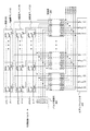
- 相対的に原稿を副走査方向に走査する際に前記副走査方向に異なる色の画素アレイが配列され、各画素アレイが光電変換を行う複数の画素を有する複数の画素アレイと、
前記画素の動作を制御する制御パルスのパルス位置を制御するパルス制御部とを有し、
前記パルス制御部は、各色の前記画素アレイの副走査方向の色ズレ量に応じて、前記各色の画素アレイの制御パルスのパルス位置を制御し、
さらに、前記複数の画素アレイに電源電圧を供給する電源配線を有し、
前記電源配線は、前記異なる色の画素アレイの間で分離されていることを特徴とする光電変換装置。 - 前記パルス制御部は、前記画素の光電変換による電荷蓄積期間を制御する制御パルスを生成することを特徴とする請求項1記載の光電変換装置。
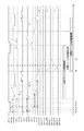
- 前記制御パルスは、前記画素のリセット動作を制御するリセットパルスと、前記画素の電荷蓄積期間を決める電荷の転送動作を制御する転送パルスと、前記画素の信号のサンプルホールド動作を制御する読み出しパルスとを含むことを特徴とする請求項1又は2記載の光電変換装置。
- 前記パルス制御部は、前記リセットパルスと前記転送パルスと前記読み出しパルスのパルス位置の変化量を、色単位の一律の色ズレ量で制御することを特徴とする請求項3記載の光電変換装置。
- さらに、前記複数の画素アレイが補正用パターン画像を走査した時の前記副走査方向の色ズレ量を算出する色ズレ量算出部を有し、
前記パルス制御部は、前記色ズレ量算出部により算出された色ズレ量に応じて、前記各色の画素アレイの制御パルスのパルス位置を制御することを特徴とする請求項1〜4のいずれか1項に記載の光電変換装置。 - 前記複数の画素アレイは、メタルによって入射光を遮断するオプティカルブラック画素を有し、
前記メタルは、前記電源配線とは分離されていることを特徴とする請求項1〜5のいずれか1項に記載の光電変換装置。
Priority Applications (1)
| Application Number | Priority Date | Filing Date | Title |
|---|---|---|---|
| JP2013029031A JP6132583B2 (ja) | 2012-02-29 | 2013-02-18 | 光電変換装置 |
Applications Claiming Priority (3)
| Application Number | Priority Date | Filing Date | Title |
|---|---|---|---|
| JP2012043765 | 2012-02-29 | ||
| JP2012043765 | 2012-02-29 | ||
| JP2013029031A JP6132583B2 (ja) | 2012-02-29 | 2013-02-18 | 光電変換装置 |
Publications (2)
| Publication Number | Publication Date |
|---|---|
| JP2013211838A JP2013211838A (ja) | 2013-10-10 |
| JP6132583B2 true JP6132583B2 (ja) | 2017-05-24 |
Family
ID=49001810
Family Applications (1)
| Application Number | Title | Priority Date | Filing Date |
|---|---|---|---|
| JP2013029031A Expired - Fee Related JP6132583B2 (ja) | 2012-02-29 | 2013-02-18 | 光電変換装置 |
Country Status (2)
| Country | Link |
|---|---|
| US (2) | US9197833B2 (ja) |
| JP (1) | JP6132583B2 (ja) |
Families Citing this family (14)
| Publication number | Priority date | Publication date | Assignee | Title |
|---|---|---|---|---|
| JP6041531B2 (ja) | 2012-05-24 | 2016-12-07 | キヤノン株式会社 | 光電変換装置 |
| JP2014175553A (ja) | 2013-03-11 | 2014-09-22 | Canon Inc | 固体撮像装置およびカメラ |
| JP6265694B2 (ja) | 2013-11-12 | 2018-01-24 | キヤノン株式会社 | 固体撮像装置及び撮像システム |
| JP6478717B2 (ja) * | 2014-11-21 | 2019-03-06 | キヤノン株式会社 | 撮像装置及び撮像システム |
| JP6595793B2 (ja) | 2015-04-13 | 2019-10-23 | キヤノン株式会社 | 光電変換装置、その駆動方法、焦点検出センサ及び撮像システム |
| JP2017139431A (ja) | 2016-02-05 | 2017-08-10 | キヤノン株式会社 | 固体撮像装置及びその製造方法 |
| EP3432565B1 (en) * | 2016-03-16 | 2020-07-08 | Ricoh Company, Ltd. | Photoelectric conversion device, image reading device, and image forming device |
| JP6766462B2 (ja) | 2016-06-16 | 2020-10-14 | セイコーエプソン株式会社 | スキャナー、スキャン画像の生産方法 |
| JP6834809B2 (ja) * | 2017-06-27 | 2021-02-24 | 株式会社リコー | 撮像装置および撮像方法 |
| JP7483454B2 (ja) | 2020-03-26 | 2024-05-15 | キヤノン株式会社 | 光電変換装置、撮像システム、移動体 |
| JP7171649B2 (ja) | 2020-05-15 | 2022-11-15 | キヤノン株式会社 | 撮像装置および撮像システム |
| JP7606370B2 (ja) * | 2021-03-10 | 2024-12-25 | キヤノン株式会社 | 光電変換装置及び光電変換装置の制御方法 |
| JP7467380B2 (ja) * | 2021-03-18 | 2024-04-15 | 株式会社東芝 | 固体撮像装置 |
| US11900859B2 (en) * | 2021-05-21 | 2024-02-13 | Lumileds Llc | Active matrix hybrid microLED display |
Family Cites Families (11)
| Publication number | Priority date | Publication date | Assignee | Title |
|---|---|---|---|---|
| JPH05122542A (ja) | 1991-10-23 | 1993-05-18 | Canon Inc | 画像処理装置 |
| JPH05284374A (ja) * | 1992-03-31 | 1993-10-29 | Ricoh Co Ltd | カラー画像処理装置 |
| JP3715969B2 (ja) * | 2003-03-05 | 2005-11-16 | キヤノン株式会社 | 色信号補正装置及び画像表示装置 |
| JP2006005592A (ja) * | 2004-06-16 | 2006-01-05 | Konica Minolta Business Technologies Inc | 画像読取装置、画像読取方法及び画像形成装置 |
| JP4194633B2 (ja) | 2006-08-08 | 2008-12-10 | キヤノン株式会社 | 撮像装置及び撮像システム |
| JP5347341B2 (ja) * | 2008-06-06 | 2013-11-20 | ソニー株式会社 | 固体撮像装置、撮像装置、電子機器、ad変換装置、ad変換方法 |
| JP5374082B2 (ja) | 2008-07-09 | 2013-12-25 | キヤノン株式会社 | 撮像装置及び撮像システム |
| JP5288965B2 (ja) * | 2008-09-22 | 2013-09-11 | キヤノン株式会社 | 固体撮像装置及びその駆動方法 |
| JP5322696B2 (ja) | 2009-02-25 | 2013-10-23 | キヤノン株式会社 | 固体撮像装置及びその駆動方法 |
| JP6041531B2 (ja) | 2012-05-24 | 2016-12-07 | キヤノン株式会社 | 光電変換装置 |
| CN105706434B (zh) * | 2013-11-15 | 2019-01-08 | 富士胶片株式会社 | 颜色转换表制作装置及方法 |
-
2013
- 2013-02-18 JP JP2013029031A patent/JP6132583B2/ja not_active Expired - Fee Related
- 2013-02-21 US US13/773,121 patent/US9197833B2/en not_active Expired - Fee Related
-
2015
- 2015-10-21 US US14/918,799 patent/US9813681B2/en not_active Expired - Fee Related
Also Published As
| Publication number | Publication date |
|---|---|
| US20160044288A1 (en) | 2016-02-11 |
| US9813681B2 (en) | 2017-11-07 |
| JP2013211838A (ja) | 2013-10-10 |
| US20130221199A1 (en) | 2013-08-29 |
| US9197833B2 (en) | 2015-11-24 |
Similar Documents
| Publication | Publication Date | Title |
|---|---|---|
| JP6132583B2 (ja) | 光電変換装置 | |
| TWI726070B (zh) | 固體攝像元件 | |
| US8289431B2 (en) | Image sensing device and image sensing system | |
| JP6776011B2 (ja) | 撮像装置及び撮像システム | |
| US8120681B2 (en) | Image sensing apparatus, image sensing apparatus control method, and imaging system | |
| EP2832090B1 (en) | Cmos image sensors implementing full frame digital correlated double sampling with global shutter | |
| CN101959014B (zh) | 摄像设备及其控制方法 | |
| US8780236B2 (en) | Imaging apparatus for correcting noise when a quantity of pixels in an invalid pixel area is small | |
| CN104243862B (zh) | 固态图像传感器 | |
| JP6041531B2 (ja) | 光電変換装置 | |
| JP2002507340A (ja) | 改善された充填比を有するcmos画像センサ | |
| US9659982B2 (en) | Image sensor pixel structure with optimized uniformity | |
| US9426391B2 (en) | Solid-state imaging apparatus, method of controlling the same, and imaging system | |
| US9001246B2 (en) | Imaging apparatus, an imaging system, and a driving method of an imaging apparatus using correction data applied to pixels of same color | |
| JP2009206941A (ja) | 撮像装置及び撮像装置を用いた撮像システム | |
| US7787036B2 (en) | Imaging apparatus configured to correct noise | |
| JP2015002415A (ja) | 光電変換装置、光電変換システム、光電変換装置の駆動方法 | |
| US10863130B2 (en) | Backside illuminated global shutter imaging array | |
| US9294692B2 (en) | Image pickup apparatus having photoelectric coversion units, method of driving image pickup apparatus, and method of driving image pickup system | |
| US9838591B2 (en) | Imaging apparatus and imaging system for generating a signal for focus detection | |
| JP6257348B2 (ja) | 固体撮像装置、撮像システム及び複写機 | |
| JP5436642B2 (ja) | 撮像装置及び撮像装置を用いた撮像システム | |
| JP2009296451A (ja) | 固体撮像装置 | |
| JP2012015919A (ja) | 固体撮像装置及びそれを用いた撮像装置 |
Legal Events
| Date | Code | Title | Description |
|---|---|---|---|
| A621 | Written request for application examination |
Free format text: JAPANESE INTERMEDIATE CODE: A621 Effective date: 20160218 |
|
| A977 | Report on retrieval |
Free format text: JAPANESE INTERMEDIATE CODE: A971007 Effective date: 20161222 |
|
| A131 | Notification of reasons for refusal |
Free format text: JAPANESE INTERMEDIATE CODE: A131 Effective date: 20170110 |
|
| A521 | Request for written amendment filed |
Free format text: JAPANESE INTERMEDIATE CODE: A523 Effective date: 20170308 |
|
| TRDD | Decision of grant or rejection written | ||
| A01 | Written decision to grant a patent or to grant a registration (utility model) |
Free format text: JAPANESE INTERMEDIATE CODE: A01 Effective date: 20170321 |
|
| A61 | First payment of annual fees (during grant procedure) |
Free format text: JAPANESE INTERMEDIATE CODE: A61 Effective date: 20170418 |
|
| R151 | Written notification of patent or utility model registration |
Ref document number: 6132583 Country of ref document: JP Free format text: JAPANESE INTERMEDIATE CODE: R151 |
|
| LAPS | Cancellation because of no payment of annual fees |