JP6257348B2 - 固体撮像装置、撮像システム及び複写機 - Google Patents
固体撮像装置、撮像システム及び複写機 Download PDFInfo
- Publication number
- JP6257348B2 JP6257348B2 JP2014008802A JP2014008802A JP6257348B2 JP 6257348 B2 JP6257348 B2 JP 6257348B2 JP 2014008802 A JP2014008802 A JP 2014008802A JP 2014008802 A JP2014008802 A JP 2014008802A JP 6257348 B2 JP6257348 B2 JP 6257348B2
- Authority
- JP
- Japan
- Prior art keywords
- photoelectric conversion
- solid
- imaging device
- state imaging
- conversion unit
- Prior art date
- Legal status (The legal status is an assumption and is not a legal conclusion. Google has not performed a legal analysis and makes no representation as to the accuracy of the status listed.)
- Expired - Fee Related
Links
- 238000003384 imaging method Methods 0.000 title claims description 64
- 238000006243 chemical reaction Methods 0.000 claims description 52
- 238000009825 accumulation Methods 0.000 claims description 38
- 238000012546 transfer Methods 0.000 claims description 34
- 238000009792 diffusion process Methods 0.000 claims description 26
- 238000012545 processing Methods 0.000 claims description 24
- 238000000034 method Methods 0.000 claims description 14
- 230000008569 process Effects 0.000 claims description 6
- 239000004065 semiconductor Substances 0.000 claims description 2
- 239000000758 substrate Substances 0.000 claims description 2
- 239000011295 pitch Substances 0.000 description 25
- 238000010586 diagram Methods 0.000 description 11
- 230000005484 gravity Effects 0.000 description 8
- 230000003321 amplification Effects 0.000 description 7
- 238000003199 nucleic acid amplification method Methods 0.000 description 7
- 230000003287 optical effect Effects 0.000 description 7
- 230000004044 response Effects 0.000 description 6
- 238000004891 communication Methods 0.000 description 5
- 238000012937 correction Methods 0.000 description 3
- 230000004075 alteration Effects 0.000 description 2
- 230000008859 change Effects 0.000 description 2
- 230000000694 effects Effects 0.000 description 2
- 230000035945 sensitivity Effects 0.000 description 2
- 230000003595 spectral effect Effects 0.000 description 2
- 239000003086 colorant Substances 0.000 description 1
- 230000010485 coping Effects 0.000 description 1
- 230000006866 deterioration Effects 0.000 description 1
- 238000006073 displacement reaction Methods 0.000 description 1
- 230000006870 function Effects 0.000 description 1
- 230000009467 reduction Effects 0.000 description 1
- 238000003530 single readout Methods 0.000 description 1
- 238000005549 size reduction Methods 0.000 description 1
- 230000006641 stabilisation Effects 0.000 description 1
- 238000011105 stabilization Methods 0.000 description 1
- 230000002194 synthesizing effect Effects 0.000 description 1
Images


Classifications
-
- H—ELECTRICITY
- H04—ELECTRIC COMMUNICATION TECHNIQUE
- H04N—PICTORIAL COMMUNICATION, e.g. TELEVISION
- H04N1/00—Scanning, transmission or reproduction of documents or the like, e.g. facsimile transmission; Details thereof
- H04N1/024—Details of scanning heads ; Means for illuminating the original
- H04N1/028—Details of scanning heads ; Means for illuminating the original for picture information pick-up
-
- H—ELECTRICITY
- H01—ELECTRIC ELEMENTS
- H01L—SEMICONDUCTOR DEVICES NOT COVERED BY CLASS H10
- H01L27/00—Devices consisting of a plurality of semiconductor or other solid-state components formed in or on a common substrate
- H01L27/14—Devices consisting of a plurality of semiconductor or other solid-state components formed in or on a common substrate including semiconductor components sensitive to infrared radiation, light, electromagnetic radiation of shorter wavelength or corpuscular radiation and specially adapted either for the conversion of the energy of such radiation into electrical energy or for the control of electrical energy by such radiation
- H01L27/144—Devices controlled by radiation
- H01L27/146—Imager structures
- H01L27/14601—Structural or functional details thereof
- H01L27/14603—Special geometry or disposition of pixel-elements, address-lines or gate-electrodes
-
- H—ELECTRICITY
- H01—ELECTRIC ELEMENTS
- H01L—SEMICONDUCTOR DEVICES NOT COVERED BY CLASS H10
- H01L27/00—Devices consisting of a plurality of semiconductor or other solid-state components formed in or on a common substrate
- H01L27/14—Devices consisting of a plurality of semiconductor or other solid-state components formed in or on a common substrate including semiconductor components sensitive to infrared radiation, light, electromagnetic radiation of shorter wavelength or corpuscular radiation and specially adapted either for the conversion of the energy of such radiation into electrical energy or for the control of electrical energy by such radiation
- H01L27/144—Devices controlled by radiation
- H01L27/146—Imager structures
- H01L27/14601—Structural or functional details thereof
- H01L27/14641—Electronic components shared by two or more pixel-elements, e.g. one amplifier shared by two pixel elements
-
- H—ELECTRICITY
- H01—ELECTRIC ELEMENTS
- H01L—SEMICONDUCTOR DEVICES NOT COVERED BY CLASS H10
- H01L27/00—Devices consisting of a plurality of semiconductor or other solid-state components formed in or on a common substrate
- H01L27/14—Devices consisting of a plurality of semiconductor or other solid-state components formed in or on a common substrate including semiconductor components sensitive to infrared radiation, light, electromagnetic radiation of shorter wavelength or corpuscular radiation and specially adapted either for the conversion of the energy of such radiation into electrical energy or for the control of electrical energy by such radiation
- H01L27/144—Devices controlled by radiation
- H01L27/146—Imager structures
- H01L27/14643—Photodiode arrays; MOS imagers
Description
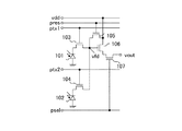
図1は、本発明の第1の実施形態による固体撮像装置の構成例を示す図である。画素アレイ100は、1次元に配列された複数の画素セル110を有し、入射光に応じた複数の画素信号を出力する。複数の電流源200は、それぞれ、複数の画素セル110内の増幅器を所定の動作点で動作させるための電流源である。信号処理回路300は、画素アレイ100から入力した画素信号を処理し、外部出力線400へ出力する。固体撮像装置は、例えば、複写機等に用いられるラインセンサであり、原稿に対して相対的に走査されることにより、2次元画像を生成することができる。複写機は、固体撮像装置と、固体撮像装置が出力する信号を処理する信号処理部とを備える。複写機は、固体撮像装置が出力する信号を信号処理部が処理した信号を用いて、印刷を行う。
y={n+(b/a)}×x (1)
y={n+(b/a)+c}×x (2)
y12={n+(b12/a)}×x (3)
y23={n+(b23/a)}×x (4)
ymr=n×x (5)
yrg=n×x (6)
ygb={n+(b/a)}×x (7)
図13は、本発明の第2の実施形態による固体撮像装置の構成例を示す図である。以下、本実施形態が第1の実施形態と異なる点を説明する。画素セル110は、主走査方向に対して配列される2個の画素を共有している。また、副走査方向には、2個の画素セル110が配列されている。
y=(b/a)×x (8)
y={(b/a)+c}×x (9)
図15は、本発明の第3の実施形態による撮像システムの構成例を示す図である。撮像システム800は、例えば、光学部810、撮像装置1000、映像信号処理回路部830、記録・通信部840、タイミング制御回路部850、システムコントロール回路部860、及び再生・表示部870を含む。撮像装置1000としては、第1及び第2の実施形態で述べた固体撮像装置を用いることができる。
Claims (10)
- 複数のセルとメモリとを有し、原稿に対して第1の方向で相対的に走査される固体撮像装置であって、
前記複数のセルの各々は、
光を電荷に変換して蓄積する第1の光電変換部と、
前記第1の光電変換部に対して前記第1の方向に配置された、光を電荷に変換して蓄積する第2の光電変換部とを有し、
前記メモリは、前記第1及び第2の光電変換部に対して共通に設けられ、前記第1及び第2の光電変換部の各々が蓄積した電荷もしくは前記電荷に基づく信号を保持し、
前記第1及び第2の光電変換部の電荷蓄積を終了するタイミングのずれをbとし、前記第1及び第2の光電変換部が電荷蓄積を終了してから再び電荷蓄積を行って次に電荷蓄積を終了するまでの期間をaとし、nを1以上の整数とし、前記複数のセルのうちの一のセルの前記第1の光電変換部と、前記一のセルと前記第1の方向に対して直交する第2の方向で隣接する別のセルの前記第1の光電変換部との間隔をxとした場合に、前記一のセルの前記第1及び第2の光電変換部の前記第1の方向の間隔は、{n+(b/a)}×xであることを特徴とする固体撮像装置。 - 前記第1及び第2の光電変換部の前記第1の方向の間隔は、{n+(b/a)+c}×xであり、cの絶対値が0.1以上0.15以下の値であることを特徴とする請求項1記載の固体撮像装置。
- 複数のセルとメモリとを有し、原稿に対して第1の方向で相対的に走査される固体撮像装置であって、
前記複数のセルの各々は、
光を電荷に変換して蓄積する第1の光電変換部と、
前記第1の光電変換部に対して前記第1の方向とは直交する第2の方向に配置された、光を電荷に変換して蓄積する第2の光電変換部とを有し、
前記メモリは、前記第1及び第2の光電変換部に対して共通に設けられ、前記第1及び第2の光電変換部の各々が蓄積した電荷もしくは前記電荷に基づく信号を保持し、
前記第1及び第2の光電変換部の電荷蓄積を終了するタイミングのずれをbとし、前記第1及び第2の光電変換部が電荷蓄積を終了してから再び電荷蓄積を行って次に電荷蓄積を終了するまでの期間をaとし、同一セルの前記第1の光電変換部と前記第2の光電変換部との間隔をxとした場合に、前記同一セルの前記第1の光電変換部と前記第2の光電変換部との前記第1の方向の間隔は、(b/a)×xであることを特徴とする固体撮像装置。 - 前記同一セルの前記第1の光電変換部と前記第2の光電変換部との前記第1の方向の間隔は、{(b/a)+c}×xであり、cの絶対値が0.1以上0.15以下の値であることを特徴とする請求項3記載の固体撮像装置。
- 前記複数のセルの各々は、前記メモリとして、前記第1及び第2の光電変換部の各々が蓄積した電荷を保持するフローティングディフュージョンをさらに有することを特徴とする請求項1〜4のいずれか1項に記載の固体撮像装置。
- 前記複数のセルの各々は、前記フローティングディフュージョンをリセット電位にリセットするためのリセットトランジスタをさらに有することを特徴とする請求項5記載の固体撮像装置。
- 前記複数のセルの各々は、前記第1の光電変換部が蓄積した電荷を前記フローティングディフュージョンに転送する第1の転送トランジスタと、前記第2の光電変換部が蓄積した電荷を前記フローティングディフュージョンに転送する第2の転送トランジスタとをさらに有し、
前記第1及び第2の光電変換部の電荷蓄積を終了するタイミングのずれは、前記第1の転送トランジスタが前記第1の光電変換部から前記フローティングディフュージョンへの前記電荷の転送を終了するタイミングと、前記第2の転送トランジスタが前記第2の光電変換部から前記フローティングディフュージョンへの前記電荷の転送を終了するタイミングとのずれであることを特徴とする請求項5又は6記載の固体撮像装置。 - 前記複数のセルは、同一の半導体基板に設けられることを特徴とする請求項1〜7のいずれか1項に記載の固体撮像装置。
- 請求項1〜8のいずれか1項に記載の固体撮像装置と、
前記固体撮像装置の出力信号を処理する信号処理部と
を有することを特徴とする撮像システム。 - 請求項1〜8のいずれか1項に記載の固体撮像装置と、
前記固体撮像装置の出力信号を処理する信号処理部とを有し、
前記信号処理部が処理した信号を用いて、印刷を行うことを特徴とする複写機。
Priority Applications (2)
| Application Number | Priority Date | Filing Date | Title |
|---|---|---|---|
| JP2014008802A JP6257348B2 (ja) | 2014-01-21 | 2014-01-21 | 固体撮像装置、撮像システム及び複写機 |
| US14/601,025 US20150206910A1 (en) | 2014-01-21 | 2015-01-20 | Solid-state imaging device, imaging system, and copier |
Applications Claiming Priority (1)
| Application Number | Priority Date | Filing Date | Title |
|---|---|---|---|
| JP2014008802A JP6257348B2 (ja) | 2014-01-21 | 2014-01-21 | 固体撮像装置、撮像システム及び複写機 |
Publications (2)
| Publication Number | Publication Date |
|---|---|
| JP2015139054A JP2015139054A (ja) | 2015-07-30 |
| JP6257348B2 true JP6257348B2 (ja) | 2018-01-10 |
Family
ID=53545516
Family Applications (1)
| Application Number | Title | Priority Date | Filing Date |
|---|---|---|---|
| JP2014008802A Expired - Fee Related JP6257348B2 (ja) | 2014-01-21 | 2014-01-21 | 固体撮像装置、撮像システム及び複写機 |
Country Status (2)
| Country | Link |
|---|---|
| US (1) | US20150206910A1 (ja) |
| JP (1) | JP6257348B2 (ja) |
Families Citing this family (2)
| Publication number | Priority date | Publication date | Assignee | Title |
|---|---|---|---|---|
| JP6042737B2 (ja) * | 2013-01-31 | 2016-12-14 | オリンパス株式会社 | 固体撮像装置および撮像装置 |
| CN110444005A (zh) * | 2019-08-08 | 2019-11-12 | 国网新疆电力有限公司电力科学研究院 | 低压电力线载波抄表系统抗干扰性能测试方法及系统 |
Family Cites Families (4)
| Publication number | Priority date | Publication date | Assignee | Title |
|---|---|---|---|---|
| JP4179329B2 (ja) * | 2006-03-17 | 2008-11-12 | セイコーエプソン株式会社 | ラインセンサチップ、ラインセンサ、画像情報読取装置、ファクシミリ、スキャナ及び複写機 |
| JP4858281B2 (ja) * | 2006-05-16 | 2012-01-18 | コニカミノルタホールディングス株式会社 | 固体撮像装置 |
| JP2011239261A (ja) * | 2010-05-12 | 2011-11-24 | Konica Minolta Business Technologies Inc | 固体撮像装置 |
| JP2012060493A (ja) * | 2010-09-10 | 2012-03-22 | Canon Inc | 画像読取装置 |
-
2014
- 2014-01-21 JP JP2014008802A patent/JP6257348B2/ja not_active Expired - Fee Related
-
2015
- 2015-01-20 US US14/601,025 patent/US20150206910A1/en not_active Abandoned
Also Published As
| Publication number | Publication date |
|---|---|
| JP2015139054A (ja) | 2015-07-30 |
| US20150206910A1 (en) | 2015-07-23 |
Similar Documents
| Publication | Publication Date | Title |
|---|---|---|
| US7982789B2 (en) | Image sensing apparatus driving method, image sensing apparatus, and image sensing system | |
| US9319614B2 (en) | Image pickup device with a group of focus detection pixels associated with a dedicated readout circuit and image pickup apparatus including the image pickup device | |
| US9036052B2 (en) | Image pickup apparatus that uses pixels different in sensitivity, method of controlling the same, and storage medium | |
| US20150189249A1 (en) | Solid state imaging apparatus and imaging system using the same | |
| US10477165B2 (en) | Solid-state imaging apparatus, driving method therefor, and imaging system | |
| JP6445866B2 (ja) | 撮像装置、撮像システム、および撮像装置の駆動方法 | |
| JP6164867B2 (ja) | 固体撮像装置、その制御方法、および制御プログラム | |
| JP2014160930A (ja) | 固体撮像素子およびその駆動方法、並びに電子機器 | |
| JP2007336519A (ja) | 固体撮像装置 | |
| JP6872956B2 (ja) | 撮像システム及び撮像システムの制御方法 | |
| US10362252B2 (en) | Solid-state image sensor, image capturing apparatus and control method thereof, and storage medium | |
| JP5721518B2 (ja) | 撮像素子及び撮像装置 | |
| WO2011083541A1 (ja) | 固体撮像装置および撮像装置 | |
| JP6265694B2 (ja) | 固体撮像装置及び撮像システム | |
| JP2008278453A (ja) | 撮像装置及び撮像システム | |
| JP6257348B2 (ja) | 固体撮像装置、撮像システム及び複写機 | |
| WO2013084808A1 (ja) | 固体撮像素子およびその駆動方法、カメラシステム | |
| US9838591B2 (en) | Imaging apparatus and imaging system for generating a signal for focus detection | |
| JP6700850B2 (ja) | 撮像素子の駆動制御回路 | |
| JP5511205B2 (ja) | 撮像装置及び撮像方法 | |
| JP2009225341A (ja) | 固体撮像装置及びその駆動方法 | |
| JP2023156437A (ja) | 撮像素子 | |
| JP2015173387A (ja) | 撮像素子、その駆動方法、およびプログラム | |
| JP2019165274A (ja) | 固体撮像素子及び撮像装置 | |
| JP2017157929A (ja) | 固体撮像装置及び画像読取装置 |
Legal Events
| Date | Code | Title | Description |
|---|---|---|---|
| A621 | Written request for application examination |
Free format text: JAPANESE INTERMEDIATE CODE: A621 Effective date: 20170110 |
|
| A977 | Report on retrieval |
Free format text: JAPANESE INTERMEDIATE CODE: A971007 Effective date: 20171012 |
|
| TRDD | Decision of grant or rejection written | ||
| A01 | Written decision to grant a patent or to grant a registration (utility model) |
Free format text: JAPANESE INTERMEDIATE CODE: A01 Effective date: 20171107 |
|
| A61 | First payment of annual fees (during grant procedure) |
Free format text: JAPANESE INTERMEDIATE CODE: A61 Effective date: 20171205 |
|
| R151 | Written notification of patent or utility model registration |
Ref document number: 6257348 Country of ref document: JP Free format text: JAPANESE INTERMEDIATE CODE: R151 |
|
| LAPS | Cancellation because of no payment of annual fees |