JP6128046B2 - 実装基板および電子機器 - Google Patents
実装基板および電子機器 Download PDFInfo
- Publication number
- JP6128046B2 JP6128046B2 JP2014074844A JP2014074844A JP6128046B2 JP 6128046 B2 JP6128046 B2 JP 6128046B2 JP 2014074844 A JP2014074844 A JP 2014074844A JP 2014074844 A JP2014074844 A JP 2014074844A JP 6128046 B2 JP6128046 B2 JP 6128046B2
- Authority
- JP
- Japan
- Prior art keywords
- wiring
- layer
- wirings
- wiring board
- board
- Prior art date
- Legal status (The legal status is an assumption and is not a legal conclusion. Google has not performed a legal analysis and makes no representation as to the accuracy of the status listed.)
- Active
Links
- 239000000758 substrate Substances 0.000 claims description 123
- 239000011159 matrix material Substances 0.000 claims description 9
- 239000010410 layer Substances 0.000 description 213
- 101100537098 Mus musculus Alyref gene Proteins 0.000 description 22
- 101150095908 apex1 gene Proteins 0.000 description 22
- 102100036285 25-hydroxyvitamin D-1 alpha hydroxylase, mitochondrial Human genes 0.000 description 21
- 101000875403 Homo sapiens 25-hydroxyvitamin D-1 alpha hydroxylase, mitochondrial Proteins 0.000 description 21
- 101100269674 Mus musculus Alyref2 gene Proteins 0.000 description 21
- 238000005516 engineering process Methods 0.000 description 21
- 238000000034 method Methods 0.000 description 21
- 230000004048 modification Effects 0.000 description 18
- 238000012986 modification Methods 0.000 description 18
- 238000007747 plating Methods 0.000 description 16
- 238000010586 diagram Methods 0.000 description 10
- 230000000694 effects Effects 0.000 description 10
- 239000011347 resin Substances 0.000 description 9
- 229920005989 resin Polymers 0.000 description 9
- 238000005286 illumination Methods 0.000 description 8
- 239000003086 colorant Substances 0.000 description 6
- 238000004519 manufacturing process Methods 0.000 description 6
- RYGMFSIKBFXOCR-UHFFFAOYSA-N Copper Chemical compound [Cu] RYGMFSIKBFXOCR-UHFFFAOYSA-N 0.000 description 5
- 229910052802 copper Inorganic materials 0.000 description 5
- 239000010949 copper Substances 0.000 description 5
- 230000015572 biosynthetic process Effects 0.000 description 4
- 239000011521 glass Substances 0.000 description 4
- 239000000853 adhesive Substances 0.000 description 3
- 230000001070 adhesive effect Effects 0.000 description 3
- 230000000052 comparative effect Effects 0.000 description 3
- 239000002184 metal Substances 0.000 description 3
- 229910052751 metal Inorganic materials 0.000 description 3
- 239000000203 mixture Substances 0.000 description 3
- 239000004065 semiconductor Substances 0.000 description 3
- 239000000463 material Substances 0.000 description 2
- 229910000679 solder Inorganic materials 0.000 description 2
- 238000004544 sputter deposition Methods 0.000 description 2
- 229920001187 thermosetting polymer Polymers 0.000 description 2
- 239000004593 Epoxy Substances 0.000 description 1
- 239000004820 Pressure-sensitive adhesive Substances 0.000 description 1
- 229910000831 Steel Inorganic materials 0.000 description 1
- 208000004350 Strabismus Diseases 0.000 description 1
- NIXOWILDQLNWCW-UHFFFAOYSA-N acrylic acid group Chemical group C(C=C)(=O)O NIXOWILDQLNWCW-UHFFFAOYSA-N 0.000 description 1
- 238000001312 dry etching Methods 0.000 description 1
- 238000007654 immersion Methods 0.000 description 1
- 239000003960 organic solvent Substances 0.000 description 1
- 229920001296 polysiloxane Polymers 0.000 description 1
- 230000001681 protective effect Effects 0.000 description 1
- 230000001012 protector Effects 0.000 description 1
- 238000005070 sampling Methods 0.000 description 1
- 239000010959 steel Substances 0.000 description 1
Images


Classifications
-
- H—ELECTRICITY
- H01—ELECTRIC ELEMENTS
- H01L—SEMICONDUCTOR DEVICES NOT COVERED BY CLASS H10
- H01L23/00—Details of semiconductor or other solid state devices
- H01L23/52—Arrangements for conducting electric current within the device in operation from one component to another, i.e. interconnections, e.g. wires, lead frames
- H01L23/538—Arrangements for conducting electric current within the device in operation from one component to another, i.e. interconnections, e.g. wires, lead frames the interconnection structure between a plurality of semiconductor chips being formed on, or in, insulating substrates
- H01L23/5386—Geometry or layout of the interconnection structure
-
- H—ELECTRICITY
- H01—ELECTRIC ELEMENTS
- H01L—SEMICONDUCTOR DEVICES NOT COVERED BY CLASS H10
- H01L21/00—Processes or apparatus adapted for the manufacture or treatment of semiconductor or solid state devices or of parts thereof
- H01L21/02—Manufacture or treatment of semiconductor devices or of parts thereof
- H01L21/04—Manufacture or treatment of semiconductor devices or of parts thereof the devices having at least one potential-jump barrier or surface barrier, e.g. PN junction, depletion layer or carrier concentration layer
- H01L21/48—Manufacture or treatment of parts, e.g. containers, prior to assembly of the devices, using processes not provided for in a single one of the subgroups H01L21/06 - H01L21/326
- H01L21/4814—Conductive parts
- H01L21/4846—Leads on or in insulating or insulated substrates, e.g. metallisation
- H01L21/4853—Connection or disconnection of other leads to or from a metallisation, e.g. pins, wires, bumps
-
- H—ELECTRICITY
- H01—ELECTRIC ELEMENTS
- H01L—SEMICONDUCTOR DEVICES NOT COVERED BY CLASS H10
- H01L21/00—Processes or apparatus adapted for the manufacture or treatment of semiconductor or solid state devices or of parts thereof
- H01L21/02—Manufacture or treatment of semiconductor devices or of parts thereof
- H01L21/04—Manufacture or treatment of semiconductor devices or of parts thereof the devices having at least one potential-jump barrier or surface barrier, e.g. PN junction, depletion layer or carrier concentration layer
- H01L21/48—Manufacture or treatment of parts, e.g. containers, prior to assembly of the devices, using processes not provided for in a single one of the subgroups H01L21/06 - H01L21/326
- H01L21/4814—Conductive parts
- H01L21/4846—Leads on or in insulating or insulated substrates, e.g. metallisation
- H01L21/4857—Multilayer substrates
-
- H—ELECTRICITY
- H01—ELECTRIC ELEMENTS
- H01L—SEMICONDUCTOR DEVICES NOT COVERED BY CLASS H10
- H01L21/00—Processes or apparatus adapted for the manufacture or treatment of semiconductor or solid state devices or of parts thereof
- H01L21/02—Manufacture or treatment of semiconductor devices or of parts thereof
- H01L21/04—Manufacture or treatment of semiconductor devices or of parts thereof the devices having at least one potential-jump barrier or surface barrier, e.g. PN junction, depletion layer or carrier concentration layer
- H01L21/48—Manufacture or treatment of parts, e.g. containers, prior to assembly of the devices, using processes not provided for in a single one of the subgroups H01L21/06 - H01L21/326
- H01L21/4814—Conductive parts
- H01L21/4846—Leads on or in insulating or insulated substrates, e.g. metallisation
- H01L21/486—Via connections through the substrate with or without pins
-
- H—ELECTRICITY
- H01—ELECTRIC ELEMENTS
- H01L—SEMICONDUCTOR DEVICES NOT COVERED BY CLASS H10
- H01L23/00—Details of semiconductor or other solid state devices
- H01L23/52—Arrangements for conducting electric current within the device in operation from one component to another, i.e. interconnections, e.g. wires, lead frames
- H01L23/538—Arrangements for conducting electric current within the device in operation from one component to another, i.e. interconnections, e.g. wires, lead frames the interconnection structure between a plurality of semiconductor chips being formed on, or in, insulating substrates
- H01L23/5383—Multilayer substrates
-
- H—ELECTRICITY
- H01—ELECTRIC ELEMENTS
- H01L—SEMICONDUCTOR DEVICES NOT COVERED BY CLASS H10
- H01L23/00—Details of semiconductor or other solid state devices
- H01L23/52—Arrangements for conducting electric current within the device in operation from one component to another, i.e. interconnections, e.g. wires, lead frames
- H01L23/538—Arrangements for conducting electric current within the device in operation from one component to another, i.e. interconnections, e.g. wires, lead frames the interconnection structure between a plurality of semiconductor chips being formed on, or in, insulating substrates
- H01L23/5384—Conductive vias through the substrate with or without pins, e.g. buried coaxial conductors
-
- H—ELECTRICITY
- H01—ELECTRIC ELEMENTS
- H01L—SEMICONDUCTOR DEVICES NOT COVERED BY CLASS H10
- H01L25/00—Assemblies consisting of a plurality of individual semiconductor or other solid state devices ; Multistep manufacturing processes thereof
- H01L25/16—Assemblies consisting of a plurality of individual semiconductor or other solid state devices ; Multistep manufacturing processes thereof the devices being of types provided for in two or more different main groups of groups H01L27/00 - H01L33/00, or in a single subclass of H10K, H10N, e.g. forming hybrid circuits
- H01L25/167—Assemblies consisting of a plurality of individual semiconductor or other solid state devices ; Multistep manufacturing processes thereof the devices being of types provided for in two or more different main groups of groups H01L27/00 - H01L33/00, or in a single subclass of H10K, H10N, e.g. forming hybrid circuits comprising optoelectronic devices, e.g. LED, photodiodes
-
- H—ELECTRICITY
- H01—ELECTRIC ELEMENTS
- H01L—SEMICONDUCTOR DEVICES NOT COVERED BY CLASS H10
- H01L31/00—Semiconductor devices sensitive to infrared radiation, light, electromagnetic radiation of shorter wavelength or corpuscular radiation and specially adapted either for the conversion of the energy of such radiation into electrical energy or for the control of electrical energy by such radiation; Processes or apparatus specially adapted for the manufacture or treatment thereof or of parts thereof; Details thereof
- H01L31/02—Details
- H01L31/02002—Arrangements for conducting electric current to or from the device in operations
- H01L31/02005—Arrangements for conducting electric current to or from the device in operations for device characterised by at least one potential jump barrier or surface barrier
-
- H—ELECTRICITY
- H01—ELECTRIC ELEMENTS
- H01L—SEMICONDUCTOR DEVICES NOT COVERED BY CLASS H10
- H01L33/00—Semiconductor devices with at least one potential-jump barrier or surface barrier specially adapted for light emission; Processes or apparatus specially adapted for the manufacture or treatment thereof or of parts thereof; Details thereof
- H01L33/48—Semiconductor devices with at least one potential-jump barrier or surface barrier specially adapted for light emission; Processes or apparatus specially adapted for the manufacture or treatment thereof or of parts thereof; Details thereof characterised by the semiconductor body packages
- H01L33/62—Arrangements for conducting electric current to or from the semiconductor body, e.g. lead-frames, wire-bonds or solder balls
-
- H—ELECTRICITY
- H01—ELECTRIC ELEMENTS
- H01L—SEMICONDUCTOR DEVICES NOT COVERED BY CLASS H10
- H01L2924/00—Indexing scheme for arrangements or methods for connecting or disconnecting semiconductor or solid-state bodies as covered by H01L24/00
- H01L2924/0001—Technical content checked by a classifier
- H01L2924/0002—Not covered by any one of groups H01L24/00, H01L24/00 and H01L2224/00
-
- H—ELECTRICITY
- H05—ELECTRIC TECHNIQUES NOT OTHERWISE PROVIDED FOR
- H05K—PRINTED CIRCUITS; CASINGS OR CONSTRUCTIONAL DETAILS OF ELECTRIC APPARATUS; MANUFACTURE OF ASSEMBLAGES OF ELECTRICAL COMPONENTS
- H05K1/00—Printed circuits
- H05K1/18—Printed circuits structurally associated with non-printed electric components
- H05K1/182—Printed circuits structurally associated with non-printed electric components associated with components mounted in the printed circuit board, e.g. insert mounted components [IMC]
- H05K1/185—Components encapsulated in the insulating substrate of the printed circuit or incorporated in internal layers of a multilayer circuit
-
- H—ELECTRICITY
- H05—ELECTRIC TECHNIQUES NOT OTHERWISE PROVIDED FOR
- H05K—PRINTED CIRCUITS; CASINGS OR CONSTRUCTIONAL DETAILS OF ELECTRIC APPARATUS; MANUFACTURE OF ASSEMBLAGES OF ELECTRICAL COMPONENTS
- H05K2201/00—Indexing scheme relating to printed circuits covered by H05K1/00
- H05K2201/10—Details of components or other objects attached to or integrated in a printed circuit board
- H05K2201/10007—Types of components
- H05K2201/10106—Light emitting diode [LED]
-
- H—ELECTRICITY
- H05—ELECTRIC TECHNIQUES NOT OTHERWISE PROVIDED FOR
- H05K—PRINTED CIRCUITS; CASINGS OR CONSTRUCTIONAL DETAILS OF ELECTRIC APPARATUS; MANUFACTURE OF ASSEMBLAGES OF ELECTRICAL COMPONENTS
- H05K2201/00—Indexing scheme relating to printed circuits covered by H05K1/00
- H05K2201/10—Details of components or other objects attached to or integrated in a printed circuit board
- H05K2201/10007—Types of components
- H05K2201/10128—Display
-
- H—ELECTRICITY
- H05—ELECTRIC TECHNIQUES NOT OTHERWISE PROVIDED FOR
- H05K—PRINTED CIRCUITS; CASINGS OR CONSTRUCTIONAL DETAILS OF ELECTRIC APPARATUS; MANUFACTURE OF ASSEMBLAGES OF ELECTRICAL COMPONENTS
- H05K3/00—Apparatus or processes for manufacturing printed circuits
- H05K3/46—Manufacturing multilayer circuits
- H05K3/4602—Manufacturing multilayer circuits characterized by a special circuit board as base or central core whereon additional circuit layers are built or additional circuit boards are laminated
Description
1.第1の実施の形態(表示装置)
2.変形例(表示装置)
3.第2の実施の形態(照明装置)
4.変形例(照明装置)
5.第3の実施の形態(受光装置)
6.各実施の形態に共通の変形例
[構成]
図1は、本技術の第1の実施の形態に係る表示装置1の斜視構成の一例を表す。表示装置1は、いわゆるLEDディスプレイと呼ばれるものであり、表示画素としてLEDが用いられたものである。表示装置1は、例えば、図1に示したように、表示パネル10と、表示パネル10(具体的には後述するセル10E)を制御する制御回路20とを備えている。
表示パネル10は、実装基板10Aと、対向基板10Bとを互いに重ね合わせたものである。対向基板10Bの表面が映像表示面となっており、中央部分に表示領域を有し、その周囲に、非表示領域であるフレーム領域を有している。対向基板10Bは、例えば、所定の間隙を介して、実装基板10Aと対向する位置に配置されている。なお、対向基板10Bが、実装基板10Aの上面に接していてもよい。対向基板10Bは、例えば、可視光を透過する光透過性の基板を有しており、例えば、ガラス基板、透明樹脂基板、または透明樹脂フィルムなどを有している。
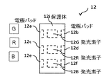
図2は、実装基板10Aの斜視構成の一例を表す。実装基板10Aは、例えば、図2に示したように、タイル状に配置された複数のユニット基板10Cで構成されている。図3は、ユニット基板10Cの斜視構成の一例を表す。ユニット基板12Cは、例えば、タイル状に配置された複数のセル10Eと、各セル10Eを支持する支持基板10Dとを有している。各ユニット基板10Cは、さらに、制御基板(図示せず)を有している。制御基板は、例えば、後述の各電極パッド34を介して、各セル10Eと電気的に接続されている。支持基板10Dは、例えば、金属フレーム、もしくは、配線基板などで構成されている。支持基板10Dが配線基板で構成されている場合には、制御基板を兼ねることも可能である。このとき、支持基板10Dおよび制御基板の少なくとも一方が、各電極パッド34を介して、各セル10E(または後述の配線基板30)と電気的に接続されている。支持基板10Dが、本技術の「支持基板」の一具体例に相当する。電極パッド34が、本技術の「電極パッド」の一具体例に相当する。
図4は、セル10Eにおける回路構成の一例を表す。セル10Eは、上述の表示領域と対向する領域に、所定の方向(具体的には列方向)に延在する複数のデータ線Sigと、所定の方向(具体的には行方向)に延在する複数のゲート線Gateとを有している。データ線Sigおよびゲート線Gateは、例えば、銅によって形成されている。データ線Sigまたはゲート線Gateが、本技術の「第1配線」の一具体例に相当する。セル10Eは、さらに、上述の表示領域と対向する領域に、行列状に配置された複数の画素11を有している。各画素11は、発光素子12と、発光素子12を駆動する駆動IC13とを含んでいる。発光素子12が、本技術の「発光素子」の一具体例に相当する。駆動IC13が、本技術の「駆動回路」の一具体例に相当する。
図7は、セル10Eの断面構成の一例を表す。図7には、セル10Eにおいて、発光素子12、駆動IC13、データ線SigB1およびゲート線Gate2の形成されている箇所の断面構成の一例が示されている。図8は、セル10Eの配線レイアウトの一例を表す。図8には、2x2行列に対応する4つの画素11に接続された配線16等の配線レイアウトの一例が示されている。各セル10Eの配線レイアウトは、例えば、図8に記載のレイアウトが行方向および列方向に繰り返し配置されたレイアウトとなっている。図8において四角で囲まれた配線名は、その配線名に隣接するビア14(後述)に電気的に接続される配線の名称を示している。
配線基板30は、例えば、層間の電気的な接続がビアでなされた積層基板である。配線基板30は、配線基板30の裏面に、外部接続端子としての複数の電極パッド34を有している。複数の電極パッド34は、例えば、データ線SigR1、データ線SigG1、データ線SigB1、ゲート線Gate1、ゲート線Gate2、電源線VDD1、参照電圧線Ref1、参照電圧線Ref2およびのこぎり電圧線Sawごとに、1つ以上設けられている。
SigR1 2 2
SigG1 1 2
SigB1 1 2
SigR2 1 2
SigG2 1 2
SigB2 1 2
VDD1 1 4
Ref1 1 4
Ref2 1 4
Gate1 1 2
Gate2 1 2
Saw 2 4
合計 14 32
微細L/S層40は、配線層42と、配線層42と配線基板30の上面との間に設けられた絶縁層41とを有している。絶縁層41は、配線層42と、配線基板30の上面とに接している。配線層42は、各配線16を含む層である。従って、絶縁層41は、各配線16と配線基板30の上面との間に設けられており、各配線16と、配線基板30の上面とに接している。絶縁層41は、各ビア14の上面と対向する位置に開口41Aを有している。絶縁層41は、ビア14と対向する位置ではなく、ビア14と電気的に接続された中継配線15と対向する位置に開口41Aを有していてもよい。絶縁層41は、さらに、上記部分電極と電気的に接続された中継配線15と対向する位置に開口41Aを有している。開口41Aの底面には、ビア14の一部、または、中継配線15の一部が露出している。絶縁層41は、例えば、VPAで形成されている。VPAは、レジストとして一般に使われるものであり、例えば、新日鉄化学社製のVPAが上市されている。絶縁層41がVPAで形成されている場合、例えば、VPAを選択的に露光・現像することによりVPAに開口41を形成することができる。
次に、図9〜図13を参照しつつ、セル10Eの製造方法の一例について説明する。図9〜図13は、セル10Eの製造過程の一例を工程順に表す。
次に、表示装置1の作用、効果について説明する。本実施の形態では、配線基板30において、層内で所定の方向に延在する配線(例えば、データ線Sig、ゲート線Gate)ごとに複数のビア14が設けられている。層内で所定の方向に延在する配線ごとに設けられた複数のビア14が、複数の画素11の配列周期の整数倍の周期で配置されている。そして、微細L/S層40上で隣り合う複数の画素11が、微細L/S層40内の1または複数の配線16を介して、共通のビア14に電気的に接続されている。このように、隣り合う複数の画素11でビア14を共有することにより、画素11ごとにビア14を設けた場合と比べて、1つの画素11あたりに必要となるビア14の数が少なくなる。その結果、配線基板30上の微細L/S層40のL/Sを、配線基板30内の複数の配線(例えば、複数のデータ線Sig、または、複数のゲート線Gate)のL/Sよりも小さくした場合に、配線基板30上の配線層42の数を1つとすることができる。従って、本実施の形態では、配線基板30上の配線層42を多層にすることなく、実装面41Sの配線ピッチを狭くすることができる。
[変形例1]
上記実施の形態において、例えば、図14に示したように、画素11が、発光素子12および駆動IC13を一体に形成したものであってもよい。
上記実施の形態およびその変形例において、発光素子12の発光色が単一であってもよい。この場合に、セル10Eが、例えば、開口45A内に、複数色のカラーフィルタを有していてもよい。また、上記変形例2において、発光素子12の発光色が単一であってもよい。この場合に、対向基板10Bが、例えば、開口45A内に、複数色のカラーフィルタを有していてもよい。
図15は、本技術の第2の実施の形態に係る照明装置2の斜視構成の一例を表す。照明装置2は、上記第1の実施の形態の表示装置1およびその変形例(変形例1,2)において、データ線Sigに入力される信号が、映像信号のような時々刻々、変化するものではなく、照明光の明るさに応じた固定値となっているものに相当する。照明装置2は、例えば、図15に示したように、照明パネル60と、照明パネル60を制御する制御回路70とを備えている。
次に、照明装置2の作用、効果について説明する。本実施の形態では、上記第1の実施の形態およびその変形例に係る表示装置1と同様に、配線基板30において、層内で所定の方向に延在する配線ごとに複数のビア14が設けられている。層内で所定の方向に延在する配線ごとに設けられた複数のビア14が、複数の画素11の配列周期の整数倍の周期で配置されている。そして、微細L/S層40上で隣り合う複数の受光素子が、微細L/S層40内の1または複数の配線16を介して、共通のビア14に電気的に接続されている。このように、隣り合う複数の画素11でビア14を共有することにより、画素11ごとにビア14を設けた場合と比べて、1つの画素11あたりに必要となるビア14の数が少なくなる。その結果、配線基板30上の微細L/S層40のL/Sを、配線基板30内の複数の配線のL/Sよりも小さくした場合に、配線基板30上の配線層42の数を1つとすることができる。従って、本実施の形態では、配線基板30上の配線層42を多層にすることなく、実装面41Sの配線ピッチを狭くすることができる。
図16は、本技術の第3の実施の形態に係る受光装置3の斜視構成の一例を表す。受光装置3は、上記第1の実施の形態の表示装置1において、画素11の代わりに受光素子を設けたものに相当する。受光装置2は、例えば、図16に示したように、受光パネル80と、受光パネル80を制御する制御回路90とを備えている。
次に、受光装置3の作用、効果について説明する。本実施の形態では、上記第1の実施の形態およびその変形例に係る表示装置1と同様に、配線基板30において、層内で所定の方向に延在する配線ごとに複数のビア14が設けられている。層内で所定の方向に延在する配線ごとに設けられた複数のビア14が、複数の受光素子の配列周期の整数倍の周期で配置されている。そして、微細L/S層40上で隣り合う複数の受光素子が、微細L/S層40内の1または複数の配線16を介して、共通のビア14に電気的に接続されている。このように、隣り合う複数の受光素子でビア14を共有することにより、受光素子ごとにビア14を設けた場合と比べて、1つの画素11あたりに必要となるビア14の数が少なくなる。その結果、配線基板30上の微細L/S層40のL/Sを、配線基板30内の複数の配線のL/Sよりも小さくした場合に、配線基板30上の配線層42の数を1つとすることができる。従って、本実施の形態では、配線基板30上の配線層42を多層にすることなく、実装面41Sの配線ピッチを狭くすることができる。
上記各実施の形態およびその変形例において、遮光層45が対向基板10B,60B,80Bの裏面(実装基板10A,60A,80A側の表面)に配置されていてもよい。
(1)
配線基板と、
前記配線基板の上面に接して形成された微細L/S(line and space)層と、
前記微細L/S層の上面に行列状に配置された複数の素子と
を備え、
前記配線基板は、
層内で所定の方向に延在する複数の第1配線と、
前記第1配線ごとに複数設けられ、かつ複数の前記素子の配列周期の整数倍の周期で配置された複数のビアと
を有し、
前記微細L/S層は、
前記ビアごとに1つ以上設けられた複数の第2配線と、
各前記第2配線と、前記配線基板の上面との間に設けられ、各前記第2配線と、前記配線基板の上面とに接する絶縁層と
を有し、
前記微細L/S層のL/Sは、複数の前記第1配線のL/Sよりも小さくなっており、
隣り合う複数の前記素子が、1または複数の前記第2配線を介して、共通の前記ビアに電気的に接続されている
実装基板。
(2)
複数の前記第1配線は、行方向または列方向に延在し、
複数の前記ビアは、複数の前記素子における、前記第1配線の延在方向の配列周期の整数倍の周期で配置され、
前記第1配線の延在方向に並んだ複数の前記素子が、1または複数の前記第2配線を介して、共通の前記ビアに電気的に接続されている
(1)に記載の実装基板。
(3)
各前記ビアは、前記第2配線の上または上方に形成されると共に前記配線基板の上面に露出している
(1)または(2)に記載の実装基板。
(4)
前記配線基板は、前記第1配線ごとに1つ以上設けられ、前記配線基板の裏面に露出する複数の電極パッドを有する
(1)ないし(3)のいずれか1つに記載の実装基板。
(5)
前記第2配線は、前記ビアまたは前記ビアと電気的に接続された部材とめっき接合されており、さらに、各前記素子とめっき接合されている
(1)ないし(4)のいずれか1つに記載の実装基板。
(6)
前記配線基板は、コア基板と、前記コア基板の両面にそれぞれ1層以上形成されたビルドアップ層とを有するビルドアップ基板であり、
各前記ビアは、少なくとも前記配線基板の上面側の前記ビルドアップ層に形成され、
各前記電極パッドは、前記配線基板の裏面側の前記ビルドアップ層に形成されている
(1)ないし(5)のいずれか1つに記載の実装基板。
(7)
各前記素子は、発光素子と、前記発光素子を駆動する駆動回路とを含む
(1)ないし(6)のいずれか1つに記載の実装基板。
(8)
1または複数の実装基板と、
1または複数の前記実装基板を制御する制御回路と
を備え、
前記実装基板は、
配線基板と、
前記配線基板の上面に接して形成された微細L/S(line and space)層と、
前記微細L/S層の上面に行列状に配置された複数の素子と
を有し、
前記配線基板は、
層内で所定の方向に延在する複数の第1配線と、
前記第1配線ごとに複数設けられ、かつ複数の前記素子の配列周期の整数倍の周期で配置された複数のビアと
を有し、
前記微細L/S層は、
前記ビアごとに1つ以上設けられた複数の第2配線と、
各前記第2配線と、前記配線基板の上面との間に設けられ、各前記第2配線と、前記配線基板の上面とに接する絶縁層と
を有し、
前記微細L/S層のL/S(line and space)は、複数の前記第1配線のL/Sよりも小さくなっており、
隣り合う複数の前記素子が、1または複数の前記第2配線を介して、共通の前記ビアに電気的に接続されている
電子機器。
(9)
当該電子機器は、
複数の前記実装基板を支持する支持基板と、
複数の前記実装基板を制御する制御基板と
をさらに備え、
複数の前記実装基板は、前記支持基板上にタイル状に配置され、
各前記配線基板は、前記第1配線ごとに1つ以上設けられ、前記第1配線と電気的に接続されると共に、前記配線基板の裏面に露出する複数の電極パッドを有し、
前記支持基板および前記制御基板の少なくとも一方は、各前記電極パッドを介して、各前記配線基板と電気的に接続されている
(8)に記載の電子機器。
Claims (9)
- 配線基板と、
前記配線基板の上面に接して形成された微細L/S(line and space)層と、
前記微細L/S層の上面に行列状に配置された複数の素子と
を備え、
前記配線基板は、
層内で所定の方向に延在する複数の第1配線と、
前記第1配線ごとに複数設けられ、かつ複数の前記素子の配列周期の整数倍の周期で配置された複数のビアと
を有し、
前記微細L/S層は、
前記ビアごとに1つ以上設けられた複数の第2配線と、
各前記第2配線と、前記配線基板の上面との間に設けられ、各前記第2配線と、前記配線基板の上面とに接する絶縁層と
を有し、
前記微細L/S層のL/Sは、複数の前記第1配線のL/Sよりも小さくなっており、
隣り合う複数の前記素子が、1または複数の前記第2配線を介して、共通の前記ビアに電気的に接続されている
実装基板。 - 複数の前記第1配線は、行方向または列方向に延在し、
複数の前記ビアは、複数の前記素子における、前記第1配線の延在方向の配列周期の整数倍の周期で配置され、
前記第1配線の延在方向に並んだ複数の前記素子が、1または複数の前記第2配線を介して、共通の前記ビアに電気的に接続されている
請求項1に記載の実装基板。 - 各前記ビアは、前記第1配線の上または上方に形成されると共に前記配線基板の上面に露出している
請求項2に記載の実装基板。 - 前記配線基板は、前記第1配線ごとに1つ以上設けられ、前記配線基板の裏面に露出する複数の電極パッドを有する
請求項3に記載の実装基板。 - 前記第2配線は、前記ビアまたは前記ビアと電気的に接続された部材とめっき接合されており、さらに、各前記素子とめっき接合されている
請求項4に記載の実装基板。 - 前記配線基板は、コア基板と、前記コア基板の両面にそれぞれ1層以上形成されたビルドアップ層とを有するビルドアップ基板であり、
各前記ビアは、少なくとも前記配線基板の上面側の前記ビルドアップ層に形成され、
各前記電極パッドは、前記配線基板の裏面側の前記ビルドアップ層に形成されている
請求項5に記載の実装基板。 - 各前記素子は、発光素子と、前記発光素子を駆動する駆動回路とを含む
請求項5に記載の実装基板。 - 1または複数の実装基板と、
1または複数の前記実装基板を制御する制御回路と
を備え、
前記実装基板は、
配線基板と、
前記配線基板の上面に接して形成された微細L/S(line and space)層と、
前記微細L/S層の上面に行列状に配置された複数の素子と
を有し、
前記配線基板は、
層内で所定の方向に延在する複数の第1配線と、
前記第1配線ごとに複数設けられ、かつ複数の前記素子の配列周期の整数倍の周期で配置された複数のビアと
を有し、
前記微細L/S層は、
前記ビアごとに1つ以上設けられた複数の第2配線と、
各前記第2配線と、前記配線基板の上面との間に設けられ、各前記第2配線と、前記配線基板の上面とに接する絶縁層と
を有し、
前記微細L/S層のL/S(line and space)は、複数の前記第1配線のL/Sよりも小さくなっており、
隣り合う複数の前記素子が、1または複数の前記第2配線を介して、共通の前記ビアに電気的に接続されている
電子機器。 - 当該電子機器は、
複数の前記実装基板を支持する支持基板と、
複数の前記実装基板を制御する制御基板と
をさらに備え、
複数の前記実装基板は、前記支持基板上にタイル状に配置され、
各前記配線基板は、前記第1配線ごとに1つ以上設けられ、前記第1配線と電気的に接続されると共に、前記配線基板の裏面に露出する複数の電極パッドを有し、
前記支持基板および前記制御基板の少なくとも一方は、各前記電極パッドを介して、各前記配線基板と電気的に接続されている
請求項8に記載の電子機器。
Priority Applications (6)
| Application Number | Priority Date | Filing Date | Title |
|---|---|---|---|
| JP2014074844A JP6128046B2 (ja) | 2014-03-31 | 2014-03-31 | 実装基板および電子機器 |
| US15/128,443 US11139248B2 (en) | 2014-03-31 | 2015-03-17 | Mounting substrate and electronic apparatus |
| PCT/JP2015/057847 WO2015151796A1 (ja) | 2014-03-31 | 2015-03-17 | 実装基板および電子機器 |
| CN201580015737.3A CN106133814B (zh) | 2014-03-31 | 2015-03-17 | 安装基板和电子装置 |
| CN201910145904.6A CN110060978B (zh) | 2014-03-31 | 2015-03-17 | 安装基板和电子装置 |
| EP15773964.0A EP3128504B1 (en) | 2014-03-31 | 2015-03-17 | Mounting substrate and electronic device |
Applications Claiming Priority (1)
| Application Number | Priority Date | Filing Date | Title |
|---|---|---|---|
| JP2014074844A JP6128046B2 (ja) | 2014-03-31 | 2014-03-31 | 実装基板および電子機器 |
Related Child Applications (1)
| Application Number | Title | Priority Date | Filing Date |
|---|---|---|---|
| JP2017080090A Division JP6527194B2 (ja) | 2017-04-13 | 2017-04-13 | 表示装置 |
Publications (2)
| Publication Number | Publication Date |
|---|---|
| JP2015198145A JP2015198145A (ja) | 2015-11-09 |
| JP6128046B2 true JP6128046B2 (ja) | 2017-05-17 |
Family
ID=54240128
Family Applications (1)
| Application Number | Title | Priority Date | Filing Date |
|---|---|---|---|
| JP2014074844A Active JP6128046B2 (ja) | 2014-03-31 | 2014-03-31 | 実装基板および電子機器 |
Country Status (5)
| Country | Link |
|---|---|
| US (1) | US11139248B2 (ja) |
| EP (1) | EP3128504B1 (ja) |
| JP (1) | JP6128046B2 (ja) |
| CN (2) | CN106133814B (ja) |
| WO (1) | WO2015151796A1 (ja) |
Families Citing this family (17)
| Publication number | Priority date | Publication date | Assignee | Title |
|---|---|---|---|---|
| JP2015197543A (ja) | 2014-03-31 | 2015-11-09 | ソニー株式会社 | 実装基板および電子機器 |
| JP2015197544A (ja) | 2014-03-31 | 2015-11-09 | ソニー株式会社 | 実装基板および電子機器 |
| JP2017009725A (ja) * | 2015-06-19 | 2017-01-12 | ソニー株式会社 | 表示装置 |
| CN104979326B (zh) * | 2015-07-09 | 2017-12-05 | 深圳市晶泓科技有限公司 | Led发光组件、led发光面板和led显示屏 |
| KR102336491B1 (ko) * | 2016-10-19 | 2021-12-06 | 가부시키가이샤 오르가노 서킷 | 액티브 매트릭스 led 디스플레이 |
| CN106773415A (zh) * | 2017-01-16 | 2017-05-31 | 京东方科技集团股份有限公司 | 一种阵列基板、显示面板及显示装置 |
| JP6781087B2 (ja) * | 2017-02-28 | 2020-11-04 | 京セラ株式会社 | 表示装置 |
| JP6527194B2 (ja) * | 2017-04-13 | 2019-06-05 | ソニーセミコンダクタソリューションズ株式会社 | 表示装置 |
| JP7173653B2 (ja) * | 2017-06-27 | 2022-11-16 | ソニーグループ株式会社 | 表示素子実装基板及び表示装置 |
| JP7267683B2 (ja) * | 2018-04-25 | 2023-05-02 | シャープ株式会社 | 発光素子モジュール |
| US10593852B2 (en) * | 2018-06-20 | 2020-03-17 | Innolux Corporation | Display device having a plurality of main pads, a plurality of redundant pads, and a light-emitting device |
| KR102182584B1 (ko) * | 2019-03-20 | 2020-11-24 | 주식회사 테토스 | 엘이디 디스플레이 모듈 |
| JP6883874B2 (ja) * | 2019-05-31 | 2021-06-09 | エイテックス株式会社 | 面発光装置用プリント配線基板および面発光装置 |
| US11476301B2 (en) * | 2020-01-14 | 2022-10-18 | Au Optronics Corporation | Display apparatus and manufacturing method thereof |
| CN114280841B (zh) * | 2020-09-27 | 2023-06-20 | 合肥鑫晟光电科技有限公司 | 一种发光基板及显示装置 |
| JP7368338B2 (ja) * | 2020-10-07 | 2023-10-24 | エルジー ディスプレイ カンパニー リミテッド | マイクロled表示装置 |
| CN114999339B (zh) * | 2022-05-30 | 2023-12-05 | 安徽精卓光显技术有限责任公司 | 显示面板、显示屏及电子设备 |
Family Cites Families (55)
| Publication number | Priority date | Publication date | Assignee | Title |
|---|---|---|---|---|
| US5812105A (en) | 1996-06-10 | 1998-09-22 | Cree Research, Inc. | Led dot matrix drive method and apparatus |
| ES2169712T3 (es) | 1995-12-29 | 2003-10-16 | Cree Inc | Visualizador de matriz de led dde diferentes colores y tensiones. |
| JP3560756B2 (ja) | 1997-02-13 | 2004-09-02 | アルプス電気株式会社 | 表示装置の駆動方法 |
| US6897855B1 (en) | 1998-02-17 | 2005-05-24 | Sarnoff Corporation | Tiled electronic display structure |
| US6501441B1 (en) | 1998-06-18 | 2002-12-31 | Sony Corporation | Method of and apparatus for partitioning, scaling and displaying video and/or graphics across several display devices |
| TW512653B (en) * | 1999-11-26 | 2002-12-01 | Ibiden Co Ltd | Multilayer circuit board and semiconductor device |
| JP3246502B2 (ja) * | 2000-01-27 | 2002-01-15 | 松下電器産業株式会社 | 部品内蔵両面配線板の製造方法、及び電子回路構成体の製造方法 |
| JP2001215528A (ja) | 2000-02-03 | 2001-08-10 | Matsushita Electric Ind Co Ltd | 周辺駆動回路内蔵型液晶表示パネル |
| JP4887587B2 (ja) * | 2001-08-01 | 2012-02-29 | ソニー株式会社 | 画像表示装置及びその製造方法 |
| WO2003023745A1 (fr) | 2001-09-07 | 2003-03-20 | Matsushita Electric Industrial Co., Ltd. | Appareil d'affichage et son procede de fabrication |
| US7034470B2 (en) | 2002-08-07 | 2006-04-25 | Eastman Kodak Company | Serially connecting OLED devices for area illumination |
| KR20040013957A (ko) | 2002-08-09 | 2004-02-14 | 엘지전자 주식회사 | 멀티비전 및 그 화면 구현 방법 |
| JP2005033141A (ja) * | 2003-07-11 | 2005-02-03 | Sony Corp | 半導体装置及びその製造方法、疑似ウェーハ及びその製造方法、並びに半導体装置の実装構造 |
| JP2005093649A (ja) * | 2003-09-17 | 2005-04-07 | Oki Data Corp | 半導体複合装置、ledプリントヘッド、及び、それを用いた画像形成装置 |
| CN101388245B (zh) * | 2003-11-13 | 2012-01-25 | 瑞萨电子株式会社 | 半导体集成电路装置 |
| WO2005052666A1 (ja) * | 2003-11-27 | 2005-06-09 | Ibiden Co., Ltd. | Icチップ実装用基板、マザーボード用基板、光通信用デバイス、icチップ実装用基板の製造方法、および、マザーボード用基板の製造方法 |
| KR101074402B1 (ko) | 2004-09-23 | 2011-10-17 | 엘지디스플레이 주식회사 | 액정표시장치 및 그의 구동방법 |
| US7812794B2 (en) | 2004-12-06 | 2010-10-12 | Semiconductor Energy Laboratory Co., Ltd. | Display device and driving method thereof |
| JP2006251534A (ja) | 2005-03-11 | 2006-09-21 | Sharp Corp | 表示装置 |
| EP3614442A3 (en) | 2005-09-29 | 2020-03-25 | Semiconductor Energy Laboratory Co., Ltd. | Semiconductor device having oxide semiconductor layer and manufactoring method thereof |
| KR101115026B1 (ko) | 2006-01-10 | 2012-03-06 | 삼성전자주식회사 | 게이트 드라이버와 이를 구비한 박막 트랜지스터 기판 및액정 표시 장치 |
| JP2007293329A (ja) * | 2006-03-31 | 2007-11-08 | Canon Inc | 表示装置 |
| JP5336700B2 (ja) | 2006-11-30 | 2013-11-06 | ローム株式会社 | 半導体装置およびそれを用いた電子機器 |
| US20080211760A1 (en) | 2006-12-11 | 2008-09-04 | Seung-Soo Baek | Liquid Crystal Display and Gate Driving Circuit Thereof |
| US7919849B2 (en) * | 2007-04-04 | 2011-04-05 | Ibiden Co., Ltd. | Package substrate and device for optical communication |
| GB0718636D0 (en) | 2007-05-16 | 2007-11-07 | Seereal Technologies Sa | Holograms |
| JP4483905B2 (ja) * | 2007-08-03 | 2010-06-16 | ソニー株式会社 | 表示装置および配線引き回し方法 |
| KR20090078577A (ko) | 2008-01-15 | 2009-07-20 | 삼성에스디아이 주식회사 | 주사구동부 및 그를 이용한 평판 표시장치 |
| JP4479827B2 (ja) * | 2008-05-12 | 2010-06-09 | ソニー株式会社 | 発光ダイオード表示装置及びその製造方法 |
| KR101490789B1 (ko) | 2008-12-18 | 2015-02-06 | 삼성디스플레이 주식회사 | 액정 표시 장치 |
| TW201027502A (en) | 2009-01-15 | 2010-07-16 | Novatek Microelectronics Corp | Gate driver and display driver using thereof |
| US8279145B2 (en) | 2009-02-17 | 2012-10-02 | Global Oled Technology Llc | Chiplet driver pairs for two-dimensional display |
| JP2010238323A (ja) | 2009-03-31 | 2010-10-21 | Casio Computer Co Ltd | シフトレジスタ及び電子機器 |
| US8305294B2 (en) | 2009-09-08 | 2012-11-06 | Global Oled Technology Llc | Tiled display with overlapping flexible substrates |
| KR101654834B1 (ko) | 2009-11-05 | 2016-09-07 | 삼성디스플레이 주식회사 | 박막 트랜지스터 표시판 및 그 제조 방법 |
| US8865522B2 (en) | 2010-07-15 | 2014-10-21 | Infineon Technologies Austria Ag | Method for manufacturing semiconductor devices having a glass substrate |
| JP2012042567A (ja) | 2010-08-16 | 2012-03-01 | Funai Electric Co Ltd | 液晶表示装置および液晶モジュール |
| JP2012142376A (ja) * | 2010-12-28 | 2012-07-26 | Sanyo Electric Co Ltd | 素子搭載用基板、携帯機器、および素子搭載用基板の製造方法 |
| JP5674516B2 (ja) | 2011-03-14 | 2015-02-25 | 日東電工株式会社 | 光電気混載基板およびその製法 |
| JP5966412B2 (ja) * | 2011-04-08 | 2016-08-10 | ソニー株式会社 | 画素チップ、表示パネル、照明パネル、表示装置および照明装置 |
| KR101850990B1 (ko) | 2011-07-06 | 2018-04-23 | 삼성디스플레이 주식회사 | 표시 장치 및 그 구동 방법 |
| KR101823930B1 (ko) | 2011-08-29 | 2018-01-31 | 삼성전자주식회사 | 발광소자 패키지 어레이 및 발광소자 패키지 제조 방법 |
| JP6176117B2 (ja) | 2012-01-10 | 2017-08-09 | 株式会社Joled | 表示装置および表示方法 |
| JP5989420B2 (ja) | 2012-06-28 | 2016-09-07 | 株式会社東芝 | 半導体発光装置 |
| KR101484681B1 (ko) | 2012-11-01 | 2015-01-20 | 엘지디스플레이 주식회사 | 유기 발광 표시 장치 |
| CN103021359B (zh) | 2012-12-10 | 2015-11-25 | 京东方科技集团股份有限公司 | 一种阵列基板及其驱动控制方法和显示装置 |
| US9153171B2 (en) | 2012-12-17 | 2015-10-06 | LuxVue Technology Corporation | Smart pixel lighting and display microcontroller |
| GB2519587A (en) | 2013-10-28 | 2015-04-29 | Barco Nv | Tiled Display and method for assembling same |
| KR102204976B1 (ko) | 2013-11-13 | 2021-01-20 | 삼성디스플레이 주식회사 | 표시 장치 및 그것의 제조 방법 |
| KR20150066901A (ko) | 2013-12-09 | 2015-06-17 | 삼성전자주식회사 | 디스플레이 패널의 구동 장치 및 구동 방법 |
| US9367094B2 (en) | 2013-12-17 | 2016-06-14 | Apple Inc. | Display module and system applications |
| US9490276B2 (en) | 2014-02-25 | 2016-11-08 | Lg Display Co., Ltd. | Display backplane and method of fabricating the same |
| JP2015197544A (ja) | 2014-03-31 | 2015-11-09 | ソニー株式会社 | 実装基板および電子機器 |
| KR102119583B1 (ko) | 2014-03-31 | 2020-06-17 | 엘지디스플레이 주식회사 | 액정 표시 장치 |
| JP2015197543A (ja) | 2014-03-31 | 2015-11-09 | ソニー株式会社 | 実装基板および電子機器 |
-
2014
- 2014-03-31 JP JP2014074844A patent/JP6128046B2/ja active Active
-
2015
- 2015-03-17 CN CN201580015737.3A patent/CN106133814B/zh active Active
- 2015-03-17 WO PCT/JP2015/057847 patent/WO2015151796A1/ja active Application Filing
- 2015-03-17 US US15/128,443 patent/US11139248B2/en active Active
- 2015-03-17 CN CN201910145904.6A patent/CN110060978B/zh active Active
- 2015-03-17 EP EP15773964.0A patent/EP3128504B1/en active Active
Also Published As
| Publication number | Publication date |
|---|---|
| CN110060978A (zh) | 2019-07-26 |
| WO2015151796A1 (ja) | 2015-10-08 |
| CN106133814B (zh) | 2019-04-05 |
| EP3128504A1 (en) | 2017-02-08 |
| US11139248B2 (en) | 2021-10-05 |
| EP3128504A4 (en) | 2017-08-09 |
| EP3128504B1 (en) | 2020-11-18 |
| CN110060978B (zh) | 2023-06-27 |
| US20180174973A1 (en) | 2018-06-21 |
| JP2015198145A (ja) | 2015-11-09 |
| CN106133814A (zh) | 2016-11-16 |
Similar Documents
| Publication | Publication Date | Title |
|---|---|---|
| JP6128046B2 (ja) | 実装基板および電子機器 | |
| WO2015151797A1 (ja) | 実装基板および電子機器 | |
| US20210296394A1 (en) | Array substrate and preparation method therefor, and display panel and display device | |
| CN110277050B (zh) | 电子设备 | |
| JP6754410B2 (ja) | Ledディスプレイ装置 | |
| WO2017154400A1 (ja) | 表示体デバイスおよび表示装置 | |
| JP2014039035A (ja) | Ledディスプレイパネルおよびledディスプレイ装置 | |
| EP4131385A1 (en) | Stacked structure, display screen and display device | |
| US20210265546A1 (en) | Electronic device and manufacturing method thereof | |
| JP6527194B2 (ja) | 表示装置 | |
| JP7392129B2 (ja) | 表示デバイスおよび表示ユニット | |
| KR20190008124A (ko) | 컬러 발광 다이오드들을 갖는 발광 픽셀들을 포함하는 투명 액티브 매트릭스 디스플레이 | |
| LU500367B1 (en) | Improvements in light emitting modules | |
| TW202308155A (zh) | 電子裝置 | |
| KR20220112661A (ko) | 디스플레이 장치 및 그 제조 방법 |
Legal Events
| Date | Code | Title | Description |
|---|---|---|---|
| A621 | Written request for application examination |
Free format text: JAPANESE INTERMEDIATE CODE: A621 Effective date: 20160128 |
|
| A131 | Notification of reasons for refusal |
Free format text: JAPANESE INTERMEDIATE CODE: A131 Effective date: 20161004 |
|
| A521 | Request for written amendment filed |
Free format text: JAPANESE INTERMEDIATE CODE: A523 Effective date: 20161111 |
|
| TRDD | Decision of grant or rejection written | ||
| A01 | Written decision to grant a patent or to grant a registration (utility model) |
Free format text: JAPANESE INTERMEDIATE CODE: A01 Effective date: 20170314 |
|
| A61 | First payment of annual fees (during grant procedure) |
Free format text: JAPANESE INTERMEDIATE CODE: A61 Effective date: 20170327 |
|
| R151 | Written notification of patent or utility model registration |
Ref document number: 6128046 Country of ref document: JP Free format text: JAPANESE INTERMEDIATE CODE: R151 |
|
| S111 | Request for change of ownership or part of ownership |
Free format text: JAPANESE INTERMEDIATE CODE: R313111 |
|
| R350 | Written notification of registration of transfer |
Free format text: JAPANESE INTERMEDIATE CODE: R350 |
|
| R250 | Receipt of annual fees |
Free format text: JAPANESE INTERMEDIATE CODE: R250 |