JP6100071B2 - 半導体装置の作製方法 - Google Patents
半導体装置の作製方法 Download PDFInfo
- Publication number
- JP6100071B2 JP6100071B2 JP2013089149A JP2013089149A JP6100071B2 JP 6100071 B2 JP6100071 B2 JP 6100071B2 JP 2013089149 A JP2013089149 A JP 2013089149A JP 2013089149 A JP2013089149 A JP 2013089149A JP 6100071 B2 JP6100071 B2 JP 6100071B2
- Authority
- JP
- Japan
- Prior art keywords
- film
- oxide
- oxide film
- electrode layer
- transistor
- Prior art date
- Legal status (The legal status is an assumption and is not a legal conclusion. Google has not performed a legal analysis and makes no representation as to the accuracy of the status listed.)
- Expired - Fee Related
Links
Images


Classifications
-
- H—ELECTRICITY
- H10—SEMICONDUCTOR DEVICES; ELECTRIC SOLID-STATE DEVICES NOT OTHERWISE PROVIDED FOR
- H10D—INORGANIC ELECTRIC SEMICONDUCTOR DEVICES
- H10D30/00—Field-effect transistors [FET]
- H10D30/01—Manufacture or treatment
- H10D30/021—Manufacture or treatment of FETs having insulated gates [IGFET]
- H10D30/031—Manufacture or treatment of FETs having insulated gates [IGFET] of thin-film transistors [TFT]
-
- H—ELECTRICITY
- H10—SEMICONDUCTOR DEVICES; ELECTRIC SOLID-STATE DEVICES NOT OTHERWISE PROVIDED FOR
- H10D—INORGANIC ELECTRIC SEMICONDUCTOR DEVICES
- H10D30/00—Field-effect transistors [FET]
- H10D30/60—Insulated-gate field-effect transistors [IGFET]
- H10D30/67—Thin-film transistors [TFT]
- H10D30/6728—Vertical TFTs
-
- H—ELECTRICITY
- H10—SEMICONDUCTOR DEVICES; ELECTRIC SOLID-STATE DEVICES NOT OTHERWISE PROVIDED FOR
- H10D—INORGANIC ELECTRIC SEMICONDUCTOR DEVICES
- H10D30/00—Field-effect transistors [FET]
- H10D30/60—Insulated-gate field-effect transistors [IGFET]
- H10D30/67—Thin-film transistors [TFT]
- H10D30/674—Thin-film transistors [TFT] characterised by the active materials
- H10D30/6755—Oxide semiconductors, e.g. zinc oxide, copper aluminium oxide or cadmium stannate
-
- H—ELECTRICITY
- H10—SEMICONDUCTOR DEVICES; ELECTRIC SOLID-STATE DEVICES NOT OTHERWISE PROVIDED FOR
- H10D—INORGANIC ELECTRIC SEMICONDUCTOR DEVICES
- H10D86/00—Integrated devices formed in or on insulating or conducting substrates, e.g. formed in silicon-on-insulator [SOI] substrates or on stainless steel or glass substrates
- H10D86/40—Integrated devices formed in or on insulating or conducting substrates, e.g. formed in silicon-on-insulator [SOI] substrates or on stainless steel or glass substrates characterised by multiple TFTs
- H10D86/421—Integrated devices formed in or on insulating or conducting substrates, e.g. formed in silicon-on-insulator [SOI] substrates or on stainless steel or glass substrates characterised by multiple TFTs having a particular composition, shape or crystalline structure of the active layer
- H10D86/423—Integrated devices formed in or on insulating or conducting substrates, e.g. formed in silicon-on-insulator [SOI] substrates or on stainless steel or glass substrates characterised by multiple TFTs having a particular composition, shape or crystalline structure of the active layer comprising semiconductor materials not belonging to the Group IV, e.g. InGaZnO
-
- H—ELECTRICITY
- H10—SEMICONDUCTOR DEVICES; ELECTRIC SOLID-STATE DEVICES NOT OTHERWISE PROVIDED FOR
- H10D—INORGANIC ELECTRIC SEMICONDUCTOR DEVICES
- H10D86/00—Integrated devices formed in or on insulating or conducting substrates, e.g. formed in silicon-on-insulator [SOI] substrates or on stainless steel or glass substrates
- H10D86/40—Integrated devices formed in or on insulating or conducting substrates, e.g. formed in silicon-on-insulator [SOI] substrates or on stainless steel or glass substrates characterised by multiple TFTs
- H10D86/60—Integrated devices formed in or on insulating or conducting substrates, e.g. formed in silicon-on-insulator [SOI] substrates or on stainless steel or glass substrates characterised by multiple TFTs wherein the TFTs are in active matrices
Landscapes
- Thin Film Transistor (AREA)
- Non-Volatile Memory (AREA)
- Weting (AREA)
- Metal-Oxide And Bipolar Metal-Oxide Semiconductor Integrated Circuits (AREA)
- Semiconductor Memories (AREA)
Description
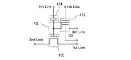
本実施の形態では、半導体装置及び半導体装置の作製方法の一形態を、図1乃至図5を用いて説明する。本実施の形態では、半導体装置の一例として酸化物半導体膜を有するトランジスタを示す。
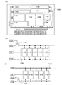
本実施の形態では、本明細書に示すトランジスタを使用した半導体装置の例を図6及び図7を用いて説明する。
本実施の形態では、本明細書に示すトランジスタを使用し、電力が供給されない状況でも記憶内容の保持が可能で、かつ、書き込み回数にも制限が無い半導体装置(記憶装置)の一例を、図面を用いて説明する。
本実施の形態では、半導体装置の一例として、上記実施の形態1に開示したトランジスタを少なくとも一部に用いたCPU(Central Processing Unit)について説明する。
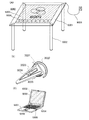
本明細書に開示する半導体装置は、さまざまな電子機器(遊技機も含む)に適用することができる。電子機器としては、テレビ、モニタ等の表示装置、照明装置、デスクトップ型或いはノート型のパーソナルコンピュータ、ワードプロセッサ、DVD(Digital Versatile Disc)などの記録媒体に記憶された静止画又は動画を再生する画像再生装置、ポータブルCDプレーヤ、ラジオ、テープレコーダ、ヘッドホンステレオ、ステレオ、コードレス電話子機、トランシーバ、携帯無線機、携帯電話、自動車電話、携帯型ゲーム機、電卓、携帯情報端末、電子手帳、電子書籍、電子翻訳機、音声入力機器、ビデオカメラ、デジタルスチルカメラ、電気シェーバ、電子レンジ等の高周波加熱装置、電気炊飯器、電気洗濯機、電気掃除機、エアコンディショナーなどの空調設備、食器洗い器、食器乾燥器、衣類乾燥器、布団乾燥器、電気冷蔵庫、電気冷凍庫、電気冷凍冷蔵庫、DNA保存用冷凍庫、煙感知器、放射線測定器、透析装置等の医療機器、などが挙げられる。さらに、誘導灯、信号機、ベルトコンベア、エレベータ、エスカレータ、産業用ロボット、電力貯蔵システム等の産業機器も挙げられる。また、石油を用いたエンジンや、非水系二次電池からの電力を用いて電動機により推進する移動体なども、電気機器の範疇に含まれるものとする。上記移動体として、例えば、電気自動車(EV)、内燃機関と電動機を併せ持ったハイブリッド車(HEV)、プラグインハイブリッド車(PHEV)、これらのタイヤ車輪を無限軌道に変えた装軌車両、電動アシスト自転車を含む原動機付自転車、自動二輪車、電動車椅子、ゴルフ用カート、小型又は大型船舶、潜水艦、ヘリコプター、航空機、ロケット、人工衛星、宇宙探査機や惑星探査機、宇宙船が挙げられる。これらの電子機器の具体例を図11乃至図13に示す。
成膜時基板温度200℃におけるエッチングレート選択比は約30、成膜時基板温度400℃におけるエッチングレート選択比は約20であり、いずれにおいてもエッチングレート選択比20以上という高いエッチングレート選択比が得られたことが確認できた。
Claims (7)
- 第1の電極層を形成し、
前記第1の電極層上に第1の酸化物膜を形成し、
前記第1の酸化物膜上に酸化物半導体膜を形成し、
前記酸化物半導体膜上に第2の酸化物膜を形成し、
前記第2の酸化物膜を線幅方向に後退させながらマスクとして用いて、前記酸化物半導体膜をエッチングし、前記酸化物半導体膜及び前記第2の酸化物膜の柱状体を形成し、
前記柱状体上に絶縁膜を形成し、
前記絶縁膜上に島状の導電膜を形成し、
前記絶縁膜及び前記島状の導電膜を異方性エッチングして、前記柱状体における前記酸化物半導体膜の側面を覆うゲート絶縁膜と、前記ゲート絶縁膜を介して前記柱状体における前記酸化物半導体膜と重なり、かつ対向する第1のゲート電極層及び第2のゲート電極層とを形成し、
前記柱状体における前記第2の酸化物膜に電気的に接続する第2の電極層を形成することを特徴とする半導体装置の作製方法。 - 請求項1において、
前記第1の電極層、前記第1の酸化物膜、前記柱状体、前記ゲート絶縁膜、前記第1のゲート電極層、及び前記第2のゲート電極層上に層間絶縁膜を形成し、
前記層間絶縁膜を選択的に除去して前記柱状体における前記第2の酸化物膜を露出し、
前記露出した第2の酸化物膜と接して前記第2の電極層を形成することを特徴とする半導体装置の作製方法。 - 請求項1又は請求項2において、
前記エッチングは、酢酸、硝酸、及び燐酸の混合液を用い、
前記第1の酸化物膜及び前記第2の酸化物膜は、前記酸化物半導体膜より、酢酸、硝酸、及び燐酸の混合液を用いた前記エッチングに対して耐性があり、該エッチングの速度が遅いことを特徴とする半導体装置の作製方法。 - 請求項1乃至3のいずれか一項において、
前記第1の酸化物膜及び前記第2の酸化物膜は、前記酸化物半導体膜より低抵抗であり、
前記酸化物半導体膜はチャネル形成領域として機能し、
前記第1の酸化物膜及び前記第2の酸化物膜は、ソース領域又はドレイン領域として機能することを特徴とする半導体装置の作製方法。 - 請求項1乃至4のいずれか一項において、
前記エッチングする前に、前記酸化物半導体膜及び前記第2の酸化物膜上にレジストマスクを形成し、前記レジストマスクを用いた異方性エッチングにより前記酸化物半導体膜、及び前記第2の酸化物膜を島状に加工することを特徴とする半導体装置の作製方法。 - 請求項1乃至5のいずれか一項において、
前記第2の酸化物膜は、インジウム、ガリウム、亜鉛、及び窒素を主成分として含むターゲットを用いたスパッタリング法により形成することを特徴とする半導体装置の作製方法。 - 請求項1乃至5のいずれか一項において、
前記第2の酸化物膜は、インジウム、ガリウム、亜鉛を主成分として含む酸化物膜を形成し、該酸化物膜に窒素を導入して形成することを特徴とする半導体装置の作製方法。
Priority Applications (1)
| Application Number | Priority Date | Filing Date | Title |
|---|---|---|---|
| JP2013089149A JP6100071B2 (ja) | 2012-04-30 | 2013-04-22 | 半導体装置の作製方法 |
Applications Claiming Priority (3)
| Application Number | Priority Date | Filing Date | Title |
|---|---|---|---|
| JP2012104279 | 2012-04-30 | ||
| JP2012104279 | 2012-04-30 | ||
| JP2013089149A JP6100071B2 (ja) | 2012-04-30 | 2013-04-22 | 半導体装置の作製方法 |
Publications (3)
| Publication Number | Publication Date |
|---|---|
| JP2013251533A JP2013251533A (ja) | 2013-12-12 |
| JP2013251533A5 JP2013251533A5 (ja) | 2016-05-19 |
| JP6100071B2 true JP6100071B2 (ja) | 2017-03-22 |
Family
ID=49476514
Family Applications (1)
| Application Number | Title | Priority Date | Filing Date |
|---|---|---|---|
| JP2013089149A Expired - Fee Related JP6100071B2 (ja) | 2012-04-30 | 2013-04-22 | 半導体装置の作製方法 |
Country Status (2)
| Country | Link |
|---|---|
| US (1) | US8772771B2 (ja) |
| JP (1) | JP6100071B2 (ja) |
Cited By (1)
| Publication number | Priority date | Publication date | Assignee | Title |
|---|---|---|---|---|
| US11074944B2 (en) | 2018-10-31 | 2021-07-27 | Toshiba Memory Corporation | Semiconductor memory device |
Families Citing this family (28)
| Publication number | Priority date | Publication date | Assignee | Title |
|---|---|---|---|---|
| US9368619B2 (en) | 2013-02-08 | 2016-06-14 | Taiwan Semiconductor Manufacturing Company, Ltd. | Method for inducing strain in vertical semiconductor columns |
| US9466668B2 (en) | 2013-02-08 | 2016-10-11 | Taiwan Semiconductor Manufacturing Company, Ltd. | Inducing localized strain in vertical nanowire transistors |
| US9209247B2 (en) * | 2013-05-10 | 2015-12-08 | Taiwan Semiconductor Manufacturing Company, Ltd. | Self-aligned wrapped-around structure |
| US9978863B2 (en) * | 2013-08-16 | 2018-05-22 | Taiwan Semiconductor Manufacturing Company Limited | Semiconductor arrangement with one or more semiconductor columns |
| JP6347704B2 (ja) | 2013-09-18 | 2018-06-27 | 株式会社半導体エネルギー研究所 | 半導体装置 |
| KR20160087024A (ko) | 2015-01-12 | 2016-07-21 | 삼성디스플레이 주식회사 | 박막트랜지스터 및 그의 제조방법 |
| US9564493B2 (en) | 2015-03-13 | 2017-02-07 | Taiwan Semiconductor Manufacturing Company, Ltd. | Devices having a semiconductor material that is semimetal in bulk and methods of forming the same |
| US10141232B2 (en) | 2016-06-30 | 2018-11-27 | International Business Machines Corporation | Vertical CMOS devices with common gate stacks |
| US10014305B2 (en) | 2016-11-01 | 2018-07-03 | Micron Technology, Inc. | Methods of forming an array comprising pairs of vertically opposed capacitors and arrays comprising pairs of vertically opposed capacitors |
| US10062745B2 (en) | 2017-01-09 | 2018-08-28 | Micron Technology, Inc. | Methods of forming an array of capacitors, methods of forming an array of memory cells individually comprising a capacitor and a transistor, arrays of capacitors, and arrays of memory cells individually comprising a capacitor and a transistor |
| US9935114B1 (en) | 2017-01-10 | 2018-04-03 | Micron Technology, Inc. | Methods of forming an array comprising pairs of vertically opposed capacitors and arrays comprising pairs of vertically opposed capacitors |
| US9842839B1 (en) * | 2017-01-12 | 2017-12-12 | Micron Technology, Inc. | Memory cell, an array of memory cells individually comprising a capacitor and a transistor with the array comprising rows of access lines and columns of digit lines, a 2T-1C memory cell, and methods of forming an array of capacitors and access transistors there-above |
| TWI648825B (zh) * | 2017-03-16 | 2019-01-21 | 日商東芝記憶體股份有限公司 | 半導體記憶體 |
| US10312239B2 (en) | 2017-03-16 | 2019-06-04 | Toshiba Memory Corporation | Semiconductor memory including semiconductor oxie |
| US10553601B2 (en) | 2017-03-16 | 2020-02-04 | Toshiba Memory Corporation | Semiconductor memory including semiconductor oxide |
| US10497712B2 (en) | 2017-03-16 | 2019-12-03 | Toshiba Memory Corporation | Semiconductor memory |
| WO2018236359A1 (en) * | 2017-06-20 | 2018-12-27 | Intel Corporation | Thin film core-shell fin and nanowire transistors |
| JP7109928B2 (ja) | 2018-01-31 | 2022-08-01 | キオクシア株式会社 | トランジスタ及び半導体記憶装置並びにトランジスタの製造方法 |
| US10388658B1 (en) | 2018-04-27 | 2019-08-20 | Micron Technology, Inc. | Transistors, arrays of transistors, arrays of memory cells individually comprising a capacitor and an elevationally-extending transistor, and methods of forming an array of transistors |
| WO2020076766A1 (en) | 2018-10-09 | 2020-04-16 | Micron Technology, Inc. | Methods of forming a device, and related devices and electronic systems |
| KR20210053353A (ko) * | 2018-10-09 | 2021-05-11 | 마이크론 테크놀로지, 인크 | 수소 배리어 재료를 갖는 종형 트랜지스터를 포함하는 디바이스, 및 관련 방법 |
| WO2020076851A1 (en) | 2018-10-09 | 2020-04-16 | Micron Technology, Inc. | Devices and electronic systems including vertical transistors, and related methods |
| JP2021150525A (ja) | 2020-03-19 | 2021-09-27 | キオクシア株式会社 | 半導体記憶装置及び半導体記憶装置の製造方法 |
| CN111599870A (zh) | 2020-05-29 | 2020-08-28 | 京东方科技集团股份有限公司 | 一种薄膜晶体管开关及其制备方法、阵列基板和显示面板 |
| US11430895B2 (en) * | 2020-06-03 | 2022-08-30 | Micron Technology, Inc. | Transistors including oxide semiconductive materials, and related microelectronic devices, memory devices, electronic systems, and methods |
| US12575132B2 (en) | 2022-04-15 | 2026-03-10 | Semiconductor Energy Laboratory Co., Ltd. | Semiconductor device |
| CN121464736A (zh) * | 2023-05-12 | 2026-02-03 | 株式会社半导体能源研究所 | 半导体装置、存储装置、半导体装置的制造方法 |
| CN121713685A (zh) * | 2023-08-24 | 2026-03-20 | 东京毅力科创株式会社 | 基板处理方法和基板处理装置 |
Family Cites Families (107)
| Publication number | Priority date | Publication date | Assignee | Title |
|---|---|---|---|---|
| JPH11505377A (ja) | 1995-08-03 | 1999-05-18 | フィリップス エレクトロニクス ネムローゼ フェンノートシャップ | 半導体装置 |
| JP3625598B2 (ja) | 1995-12-30 | 2005-03-02 | 三星電子株式会社 | 液晶表示装置の製造方法 |
| JP4170454B2 (ja) | 1998-07-24 | 2008-10-22 | Hoya株式会社 | 透明導電性酸化物薄膜を有する物品及びその製造方法 |
| JP2000150861A (ja) | 1998-11-16 | 2000-05-30 | Tdk Corp | 酸化物薄膜 |
| JP3276930B2 (ja) | 1998-11-17 | 2002-04-22 | 科学技術振興事業団 | トランジスタ及び半導体装置 |
| TW460731B (en) | 1999-09-03 | 2001-10-21 | Ind Tech Res Inst | Electrode structure and production method of wide viewing angle LCD |
| JP4089858B2 (ja) | 2000-09-01 | 2008-05-28 | 国立大学法人東北大学 | 半導体デバイス |
| KR20020038482A (ko) | 2000-11-15 | 2002-05-23 | 모리시타 요이찌 | 박막 트랜지스터 어레이, 그 제조방법 및 그것을 이용한표시패널 |
| US6531727B2 (en) * | 2001-02-09 | 2003-03-11 | Micron Technology, Inc. | Open bit line DRAM with ultra thin body transistors |
| JP3997731B2 (ja) | 2001-03-19 | 2007-10-24 | 富士ゼロックス株式会社 | 基材上に結晶性半導体薄膜を形成する方法 |
| JP2002289859A (ja) | 2001-03-23 | 2002-10-04 | Minolta Co Ltd | 薄膜トランジスタ |
| JP4090716B2 (ja) | 2001-09-10 | 2008-05-28 | 雅司 川崎 | 薄膜トランジスタおよびマトリクス表示装置 |
| JP3925839B2 (ja) | 2001-09-10 | 2007-06-06 | シャープ株式会社 | 半導体記憶装置およびその試験方法 |
| JP2003101012A (ja) | 2001-09-25 | 2003-04-04 | Sony Corp | 半導体装置およびその製造方法 |
| EP1443130B1 (en) | 2001-11-05 | 2011-09-28 | Japan Science and Technology Agency | Natural superlattice homologous single crystal thin film, method for preparation thereof, and device using said single crystal thin film |
| JP4164562B2 (ja) | 2002-09-11 | 2008-10-15 | 独立行政法人科学技術振興機構 | ホモロガス薄膜を活性層として用いる透明薄膜電界効果型トランジスタ |
| JP4083486B2 (ja) | 2002-02-21 | 2008-04-30 | 独立行政法人科学技術振興機構 | LnCuO(S,Se,Te)単結晶薄膜の製造方法 |
| US7049190B2 (en) | 2002-03-15 | 2006-05-23 | Sanyo Electric Co., Ltd. | Method for forming ZnO film, method for forming ZnO semiconductor layer, method for fabricating semiconductor device, and semiconductor device |
| JP3933591B2 (ja) | 2002-03-26 | 2007-06-20 | 淳二 城戸 | 有機エレクトロルミネッセント素子 |
| US7339187B2 (en) | 2002-05-21 | 2008-03-04 | State Of Oregon Acting By And Through The Oregon State Board Of Higher Education On Behalf Of Oregon State University | Transistor structures |
| JP2004022625A (ja) | 2002-06-13 | 2004-01-22 | Murata Mfg Co Ltd | 半導体デバイス及び該半導体デバイスの製造方法 |
| US7105868B2 (en) | 2002-06-24 | 2006-09-12 | Cermet, Inc. | High-electron mobility transistor with zinc oxide |
| JP4355807B2 (ja) * | 2002-08-28 | 2009-11-04 | 独立行政法人産業技術総合研究所 | 二重ゲート型mos電界効果トランジスタ及びその作製方法 |
| US6632712B1 (en) * | 2002-10-03 | 2003-10-14 | Chartered Semiconductor Manufacturing Ltd. | Method of fabricating variable length vertical transistors |
| US7067843B2 (en) | 2002-10-11 | 2006-06-27 | E. I. Du Pont De Nemours And Company | Transparent oxide semiconductor thin film transistors |
| US7138685B2 (en) * | 2002-12-11 | 2006-11-21 | International Business Machines Corporation | Vertical MOSFET SRAM cell |
| JP4166105B2 (ja) | 2003-03-06 | 2008-10-15 | シャープ株式会社 | 半導体装置およびその製造方法 |
| JP2004273732A (ja) | 2003-03-07 | 2004-09-30 | Sharp Corp | アクティブマトリクス基板およびその製造方法 |
| JP4108633B2 (ja) | 2003-06-20 | 2008-06-25 | シャープ株式会社 | 薄膜トランジスタおよびその製造方法ならびに電子デバイス |
| US7262463B2 (en) | 2003-07-25 | 2007-08-28 | Hewlett-Packard Development Company, L.P. | Transistor including a deposited channel region having a doped portion |
| EP1737044B1 (en) | 2004-03-12 | 2014-12-10 | Japan Science and Technology Agency | Amorphous oxide and thin film transistor |
| US7282782B2 (en) | 2004-03-12 | 2007-10-16 | Hewlett-Packard Development Company, L.P. | Combined binary oxide semiconductor device |
| US7297977B2 (en) | 2004-03-12 | 2007-11-20 | Hewlett-Packard Development Company, L.P. | Semiconductor device |
| US7145174B2 (en) | 2004-03-12 | 2006-12-05 | Hewlett-Packard Development Company, Lp. | Semiconductor device |
| US7211825B2 (en) | 2004-06-14 | 2007-05-01 | Yi-Chi Shih | Indium oxide-based thin film transistors and circuits |
| JP2006100760A (ja) | 2004-09-02 | 2006-04-13 | Casio Comput Co Ltd | 薄膜トランジスタおよびその製造方法 |
| US7285501B2 (en) | 2004-09-17 | 2007-10-23 | Hewlett-Packard Development Company, L.P. | Method of forming a solution processed device |
| US7298084B2 (en) | 2004-11-02 | 2007-11-20 | 3M Innovative Properties Company | Methods and displays utilizing integrated zinc oxide row and column drivers in conjunction with organic light emitting diodes |
| US7453065B2 (en) | 2004-11-10 | 2008-11-18 | Canon Kabushiki Kaisha | Sensor and image pickup device |
| US7829444B2 (en) | 2004-11-10 | 2010-11-09 | Canon Kabushiki Kaisha | Field effect transistor manufacturing method |
| RU2358354C2 (ru) | 2004-11-10 | 2009-06-10 | Кэнон Кабусики Кайся | Светоизлучающее устройство |
| KR100998527B1 (ko) | 2004-11-10 | 2010-12-07 | 고쿠리츠다이가쿠호진 토쿄고교 다이가꾸 | 비정질 산화물 및 전계 효과 트랜지스터 |
| EP1815530B1 (en) | 2004-11-10 | 2021-02-17 | Canon Kabushiki Kaisha | Field effect transistor employing an amorphous oxide |
| US7863611B2 (en) | 2004-11-10 | 2011-01-04 | Canon Kabushiki Kaisha | Integrated circuits utilizing amorphous oxides |
| US7791072B2 (en) | 2004-11-10 | 2010-09-07 | Canon Kabushiki Kaisha | Display |
| US7579224B2 (en) | 2005-01-21 | 2009-08-25 | Semiconductor Energy Laboratory Co., Ltd. | Method for manufacturing a thin film semiconductor device |
| TWI505473B (zh) | 2005-01-28 | 2015-10-21 | 半導體能源研究所股份有限公司 | 半導體裝置,電子裝置,和半導體裝置的製造方法 |
| TWI481024B (zh) | 2005-01-28 | 2015-04-11 | 半導體能源研究所股份有限公司 | 半導體裝置,電子裝置,和半導體裝置的製造方法 |
| US7858451B2 (en) | 2005-02-03 | 2010-12-28 | Semiconductor Energy Laboratory Co., Ltd. | Electronic device, semiconductor device and manufacturing method thereof |
| US7948171B2 (en) | 2005-02-18 | 2011-05-24 | Semiconductor Energy Laboratory Co., Ltd. | Light emitting device |
| US20060197092A1 (en) | 2005-03-03 | 2006-09-07 | Randy Hoffman | System and method for forming conductive material on a substrate |
| US8681077B2 (en) | 2005-03-18 | 2014-03-25 | Semiconductor Energy Laboratory Co., Ltd. | Semiconductor device, and display device, driving method and electronic apparatus thereof |
| US7544967B2 (en) | 2005-03-28 | 2009-06-09 | Massachusetts Institute Of Technology | Low voltage flexible organic/transparent transistor for selective gas sensing, photodetecting and CMOS device applications |
| US7645478B2 (en) | 2005-03-31 | 2010-01-12 | 3M Innovative Properties Company | Methods of making displays |
| US8300031B2 (en) | 2005-04-20 | 2012-10-30 | Semiconductor Energy Laboratory Co., Ltd. | Semiconductor device comprising transistor having gate and drain connected through a current-voltage conversion element |
| JP2006344849A (ja) | 2005-06-10 | 2006-12-21 | Casio Comput Co Ltd | 薄膜トランジスタ |
| US7691666B2 (en) | 2005-06-16 | 2010-04-06 | Eastman Kodak Company | Methods of making thin film transistors comprising zinc-oxide-based semiconductor materials and transistors made thereby |
| US7402506B2 (en) | 2005-06-16 | 2008-07-22 | Eastman Kodak Company | Methods of making thin film transistors comprising zinc-oxide-based semiconductor materials and transistors made thereby |
| US7507618B2 (en) | 2005-06-27 | 2009-03-24 | 3M Innovative Properties Company | Method for making electronic devices using metal oxide nanoparticles |
| KR100711890B1 (ko) | 2005-07-28 | 2007-04-25 | 삼성에스디아이 주식회사 | 유기 발광표시장치 및 그의 제조방법 |
| JP2007059128A (ja) | 2005-08-23 | 2007-03-08 | Canon Inc | 有機el表示装置およびその製造方法 |
| JP4850457B2 (ja) | 2005-09-06 | 2012-01-11 | キヤノン株式会社 | 薄膜トランジスタ及び薄膜ダイオード |
| JP5116225B2 (ja) | 2005-09-06 | 2013-01-09 | キヤノン株式会社 | 酸化物半導体デバイスの製造方法 |
| JP2007073705A (ja) | 2005-09-06 | 2007-03-22 | Canon Inc | 酸化物半導体チャネル薄膜トランジスタおよびその製造方法 |
| JP4280736B2 (ja) | 2005-09-06 | 2009-06-17 | キヤノン株式会社 | 半導体素子 |
| EP1998373A3 (en) | 2005-09-29 | 2012-10-31 | Semiconductor Energy Laboratory Co, Ltd. | Semiconductor device having oxide semiconductor layer and manufacturing method thereof |
| JP5037808B2 (ja) | 2005-10-20 | 2012-10-03 | キヤノン株式会社 | アモルファス酸化物を用いた電界効果型トランジスタ、及び該トランジスタを用いた表示装置 |
| CN101577231B (zh) | 2005-11-15 | 2013-01-02 | 株式会社半导体能源研究所 | 半导体器件及其制造方法 |
| TWI292281B (en) | 2005-12-29 | 2008-01-01 | Ind Tech Res Inst | Pixel structure of active organic light emitting diode and method of fabricating the same |
| US7867636B2 (en) | 2006-01-11 | 2011-01-11 | Murata Manufacturing Co., Ltd. | Transparent conductive film and method for manufacturing the same |
| JP4977478B2 (ja) | 2006-01-21 | 2012-07-18 | 三星電子株式会社 | ZnOフィルム及びこれを用いたTFTの製造方法 |
| US7576394B2 (en) | 2006-02-02 | 2009-08-18 | Kochi Industrial Promotion Center | Thin film transistor including low resistance conductive thin films and manufacturing method thereof |
| US7977169B2 (en) | 2006-02-15 | 2011-07-12 | Kochi Industrial Promotion Center | Semiconductor device including active layer made of zinc oxide with controlled orientations and manufacturing method thereof |
| US7977736B2 (en) * | 2006-02-23 | 2011-07-12 | Samsung Electronics Co., Ltd. | Vertical channel transistors and memory devices including vertical channel transistors |
| KR20070101595A (ko) | 2006-04-11 | 2007-10-17 | 삼성전자주식회사 | ZnO TFT |
| US20070252928A1 (en) | 2006-04-28 | 2007-11-01 | Toppan Printing Co., Ltd. | Structure, transmission type liquid crystal display, reflection type display and manufacturing method thereof |
| JP5028033B2 (ja) | 2006-06-13 | 2012-09-19 | キヤノン株式会社 | 酸化物半導体膜のドライエッチング方法 |
| JP4609797B2 (ja) | 2006-08-09 | 2011-01-12 | Nec液晶テクノロジー株式会社 | 薄膜デバイス及びその製造方法 |
| JP4999400B2 (ja) | 2006-08-09 | 2012-08-15 | キヤノン株式会社 | 酸化物半導体膜のドライエッチング方法 |
| JP4332545B2 (ja) | 2006-09-15 | 2009-09-16 | キヤノン株式会社 | 電界効果型トランジスタ及びその製造方法 |
| JP4274219B2 (ja) | 2006-09-27 | 2009-06-03 | セイコーエプソン株式会社 | 電子デバイス、有機エレクトロルミネッセンス装置、有機薄膜半導体装置 |
| JP5164357B2 (ja) | 2006-09-27 | 2013-03-21 | キヤノン株式会社 | 半導体装置及び半導体装置の製造方法 |
| US7622371B2 (en) | 2006-10-10 | 2009-11-24 | Hewlett-Packard Development Company, L.P. | Fused nanocrystal thin film semiconductor and method |
| US7772021B2 (en) | 2006-11-29 | 2010-08-10 | Samsung Electronics Co., Ltd. | Flat panel displays comprising a thin-film transistor having a semiconductive oxide in its channel and methods of fabricating the same for use in flat panel displays |
| JP2008140684A (ja) | 2006-12-04 | 2008-06-19 | Toppan Printing Co Ltd | カラーelディスプレイおよびその製造方法 |
| KR101303578B1 (ko) | 2007-01-05 | 2013-09-09 | 삼성전자주식회사 | 박막 식각 방법 |
| US8207063B2 (en) | 2007-01-26 | 2012-06-26 | Eastman Kodak Company | Process for atomic layer deposition |
| KR100851215B1 (ko) | 2007-03-14 | 2008-08-07 | 삼성에스디아이 주식회사 | 박막 트랜지스터 및 이를 이용한 유기 전계 발광표시장치 |
| US7795613B2 (en) | 2007-04-17 | 2010-09-14 | Toppan Printing Co., Ltd. | Structure with transistor |
| KR101325053B1 (ko) | 2007-04-18 | 2013-11-05 | 삼성디스플레이 주식회사 | 박막 트랜지스터 기판 및 이의 제조 방법 |
| KR20080094300A (ko) | 2007-04-19 | 2008-10-23 | 삼성전자주식회사 | 박막 트랜지스터 및 그 제조 방법과 박막 트랜지스터를포함하는 평판 디스플레이 |
| KR101334181B1 (ko) | 2007-04-20 | 2013-11-28 | 삼성전자주식회사 | 선택적으로 결정화된 채널층을 갖는 박막 트랜지스터 및 그제조 방법 |
| WO2008133345A1 (en) | 2007-04-25 | 2008-11-06 | Canon Kabushiki Kaisha | Oxynitride semiconductor |
| KR101345376B1 (ko) | 2007-05-29 | 2013-12-24 | 삼성전자주식회사 | ZnO 계 박막 트랜지스터 및 그 제조방법 |
| JP5377940B2 (ja) * | 2007-12-03 | 2013-12-25 | 株式会社半導体エネルギー研究所 | 半導体装置 |
| US8202365B2 (en) | 2007-12-17 | 2012-06-19 | Fujifilm Corporation | Process for producing oriented inorganic crystalline film, and semiconductor device using the oriented inorganic crystalline film |
| JP4623179B2 (ja) | 2008-09-18 | 2011-02-02 | ソニー株式会社 | 薄膜トランジスタおよびその製造方法 |
| JP5430113B2 (ja) * | 2008-10-08 | 2014-02-26 | キヤノン株式会社 | 電界効果型トランジスタ及びその製造方法 |
| JP5451280B2 (ja) | 2008-10-09 | 2014-03-26 | キヤノン株式会社 | ウルツ鉱型結晶成長用基板およびその製造方法ならびに半導体装置 |
| TWI535037B (zh) * | 2008-11-07 | 2016-05-21 | 半導體能源研究所股份有限公司 | 半導體裝置和其製造方法 |
| JP5525156B2 (ja) * | 2008-12-09 | 2014-06-18 | ピーエスフォー ルクスコ エスエイアールエル | 半導体装置、および該半導体装置の製造方法 |
| WO2011052411A1 (en) | 2009-10-30 | 2011-05-05 | Semiconductor Energy Laboratory Co., Ltd. | Transistor |
| KR101800854B1 (ko) * | 2009-11-20 | 2017-11-23 | 가부시키가이샤 한도오따이 에네루기 켄큐쇼 | 트랜지스터 |
| JP5520084B2 (ja) | 2010-03-03 | 2014-06-11 | 富士フイルム株式会社 | 電界効果型トランジスタの製造方法 |
| TWI508294B (zh) * | 2010-08-19 | 2015-11-11 | 半導體能源研究所股份有限公司 | 半導體裝置 |
| JP2012182354A (ja) * | 2011-03-02 | 2012-09-20 | Toshiba Corp | 半導体記憶装置 |
| US8723281B2 (en) * | 2011-03-23 | 2014-05-13 | Avalanche Technology Inc. | Access transistor with a buried gate |
-
2013
- 2013-04-22 JP JP2013089149A patent/JP6100071B2/ja not_active Expired - Fee Related
- 2013-04-25 US US13/870,370 patent/US8772771B2/en not_active Expired - Fee Related
Cited By (1)
| Publication number | Priority date | Publication date | Assignee | Title |
|---|---|---|---|---|
| US11074944B2 (en) | 2018-10-31 | 2021-07-27 | Toshiba Memory Corporation | Semiconductor memory device |
Also Published As
| Publication number | Publication date |
|---|---|
| JP2013251533A (ja) | 2013-12-12 |
| US20130285051A1 (en) | 2013-10-31 |
| US8772771B2 (en) | 2014-07-08 |
Similar Documents
| Publication | Publication Date | Title |
|---|---|---|
| JP6100071B2 (ja) | 半導体装置の作製方法 | |
| JP7113879B2 (ja) | 半導体装置 | |
| JP6574861B2 (ja) | 半導体装置 | |
| JP6416981B2 (ja) | 半導体装置 | |
| JP6366800B2 (ja) | 半導体装置及び半導体装置の製造方法 | |
| JP6499246B2 (ja) | 半導体装置 | |
| JP6419911B2 (ja) | 半導体装置 | |
| US9219164B2 (en) | Semiconductor device with oxide semiconductor channel | |
| JP6230808B2 (ja) | 半導体装置 | |
| JP6186166B2 (ja) | 半導体装置 | |
| JP6293818B2 (ja) | 半導体装置の作製方法 | |
| JP2018121061A (ja) | 半導体装置 |
Legal Events
| Date | Code | Title | Description |
|---|---|---|---|
| A521 | Request for written amendment filed |
Free format text: JAPANESE INTERMEDIATE CODE: A523 Effective date: 20160328 |
|
| A621 | Written request for application examination |
Free format text: JAPANESE INTERMEDIATE CODE: A621 Effective date: 20160328 |
|
| A977 | Report on retrieval |
Free format text: JAPANESE INTERMEDIATE CODE: A971007 Effective date: 20170131 |
|
| TRDD | Decision of grant or rejection written | ||
| A01 | Written decision to grant a patent or to grant a registration (utility model) |
Free format text: JAPANESE INTERMEDIATE CODE: A01 Effective date: 20170214 |
|
| A61 | First payment of annual fees (during grant procedure) |
Free format text: JAPANESE INTERMEDIATE CODE: A61 Effective date: 20170222 |
|
| R150 | Certificate of patent or registration of utility model |
Ref document number: 6100071 Country of ref document: JP Free format text: JAPANESE INTERMEDIATE CODE: R150 |
|
| R250 | Receipt of annual fees |
Free format text: JAPANESE INTERMEDIATE CODE: R250 |
|
| LAPS | Cancellation because of no payment of annual fees |