JP6052182B2 - Organic electroluminescence device and planar light emitter - Google Patents
Organic electroluminescence device and planar light emitter Download PDFInfo
- Publication number
- JP6052182B2 JP6052182B2 JP2013544176A JP2013544176A JP6052182B2 JP 6052182 B2 JP6052182 B2 JP 6052182B2 JP 2013544176 A JP2013544176 A JP 2013544176A JP 2013544176 A JP2013544176 A JP 2013544176A JP 6052182 B2 JP6052182 B2 JP 6052182B2
- Authority
- JP
- Japan
- Prior art keywords
- organic
- light
- light extraction
- layer
- film
- Prior art date
- Legal status (The legal status is an assumption and is not a legal conclusion. Google has not performed a legal analysis and makes no representation as to the accuracy of the status listed.)
- Expired - Fee Related
Links
- 238000005401 electroluminescence Methods 0.000 title claims description 16
- 238000000605 extraction Methods 0.000 claims description 166
- 239000000463 material Substances 0.000 claims description 165
- 239000000758 substrate Substances 0.000 claims description 120
- 239000010408 film Substances 0.000 claims description 111
- 150000001875 compounds Chemical class 0.000 claims description 72
- -1 polyethylene terephthalate Polymers 0.000 claims description 52
- 229910052751 metal Inorganic materials 0.000 claims description 35
- 239000002184 metal Substances 0.000 claims description 35
- 150000002894 organic compounds Chemical class 0.000 claims description 31
- 229920000139 polyethylene terephthalate Polymers 0.000 claims description 22
- 239000005020 polyethylene terephthalate Substances 0.000 claims description 22
- 238000002834 transmittance Methods 0.000 claims description 20
- 239000011521 glass Substances 0.000 claims description 18
- 239000011888 foil Substances 0.000 claims description 15
- 229920001721 polyimide Polymers 0.000 claims description 15
- 239000010409 thin film Substances 0.000 claims description 12
- WKBOTKDWSSQWDR-UHFFFAOYSA-N Bromine atom Chemical compound [Br] WKBOTKDWSSQWDR-UHFFFAOYSA-N 0.000 claims description 11
- 150000003377 silicon compounds Chemical class 0.000 claims description 11
- GDTBXPJZTBHREO-UHFFFAOYSA-N bromine Substances BrBr GDTBXPJZTBHREO-UHFFFAOYSA-N 0.000 claims description 10
- 229910052794 bromium Inorganic materials 0.000 claims description 10
- 229920006289 polycarbonate film Polymers 0.000 claims description 5
- 239000004925 Acrylic resin Substances 0.000 claims description 2
- 229920006290 polyethylene naphthalate film Polymers 0.000 claims description 2
- 238000004020 luminiscence type Methods 0.000 claims 1
- 239000010410 layer Substances 0.000 description 379
- 238000000034 method Methods 0.000 description 113
- 230000032258 transport Effects 0.000 description 68
- 230000005525 hole transport Effects 0.000 description 53
- 238000002347 injection Methods 0.000 description 50
- 239000007924 injection Substances 0.000 description 50
- 239000000243 solution Substances 0.000 description 37
- 239000011347 resin Substances 0.000 description 33
- 229920005989 resin Polymers 0.000 description 33
- 239000000203 mixture Substances 0.000 description 31
- 230000000903 blocking effect Effects 0.000 description 30
- 238000000576 coating method Methods 0.000 description 28
- 238000011156 evaluation Methods 0.000 description 28
- 239000011248 coating agent Substances 0.000 description 27
- 239000002245 particle Substances 0.000 description 27
- 239000000853 adhesive Substances 0.000 description 24
- 230000001070 adhesive effect Effects 0.000 description 24
- 230000000052 comparative effect Effects 0.000 description 23
- 238000009792 diffusion process Methods 0.000 description 23
- 239000002585 base Substances 0.000 description 19
- VYPSYNLAJGMNEJ-UHFFFAOYSA-N silicon dioxide Inorganic materials O=[Si]=O VYPSYNLAJGMNEJ-UHFFFAOYSA-N 0.000 description 19
- 229910052782 aluminium Inorganic materials 0.000 description 15
- XAGFODPZIPBFFR-UHFFFAOYSA-N aluminium Chemical compound [Al] XAGFODPZIPBFFR-UHFFFAOYSA-N 0.000 description 15
- 239000000872 buffer Substances 0.000 description 15
- 239000007787 solid Substances 0.000 description 15
- 239000000126 substance Substances 0.000 description 14
- 239000007772 electrode material Substances 0.000 description 13
- 229910052757 nitrogen Inorganic materials 0.000 description 13
- 238000007789 sealing Methods 0.000 description 13
- 239000003566 sealing material Substances 0.000 description 13
- 230000004888 barrier function Effects 0.000 description 12
- 239000000975 dye Substances 0.000 description 12
- 238000004519 manufacturing process Methods 0.000 description 11
- 238000007740 vapor deposition Methods 0.000 description 11
- 238000004383 yellowing Methods 0.000 description 11
- 239000002861 polymer material Substances 0.000 description 10
- 230000008569 process Effects 0.000 description 10
- DKPFZGUDAPQIHT-UHFFFAOYSA-N Butyl acetate Natural products CCCCOC(C)=O DKPFZGUDAPQIHT-UHFFFAOYSA-N 0.000 description 8
- FYYHWMGAXLPEAU-UHFFFAOYSA-N Magnesium Chemical compound [Mg] FYYHWMGAXLPEAU-UHFFFAOYSA-N 0.000 description 8
- 238000010438 heat treatment Methods 0.000 description 8
- FUZZWVXGSFPDMH-UHFFFAOYSA-M hexanoate Chemical compound CCCCCC([O-])=O FUZZWVXGSFPDMH-UHFFFAOYSA-M 0.000 description 8
- 229910010272 inorganic material Inorganic materials 0.000 description 8
- 239000012948 isocyanate Substances 0.000 description 8
- 239000011777 magnesium Substances 0.000 description 8
- 229910052749 magnesium Inorganic materials 0.000 description 8
- NROKBHXJSPEDAR-UHFFFAOYSA-M potassium fluoride Chemical compound [F-].[K+] NROKBHXJSPEDAR-UHFFFAOYSA-M 0.000 description 8
- 239000000377 silicon dioxide Substances 0.000 description 8
- XLYOFNOQVPJJNP-UHFFFAOYSA-N water Chemical compound O XLYOFNOQVPJJNP-UHFFFAOYSA-N 0.000 description 8
- RTTZISZSHSCFRH-UHFFFAOYSA-N 1,3-bis(isocyanatomethyl)benzene Chemical compound O=C=NCC1=CC=CC(CN=C=O)=C1 RTTZISZSHSCFRH-UHFFFAOYSA-N 0.000 description 7
- 239000004642 Polyimide Substances 0.000 description 7
- 230000015572 biosynthetic process Effects 0.000 description 7
- 229920001577 copolymer Polymers 0.000 description 7
- 150000002513 isocyanates Chemical class 0.000 description 7
- 239000011368 organic material Substances 0.000 description 7
- 230000035699 permeability Effects 0.000 description 7
- 239000011112 polyethylene naphthalate Substances 0.000 description 7
- 229920000642 polymer Polymers 0.000 description 7
- 229920005862 polyol Polymers 0.000 description 7
- 238000006862 quantum yield reaction Methods 0.000 description 7
- 239000012780 transparent material Substances 0.000 description 7
- 239000000654 additive Substances 0.000 description 6
- 230000000996 additive effect Effects 0.000 description 6
- QVGXLLKOCUKJST-UHFFFAOYSA-N atomic oxygen Chemical compound [O] QVGXLLKOCUKJST-UHFFFAOYSA-N 0.000 description 6
- 239000011147 inorganic material Substances 0.000 description 6
- 239000007788 liquid Substances 0.000 description 6
- 150000004767 nitrides Chemical class 0.000 description 6
- 239000001301 oxygen Substances 0.000 description 6
- 229910052760 oxygen Inorganic materials 0.000 description 6
- 229920003229 poly(methyl methacrylate) Polymers 0.000 description 6
- 239000004926 polymethyl methacrylate Substances 0.000 description 6
- 229910052710 silicon Inorganic materials 0.000 description 6
- 238000004544 sputter deposition Methods 0.000 description 6
- VZSRBBMJRBPUNF-UHFFFAOYSA-N 2-(2,3-dihydro-1H-inden-2-ylamino)-N-[3-oxo-3-(2,4,6,7-tetrahydrotriazolo[4,5-c]pyridin-5-yl)propyl]pyrimidine-5-carboxamide Chemical compound C1C(CC2=CC=CC=C12)NC1=NC=C(C=N1)C(=O)NCCC(N1CC2=C(CC1)NN=N2)=O VZSRBBMJRBPUNF-UHFFFAOYSA-N 0.000 description 5
- XLOMVQKBTHCTTD-UHFFFAOYSA-N Zinc monoxide Chemical compound [Zn]=O XLOMVQKBTHCTTD-UHFFFAOYSA-N 0.000 description 5
- 229910044991 metal oxide Inorganic materials 0.000 description 5
- 150000004706 metal oxides Chemical class 0.000 description 5
- 239000012044 organic layer Substances 0.000 description 5
- 229920003207 poly(ethylene-2,6-naphthalate) Polymers 0.000 description 5
- 238000012360 testing method Methods 0.000 description 5
- 238000001771 vacuum deposition Methods 0.000 description 5
- VVQNEPGJFQJSBK-UHFFFAOYSA-N Methyl methacrylate Chemical group COC(=O)C(C)=C VVQNEPGJFQJSBK-UHFFFAOYSA-N 0.000 description 4
- 239000004793 Polystyrene Substances 0.000 description 4
- XUIMIQQOPSSXEZ-UHFFFAOYSA-N Silicon Chemical compound [Si] XUIMIQQOPSSXEZ-UHFFFAOYSA-N 0.000 description 4
- 150000001716 carbazoles Chemical class 0.000 description 4
- 239000000969 carrier Substances 0.000 description 4
- 238000010586 diagram Methods 0.000 description 4
- 230000000694 effects Effects 0.000 description 4
- 230000005281 excited state Effects 0.000 description 4
- 230000009477 glass transition Effects 0.000 description 4
- 229910052738 indium Inorganic materials 0.000 description 4
- 239000000178 monomer Substances 0.000 description 4
- 230000003287 optical effect Effects 0.000 description 4
- TWNQGVIAIRXVLR-UHFFFAOYSA-N oxo(oxoalumanyloxy)alumane Chemical compound O=[Al]O[Al]=O TWNQGVIAIRXVLR-UHFFFAOYSA-N 0.000 description 4
- 229920002223 polystyrene Polymers 0.000 description 4
- 235000003270 potassium fluoride Nutrition 0.000 description 4
- 239000011698 potassium fluoride Substances 0.000 description 4
- 230000006798 recombination Effects 0.000 description 4
- 238000005215 recombination Methods 0.000 description 4
- 239000010703 silicon Substances 0.000 description 4
- 239000002356 single layer Substances 0.000 description 4
- 238000004528 spin coating Methods 0.000 description 4
- UHOVQNZJYSORNB-UHFFFAOYSA-N Benzene Chemical compound C1=CC=CC=C1 UHOVQNZJYSORNB-UHFFFAOYSA-N 0.000 description 3
- KFZMGEQAYNKOFK-UHFFFAOYSA-N Isopropanol Chemical compound CC(C)O KFZMGEQAYNKOFK-UHFFFAOYSA-N 0.000 description 3
- WHXSMMKQMYFTQS-UHFFFAOYSA-N Lithium Chemical compound [Li] WHXSMMKQMYFTQS-UHFFFAOYSA-N 0.000 description 3
- CERQOIWHTDAKMF-UHFFFAOYSA-M Methacrylate Chemical compound CC(=C)C([O-])=O CERQOIWHTDAKMF-UHFFFAOYSA-M 0.000 description 3
- 229920001609 Poly(3,4-ethylenedioxythiophene) Polymers 0.000 description 3
- 239000004698 Polyethylene Substances 0.000 description 3
- 239000004721 Polyphenylene oxide Chemical group 0.000 description 3
- BQCADISMDOOEFD-UHFFFAOYSA-N Silver Chemical compound [Ag] BQCADISMDOOEFD-UHFFFAOYSA-N 0.000 description 3
- 229920006243 acrylic copolymer Polymers 0.000 description 3
- 239000012298 atmosphere Substances 0.000 description 3
- 238000005266 casting Methods 0.000 description 3
- 238000006243 chemical reaction Methods 0.000 description 3
- 238000005229 chemical vapour deposition Methods 0.000 description 3
- 230000005684 electric field Effects 0.000 description 3
- APFVFJFRJDLVQX-UHFFFAOYSA-N indium atom Chemical compound [In] APFVFJFRJDLVQX-UHFFFAOYSA-N 0.000 description 3
- 150000002504 iridium compounds Chemical class 0.000 description 3
- 238000010030 laminating Methods 0.000 description 3
- 229910052744 lithium Inorganic materials 0.000 description 3
- 150000004866 oxadiazoles Chemical class 0.000 description 3
- IEQIEDJGQAUEQZ-UHFFFAOYSA-N phthalocyanine Chemical compound N1C(N=C2C3=CC=CC=C3C(N=C3C4=CC=CC=C4C(=N4)N3)=N2)=C(C=CC=C2)C2=C1N=C1C2=CC=CC=C2C4=N1 IEQIEDJGQAUEQZ-UHFFFAOYSA-N 0.000 description 3
- 229920003023 plastic Polymers 0.000 description 3
- 239000004033 plastic Substances 0.000 description 3
- 229920002493 poly(chlorotrifluoroethylene) Polymers 0.000 description 3
- 229920001230 polyarylate Polymers 0.000 description 3
- 239000004417 polycarbonate Substances 0.000 description 3
- 229920000515 polycarbonate Polymers 0.000 description 3
- 229920000570 polyether Chemical group 0.000 description 3
- 229920000573 polyethylene Polymers 0.000 description 3
- 238000006116 polymerization reaction Methods 0.000 description 3
- 229910052761 rare earth metal Inorganic materials 0.000 description 3
- 150000002910 rare earth metals Chemical class 0.000 description 3
- 230000009467 reduction Effects 0.000 description 3
- 229920002050 silicone resin Polymers 0.000 description 3
- 239000002904 solvent Substances 0.000 description 3
- PJANXHGTPQOBST-UHFFFAOYSA-N stilbene Chemical compound C=1C=CC=CC=1C=CC1=CC=CC=C1 PJANXHGTPQOBST-UHFFFAOYSA-N 0.000 description 3
- 125000001424 substituent group Chemical group 0.000 description 3
- BFKJFAAPBSQJPD-UHFFFAOYSA-N tetrafluoroethene Chemical group FC(F)=C(F)F BFKJFAAPBSQJPD-UHFFFAOYSA-N 0.000 description 3
- 125000000391 vinyl group Chemical group [H]C([*])=C([H])[H] 0.000 description 3
- 239000011787 zinc oxide Substances 0.000 description 3
- YLZOPXRUQYQQID-UHFFFAOYSA-N 3-(2,4,6,7-tetrahydrotriazolo[4,5-c]pyridin-5-yl)-1-[4-[2-[[3-(trifluoromethoxy)phenyl]methylamino]pyrimidin-5-yl]piperazin-1-yl]propan-1-one Chemical compound N1N=NC=2CN(CCC=21)CCC(=O)N1CCN(CC1)C=1C=NC(=NC=1)NCC1=CC(=CC=C1)OC(F)(F)F YLZOPXRUQYQQID-UHFFFAOYSA-N 0.000 description 2
- GYPAGHMQEIUKAO-UHFFFAOYSA-N 4-butyl-n-[4-[4-(n-(4-butylphenyl)anilino)phenyl]phenyl]-n-phenylaniline Chemical compound C1=CC(CCCC)=CC=C1N(C=1C=CC(=CC=1)C=1C=CC(=CC=1)N(C=1C=CC=CC=1)C=1C=CC(CCCC)=CC=1)C1=CC=CC=C1 GYPAGHMQEIUKAO-UHFFFAOYSA-N 0.000 description 2
- 229910018072 Al 2 O 3 Inorganic materials 0.000 description 2
- 229920008347 Cellulose acetate propionate Polymers 0.000 description 2
- RYGMFSIKBFXOCR-UHFFFAOYSA-N Copper Chemical compound [Cu] RYGMFSIKBFXOCR-UHFFFAOYSA-N 0.000 description 2
- BRLQWZUYTZBJKN-UHFFFAOYSA-N Epichlorohydrin Chemical compound ClCC1CO1 BRLQWZUYTZBJKN-UHFFFAOYSA-N 0.000 description 2
- 239000004593 Epoxy Substances 0.000 description 2
- JOYRKODLDBILNP-UHFFFAOYSA-N Ethyl urethane Chemical compound CCOC(N)=O JOYRKODLDBILNP-UHFFFAOYSA-N 0.000 description 2
- 229920000144 PEDOT:PSS Polymers 0.000 description 2
- 239000002033 PVDF binder Substances 0.000 description 2
- 239000004820 Pressure-sensitive adhesive Substances 0.000 description 2
- 229910052581 Si3N4 Inorganic materials 0.000 description 2
- PJANXHGTPQOBST-VAWYXSNFSA-N Stilbene Natural products C=1C=CC=CC=1/C=C/C1=CC=CC=C1 PJANXHGTPQOBST-VAWYXSNFSA-N 0.000 description 2
- YTPLMLYBLZKORZ-UHFFFAOYSA-N Thiophene Chemical compound C=1C=CSC=1 YTPLMLYBLZKORZ-UHFFFAOYSA-N 0.000 description 2
- 239000007983 Tris buffer Substances 0.000 description 2
- NIXOWILDQLNWCW-UHFFFAOYSA-N acrylic acid group Chemical group C(C=C)(=O)O NIXOWILDQLNWCW-UHFFFAOYSA-N 0.000 description 2
- 125000000217 alkyl group Chemical group 0.000 description 2
- 229910045601 alloy Inorganic materials 0.000 description 2
- 239000000956 alloy Substances 0.000 description 2
- 125000003118 aryl group Chemical group 0.000 description 2
- 230000008901 benefit Effects 0.000 description 2
- IISBACLAFKSPIT-UHFFFAOYSA-N bisphenol A Chemical class C=1C=C(O)C=CC=1C(C)(C)C1=CC=C(O)C=C1 IISBACLAFKSPIT-UHFFFAOYSA-N 0.000 description 2
- 229920001940 conductive polymer Polymers 0.000 description 2
- 229910052802 copper Inorganic materials 0.000 description 2
- 239000010949 copper Substances 0.000 description 2
- ZYGHJZDHTFUPRJ-UHFFFAOYSA-N coumarin Chemical compound C1=CC=C2OC(=O)C=CC2=C1 ZYGHJZDHTFUPRJ-UHFFFAOYSA-N 0.000 description 2
- 150000001925 cycloalkenes Chemical class 0.000 description 2
- 238000000151 deposition Methods 0.000 description 2
- 230000008021 deposition Effects 0.000 description 2
- 238000000113 differential scanning calorimetry Methods 0.000 description 2
- 239000004205 dimethyl polysiloxane Substances 0.000 description 2
- 239000002019 doping agent Substances 0.000 description 2
- 238000000295 emission spectrum Methods 0.000 description 2
- 125000003700 epoxy group Chemical group 0.000 description 2
- CAYGQBVSOZLICD-UHFFFAOYSA-N hexabromobenzene Chemical compound BrC1=C(Br)C(Br)=C(Br)C(Br)=C1Br CAYGQBVSOZLICD-UHFFFAOYSA-N 0.000 description 2
- 239000012535 impurity Substances 0.000 description 2
- 150000002484 inorganic compounds Chemical class 0.000 description 2
- 238000003475 lamination Methods 0.000 description 2
- PQXKHYXIUOZZFA-UHFFFAOYSA-M lithium fluoride Chemical compound [Li+].[F-] PQXKHYXIUOZZFA-UHFFFAOYSA-M 0.000 description 2
- 150000002736 metal compounds Chemical class 0.000 description 2
- 125000002496 methyl group Chemical group [H]C([H])([H])* 0.000 description 2
- JFNLZVQOOSMTJK-KNVOCYPGSA-N norbornene Chemical compound C1[C@@H]2CC[C@H]1C=C2 JFNLZVQOOSMTJK-KNVOCYPGSA-N 0.000 description 2
- 150000002989 phenols Chemical class 0.000 description 2
- 230000000704 physical effect Effects 0.000 description 2
- BASFCYQUMIYNBI-UHFFFAOYSA-N platinum Chemical compound [Pt] BASFCYQUMIYNBI-UHFFFAOYSA-N 0.000 description 2
- 229920000435 poly(dimethylsiloxane) Polymers 0.000 description 2
- 229920001643 poly(ether ketone) Polymers 0.000 description 2
- 239000005023 polychlorotrifluoroethylene (PCTFE) polymer Substances 0.000 description 2
- 229920000728 polyester Polymers 0.000 description 2
- 229920006254 polymer film Polymers 0.000 description 2
- 229920001343 polytetrafluoroethylene Polymers 0.000 description 2
- 239000004810 polytetrafluoroethylene Substances 0.000 description 2
- 229920000123 polythiophene Polymers 0.000 description 2
- 229920002981 polyvinylidene fluoride Polymers 0.000 description 2
- 238000003825 pressing Methods 0.000 description 2
- 125000001567 quinoxalinyl group Chemical class N1=C(C=NC2=CC=CC=C12)* 0.000 description 2
- 235000012239 silicon dioxide Nutrition 0.000 description 2
- HQVNEWCFYHHQES-UHFFFAOYSA-N silicon nitride Chemical compound N12[Si]34N5[Si]62N3[Si]51N64 HQVNEWCFYHHQES-UHFFFAOYSA-N 0.000 description 2
- 229910052814 silicon oxide Inorganic materials 0.000 description 2
- 229910052709 silver Inorganic materials 0.000 description 2
- 239000004332 silver Substances 0.000 description 2
- 238000005507 spraying Methods 0.000 description 2
- 235000021286 stilbenes Nutrition 0.000 description 2
- 238000012546 transfer Methods 0.000 description 2
- QGKMIGUHVLGJBR-UHFFFAOYSA-M (4z)-1-(3-methylbutyl)-4-[[1-(3-methylbutyl)quinolin-1-ium-4-yl]methylidene]quinoline;iodide Chemical compound [I-].C12=CC=CC=C2N(CCC(C)C)C=CC1=CC1=CC=[N+](CCC(C)C)C2=CC=CC=C12 QGKMIGUHVLGJBR-UHFFFAOYSA-M 0.000 description 1
- 125000000008 (C1-C10) alkyl group Chemical group 0.000 description 1
- GRPTWLLWXYXFLX-UHFFFAOYSA-N 1,1,2,2,3,3-hexabromocyclodecane Chemical compound BrC1(Br)CCCCCCCC(Br)(Br)C1(Br)Br GRPTWLLWXYXFLX-UHFFFAOYSA-N 0.000 description 1
- AQPHBYQUCKHJLT-UHFFFAOYSA-N 1,2,3,4,5-pentabromo-6-(2,3,4,5,6-pentabromophenyl)benzene Chemical group BrC1=C(Br)C(Br)=C(Br)C(Br)=C1C1=C(Br)C(Br)=C(Br)C(Br)=C1Br AQPHBYQUCKHJLT-UHFFFAOYSA-N 0.000 description 1
- LJDGJCNHVGGOFW-UHFFFAOYSA-N 1,2,3,4,5-pentabromo-6-(2-bromophenoxy)benzene Chemical compound BrC1=CC=CC=C1OC1=C(Br)C(Br)=C(Br)C(Br)=C1Br LJDGJCNHVGGOFW-UHFFFAOYSA-N 0.000 description 1
- DJHWAIPYZDRNMH-UHFFFAOYSA-N 1,2,3,4,5-pentabromo-6-(2-bromophenyl)benzene Chemical group BrC1=CC=CC=C1C1=C(Br)C(Br)=C(Br)C(Br)=C1Br DJHWAIPYZDRNMH-UHFFFAOYSA-N 0.000 description 1
- YHMOQCYOOUHZSF-UHFFFAOYSA-N 1,2,3,4,5-pentabromo-6-[1-(2,3,4,5,6-pentabromophenoxy)ethoxy]benzene Chemical compound BrC=1C(Br)=C(Br)C(Br)=C(Br)C=1OC(C)OC1=C(Br)C(Br)=C(Br)C(Br)=C1Br YHMOQCYOOUHZSF-UHFFFAOYSA-N 0.000 description 1
- OZHJEQVYCBTHJT-UHFFFAOYSA-N 1,2,3,4,5-pentabromo-6-methylbenzene Chemical compound CC1=C(Br)C(Br)=C(Br)C(Br)=C1Br OZHJEQVYCBTHJT-UHFFFAOYSA-N 0.000 description 1
- ORYGKUIDIMIRNN-UHFFFAOYSA-N 1,2,3,4-tetrabromo-5-(2,3,4,5-tetrabromophenoxy)benzene Chemical compound BrC1=C(Br)C(Br)=CC(OC=2C(=C(Br)C(Br)=C(Br)C=2)Br)=C1Br ORYGKUIDIMIRNN-UHFFFAOYSA-N 0.000 description 1
- VERMWGQSKPXSPZ-BUHFOSPRSA-N 1-[(e)-2-phenylethenyl]anthracene Chemical class C=1C=CC2=CC3=CC=CC=C3C=C2C=1\C=C\C1=CC=CC=C1 VERMWGQSKPXSPZ-BUHFOSPRSA-N 0.000 description 1
- NBUKAOOFKZFCGD-UHFFFAOYSA-N 2,2,3,3-tetrafluoropropan-1-ol Chemical compound OCC(F)(F)C(F)F NBUKAOOFKZFCGD-UHFFFAOYSA-N 0.000 description 1
- RNFJDJUURJAICM-UHFFFAOYSA-N 2,2,4,4,6,6-hexaphenoxy-1,3,5-triaza-2$l^{5},4$l^{5},6$l^{5}-triphosphacyclohexa-1,3,5-triene Chemical compound N=1P(OC=2C=CC=CC=2)(OC=2C=CC=CC=2)=NP(OC=2C=CC=CC=2)(OC=2C=CC=CC=2)=NP=1(OC=1C=CC=CC=1)OC1=CC=CC=C1 RNFJDJUURJAICM-UHFFFAOYSA-N 0.000 description 1
- SULWTXOWAFVWOY-PHEQNACWSA-N 2,3-bis[(E)-2-phenylethenyl]pyrazine Chemical class C=1C=CC=CC=1/C=C/C1=NC=CN=C1\C=C\C1=CC=CC=C1 SULWTXOWAFVWOY-PHEQNACWSA-N 0.000 description 1
- MVWPVABZQQJTPL-UHFFFAOYSA-N 2,3-diphenylcyclohexa-2,5-diene-1,4-dione Chemical class O=C1C=CC(=O)C(C=2C=CC=CC=2)=C1C1=CC=CC=C1 MVWPVABZQQJTPL-UHFFFAOYSA-N 0.000 description 1
- HONWGFNQCPRRFM-UHFFFAOYSA-N 2-n-(3-methylphenyl)-1-n,1-n,2-n-triphenylbenzene-1,2-diamine Chemical compound CC1=CC=CC(N(C=2C=CC=CC=2)C=2C(=CC=CC=2)N(C=2C=CC=CC=2)C=2C=CC=CC=2)=C1 HONWGFNQCPRRFM-UHFFFAOYSA-N 0.000 description 1
- 125000003903 2-propenyl group Chemical group [H]C([*])([H])C([H])=C([H])[H] 0.000 description 1
- MGADZUXDNSDTHW-UHFFFAOYSA-N 2H-pyran Chemical compound C1OC=CC=C1 MGADZUXDNSDTHW-UHFFFAOYSA-N 0.000 description 1
- VEORPZCZECFIRK-UHFFFAOYSA-N 3,3',5,5'-tetrabromobisphenol A Chemical compound C=1C(Br)=C(O)C(Br)=CC=1C(C)(C)C1=CC(Br)=C(O)C(Br)=C1 VEORPZCZECFIRK-UHFFFAOYSA-N 0.000 description 1
- OGGKVJMNFFSDEV-UHFFFAOYSA-N 3-methyl-n-[4-[4-(n-(3-methylphenyl)anilino)phenyl]phenyl]-n-phenylaniline Chemical compound CC1=CC=CC(N(C=2C=CC=CC=2)C=2C=CC(=CC=2)C=2C=CC(=CC=2)N(C=2C=CC=CC=2)C=2C=C(C)C=CC=2)=C1 OGGKVJMNFFSDEV-UHFFFAOYSA-N 0.000 description 1
- DYIZJUDNMOIZQO-UHFFFAOYSA-N 4,5,6,7-tetrabromo-2-[2-(4,5,6,7-tetrabromo-1,3-dioxoisoindol-2-yl)ethyl]isoindole-1,3-dione Chemical compound O=C1C(C(=C(Br)C(Br)=C2Br)Br)=C2C(=O)N1CCN1C(=O)C2=C(Br)C(Br)=C(Br)C(Br)=C2C1=O DYIZJUDNMOIZQO-UHFFFAOYSA-N 0.000 description 1
- AHDTYXOIJHCGKH-UHFFFAOYSA-N 4-[[4-(dimethylamino)-2-methylphenyl]-phenylmethyl]-n,n,3-trimethylaniline Chemical compound CC1=CC(N(C)C)=CC=C1C(C=1C(=CC(=CC=1)N(C)C)C)C1=CC=CC=C1 AHDTYXOIJHCGKH-UHFFFAOYSA-N 0.000 description 1
- 125000004172 4-methoxyphenyl group Chemical group [H]C1=C([H])C(OC([H])([H])[H])=C([H])C([H])=C1* 0.000 description 1
- MEIBOBDKQKIBJH-UHFFFAOYSA-N 4-methyl-n-[4-[1-[4-(4-methyl-n-(4-methylphenyl)anilino)phenyl]-4-phenylcyclohexyl]phenyl]-n-(4-methylphenyl)aniline Chemical compound C1=CC(C)=CC=C1N(C=1C=CC(=CC=1)C1(CCC(CC1)C=1C=CC=CC=1)C=1C=CC(=CC=1)N(C=1C=CC(C)=CC=1)C=1C=CC(C)=CC=1)C1=CC=C(C)C=C1 MEIBOBDKQKIBJH-UHFFFAOYSA-N 0.000 description 1
- ZOKIJILZFXPFTO-UHFFFAOYSA-N 4-methyl-n-[4-[1-[4-(4-methyl-n-(4-methylphenyl)anilino)phenyl]cyclohexyl]phenyl]-n-(4-methylphenyl)aniline Chemical compound C1=CC(C)=CC=C1N(C=1C=CC(=CC=1)C1(CCCCC1)C=1C=CC(=CC=1)N(C=1C=CC(C)=CC=1)C=1C=CC(C)=CC=1)C1=CC=C(C)C=C1 ZOKIJILZFXPFTO-UHFFFAOYSA-N 0.000 description 1
- DUSWRTUHJVJVRY-UHFFFAOYSA-N 4-methyl-n-[4-[2-[4-(4-methyl-n-(4-methylphenyl)anilino)phenyl]propan-2-yl]phenyl]-n-(4-methylphenyl)aniline Chemical compound C1=CC(C)=CC=C1N(C=1C=CC(=CC=1)C(C)(C)C=1C=CC(=CC=1)N(C=1C=CC(C)=CC=1)C=1C=CC(C)=CC=1)C1=CC=C(C)C=C1 DUSWRTUHJVJVRY-UHFFFAOYSA-N 0.000 description 1
- MVIXNQZIMMIGEL-UHFFFAOYSA-N 4-methyl-n-[4-[4-(4-methyl-n-(4-methylphenyl)anilino)phenyl]phenyl]-n-(4-methylphenyl)aniline Chemical group C1=CC(C)=CC=C1N(C=1C=CC(=CC=1)C=1C=CC(=CC=1)N(C=1C=CC(C)=CC=1)C=1C=CC(C)=CC=1)C1=CC=C(C)C=C1 MVIXNQZIMMIGEL-UHFFFAOYSA-N 0.000 description 1
- XIQGFRHAIQHZBD-UHFFFAOYSA-N 4-methyl-n-[4-[[4-(4-methyl-n-(4-methylphenyl)anilino)phenyl]-phenylmethyl]phenyl]-n-(4-methylphenyl)aniline Chemical compound C1=CC(C)=CC=C1N(C=1C=CC(=CC=1)C(C=1C=CC=CC=1)C=1C=CC(=CC=1)N(C=1C=CC(C)=CC=1)C=1C=CC(C)=CC=1)C1=CC=C(C)C=C1 XIQGFRHAIQHZBD-UHFFFAOYSA-N 0.000 description 1
- NNWNNQTUZYVQRK-UHFFFAOYSA-N 5-bromo-1h-pyrrolo[2,3-c]pyridine-2-carboxylic acid Chemical compound BrC1=NC=C2NC(C(=O)O)=CC2=C1 NNWNNQTUZYVQRK-UHFFFAOYSA-N 0.000 description 1
- DEXFNLNNUZKHNO-UHFFFAOYSA-N 6-[3-[4-[2-(2,3-dihydro-1H-inden-2-ylamino)pyrimidin-5-yl]piperidin-1-yl]-3-oxopropyl]-3H-1,3-benzoxazol-2-one Chemical compound C1C(CC2=CC=CC=C12)NC1=NC=C(C=N1)C1CCN(CC1)C(CCC1=CC2=C(NC(O2)=O)C=C1)=O DEXFNLNNUZKHNO-UHFFFAOYSA-N 0.000 description 1
- ZYASLTYCYTYKFC-UHFFFAOYSA-N 9-methylidenefluorene Chemical class C1=CC=C2C(=C)C3=CC=CC=C3C2=C1 ZYASLTYCYTYKFC-UHFFFAOYSA-N 0.000 description 1
- VIJYEGDOKCKUOL-UHFFFAOYSA-N 9-phenylcarbazole Chemical compound C1=CC=CC=C1N1C2=CC=CC=C2C2=CC=CC=C21 VIJYEGDOKCKUOL-UHFFFAOYSA-N 0.000 description 1
- NIXOWILDQLNWCW-UHFFFAOYSA-M Acrylate Chemical compound [O-]C(=O)C=C NIXOWILDQLNWCW-UHFFFAOYSA-M 0.000 description 1
- IJGRMHOSHXDMSA-UHFFFAOYSA-N Atomic nitrogen Chemical compound N#N IJGRMHOSHXDMSA-UHFFFAOYSA-N 0.000 description 1
- LSNNMFCWUKXFEE-UHFFFAOYSA-M Bisulfite Chemical compound OS([O-])=O LSNNMFCWUKXFEE-UHFFFAOYSA-M 0.000 description 1
- 229920002799 BoPET Polymers 0.000 description 1
- 229920002574 CR-39 Polymers 0.000 description 1
- 229920000298 Cellophane Polymers 0.000 description 1
- 229920000623 Cellulose acetate phthalate Polymers 0.000 description 1
- 229920001747 Cellulose diacetate Polymers 0.000 description 1
- 229920002284 Cellulose triacetate Polymers 0.000 description 1
- 241000284156 Clerodendrum quadriloculare Species 0.000 description 1
- QPLDLSVMHZLSFG-UHFFFAOYSA-N Copper oxide Chemical compound [Cu]=O QPLDLSVMHZLSFG-UHFFFAOYSA-N 0.000 description 1
- 239000005751 Copper oxide Substances 0.000 description 1
- 229920001651 Cyanoacrylate Polymers 0.000 description 1
- TXCDCPKCNAJMEE-UHFFFAOYSA-N Dibenzofuran Natural products C1=CC=C2C3=CC=CC=C3OC2=C1 TXCDCPKCNAJMEE-UHFFFAOYSA-N 0.000 description 1
- VGGSQFUCUMXWEO-UHFFFAOYSA-N Ethene Chemical compound C=C VGGSQFUCUMXWEO-UHFFFAOYSA-N 0.000 description 1
- IMROMDMJAWUWLK-UHFFFAOYSA-N Ethenol Chemical compound OC=C IMROMDMJAWUWLK-UHFFFAOYSA-N 0.000 description 1
- 239000005977 Ethylene Substances 0.000 description 1
- YCKRFDGAMUMZLT-UHFFFAOYSA-N Fluorine atom Chemical compound [F] YCKRFDGAMUMZLT-UHFFFAOYSA-N 0.000 description 1
- DGAQECJNVWCQMB-PUAWFVPOSA-M Ilexoside XXIX Chemical compound C[C@@H]1CC[C@@]2(CC[C@@]3(C(=CC[C@H]4[C@]3(CC[C@@H]5[C@@]4(CC[C@@H](C5(C)C)OS(=O)(=O)[O-])C)C)[C@@H]2[C@]1(C)O)C)C(=O)O[C@H]6[C@@H]([C@H]([C@@H]([C@H](O6)CO)O)O)O.[Na+] DGAQECJNVWCQMB-PUAWFVPOSA-M 0.000 description 1
- 229910000799 K alloy Inorganic materials 0.000 description 1
- MWCLLHOVUTZFKS-UHFFFAOYSA-N Methyl cyanoacrylate Chemical compound COC(=O)C(=C)C#N MWCLLHOVUTZFKS-UHFFFAOYSA-N 0.000 description 1
- PAYRUJLWNCNPSJ-UHFFFAOYSA-N N-phenyl amine Natural products NC1=CC=CC=C1 PAYRUJLWNCNPSJ-UHFFFAOYSA-N 0.000 description 1
- 239000000020 Nitrocellulose Substances 0.000 description 1
- 239000004677 Nylon Substances 0.000 description 1
- CBENFWSGALASAD-UHFFFAOYSA-N Ozone Chemical compound [O-][O+]=O CBENFWSGALASAD-UHFFFAOYSA-N 0.000 description 1
- OAICVXFJPJFONN-UHFFFAOYSA-N Phosphorus Chemical compound [P] OAICVXFJPJFONN-UHFFFAOYSA-N 0.000 description 1
- 229920012266 Poly(ether sulfone) PES Polymers 0.000 description 1
- 239000004952 Polyamide Substances 0.000 description 1
- 239000004695 Polyether sulfone Substances 0.000 description 1
- 239000004697 Polyetherimide Substances 0.000 description 1
- 239000004734 Polyphenylene sulfide Substances 0.000 description 1
- 239000004743 Polypropylene Substances 0.000 description 1
- 239000004372 Polyvinyl alcohol Substances 0.000 description 1
- 229920001328 Polyvinylidene chloride Polymers 0.000 description 1
- 229910006404 SnO 2 Inorganic materials 0.000 description 1
- 229920010524 Syndiotactic polystyrene Polymers 0.000 description 1
- GWEVSGVZZGPLCZ-UHFFFAOYSA-N Titan oxide Chemical compound O=[Ti]=O GWEVSGVZZGPLCZ-UHFFFAOYSA-N 0.000 description 1
- NNLVGZFZQQXQNW-ADJNRHBOSA-N [(2r,3r,4s,5r,6s)-4,5-diacetyloxy-3-[(2s,3r,4s,5r,6r)-3,4,5-triacetyloxy-6-(acetyloxymethyl)oxan-2-yl]oxy-6-[(2r,3r,4s,5r,6s)-4,5,6-triacetyloxy-2-(acetyloxymethyl)oxan-3-yl]oxyoxan-2-yl]methyl acetate Chemical compound O([C@@H]1O[C@@H]([C@H]([C@H](OC(C)=O)[C@H]1OC(C)=O)O[C@H]1[C@@H]([C@@H](OC(C)=O)[C@H](OC(C)=O)[C@@H](COC(C)=O)O1)OC(C)=O)COC(=O)C)[C@@H]1[C@@H](COC(C)=O)O[C@@H](OC(C)=O)[C@H](OC(C)=O)[C@H]1OC(C)=O NNLVGZFZQQXQNW-ADJNRHBOSA-N 0.000 description 1
- FJWGYAHXMCUOOM-QHOUIDNNSA-N [(2s,3r,4s,5r,6r)-2-[(2r,3r,4s,5r,6s)-4,5-dinitrooxy-2-(nitrooxymethyl)-6-[(2r,3r,4s,5r,6s)-4,5,6-trinitrooxy-2-(nitrooxymethyl)oxan-3-yl]oxyoxan-3-yl]oxy-3,5-dinitrooxy-6-(nitrooxymethyl)oxan-4-yl] nitrate Chemical compound O([C@@H]1O[C@@H]([C@H]([C@H](O[N+]([O-])=O)[C@H]1O[N+]([O-])=O)O[C@H]1[C@@H]([C@@H](O[N+]([O-])=O)[C@H](O[N+]([O-])=O)[C@@H](CO[N+]([O-])=O)O1)O[N+]([O-])=O)CO[N+](=O)[O-])[C@@H]1[C@@H](CO[N+]([O-])=O)O[C@@H](O[N+]([O-])=O)[C@H](O[N+]([O-])=O)[C@H]1O[N+]([O-])=O FJWGYAHXMCUOOM-QHOUIDNNSA-N 0.000 description 1
- XHCLAFWTIXFWPH-UHFFFAOYSA-N [O-2].[O-2].[O-2].[O-2].[O-2].[V+5].[V+5] Chemical compound [O-2].[O-2].[O-2].[O-2].[O-2].[V+5].[V+5] XHCLAFWTIXFWPH-UHFFFAOYSA-N 0.000 description 1
- 238000010521 absorption reaction Methods 0.000 description 1
- 150000001252 acrylic acid derivatives Chemical class 0.000 description 1
- 230000009471 action Effects 0.000 description 1
- 125000003158 alcohol group Chemical group 0.000 description 1
- 239000003513 alkali Substances 0.000 description 1
- 150000001339 alkali metal compounds Chemical class 0.000 description 1
- 125000005233 alkylalcohol group Chemical group 0.000 description 1
- 150000001412 amines Chemical class 0.000 description 1
- 229910003481 amorphous carbon Inorganic materials 0.000 description 1
- 238000004458 analytical method Methods 0.000 description 1
- 150000008425 anthrones Chemical class 0.000 description 1
- 101150059062 apln gene Proteins 0.000 description 1
- 150000004982 aromatic amines Chemical class 0.000 description 1
- 125000001797 benzyl group Chemical group [H]C1=C([H])C([H])=C(C([H])=C1[H])C([H])([H])* 0.000 description 1
- GCTPMLUUWLLESL-UHFFFAOYSA-N benzyl prop-2-enoate Chemical compound C=CC(=O)OCC1=CC=CC=C1 GCTPMLUUWLLESL-UHFFFAOYSA-N 0.000 description 1
- 239000011230 binding agent Substances 0.000 description 1
- 229910052791 calcium Inorganic materials 0.000 description 1
- 150000001718 carbodiimides Chemical class 0.000 description 1
- 125000003178 carboxy group Chemical group [H]OC(*)=O 0.000 description 1
- 229920002678 cellulose Polymers 0.000 description 1
- HKQOBOMRSSHSTC-UHFFFAOYSA-N cellulose acetate Chemical compound OC1C(O)C(O)C(CO)OC1OC1C(CO)OC(O)C(O)C1O.CC(=O)OCC1OC(OC(C)=O)C(OC(C)=O)C(OC(C)=O)C1OC1C(OC(C)=O)C(OC(C)=O)C(OC(C)=O)C(COC(C)=O)O1.CCC(=O)OCC1OC(OC(=O)CC)C(OC(=O)CC)C(OC(=O)CC)C1OC1C(OC(=O)CC)C(OC(=O)CC)C(OC(=O)CC)C(COC(=O)CC)O1 HKQOBOMRSSHSTC-UHFFFAOYSA-N 0.000 description 1
- 229920006217 cellulose acetate butyrate Polymers 0.000 description 1
- 229940081734 cellulose acetate phthalate Drugs 0.000 description 1
- 230000008859 change Effects 0.000 description 1
- 238000012512 characterization method Methods 0.000 description 1
- 125000004965 chloroalkyl group Chemical group 0.000 description 1
- MVPPADPHJFYWMZ-UHFFFAOYSA-N chlorobenzene Chemical compound ClC1=CC=CC=C1 MVPPADPHJFYWMZ-UHFFFAOYSA-N 0.000 description 1
- 238000004140 cleaning Methods 0.000 description 1
- 230000003749 cleanliness Effects 0.000 description 1
- 239000003086 colorant Substances 0.000 description 1
- 239000000470 constituent Substances 0.000 description 1
- 238000007796 conventional method Methods 0.000 description 1
- 239000011889 copper foil Substances 0.000 description 1
- 229910000431 copper oxide Inorganic materials 0.000 description 1
- PMHQVHHXPFUNSP-UHFFFAOYSA-M copper(1+);methylsulfanylmethane;bromide Chemical compound Br[Cu].CSC PMHQVHHXPFUNSP-UHFFFAOYSA-M 0.000 description 1
- 238000003869 coulometry Methods 0.000 description 1
- 229960000956 coumarin Drugs 0.000 description 1
- 235000001671 coumarin Nutrition 0.000 description 1
- MGNCLNQXLYJVJD-UHFFFAOYSA-N cyanuric chloride Chemical compound ClC1=NC(Cl)=NC(Cl)=N1 MGNCLNQXLYJVJD-UHFFFAOYSA-N 0.000 description 1
- 125000000113 cyclohexyl group Chemical group [H]C1([H])C([H])([H])C([H])([H])C([H])(*)C([H])([H])C1([H])[H] 0.000 description 1
- WHHGLZMJPXIBIX-UHFFFAOYSA-N decabromodiphenyl ether Chemical compound BrC1=C(Br)C(Br)=C(Br)C(Br)=C1OC1=C(Br)C(Br)=C(Br)C(Br)=C1Br WHHGLZMJPXIBIX-UHFFFAOYSA-N 0.000 description 1
- 230000006837 decompression Effects 0.000 description 1
- 230000003247 decreasing effect Effects 0.000 description 1
- 230000006866 deterioration Effects 0.000 description 1
- 238000007865 diluting Methods 0.000 description 1
- 229910001873 dinitrogen Inorganic materials 0.000 description 1
- 239000006185 dispersion Substances 0.000 description 1
- 125000006575 electron-withdrawing group Chemical group 0.000 description 1
- 229920000775 emeraldine polymer Polymers 0.000 description 1
- 238000007720 emulsion polymerization reaction Methods 0.000 description 1
- 239000008393 encapsulating agent Substances 0.000 description 1
- 230000007613 environmental effect Effects 0.000 description 1
- 125000004185 ester group Chemical group 0.000 description 1
- 150000002148 esters Chemical class 0.000 description 1
- 125000001495 ethyl group Chemical group [H]C([H])([H])C([H])([H])* 0.000 description 1
- 230000008020 evaporation Effects 0.000 description 1
- 238000001704 evaporation Methods 0.000 description 1
- 239000000945 filler Substances 0.000 description 1
- 239000003063 flame retardant Substances 0.000 description 1
- 150000008376 fluorenones Chemical class 0.000 description 1
- GNBHRKFJIUUOQI-UHFFFAOYSA-N fluorescein Chemical compound O1C(=O)C2=CC=CC=C2C21C1=CC=C(O)C=C1OC1=CC(O)=CC=C21 GNBHRKFJIUUOQI-UHFFFAOYSA-N 0.000 description 1
- 239000011737 fluorine Substances 0.000 description 1
- 229910052731 fluorine Inorganic materials 0.000 description 1
- 238000010528 free radical solution polymerization reaction Methods 0.000 description 1
- 229910052733 gallium Inorganic materials 0.000 description 1
- BIXHRBFZLLFBFL-UHFFFAOYSA-N germanium nitride Chemical compound N#[Ge]N([Ge]#N)[Ge]#N BIXHRBFZLLFBFL-UHFFFAOYSA-N 0.000 description 1
- YBMRDBCBODYGJE-UHFFFAOYSA-N germanium oxide Inorganic materials O=[Ge]=O YBMRDBCBODYGJE-UHFFFAOYSA-N 0.000 description 1
- 239000010931 gold Substances 0.000 description 1
- PCHJSUWPFVWCPO-UHFFFAOYSA-N gold Chemical compound [Au] PCHJSUWPFVWCPO-UHFFFAOYSA-N 0.000 description 1
- RBTKNAXYKSUFRK-UHFFFAOYSA-N heliogen blue Chemical compound [Cu].[N-]1C2=C(C=CC=C3)C3=C1N=C([N-]1)C3=CC=CC=C3C1=NC([N-]1)=C(C=CC=C3)C3=C1N=C([N-]1)C3=CC=CC=C3C1=N2 RBTKNAXYKSUFRK-UHFFFAOYSA-N 0.000 description 1
- 229940083761 high-ceiling diuretics pyrazolone derivative Drugs 0.000 description 1
- 150000007857 hydrazones Chemical class 0.000 description 1
- 239000001257 hydrogen Substances 0.000 description 1
- 229910052739 hydrogen Inorganic materials 0.000 description 1
- 125000004435 hydrogen atom Chemical group [H]* 0.000 description 1
- 238000005286 illumination Methods 0.000 description 1
- 150000002460 imidazoles Chemical class 0.000 description 1
- 150000003949 imides Chemical class 0.000 description 1
- 230000006872 improvement Effects 0.000 description 1
- AMGQUBHHOARCQH-UHFFFAOYSA-N indium;oxotin Chemical compound [In].[Sn]=O AMGQUBHHOARCQH-UHFFFAOYSA-N 0.000 description 1
- 239000011261 inert gas Substances 0.000 description 1
- 229910052809 inorganic oxide Inorganic materials 0.000 description 1
- 230000003993 interaction Effects 0.000 description 1
- 229940079865 intestinal antiinfectives imidazole derivative Drugs 0.000 description 1
- 238000007733 ion plating Methods 0.000 description 1
- 238000010884 ion-beam technique Methods 0.000 description 1
- 230000001678 irradiating effect Effects 0.000 description 1
- 230000001788 irregular Effects 0.000 description 1
- 238000001182 laser chemical vapour deposition Methods 0.000 description 1
- ORUIBWPALBXDOA-UHFFFAOYSA-L magnesium fluoride Chemical compound [F-].[F-].[Mg+2] ORUIBWPALBXDOA-UHFFFAOYSA-L 0.000 description 1
- 229910001635 magnesium fluoride Inorganic materials 0.000 description 1
- 238000005259 measurement Methods 0.000 description 1
- 150000002739 metals Chemical class 0.000 description 1
- 238000002156 mixing Methods 0.000 description 1
- 238000001451 molecular beam epitaxy Methods 0.000 description 1
- IBHBKWKFFTZAHE-UHFFFAOYSA-N n-[4-[4-(n-naphthalen-1-ylanilino)phenyl]phenyl]-n-phenylnaphthalen-1-amine Chemical group C1=CC=CC=C1N(C=1C2=CC=CC=C2C=CC=1)C1=CC=C(C=2C=CC(=CC=2)N(C=2C=CC=CC=2)C=2C3=CC=CC=C3C=CC=2)C=C1 IBHBKWKFFTZAHE-UHFFFAOYSA-N 0.000 description 1
- 229920001220 nitrocellulos Polymers 0.000 description 1
- 239000012299 nitrogen atmosphere Substances 0.000 description 1
- 229920001778 nylon Polymers 0.000 description 1
- 239000003921 oil Substances 0.000 description 1
- 150000005526 organic bromine compounds Chemical class 0.000 description 1
- 150000002908 osmium compounds Chemical class 0.000 description 1
- WCPAKWJPBJAGKN-UHFFFAOYSA-N oxadiazole Chemical group C1=CON=N1 WCPAKWJPBJAGKN-UHFFFAOYSA-N 0.000 description 1
- 150000007978 oxazole derivatives Chemical class 0.000 description 1
- 230000003647 oxidation Effects 0.000 description 1
- 238000007254 oxidation reaction Methods 0.000 description 1
- PVADDRMAFCOOPC-UHFFFAOYSA-N oxogermanium Chemical compound [Ge]=O PVADDRMAFCOOPC-UHFFFAOYSA-N 0.000 description 1
- 125000004430 oxygen atom Chemical group O* 0.000 description 1
- GPRIERYVMZVKTC-UHFFFAOYSA-N p-quaterphenyl Chemical group C1=CC=CC=C1C1=CC=C(C=2C=CC(=CC=2)C=2C=CC=CC=2)C=C1 GPRIERYVMZVKTC-UHFFFAOYSA-N 0.000 description 1
- 238000000059 patterning Methods 0.000 description 1
- 230000000737 periodic effect Effects 0.000 description 1
- 150000002978 peroxides Chemical class 0.000 description 1
- 125000002080 perylenyl group Chemical group C1(=CC=C2C=CC=C3C4=CC=CC5=CC=CC(C1=C23)=C45)* 0.000 description 1
- CSHWQDPOILHKBI-UHFFFAOYSA-N peryrene Natural products C1=CC(C2=CC=CC=3C2=C2C=CC=3)=C3C2=CC=CC3=C1 CSHWQDPOILHKBI-UHFFFAOYSA-N 0.000 description 1
- 125000001997 phenyl group Chemical group [H]C1=C([H])C([H])=C(*)C([H])=C1[H] 0.000 description 1
- 150000004986 phenylenediamines Chemical class 0.000 description 1
- 238000000206 photolithography Methods 0.000 description 1
- 238000005268 plasma chemical vapour deposition Methods 0.000 description 1
- 229910052697 platinum Inorganic materials 0.000 description 1
- 150000003058 platinum compounds Chemical class 0.000 description 1
- 229920001467 poly(styrenesulfonates) Polymers 0.000 description 1
- 229920002492 poly(sulfone) Polymers 0.000 description 1
- 229920003251 poly(α-methylstyrene) Polymers 0.000 description 1
- 229920003050 poly-cycloolefin Polymers 0.000 description 1
- 229920000058 polyacrylate Polymers 0.000 description 1
- 229920002647 polyamide Polymers 0.000 description 1
- 229920006122 polyamide resin Polymers 0.000 description 1
- 229920000767 polyaniline Polymers 0.000 description 1
- 229920006393 polyether sulfone Polymers 0.000 description 1
- 229920001601 polyetherimide Polymers 0.000 description 1
- 229920000306 polymethylpentene Polymers 0.000 description 1
- 239000011116 polymethylpentene Substances 0.000 description 1
- 229920001955 polyphenylene ether Polymers 0.000 description 1
- 229920000069 polyphenylene sulfide Polymers 0.000 description 1
- 229920001155 polypropylene Polymers 0.000 description 1
- 229920001296 polysiloxane Polymers 0.000 description 1
- 229920002451 polyvinyl alcohol Polymers 0.000 description 1
- 239000005033 polyvinylidene chloride Substances 0.000 description 1
- BITYAPCSNKJESK-UHFFFAOYSA-N potassiosodium Chemical compound [Na].[K] BITYAPCSNKJESK-UHFFFAOYSA-N 0.000 description 1
- 238000002360 preparation method Methods 0.000 description 1
- 230000002265 prevention Effects 0.000 description 1
- 230000000644 propagated effect Effects 0.000 description 1
- 230000001902 propagating effect Effects 0.000 description 1
- 125000001436 propyl group Chemical group [H]C([*])([H])C([H])([H])C([H])([H])[H] 0.000 description 1
- JEXVQSWXXUJEMA-UHFFFAOYSA-N pyrazol-3-one Chemical class O=C1C=CN=N1 JEXVQSWXXUJEMA-UHFFFAOYSA-N 0.000 description 1
- 150000003219 pyrazolines Chemical class 0.000 description 1
- WVIICGIFSIBFOG-UHFFFAOYSA-N pyrylium Chemical compound C1=CC=[O+]C=C1 WVIICGIFSIBFOG-UHFFFAOYSA-N 0.000 description 1
- 239000010453 quartz Substances 0.000 description 1
- MCJGNVYPOGVAJF-UHFFFAOYSA-N quinolin-8-ol Chemical class C1=CN=C2C(O)=CC=CC2=C1 MCJGNVYPOGVAJF-UHFFFAOYSA-N 0.000 description 1
- DLJHXMRDIWMMGO-UHFFFAOYSA-N quinolin-8-ol;zinc Chemical compound [Zn].C1=CN=C2C(O)=CC=CC2=C1.C1=CN=C2C(O)=CC=CC2=C1 DLJHXMRDIWMMGO-UHFFFAOYSA-N 0.000 description 1
- 238000005546 reactive sputtering Methods 0.000 description 1
- 238000005096 rolling process Methods 0.000 description 1
- WTGQALLALWYDJH-WYHSTMEOSA-N scopolamine hydrobromide Chemical compound Br.C1([C@@H](CO)C(=O)OC2C[C@@H]3N([C@H](C2)[C@@H]2[C@H]3O2)C)=CC=CC=C1 WTGQALLALWYDJH-WYHSTMEOSA-N 0.000 description 1
- 239000004065 semiconductor Substances 0.000 description 1
- 229920002545 silicone oil Polymers 0.000 description 1
- 229910052708 sodium Inorganic materials 0.000 description 1
- 239000011734 sodium Substances 0.000 description 1
- 238000003980 solgel method Methods 0.000 description 1
- 230000003595 spectral effect Effects 0.000 description 1
- 238000004611 spectroscopical analysis Methods 0.000 description 1
- 239000010935 stainless steel Substances 0.000 description 1
- 229910001220 stainless steel Inorganic materials 0.000 description 1
- 238000003860 storage Methods 0.000 description 1
- 229910052712 strontium Inorganic materials 0.000 description 1
- CIOAGBVUUVVLOB-UHFFFAOYSA-N strontium atom Chemical compound [Sr] CIOAGBVUUVVLOB-UHFFFAOYSA-N 0.000 description 1
- 150000003440 styrenes Chemical class 0.000 description 1
- 125000005504 styryl group Chemical group 0.000 description 1
- 125000000542 sulfonic acid group Chemical group 0.000 description 1
- 229910052717 sulfur Inorganic materials 0.000 description 1
- 125000004434 sulfur atom Chemical group 0.000 description 1
- 238000010557 suspension polymerization reaction Methods 0.000 description 1
- 229940042055 systemic antimycotics triazole derivative Drugs 0.000 description 1
- 229910052715 tantalum Inorganic materials 0.000 description 1
- GUVRBAGPIYLISA-UHFFFAOYSA-N tantalum atom Chemical compound [Ta] GUVRBAGPIYLISA-UHFFFAOYSA-N 0.000 description 1
- 238000002230 thermal chemical vapour deposition Methods 0.000 description 1
- 229920006259 thermoplastic polyimide Polymers 0.000 description 1
- 150000004867 thiadiazoles Chemical class 0.000 description 1
- 125000003396 thiol group Chemical group [H]S* 0.000 description 1
- 229930192474 thiophene Natural products 0.000 description 1
- IBBLKSWSCDAPIF-UHFFFAOYSA-N thiopyran Chemical compound S1C=CC=C=C1 IBBLKSWSCDAPIF-UHFFFAOYSA-N 0.000 description 1
- 229910052718 tin Inorganic materials 0.000 description 1
- OGIDPMRJRNCKJF-UHFFFAOYSA-N titanium oxide Inorganic materials [Ti]=O OGIDPMRJRNCKJF-UHFFFAOYSA-N 0.000 description 1
- 125000003944 tolyl group Chemical group 0.000 description 1
- TVIVIEFSHFOWTE-UHFFFAOYSA-K tri(quinolin-8-yloxy)alumane Chemical compound [Al+3].C1=CN=C2C([O-])=CC=CC2=C1.C1=CN=C2C([O-])=CC=CC2=C1.C1=CN=C2C([O-])=CC=CC2=C1 TVIVIEFSHFOWTE-UHFFFAOYSA-K 0.000 description 1
- 125000002023 trifluoromethyl group Chemical group FC(F)(F)* 0.000 description 1
- 125000006617 triphenylamine group Chemical group 0.000 description 1
- 229910001935 vanadium oxide Inorganic materials 0.000 description 1
Images
Classifications
-
- G—PHYSICS
- G02—OPTICS
- G02B—OPTICAL ELEMENTS, SYSTEMS OR APPARATUS
- G02B5/00—Optical elements other than lenses
- G02B5/02—Diffusing elements; Afocal elements
- G02B5/0205—Diffusing elements; Afocal elements characterised by the diffusing properties
- G02B5/021—Diffusing elements; Afocal elements characterised by the diffusing properties the diffusion taking place at the element's surface, e.g. by means of surface roughening or microprismatic structures
-
- H—ELECTRICITY
- H10—SEMICONDUCTOR DEVICES; ELECTRIC SOLID-STATE DEVICES NOT OTHERWISE PROVIDED FOR
- H10K—ORGANIC ELECTRIC SOLID-STATE DEVICES
- H10K50/00—Organic light-emitting devices
- H10K50/80—Constructional details
- H10K50/85—Arrangements for extracting light from the devices
-
- H—ELECTRICITY
- H10—SEMICONDUCTOR DEVICES; ELECTRIC SOLID-STATE DEVICES NOT OTHERWISE PROVIDED FOR
- H10K—ORGANIC ELECTRIC SOLID-STATE DEVICES
- H10K50/00—Organic light-emitting devices
- H10K50/80—Constructional details
- H10K50/85—Arrangements for extracting light from the devices
- H10K50/852—Arrangements for extracting light from the devices comprising a resonant cavity structure, e.g. Bragg reflector pair
-
- H—ELECTRICITY
- H10—SEMICONDUCTOR DEVICES; ELECTRIC SOLID-STATE DEVICES NOT OTHERWISE PROVIDED FOR
- H10K—ORGANIC ELECTRIC SOLID-STATE DEVICES
- H10K50/00—Organic light-emitting devices
- H10K50/80—Constructional details
- H10K50/85—Arrangements for extracting light from the devices
- H10K50/854—Arrangements for extracting light from the devices comprising scattering means
-
- H—ELECTRICITY
- H10—SEMICONDUCTOR DEVICES; ELECTRIC SOLID-STATE DEVICES NOT OTHERWISE PROVIDED FOR
- H10K—ORGANIC ELECTRIC SOLID-STATE DEVICES
- H10K50/00—Organic light-emitting devices
- H10K50/80—Constructional details
- H10K50/85—Arrangements for extracting light from the devices
- H10K50/858—Arrangements for extracting light from the devices comprising refractive means, e.g. lenses
-
- H—ELECTRICITY
- H10—SEMICONDUCTOR DEVICES; ELECTRIC SOLID-STATE DEVICES NOT OTHERWISE PROVIDED FOR
- H10K—ORGANIC ELECTRIC SOLID-STATE DEVICES
- H10K59/00—Integrated devices, or assemblies of multiple devices, comprising at least one organic light-emitting element covered by group H10K50/00
- H10K59/80—Constructional details
- H10K59/875—Arrangements for extracting light from the devices
- H10K59/877—Arrangements for extracting light from the devices comprising scattering means
-
- H—ELECTRICITY
- H10—SEMICONDUCTOR DEVICES; ELECTRIC SOLID-STATE DEVICES NOT OTHERWISE PROVIDED FOR
- H10K—ORGANIC ELECTRIC SOLID-STATE DEVICES
- H10K77/00—Constructional details of devices covered by this subclass and not covered by groups H10K10/80, H10K30/80, H10K50/80 or H10K59/80
- H10K77/10—Substrates, e.g. flexible substrates
-
- H—ELECTRICITY
- H10—SEMICONDUCTOR DEVICES; ELECTRIC SOLID-STATE DEVICES NOT OTHERWISE PROVIDED FOR
- H10K—ORGANIC ELECTRIC SOLID-STATE DEVICES
- H10K50/00—Organic light-emitting devices
- H10K50/10—OLEDs or polymer light-emitting diodes [PLED]
- H10K50/11—OLEDs or polymer light-emitting diodes [PLED] characterised by the electroluminescent [EL] layers
- H10K50/125—OLEDs or polymer light-emitting diodes [PLED] characterised by the electroluminescent [EL] layers specially adapted for multicolour light emission, e.g. for emitting white light
- H10K50/13—OLEDs or polymer light-emitting diodes [PLED] characterised by the electroluminescent [EL] layers specially adapted for multicolour light emission, e.g. for emitting white light comprising stacked EL layers within one EL unit
-
- H—ELECTRICITY
- H10—SEMICONDUCTOR DEVICES; ELECTRIC SOLID-STATE DEVICES NOT OTHERWISE PROVIDED FOR
- H10K—ORGANIC ELECTRIC SOLID-STATE DEVICES
- H10K59/00—Integrated devices, or assemblies of multiple devices, comprising at least one organic light-emitting element covered by group H10K50/00
-
- H—ELECTRICITY
- H10—SEMICONDUCTOR DEVICES; ELECTRIC SOLID-STATE DEVICES NOT OTHERWISE PROVIDED FOR
- H10K—ORGANIC ELECTRIC SOLID-STATE DEVICES
- H10K59/00—Integrated devices, or assemblies of multiple devices, comprising at least one organic light-emitting element covered by group H10K50/00
- H10K59/30—Devices specially adapted for multicolour light emission
-
- H—ELECTRICITY
- H10—SEMICONDUCTOR DEVICES; ELECTRIC SOLID-STATE DEVICES NOT OTHERWISE PROVIDED FOR
- H10K—ORGANIC ELECTRIC SOLID-STATE DEVICES
- H10K59/00—Integrated devices, or assemblies of multiple devices, comprising at least one organic light-emitting element covered by group H10K50/00
- H10K59/80—Constructional details
- H10K59/87—Passivation; Containers; Encapsulations
- H10K59/871—Self-supporting sealing arrangements
-
- H—ELECTRICITY
- H10—SEMICONDUCTOR DEVICES; ELECTRIC SOLID-STATE DEVICES NOT OTHERWISE PROVIDED FOR
- H10K—ORGANIC ELECTRIC SOLID-STATE DEVICES
- H10K59/00—Integrated devices, or assemblies of multiple devices, comprising at least one organic light-emitting element covered by group H10K50/00
- H10K59/80—Constructional details
- H10K59/875—Arrangements for extracting light from the devices
- H10K59/879—Arrangements for extracting light from the devices comprising refractive means, e.g. lenses
-
- Y—GENERAL TAGGING OF NEW TECHNOLOGICAL DEVELOPMENTS; GENERAL TAGGING OF CROSS-SECTIONAL TECHNOLOGIES SPANNING OVER SEVERAL SECTIONS OF THE IPC; TECHNICAL SUBJECTS COVERED BY FORMER USPC CROSS-REFERENCE ART COLLECTIONS [XRACs] AND DIGESTS
- Y02—TECHNOLOGIES OR APPLICATIONS FOR MITIGATION OR ADAPTATION AGAINST CLIMATE CHANGE
- Y02E—REDUCTION OF GREENHOUSE GAS [GHG] EMISSIONS, RELATED TO ENERGY GENERATION, TRANSMISSION OR DISTRIBUTION
- Y02E10/00—Energy generation through renewable energy sources
- Y02E10/50—Photovoltaic [PV] energy
- Y02E10/549—Organic PV cells
Landscapes
- Physics & Mathematics (AREA)
- Optics & Photonics (AREA)
- General Physics & Mathematics (AREA)
- Electroluminescent Light Sources (AREA)
- Optical Elements Other Than Lenses (AREA)
Description
本発明は、例えば、表示装置、照明装置等の用途に適用可能な有機エレクトロルミネッセンス素子、及び、該有機エレクトロルミネッセンス素子を複数配列して作製された面状発光体に関する。 The present invention relates to an organic electroluminescence element applicable to applications such as a display device and a lighting device, and a planar light-emitting body produced by arranging a plurality of the organic electroluminescence elements.
近年、例えば各種ディスプレイのバックライト、看板や非常灯などの表示板、照明装置等の光源として用いられる面状発光体は、高輝度、高効率、薄型、軽量等の多くの優れた特徴を有することから注目されている。このような面状発光体の一つに、有機材料からなる発光層に正負の各電極から電気エネルギーを供給することにより発光する有機エレクトロルミネセンス素子(以下、有機EL素子という)がある。この有機EL素子は、数V〜数十V程度の低電圧で発光可能であることや、薄膜型の完全固体素子であるので省スペースを図ることができるなどの理由から特に注目されている。 2. Description of the Related Art In recent years, for example, surface light emitters used as light sources for various display backlights, display boards such as signboards and emergency lights, and lighting devices have many excellent features such as high brightness, high efficiency, thinness, and light weight. It is attracting attention. One of such planar light emitters is an organic electroluminescent element (hereinafter referred to as an organic EL element) that emits light by supplying electric energy from positive and negative electrodes to a light emitting layer made of an organic material. This organic EL element is particularly attracting attention because it can emit light at a low voltage of about several V to several tens V, and because it is a thin-film type complete solid-state element, it can save space.
有機EL素子は、一般に、透明基板、第1電極、発光層及び第2電極を備え、第1電極、発光層及び第2電極がこの順で透明基板上に形成される。このような構成の有機EL素子において、第1電極及び第2電極間に電圧を印加すると、一方の電極から発光層に正孔が注入され、かつ、他方の電極から発光層に電子が注入される。次いで、発光層に注入された正孔及び電子は、発光層において再結合し、これにより、発光が生じる。そして、発光層で発光した光(以下、発光光という)が第1電極及び透明基板を透過することで、使用者には有機EL素子が発光して見える。なお、発光層は、有機発光物質(発光材料)を含有する一つ又は複数の有機化合物層で構成され、添加される有機発光物質の種類によって発光光の波長を変化させることができる。 The organic EL element generally includes a transparent substrate, a first electrode, a light emitting layer, and a second electrode, and the first electrode, the light emitting layer, and the second electrode are formed on the transparent substrate in this order. In the organic EL element having such a configuration, when a voltage is applied between the first electrode and the second electrode, holes are injected from one electrode into the light emitting layer, and electrons are injected from the other electrode into the light emitting layer. The Next, the holes and electrons injected into the light emitting layer are recombined in the light emitting layer, thereby generating light emission. Then, light emitted from the light emitting layer (hereinafter referred to as “emitted light”) passes through the first electrode and the transparent substrate, so that the user can see the organic EL element emit light. Note that the light-emitting layer includes one or a plurality of organic compound layers containing an organic light-emitting substance (light-emitting material), and the wavelength of emitted light can be changed depending on the type of the organic light-emitting substance added.
なお、面状発光体を照明装置等の光源として用いる場合には、白色光を取り出すことが求められる。有機EL素子において、白色光を得るための手法としては、互いに異なる波長の光を発光する複数の発光材料をそれぞれ含む複数の発光層を積層する手法や、一つの発光層に、互いに異なる波長の光を発光する複数の発光材料を混合する手法がある。このような手法を用いた場合、各発光材料からの発光光の色が混色され、白色光が得られる。なお、このような手法では、用いる発光材料の種類を適宜変更することにより、白色光だけでなく、様々な色の光と取り出すことができる。 In addition, when using a planar light-emitting body as light sources, such as an illuminating device, extracting white light is calculated | required. In the organic EL element, as a method for obtaining white light, a method of stacking a plurality of light emitting layers each including a plurality of light emitting materials that emit light having different wavelengths, or a method in which one light emitting layer has different wavelengths. There is a method of mixing a plurality of light emitting materials that emit light. When such a method is used, the color of the emitted light from each light emitting material is mixed and white light is obtained. Note that in such a method, not only white light but also light of various colors can be extracted by appropriately changing the type of the light emitting material to be used.
しかしながら、有機EL素子のような薄膜で構成される面状発光素子では、発光層の発光は指向性を有しない。それゆえ、発光光のうち、発光層を含む薄膜層の屈折率と発光した光が出射する際に通過する媒質の屈折率とにより決まる光の臨界角以上の出射角を有する光成分は、媒質界面において全反射して有機EL素子の内部に閉じ込められ、該内部を伝搬する導波光となる。すなわち、発光層で発生した光のうち、臨界角以内の出射角を有する光成分は外部に取り出すことができるが、それ以外の光成分は失われることとなり、光取り出し効率(発光光のエネルギーに対する透明基板を介して外部に出射される光のエネルギーの割合)が低くなるという問題が生じる。 However, in a planar light emitting device configured by a thin film such as an organic EL device, light emission of the light emitting layer does not have directivity. Therefore, among the emitted light, an optical component having an emission angle that is greater than the critical angle of light determined by the refractive index of the thin film layer including the light emitting layer and the refractive index of the medium through which the emitted light passes is the medium. It is totally reflected at the interface and confined inside the organic EL element, and becomes guided light propagating through the inside. That is, among the light generated in the light emitting layer, the light component having the emission angle within the critical angle can be extracted to the outside, but other light components are lost, and the light extraction efficiency (with respect to the energy of the emitted light) There arises a problem that the ratio of the energy of light emitted to the outside through the transparent substrate becomes low.
ここで、上述した光取り出し効率の問題をより具体的に説明する。発光層の屈折率がnである有機EL素子に対して古典光学に基づいた多重反射現象の解析を適用して、光取り出し効率(発光効率)を導出すると、光取り出し効率は、1/(2n2)で近似でき、発光層の屈折率nでほぼ決まる。発光層の屈折率nを約1.7として、この近似式で有機EL素子の光取り出し効率を単純に計算すると、有機EL素子の光取り出し効率は約20%となる。それゆえ、残りの約80%の光は、発光層の面内方向へ伝搬するか(横方向への霧散)、又は、発光層を挟んで透明電極(陽極)と対向する位置に設けられた金属電極(陰極)で消失する(後方向への吸収)。すなわち、有機EL素子では、空気よりも屈折率の高い(屈折率が1.7〜2.1程度)層の内部で発光した光のうち15%〜20%程度の光しか外部に取り出すことができない。Here, the above-described problem of light extraction efficiency will be described more specifically. When the light extraction efficiency (light emission efficiency) is derived by applying the analysis of the multiple reflection phenomenon based on classical optics to the organic EL element in which the refractive index of the light emitting layer is n, the light extraction efficiency is 1 / (2n 2 ) and can be approximated by the refractive index n of the light emitting layer. When the refractive index n of the light emitting layer is about 1.7 and the light extraction efficiency of the organic EL element is simply calculated by this approximate expression, the light extraction efficiency of the organic EL element is about 20%. Therefore, the remaining 80% of the light is propagated in the in-plane direction of the light emitting layer (spraying in the lateral direction) or provided at a position facing the transparent electrode (anode) across the light emitting layer. Disappears at the metal electrode (cathode) (backward absorption). That is, in the organic EL element, only about 15% to 20% of light emitted inside the layer having a refractive index higher than that of air (refractive index is about 1.7 to 2.1) can be extracted outside. Can not.
そこで、従来、有機EL素子において、光取り出し効率を向上させるための技術が種々提案されている。具体的には、基板と発光体との間に両者の中間の屈折率を有する平坦層を導入して反射防止を図る手法や、基板表面にバインダー及び充填材を含んだ光拡散層を形成し、該光拡散層の散乱効果を利用して発光光の全反射を防ぐ手法などが提案されている。また、従来、透明基板の表面にプリズムシートやマイクロレンズアレイを形成して、透明基板の表面にプリズム形状又はレンズ形状などの凹凸形状を設けることにより透明基板と空気との界面における光の全反射を防ぐ手法(例えば特許文献1参照)も提案されている。さらに、従来、発光層の構成を工夫して(発光層の膜厚を厚くするなど)、発光層の発光効率そのものを向上させる手法も提案されている。 Therefore, conventionally, various techniques for improving the light extraction efficiency in the organic EL element have been proposed. Specifically, a flat layer having an intermediate refractive index between the substrate and the light emitter is introduced to prevent reflection, or a light diffusion layer containing a binder and filler is formed on the substrate surface. A method for preventing total reflection of emitted light by utilizing the scattering effect of the light diffusion layer has been proposed. Conventionally, a prism sheet or a microlens array is formed on the surface of the transparent substrate, and an irregular shape such as a prism shape or a lens shape is provided on the surface of the transparent substrate, thereby totally reflecting light at the interface between the transparent substrate and air. A technique for preventing the above (for example, see Patent Document 1) has also been proposed. Furthermore, conventionally, a technique for improving the light emission efficiency of the light emitting layer by devising the structure of the light emitting layer (for example, increasing the thickness of the light emitting layer) has been proposed.
上述のように、有機EL素子において、光取り出し効率を向上させるための手法が種々提案されており、例えば、基板と発光体との間に中間の屈折率を持つ平坦層を導入する手法や、基板表面に散乱効果を持つ光拡散層を作製する手法などでは、層間の界面における発光光の全反射を緩和させることができる。しかしながら、これらの手法を用いても、有機EL素子の光取り出し面には平滑な界面が存在するので、そのような平滑面と空気との界面で発光光の全反射が起こり得る。すなわち、上述のような従来の手法では、光の取り出し効率を十分に向上させることが難しい。 As described above, various methods for improving the light extraction efficiency in the organic EL element have been proposed. For example, a method of introducing a flat layer having an intermediate refractive index between the substrate and the light emitter, In a method of producing a light diffusion layer having a scattering effect on the substrate surface, total reflection of emitted light at the interface between layers can be relaxed. However, even if these methods are used, since a smooth interface exists on the light extraction surface of the organic EL element, total reflection of emitted light can occur at the interface between the smooth surface and air. That is, it is difficult to sufficiently improve the light extraction efficiency with the conventional method as described above.
一方、光拡散機能及びレンズ機能を両立するために表面に凹凸形状が設けられた光拡散性シートを用いる手法では、光取り出し面と空気との間の界面に平滑な界面を無くすことができるので、光取り出し面と空気との界面における発光光の全反射を防ぐ手法として有効である。しかしながら、このような光拡散性シートは、例えば熱や光に対する耐候性が不十分であり、特に光拡散性シートが屋外用途の照明装置に使われる場合、光拡散性シート(光取り出しシート)が変色し、輝度が低下する場合もある。 On the other hand, in a method using a light diffusive sheet having a concavo-convex shape on the surface in order to achieve both the light diffusion function and the lens function, a smooth interface can be eliminated at the interface between the light extraction surface and the air. It is effective as a technique for preventing total reflection of emitted light at the interface between the light extraction surface and air. However, such a light diffusive sheet has insufficient weather resistance against heat or light, for example, and particularly when the light diffusive sheet is used in an illumination device for outdoor use, the light diffusive sheet (light extraction sheet) is used. The color may change and the luminance may decrease.
本発明は上記状況に鑑みなされたものであり、本発明の目的は、光取り出し効率及び耐候性の両方に優れた有機EL素子、及び、それを備えた面状発光体を提供することである。 The present invention has been made in view of the above situation, and an object of the present invention is to provide an organic EL element excellent in both light extraction efficiency and weather resistance, and a planar light emitter including the organic EL element. .
上記課題を解決するために、本発明の有機EL素子は、素子基板、素子基板上に形成された第1電極、第1電極上に形成されかつ発光層を含む有機化合物層、及び、有機化合物層上に形成された第2電極を含む有機エレクトロルミネッセンス素子本体部と、有機エレクトロルミネッセンス素子本体部の光取り出し側に設けられた光取り出しシートとを備える構成とする。そして、本発明の有機EL素子では、光取り出しシートがシリコン化合物及び臭素含有化合物を含み、光取り出しシートのヘイズ値が90以上の値であり、かつ、光取り出しシートの全光透過率が80%以上の値であることを特徴とする。 In order to solve the above problems, an organic EL element of the present invention includes an element substrate, a first electrode formed on the element substrate, an organic compound layer formed on the first electrode and including a light emitting layer, and an organic compound The organic electroluminescence element main body including the second electrode formed on the layer and a light extraction sheet provided on the light extraction side of the organic electroluminescence element main body. In the organic EL device of the present invention, the light extraction sheet contains a silicon compound and a bromine-containing compound , the light extraction sheet has a haze value of 90 or more, and the light extraction sheet has a total light transmittance of 80%. It is the above value.
また、本発明の面状発光体は、複数の上記本発明の有機EL素子と、複数の上記本発明の有機EL素子を、所定の形態で配列して支持する支持部材とを備える構成とする。 The planar light-emitting body of the present invention includes a plurality of the organic EL elements of the present invention and a support member that supports the plurality of organic EL elements of the present invention arranged in a predetermined form. .
上述のように、本発明の有機EL素子、及び、それを備える面状発光体では、その光取り出し側に、シリコン化合物を含み、ヘイズ値が90以上の値であり、かつ、全光透過率が80%以上の値である光取り出しシートを設ける。本発明によれば、このような光取り出しシートを設けることにより、光取り出し効率及び耐候性の両方に優れた有機EL素子、及び、それを備える面状発光体を提供することができる。 As described above, in the organic EL device of the present invention and the planar light emitter provided with the same, the light extraction side contains a silicon compound, has a haze value of 90 or more, and has a total light transmittance. Is provided with a light extraction sheet having a value of 80% or more. According to the present invention, by providing such a light extraction sheet, it is possible to provide an organic EL element excellent in both light extraction efficiency and weather resistance, and a planar light emitter including the organic EL element.
以下に、本発明の一実施形態に係る有機EL素子、及び、それを備える面状発光体の一例を、図面を参照しながら具体的に説明するが、本発明は下記の例に限定されない。 Hereinafter, an organic EL element according to an embodiment of the present invention and an example of a planar light emitter including the organic EL element will be specifically described with reference to the drawings. However, the present invention is not limited to the following example.
<1.有機EL素子の構成>
[有機EL素子の全体構成]
図1に、本発明の一実施形態に係る有機EL素子の構成例を示す。なお、図1は、本実施形態の有機EL素子の概略構成断面図である。<1. Configuration of organic EL element>
[Overall configuration of organic EL element]
In FIG. 1, the structural example of the organic EL element which concerns on one Embodiment of this invention is shown. FIG. 1 is a schematic cross-sectional view of the organic EL element of the present embodiment.
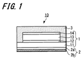
有機EL素子10は、有機EL素子本体部1と、光取り出しシート2と、封止材3とを備える。有機EL素子本体部1は、素子基板11と、陽極12(第1電極)と、有機化合物層13と、陰極14(第2電極)とを備える。そして、本実施形態では、光取り出しシート2は、素子基板11の陽極12側とは反対側の面上に設けられ、封止材3は、有機EL素子本体部1の陽極12、有機化合物層13、及び、陰極14を覆うように設けられる。
The
なお、本実施形態の有機EL素子10では、陽極12側から発光光を取り出す例を説明するが、本発明はこれに限定されず、陰極14側から、又は、陽極12側及び陰極14側の両方から発光光を取り出す構成にしてもよい。この場合、有機EL素子10の陰極14側の光取り出し面にも、光取り出しシート2を設けてもよい。
In addition, although the
また、有機化合物層13は、発光層を含む層であるが、発光層以外にも、例えば、キャリア(正孔及び電子)の注入層、阻止層及び輸送層等の各種有機層を備え、これらの各種有機層を積層して構成される。
The
有機EL素子本体部1を構成する各部及び各層の好ましい積層例は、次の通りである。
(1)素子基板/陽極/発光層/電子輸送層/陰極
(2)素子基板/陽極/正孔輸送層/発光層/電子輸送層/陰極
(3)素子基板/陽極/正孔輸送層/発光層/正孔阻止層/電子輸送層/陰極
(4)素子基板/陽極/正孔輸送層/発光層/正孔阻止層/電子輸送層/電子注入層(陰極バッファー層)/陰極
(5)素子基板/陽極/正孔注入層(陽極バッファー層)/正孔輸送層/発光層/正孔阻止層/電子輸送層/電子注入層/陰極
(6)素子基板/陽極/正孔注入層/正孔輸送層/発光層/電子輸送層/電子注入層/陰極
以下、有機EL素子10の各部及び各層の構成をより具体的に説明する。The preferable lamination example of each part and each layer which comprises the organic EL element main-
(1) Element substrate / anode / light emitting layer / electron transport layer / cathode (2) Element substrate / anode / hole transport layer / light emitting layer / electron transport layer / cathode (3) Element substrate / anode / hole transport layer / Light emitting layer / hole blocking layer / electron transport layer / cathode (4) element substrate / anode / hole transport layer / light emitting layer / hole blocking layer / electron transport layer / electron injection layer (cathode buffer layer) / cathode (5 ) Element substrate / anode / hole injection layer (anode buffer layer) / hole transport layer / light emitting layer / hole blocking layer / electron transport layer / electron injection layer / cathode (6) Element substrate / anode / hole injection layer / Hole transport layer / light emitting layer / electron transport layer / electron injection layer / cathode Hereinafter, each part of the
[素子基板]
素子基板11(基体、基板、基材、支持体)は、例えば、ガラス、プラスチック等の透明性材料で形成することができる。特に、素子基板11を、ガラス基板、薄膜ガラス、石英基板、又は、透明樹脂フィルムで構成することが好ましい。[Element substrate]
The element substrate 11 (base, substrate, base, support) can be formed of a transparent material such as glass or plastic. In particular, the
透明樹脂フィルムの形成材料としては、例えば、ポリエチレンテレフタレート(PET)、ポリエチレンナフタレート(PEN)等のポリエステルを用いることができる。また、透明樹脂フィルムの形成材料としては、例えば、ポリエチレン、ポリプロピレン、セロファン等の材料を用いることができる。さらに、セルロースジアセテート、セルローストリアセテート、セルロースアセテートブチレート、セルロースアセテートプロピオネート(CAP)、セルロースアセテートフタレート(TAC)、セルロースナイトレート等のセルロースエステル類、又は、それらの誘導体を透明樹脂フィルムの形成材料として用いることができる。 As a material for forming the transparent resin film, for example, polyester such as polyethylene terephthalate (PET) or polyethylene naphthalate (PEN) can be used. Moreover, as a formation material of a transparent resin film, materials, such as polyethylene, a polypropylene, a cellophane, can be used, for example. Furthermore, cellulose diacetate, cellulose triacetate, cellulose acetate butyrate, cellulose acetate propionate (CAP), cellulose acetate phthalate (TAC), cellulose esters such as cellulose nitrate, or their derivatives are formed into a transparent resin film. It can be used as a material.
また、透明樹脂フィルムの形成材料としては、例えば、ポリ塩化ビニリデン、ポリビニルアルコール、ポリエチレンビニルアルコール、シンジオタクティックポリスチレン、ポリカーボネート、ノルボルネン樹脂、ポリメチルペンテン、ポリエーテルケトン、ポリイミド、ポリエーテルスルホン(PES)、ポリフェニレンスルフィド、ポリスルホン類、ポリエーテルイミド、ポリエーテルケトンイミド、ポリアミド、フッ素樹脂、ナイロン、ポリメチルメタクリレート、アクリル、ポリアリレート類等の材料を用いることができる。さらに、例えば、アートン(登録商標:JSR社製)、又は、アペル(登録商標:三井化学社製)と呼ばれるシクロオレフィン系樹脂を透明樹脂フィルムの形成材料として用いることもできる。 Examples of the material for forming the transparent resin film include polyvinylidene chloride, polyvinyl alcohol, polyethylene vinyl alcohol, syndiotactic polystyrene, polycarbonate, norbornene resin, polymethylpentene, polyether ketone, polyimide, and polyether sulfone (PES). , Polyphenylene sulfide, polysulfones, polyether imide, polyether ketone imide, polyamide, fluororesin, nylon, polymethyl methacrylate, acrylic, polyarylate, and the like can be used. Furthermore, for example, a cycloolefin resin called Arton (registered trademark: manufactured by JSR) or Apel (registered trademark: manufactured by Mitsui Chemicals) can be used as a material for forming a transparent resin film.
素子基板11としてポリイミドフィルムを用いる場合には、貯蔵弾性率が約2〜10GPaの範囲内の値であり、かつ、熱膨張係数が約0〜6ppmの範囲内の値であるという条件を満たす非熱可塑性ポリイミドフィルムであれば、任意のポリイミドフィルムを素子基板11として用いることができる。それゆえ、素子基板11として、従来公知のポリイミドフィルムを使用することができ、例えば、XENOMAX(登録商標:東洋紡績(株)製)や、ポミラン(登録商標)T(荒川化学工業(株)製)などの市販のポリイミドフィルムを用いることができる。なお、ポリイミドフィルムの作製手法としては、例えば、特開平5−70590号公報、特開2000−119419号公報、同2007−56198号公報、同2005−68408号公報等に記載されている従来公知の手法を用いることができる。
In the case where a polyimide film is used as the
また、素子基板11を上記各種材料からなる透明樹脂フィルムで構成した場合、有機EL素子10内への例えば水蒸気、酸素等の透過を抑制するために、透明樹脂フィルムの表面に、無機材料からなる被膜、有機材料からなる被膜、又は、これらの被膜を積層したハイブリッド被膜を設けてもよい。この場合には、水蒸気透過度(環境条件:25±0.5℃、相対湿度(90±2)%RH)が約0.01g/[m2・day・atm]以下の値となるようなバリア性フィルムで上記被膜を構成することが好ましい。また、上記被膜を、酸素透過度が約10−3cm3/[m2・day・atm]以下の値であり、かつ、水蒸気透過度が約10−3g/[m2・day・atm]以下の値となるようなバリア性フィルムで構成することがより好ましい。さらに、上記被膜を、酸素透過度が約10−3cm3/[m2・day・atm]以下の値であり、かつ、水蒸気透過度が約10−5g/[m2・day・atm]以下の値となるようなバリア性フィルムで構成することが特に好ましい。なお、本明細書でいう「水蒸気透過度」は、JIS(日本工業規格)−K7129(1992年)に準拠した赤外センサー法により測定された値であり、「酸素透過度」は、JIS−K7126(1987年)に準拠したクーロメトリック法により測定された値である。Further, when the
上述したバリア性フィルム(上記被膜)の形成材料としては、有機EL素子10の劣化を招く、例えば水分、酸素等の因子の有機EL素子10への浸入を抑制できる材料であれば、任意の材料を用いることができる。例えば、バリア性フィルムを、酸化ケイ素、二酸化ケイ素、窒化ケイ素等の無機材料からなる被膜で構成することができる。なお、バリア性フィルムの脆弱性を改良するためには、上記無機材料からなる被膜と有機材料からなる被膜とを積層したハイブリッド被膜でバリア性フィルムを構成することが好ましい。この場合、無機材料からなる被膜及び有機材料からなる被膜の積層順序は任意であるが、両者を交互に複数回積層することが好ましい。
As a material for forming the above-described barrier film (the coating film), any material can be used as long as it can suppress deterioration of the
また、上述のようなバリア性フィルムの形成手法としては、バリア性フィルムを素子基板11(透明樹脂フィルム)上に形成できる手法であれば任意の手法を用いることができる。例えば、真空蒸着法、スパッタリング法、反応性スパッタリング法、分子線エピタキシー法、クラスタ−イオンビーム法、イオンプレーティング法、プラズマ重合法、大気圧プラズマ重合法(特開2004−68143号公報参照)、プラズマCVD(Chemical Vapor Deposition)法、レーザーCVD法、熱CVD法、コーティング法等の手法を用いることができる。なお、本実施形態では、特に、大気圧プラズマ重合法を用いることが好ましい。 In addition, as a method for forming the barrier film as described above, any method can be used as long as the barrier film can be formed on the element substrate 11 (transparent resin film). For example, vacuum deposition method, sputtering method, reactive sputtering method, molecular beam epitaxy method, cluster ion beam method, ion plating method, plasma polymerization method, atmospheric pressure plasma polymerization method (see JP 2004-68143 A), Techniques such as plasma CVD (Chemical Vapor Deposition), laser CVD, thermal CVD, and coating can be used. In the present embodiment, it is particularly preferable to use an atmospheric pressure plasma polymerization method.
さらに、本実施形態では、素子基板11を、メタルフォイルで構成してもよい。メタルフォイルとしては、例えば、アルミニウム箔、銅箔、ステンレス箔、金箔、銀箔等の金属箔を用いることができる。なお、金属箔の厚さは、約10〜100μmの範囲内の値で設定することが好ましい。
Furthermore, in the present embodiment, the
また、素子基板11としてメタルフォイルを用いる場合、メタルフォイルの片面又は両面に絶縁層を設けることが好ましい。絶縁層は、例えば、無機酸化物や無機窒化物などの無機物、ポリエチレンテレフタレート、ポリブチレンフタレート、ポリエチレンナフタレート等のポリエステル、ポリスチレン、ポリカーボネート、ポリエーテルスルホン、ポリアリレート、アリルジグリコールカーボネート、ポリイミド、ポリシクロオレフィン、ノルボルネン樹脂、ポリ(クロロトリフルオロエチレン)、ポリイミド等で形成することができる。
Further, when a metal foil is used as the
絶縁層として無機絶縁層を用いる場合には、無機絶縁層を、例えば、酸化珪素、酸化ゲルマニウム、酸化亜鉛、酸化アルミニウム、酸化チタン、酸化銅等からなる金属酸化物膜や、窒化珪素、窒化ゲルマニウム、窒化アルミニウム等からなる金属窒化物膜で構成することが好ましい。また、これらの各種無機膜から一種又は二種以上の膜を組合せて絶縁層を構成してもよい。なお、無機絶縁層の膜厚は、約10〜100nmの範囲内の値で設定することが好ましい。また、金属酸化物及び/又は金属窒化物からなる絶縁層を成膜する手法としては、任意の手法を用いることができ、例えば、蒸着法、スパッタリング法、CVD(Chemical Vapor Deposition)法等の乾式法、ゾル−ゲル法等の湿式法、金属酸化物及び/又は金属窒化物の粒子を溶剤に分散させた溶液を塗布する手法等を利用することができる。 In the case where an inorganic insulating layer is used as the insulating layer, the inorganic insulating layer is made of, for example, a metal oxide film made of silicon oxide, germanium oxide, zinc oxide, aluminum oxide, titanium oxide, copper oxide, silicon nitride, germanium nitride, or the like. It is preferable to use a metal nitride film made of aluminum nitride or the like. Moreover, you may comprise an insulating layer combining 1 type, or 2 or more types of films from these various inorganic films. In addition, it is preferable to set the film thickness of an inorganic insulating layer by the value within the range of about 10-100 nm. In addition, as a method for forming an insulating layer made of a metal oxide and / or a metal nitride, any method can be used. For example, a dry method such as a vapor deposition method, a sputtering method, a CVD (Chemical Vapor Deposition) method, or the like. Methods, wet methods such as a sol-gel method, a method of applying a solution in which metal oxide and / or metal nitride particles are dispersed in a solvent can be used.
なお、絶縁層をメタルフォイルの両面に設ける場合には、金属酸化物及び/又は金属窒化物からなる絶縁層を、メタルフォイルの両面に設けてもよいし、ポリイミドシートのようなプラスチック絶縁層を、メタルフォイルの両面に設けてもよい。また、メタルフォイルの一方の面に、金属酸化物及び/又は金属窒化物からなる絶縁層を設け、他方の面にポリイミドシートのようなプラスチック絶縁層を設けてもよい。 In addition, when providing an insulating layer on both surfaces of a metal foil, you may provide the insulating layer which consists of a metal oxide and / or a metal nitride on both surfaces of a metal foil, or a plastic insulating layer like a polyimide sheet is provided. The metal foil may be provided on both sides. Further, an insulating layer made of a metal oxide and / or a metal nitride may be provided on one surface of the metal foil, and a plastic insulating layer such as a polyimide sheet may be provided on the other surface.
[陽極]
陽極12は、発光層に正孔を供給(注入)する電極膜であり、仕事関数の大きい(4eV以上)、例えば、金属、合金、電気伝導性化合物、及び、これらの混合物等の電極材料で形成される。[anode]
The
なお、陽極12の屈折率は任意であるが、約1.5〜2.0の範囲内の値であることが好ましく、約1.55〜1.85の範囲内の値であることが特に好ましい。また、陽極12のシート抵抗(表面抵抗)は数百Ω/sq.以下の値であることが好ましい。さらに、陽極12の膜厚は、形成材料に依存して変化するが、通常、約10〜1000nm、好ましくは約10〜200nmの範囲内の値に設定される。
The refractive index of the
このような特性を有する電極材料としては、例えば、Au等の金属や、CuI、ITO(Indium Tin Oxide)、SnO2、ZnO等の金属化合物などの光透過性を有する電極材料を用いることができる。また、陽極12は、例えばIDIXO(登録商標:In2O3−ZnO)等の非晶質の透明電極材料で形成することもできる。As an electrode material having such characteristics, for example, a light transmissive electrode material such as a metal such as Au or a metal compound such as CuI, ITO (Indium Tin Oxide), SnO 2 , or ZnO can be used. . The
陽極12は、上述した電極材料を蒸着やスパッタすることにより形成される。この際、フォトリソグラフィー技術を用いて、陽極12を所望の形状パターンで形成してもよい。なお、陽極12において、その形状パターンの精度を必要としない場合(精度が100μm以上程度の場合)には、陽極12を例えば蒸着やスパッタリングなどの手法により形成する際に、所望の形状パターンが形成されたマスクを用いて、所望パターンの陽極12を形成してもよい。
The
また、陽極12は、有機導電性化合物で形成することもできる。この場合、有機導電性化合物は塗布可能な物質であるので、例えば、印刷方式、コーティング方式等の湿式成膜手法を用いて、陽極12を形成することができる。
The
[有機化合物層]
有機化合物層13は、上述のように、発光層だけでなく、キャリア(正孔及び電子)の注入層、阻止層及び輸送層等の各種有機層を備える。ここで、各有機層の構成をより具体的に説明する。[Organic compound layer]
As described above, the
(1)発光層
発光層は、陽極12から直接、又は、陽極12から正孔輸送層等を介して注入される正孔と、陰極14から直接、又は、陰極14から電子輸送層等を介して注入される電子とが再結合して発光する層である。なお、発光する部分は、発光層の内部であってもよいし、発光層と、それに隣接する層との間の界面であってもよい。(1) Light-Emitting Layer The light-emitting layer is directly injected from the
また、発光層は、一層で構成してもよいし、複数の層を積層して構成してもよい。発光層を複数の層で構成する場合には、同一の発光スペクトルや発光極大波長を有する層を複数積層してもよいし、互いに異なる発光スペクトルや発光極大波長を有する層を複数積層してもよい(例えば、青、緑、赤等の各色発光層で発光層を構成する)。なお、後者の場合には、隣り合う発光層間に、非発光性の中間層を設けることが好ましい。 In addition, the light emitting layer may be composed of a single layer or a plurality of layers stacked. When the light emitting layer is composed of a plurality of layers, a plurality of layers having the same emission spectrum or maximum emission wavelength may be laminated, or a plurality of layers having different emission spectra or emission maximum wavelengths may be laminated. Good (for example, the light emitting layer is composed of light emitting layers of blue, green, red, etc.). In the latter case, it is preferable to provide a non-light emitting intermediate layer between adjacent light emitting layers.
本実施形態では、発光層を、ホスト化合物(ホスト材料)と、発光材料(発光ドーパント化合物)とを含む有機発光性材料で形成する。このような構成の発光層では、発光材料の発光波長や含有させる発光材料の種類等を適宜調整することにより任意の発光色を得ることができる。また、本実施形態では、発光材料で発光させることが好ましい。 In the present embodiment, the light emitting layer is formed of an organic light emitting material including a host compound (host material) and a light emitting material (light emitting dopant compound). In the light emitting layer having such a configuration, an arbitrary emission color can be obtained by appropriately adjusting the emission wavelength of the light emitting material, the type of the light emitting material to be contained, and the like. Moreover, in this embodiment, it is preferable to make it light-emit with a luminescent material.
発光層の膜厚の総和は、例えば必要とする発光特性等に応じて適宜設定することができる。例えば、構成膜の均質性、発光時における不必要な高電圧の印加の防止、及び、駆動電流に対する発光色の安定性向上等の観点では、発光層の膜厚の総和を、例えば、約1〜200nmの範囲内の値に設定することが好ましい。特に、低駆動電圧の観点では、発光層の膜厚の総和を約30nm以下の値に設定することが好ましい。 The total thickness of the light emitting layers can be set as appropriate according to, for example, required light emission characteristics. For example, in terms of uniformity of constituent films, prevention of unnecessary application of high voltage during light emission, and improvement in stability of light emission color with respect to drive current, the total thickness of the light emitting layers is, for example, about 1 It is preferable to set the value within a range of ˜200 nm. In particular, from the viewpoint of a low driving voltage, it is preferable to set the total thickness of the light emitting layers to a value of about 30 nm or less.
なお、発光層を複数の層で構成し、かつ、隣り合う該層間に中間層を設けた場合には、中間層を含む発光層全体の厚さを上記数値範囲内の値に設定することが好ましい。また、発光層を複数の層で構成する場合、各層の膜厚を、約1〜50nmの範囲内の値に設定することが好ましく、約1〜20nmの範囲内の値に設定することがさらに好ましい。なお、発光層を複数の層で構成する場合には、各層間の膜厚関係は、任意に設定することができる。 When the light emitting layer is composed of a plurality of layers and an intermediate layer is provided between the adjacent layers, the thickness of the entire light emitting layer including the intermediate layer may be set to a value within the above numerical range. preferable. When the light emitting layer is composed of a plurality of layers, the thickness of each layer is preferably set to a value in the range of about 1 to 50 nm, and more preferably set to a value in the range of about 1 to 20 nm. preferable. When the light emitting layer is composed of a plurality of layers, the film thickness relationship between the layers can be arbitrarily set.
上述のような構成の発光層は、例えば、真空蒸着法、スピンコート法、キャスト法、LB(Langmuir-Blodgett)法、インクジェット法等の公知の薄膜形成手法を用いて形成することができる。以下、発光層に含まれるホスト化合物及び発光材料の構成について具体例に説明する。 The light emitting layer having the above-described configuration can be formed using a known thin film forming method such as a vacuum deposition method, a spin coating method, a casting method, an LB (Langmuir-Blodgett) method, an ink jet method, or the like. Hereinafter, the configuration of the host compound and the light emitting material contained in the light emitting layer will be described with specific examples.
(a)ホスト化合物
発光層に含まれるホスト化合物としては、室温(25℃)における燐光発光の燐光量子収率が約0.1未満の値である化合物を用いることが好ましい。特に、燐光量子収率が約0.01未満の値である化合物をホスト化合物として用いることが好ましい。また、発光層中のホスト化合物の体積比は、発光層に含まれる各種化合物の中で約50%以上の値とすることが好ましい。(A) Host compound As the host compound contained in the light emitting layer, a compound having a phosphorescence quantum yield of phosphorescence emission at room temperature (25 ° C.) of less than about 0.1 is preferably used. In particular, a compound having a phosphorescence quantum yield of less than about 0.01 is preferably used as the host compound. The volume ratio of the host compound in the light emitting layer is preferably about 50% or more among various compounds contained in the light emitting layer.
また、ホスト化合物としては、公知のホスト化合物を用いることができる。その際、一種類のホスト化合物を用いてもよいし、複数種のホスト化合物を併用してもよい。複数種のホスト化合物を用いることにより、電荷(正孔及び/又は電子)の移動度(移動量)を調整することができ、有機EL素子10の発光効率を向上させることができる。
A known host compound can be used as the host compound. At that time, one type of host compound may be used, or a plurality of types of host compounds may be used in combination. By using a plurality of types of host compounds, the mobility (movement amount) of electric charges (holes and / or electrons) can be adjusted, and the light emission efficiency of the
上述のような特性を有するホスト化合物としては、例えば、公知の低分子化合物、繰り返し単位をもつ高分子化合物、ビニル基やエポキシ基のような重合性基を有する低分子化合物(蒸着重合性発光ホスト)等の化合物を用いることができる。なお、ホスト化合物としては、正孔輸送機能、電子輸送機能、発光の長波長化を防止する機能、及び、高Tg(ガラス転移温度)を有する化合物を用いることが好ましい。なお、ここでいう、「ガラス転移温度(Tg)」とは、DSC(Differential Scanning Calorimetry:示差走査熱量)法を用いて、JIS−K7121に準拠した手法により求められる値である。 Examples of the host compound having the above-described characteristics include known low-molecular compounds, high-molecular compounds having repeating units, and low-molecular compounds having a polymerizable group such as a vinyl group or an epoxy group (evaporation polymerizable light-emitting host). ) And the like can be used. As the host compound, it is preferable to use a compound having a hole transporting function, an electron transporting function, a function of preventing emission of longer wavelengths, and a high Tg (glass transition temperature). The “glass transition temperature (Tg)” here is a value obtained by a method based on JIS-K7121 using a DSC (Differential Scanning Calorimetry) method.
具体的には、ホスト化合物として、例えば、特開2001−257076号公報、同2002−308855号公報、同2001−313179号公報、同2002−319491号公報、同2001−357977号公報、同2002−334786号公報、同2002−8860号公報、同2002−334787号公報、同2002−15871号公報、同2002−334788号公報、同2002−43056号公報、同2002−334789号公報、同2002−75645号公報、同2002−338579号公報、同2002−105445号公報、同2002−343568号公報、同2002−141173号公報、同2002−352957号公報、同2002−203683号公報、同2002−363227号公報、同2002−231453号公報、同2003−3165号公報、同2002−234888号公報、同2003−27048号公報、同2002−255934号公報、同2002−260861号公報、同2002−280183号公報、同2002−299060号公報、同2002−302516号公報、同2002−305083号公報、同2002−305084号公報、同2002−308837号公報等の文献に記載されている化合物を用いることができる。 Specifically, as host compounds, for example, Japanese Patent Application Laid-Open Nos. 2001-257076, 2002-308855, 2001-313179, 2002-319491, 2001-357777, 2002 No. 334786, No. 2002-8860, No. 2002-334787, No. 2002-15871, No. 2002-334788, No. 2002-43056, No. 2002-334789, No. 2002-75645. Gazette, 2002-338579 gazette, 2002-105445 gazette, 2002-343568 gazette, 2002-141173 gazette, 2002-352957 gazette, 2002-203683 gazette, 2002-363227 gazette. No. 2002-231453, No. 2003-3165, No. 2002-234888, No. 2003-27048, No. 2002-255934, No. 2002-260861, No. 2002-280183. , 2002-299060, 2002-302516, 2002-305083, 2002-305084, 2002-308837, and the like can be used.
なお、本実施形態では、ホスト化合物は、カルバゾール誘導体であることが好ましく、特に、カルバゾール誘導体であって、かつ、ジベンゾフラン化合物であることが好ましい(例えば、後述の各種実施例で用いる構造式(1)H−Aを有するホスト化合物)。 In this embodiment, the host compound is preferably a carbazole derivative, and particularly preferably a carbazole derivative and a dibenzofuran compound (for example, structural formulas (1) used in various examples described later. ) Host compound with H-A).
(b)発光材料
発光材料としては、例えば、燐光発光材料(燐光性化合物、燐光発光性化合物)、蛍光発光材料等を用いることができる。なお、一つの発光層には、一種類の発光材料を含有させてもよいし、発光極大波長が互いに異なる複数種の発光材料を含有させてもよい。複数種の発光材料を用いることにより、上述のように、発光波長の異なる複数の光を混ぜることができ、これにより、任意の発光色の光を得ることができる。例えば、青色発光材料、緑色発光材料及び赤色発光材料(3種類の発光発光材料)を発光層に含有させることにより白色光を得ることができる。(B) Light emitting material As the light emitting material, for example, a phosphorescent light emitting material (phosphorescent compound, phosphorescent light emitting compound), a fluorescent light emitting material, or the like can be used. Note that one light emitting layer may contain one kind of light emitting material, or may contain a plurality of kinds of light emitting materials having different light emission maximum wavelengths. By using a plurality of types of light emitting materials, it is possible to mix a plurality of lights having different emission wavelengths as described above, thereby obtaining light of an arbitrary emission color. For example, white light can be obtained by including a blue light emitting material, a green light emitting material, and a red light emitting material (three kinds of light emitting light emitting materials) in the light emitting layer.
また、一つの発光層に、燐光発光材料及び蛍光発光材料を混合してもよい。さらに、本実施形態では、一つの発光層に2種以上の発光材料を含有させる場合には、発光層における発光材料の濃度比を発光層の厚さ方向において変化させてもよい。 Further, a phosphorescent material and a fluorescent material may be mixed in one light emitting layer. Furthermore, in this embodiment, when two or more light emitting materials are contained in one light emitting layer, the concentration ratio of the light emitting materials in the light emitting layer may be changed in the thickness direction of the light emitting layer.
燐光発光材料は、励起三重項からの発光が得られる化合物である。具体的には、燐光発光材料は、室温(25℃)において燐光発光する化合物であり、燐光量子収率が、25℃において約0.01以上の値の化合物である。なお、本実施形態では、燐光量子収率が約0.1以上の値である燐光発光材料を用いることが好ましい。燐光量子収率は、例えば、「第4版実験化学講座7・分光II」(1992年版、丸善)の398頁に記載されている手法により測定することができる。また、溶液中での燐光量子収率は種々の溶媒を用いて測定できるが、本実施形態では、燐光発光材料が、任意の溶媒において、約0.01以上の燐光量子収率が得られる燐光発光材料であればよい。
A phosphorescent material is a compound that can emit light from an excited triplet. Specifically, the phosphorescent material is a compound that emits phosphorescence at room temperature (25 ° C.), and is a compound having a phosphorescence quantum yield of about 0.01 or more at 25 ° C. In the present embodiment, it is preferable to use a phosphorescent material having a phosphorescence quantum yield of about 0.1 or more. The phosphorescence quantum yield can be measured, for example, by the method described on page 398 of "4th edition
上述したホスト化合物及び燐光発光材料を含む発光層における発光(燐光発光)の過程(原理)としては、次の2種類の過程が挙げられる。 As the process (principle) of light emission (phosphorescence emission) in the light emitting layer containing the host compound and the phosphorescent light emitting material, the following two kinds of processes can be mentioned.
第1の発光過程は、エネルギー移動型の発光過程である。このタイプの発光過程では、まず、キャリア(正孔及び電子)が輸送される発光層内のホスト化合物上において、キャリアが再結合し、これにより、燐光発光材料の励起状態が生成される。そして、この際に発生するエネルギーがホスト化合物から燐光発光材料に移動し(励起状態のエネルギー準位がホスト化合物の励起準位から燐光発光材料の励起準位(励起三重項)に移動し)、この結果、燐光発光材料から発光が生じる。 The first light emission process is an energy transfer type light emission process. In this type of light emission process, first, carriers recombine on the host compound in the light emitting layer to which carriers (holes and electrons) are transported, thereby generating an excited state of the phosphorescent material. And the energy generated at this time moves from the host compound to the phosphorescent material (the energy level in the excited state moves from the excited level of the host compound to the excited level (excited triplet) of the phosphorescent material), As a result, light emission occurs from the phosphorescent material.
第2の発光過程は、キャリアトラップ型の発光過程である。このタイプの発光過程では、発光層において、燐光発光材料がキャリア(正孔及び電子)をトラップする。その結果、燐光発光材料上でキャリアの再結合が起こり、燐光発光材料から発光が生じる。上述したいずれの発光過程においても、燐光発光材料の励起状態のエネルギー準位はホスト化合物の励起状態のエネルギー準位より低くする必要がある。 The second light emission process is a carrier trap type light emission process. In this type of light emission process, the phosphorescent material traps carriers (holes and electrons) in the light emitting layer. As a result, carrier recombination occurs on the phosphorescent material, and light is emitted from the phosphorescent material. In any of the light emission processes described above, the energy level in the excited state of the phosphorescent material needs to be lower than the energy level in the excited state of the host compound.
上述のような発光過程を生じさせる燐光発光材料としては、従来の有機EL素子で用いられる公知の各種燐光発光材料の中から所望の燐光発光材料を適宜選択して用いることができる。例えば、燐光発光材料としては、元素の周期表で8族〜10族の金属元素を含有する錯体系化合物を用いることができる。そのような錯体系化合物の中でも、イリジウム化合物、オスミウム化合物、白金化合物(白金錯体系化合物)、及び、希土類錯体のいずれかを燐光発光材料として用いることが好ましい。本実施形態では、特に、燐光発光材料として、イリジウム化合物(例えば、後述の各種実施例で用いる構造式(2)〜(4)を有する燐光発光材料)を用いることが好ましい。
As the phosphorescent material that causes the above-described light emission process, a desired phosphorescent material can be appropriately selected from various known phosphorescent materials used in conventional organic EL elements. For example, as the phosphorescent material, a complex compound containing a metal element of
また、蛍光発光材料(蛍光発光体、蛍光性ドーパント)としては、例えば、クマリン系色素、ピラン系色素、シアニン系色素、クロコニウム系色素、スクアリウム系色素、オキソベンツアントラセン系色素、フルオレセイン系色素、ローダミン系色素、ピリリウム系色素、ペリレン系色素、スチルベン系色素、ポリチオフェン系色素、又は希土類錯体系蛍光体等を用いることができる。 Examples of fluorescent light-emitting materials (fluorescent light emitters and fluorescent dopants) include, for example, coumarin dyes, pyran dyes, cyanine dyes, croconium dyes, squalium dyes, oxobenzanthracene dyes, fluorescein dyes, rhodamines. A dye, a pyrylium dye, a perylene dye, a stilbene dye, a polythiophene dye, a rare earth complex phosphor, or the like can be used.
さらに、蛍光発光材料としては、例えば、国際公開第00/70655号パンフレット、特開2002−280178号公報、同2001−181616号公報、同2002−280179号公報、同2001−181617号公報、同2002−280180号公報、同2001−247859号公報、同2002−299060号公報、同2001−313178号公報、同2002−302671号公報、同2001−345183号公報、同2002−324679号公報、国際公開第02/15645号パンフレット、特開2002−332291号公報、同2002−50484号公報、同2002−332292号公報、同2002−83684号公報、特表2002−540572号公報、特開2002−117978号公報、同2002−338588号公報、同2002−170684号公報、同2002−352960号公報、国際公開第01/93642号パンフレット、特開2002−50483号公報、同2002−100476号公報、同2002−173674号公報、同2002−359082号公報、同2002−175884号公報、同2002−363552号公報、同2002−184582号公報、同2003−7469号公報、特表2002−525808号公報、特開2003−7471号公報、特表2002−525833号公報、特開2003−31366号公報、同2002−226495号公報、同2002−234894号公報、同2002−235076号公報、同2002−241751号公報、同2001−319779号公報、同2001−319780号公報、同2002−62824号公報、同2002−100474号公報、同2002−203679号公報、同2002−343572号公報、同2002−203678号公報等に記載の従来公知の蛍光発光材料も用いることができる。 Furthermore, examples of the fluorescent light-emitting material include, for example, International Publication No. 00/70655 pamphlet, Japanese Patent Application Laid-Open Nos. 2002-280178, 2001-181616, 2002-280179, 2001-181617, 2002. No. -280180, No. 2001-247859, No. 2002-299060, No. 2001-313178, No. 2002-302671, No. 2001-345183, No. 2002-324679, International Publication No. No. 02/15645, JP 2002-332291, 2002-50484, 2002-332292, 2002-83684, JP 2002-540572, JP 2002-117978 2002-338588, 2002-170684, 2002-352960, WO 01/93642, JP-A 2002-50483, 2002-100476, 2002-173684. Publication No. 2002-359082 Publication No. 2002-175484 Publication No. 2002-363552 Publication No. 2002-184582 Publication No. 2003-7469 Publication No. 2002-525808 Publication No. 7471, JP 2002-525833, JP 2003-31366, 2002-226495, 2002-234894, 2002-233506, 2002-241751, 2001. -3 No. 9779, No. 2001-319780, No. 2002-62824, No. 2002-1000047, No. 2002-203679, No. 2002-343572, No. 2002-203678, etc. Known fluorescent materials can also be used.
(c)中間層
上述のように、発光層を複数の層で構成した場合、隣り合う層間に、非発光性の中間層(非ドープ領域)を設けることが好ましい。この場合、中間層の膜厚を、約1〜20nmの範囲内の値に設定することが好ましい。特に、中間層と隣接する発光層との間におけるエネルギー移動等の相互作用の抑制、及び、有機EL素子10の電流電圧特性への影響の低減という観点では、中間層の膜厚は、約3〜10nmの範囲内の値で設定することが好ましい。(C) Intermediate layer As described above, when the light emitting layer is composed of a plurality of layers, it is preferable to provide a non-light emitting intermediate layer (undoped region) between adjacent layers. In this case, it is preferable to set the film thickness of the intermediate layer to a value within the range of about 1 to 20 nm. In particular, from the viewpoint of suppressing the interaction such as energy transfer between the intermediate layer and the adjacent light emitting layer and reducing the influence on the current-voltage characteristics of the
中間層の形成材料としては、発光層内のホスト化合物と同様の材料で形成することができる。なお、中間層を設ける場合、中間層の形成材料は、隣接する発光層のホスト化合物の形成材料と同一であってもよいし、異なっていてもよいが、隣接する2つの発光層のうち、少なくとも一方の発光層のホスト化合物の形成材料と同一であることが好ましい。 The intermediate layer can be formed of the same material as the host compound in the light emitting layer. In the case of providing the intermediate layer, the formation material of the intermediate layer may be the same as or different from the formation material of the host compound of the adjacent light emitting layer, but of the two adjacent light emitting layers, It is preferably the same as the host compound forming material of at least one light emitting layer.
このように、中間層(非ドープ発光層)と各発光層との間に共通の化合物を含有させた場合、次のような利点が得られる。例えば両者間において、共通のホスト材料を用いた場合(ここでいう、ホスト材料が共通であるとは、ホスト材料の分子構造が同一である場合だけでなく、ホスト材料の燐光発光エネルギー、ガラス転移点等の物理化学的特性が同一である場合等も含む意味である)には、発光層及び中間層間の界面におけるキャリアの注入障壁が低減され、電圧(電流)を変化させても正孔及び電子間の注入バランスが保たれ易いという効果が得られる。さらに、中間層と発光層との間で共通のホスト材料を用いた場合には、従来の有機EL素子の作製において大きな問題点となっていた素子作製の煩雑さも併せて解消することができる。 Thus, when a common compound is contained between the intermediate layer (undoped light emitting layer) and each light emitting layer, the following advantages are obtained. For example, when a common host material is used between the two (here, the common host material means not only the case where the molecular structure of the host material is the same, but also the phosphorescence energy of the host material, the glass transition In other words, the barrier for injecting carriers at the interface between the light emitting layer and the intermediate layer is reduced, and even if the voltage (current) is changed, holes and The effect that the injection balance between electrons is easily maintained is obtained. Furthermore, when a common host material is used between the intermediate layer and the light emitting layer, the complexity of device fabrication, which has been a major problem in the fabrication of conventional organic EL devices, can also be eliminated.
なお、本実施形態では、ホスト材料はキャリアの輸送を担うため、キャリア輸送能を有する材料が好ましい。このキャリア輸送能を表す物性としてはキャリア移動度が用いられ、有機材料のキャリア移動度は、一般に、電界強度に依存する。それゆえ、電界強度依存性の高い材料をホスト材料を用いた場合には、正孔及び電子間の注入バランスが崩れやすいので、発光層のホスト化合物及び中間層の形成材料としては、キャリア移動度の電界強度依存性の小さいホスト材料を用いることが好ましい。また、正孔及び電子間の注入バランスを最適に調整するために、非発光性の中間層を、後述するキャリアの阻止層(正孔阻止層、電子阻止層)として機能させてもよい。 In this embodiment, since the host material is responsible for carrier transportation, a material having carrier transportation ability is preferable. Carrier mobility is used as a physical property representing this carrier transport ability, and the carrier mobility of an organic material generally depends on the electric field strength. Therefore, when a host material is used as a material having a high electric field strength dependency, the injection balance between holes and electrons is easily lost. It is preferable to use a host material having a small dependence on the electric field strength. In order to optimally adjust the injection balance between holes and electrons, the non-light emitting intermediate layer may function as a carrier blocking layer (hole blocking layer, electron blocking layer) described later.
(2)注入層(正孔注入層、電子注入層)
有機化合物層13内には、必要に応じて、キャリアの注入層(正孔注入層及び/電子輸送層)が設けられる。注入層は、駆動電圧の低下や発光輝度の向上を図るための層であり、電極及び有機層(発光層)間に設けられる。(2) Injection layer (hole injection layer, electron injection layer)
A carrier injection layer (a hole injection layer and / or an electron transport layer) is provided in the
正孔注入層(陽極バッファー層)は、陽極と、発光層又は正孔輸送層との間に設けられ、電子注入層(陰極バッファー層)は、陰極と、発光層又は電子輸送層との間に設けられる。また、各注入層(バッファー層)は、非常に薄い膜で構成することが望ましく、本実施形態では、形成材料にも依存するが、その膜厚を約0.1nm〜5μmの範囲内の値に設定することが好ましい。 The hole injection layer (anode buffer layer) is provided between the anode and the light emitting layer or the hole transport layer, and the electron injection layer (cathode buffer layer) is provided between the cathode and the light emitting layer or the electron transport layer. Provided. In addition, each injection layer (buffer layer) is preferably composed of a very thin film, and in this embodiment, although depending on the forming material, the film thickness is a value within a range of about 0.1 nm to 5 μm. It is preferable to set to.
なお、各注入層の構成は、例えば、「有機EL素子とその工業化最前線(1998年11月30日エヌ・ティー・エス社発行)」の第2編第2章「電極材料」(123〜166頁)に詳細に記載されている。
The structure of each injection layer is, for example, “Organic EL element and its forefront of industrialization” (issued on November 30, 1998 by NTS Corporation),
また、正孔注入層(陽極バッファー層)の構成は、特開平9−45479号公報、同9−260062号公報、同8−288069号公報等にも詳細に記載されている。具体的には、銅フタロシアニン等を用いて形成されたフタロシアニンバッファー層、酸化バナジウム等を用いて形成された酸化物バッファー層、アモルファスカーボンバッファー層、ポリアニリン(エメラルディン)やポリチオフェン等の導電性高分子を用いて形成された高分子バッファー層などが、正孔注入層として例示されている。なお、後述の各種実施例で説明するように、例えば、PEDOT(ポリ(3,4−エチレンジオキシチオフェン))等を含む化合物を、正孔注入層の形成材料として用いてもよい。 The structure of the hole injection layer (anode buffer layer) is also described in detail in JP-A-9-45479, JP-A-9-260062, JP-A-8-288069 and the like. Specifically, a phthalocyanine buffer layer formed using copper phthalocyanine or the like, an oxide buffer layer formed using vanadium oxide or the like, an amorphous carbon buffer layer, a conductive polymer such as polyaniline (emeraldine) or polythiophene A polymer buffer layer or the like formed using is exemplified as the hole injection layer. In addition, as will be described in various examples described later, for example, a compound containing PEDOT (poly (3,4-ethylenedioxythiophene)) or the like may be used as a material for forming the hole injection layer.
さらに、電子注入層(陰極バッファー層)の構成は、特開平6−325871号公報、同9−17574号公報、同10−74586号公報等にも詳細に記載されている。具体的には、ストロンチウムやアルミニウム等を用いて形成された金属バッファー層、フッ化リチウム、フッ化カリウム等を用いて形成されたアルカリ金属化合物バッファー層、フッ化マグネシウム等を用いて形成されてアルカリ土類金属化合物バッファー層、酸化アルミニウム等を用いて形成された酸化物バッファー層等が電子注入層として例示されている。 Furthermore, the structure of the electron injection layer (cathode buffer layer) is also described in detail in JP-A-6-325871, JP-A-9-17574, JP-A-10-74586, and the like. Specifically, a metal buffer layer formed using strontium, aluminum, etc., an alkali metal compound buffer layer formed using lithium fluoride, potassium fluoride, etc., an alkali formed using magnesium fluoride, etc. Examples of the electron injection layer include an earth metal compound buffer layer, an oxide buffer layer formed using aluminum oxide, and the like.
(3)阻止層(正孔阻止層、電子阻止層)
有機化合物層13内には、必要に応じて、キャリアの阻止層(正孔阻止層及び/又は電子阻止層)が設けられる。なお、阻止層の構成は、例えば、特開平11−204258号公報、同11−204359号公報、及び「有機EL素子とその工業化最前線(1998年11月30日エヌ・ティー・エス社発行)」の237頁等に詳細に記載されている。(3) Blocking layer (hole blocking layer, electron blocking layer)
In the
正孔阻止層(ホールブロック層)は、広い意味で、電子輸送層の機能を有する層であり、電子輸送機能を有しつつ正孔の輸送能力が著しく小さい材料で形成される。このような正孔阻止層を設けることにより、発光層に対する正孔及び電子間の注入バランスを最適な注入バランスに調整することができ、その結果、電子と正孔との再結合確率を向上させることができる。また、正孔阻止層の構成として、必要に応じて、後述する電子輸送層の構成を用いることができる。さらに、正孔阻止層は、発光層に隣接して設けられることが好ましい。 In a broad sense, the hole blocking layer (hole blocking layer) is a layer having a function of an electron transport layer, and is formed of a material having an electron transport function and a remarkably small hole transport capability. By providing such a hole blocking layer, the injection balance between holes and electrons in the light emitting layer can be adjusted to an optimal injection balance, and as a result, the recombination probability between electrons and holes is improved. be able to. Moreover, as a structure of a hole-blocking layer, the structure of the electron carrying layer mentioned later can be used as needed. Furthermore, the hole blocking layer is preferably provided adjacent to the light emitting layer.
一方、電子阻止層は、広い意味で、正孔輸送層の機能を有する層であり、正孔輸送機能を有しつつ電子の輸送能力が著しく小さい材料で形成される。このような電子阻止層を設けることにより、発光層に対する正孔及び電子間の注入バランスを最適な注入バランスに調整することができ、その結果、電子と正孔との再結合確率を向上させることができる。また、電子阻止層の構成として、必要に応じて、後述する正孔輸送層の構成を用いることができる。 On the other hand, the electron blocking layer is a layer having the function of a hole transport layer in a broad sense, and is formed of a material having a hole transport function and a remarkably small electron transport capability. By providing such an electron blocking layer, the injection balance between holes and electrons in the light-emitting layer can be adjusted to an optimal injection balance, and as a result, the recombination probability between electrons and holes can be improved. Can do. Moreover, as a structure of an electron blocking layer, the structure of the positive hole transport layer mentioned later can be used as needed.
なお、各阻止層の膜厚は、約3〜100nmの範囲内の値で設定することが好ましく、約5〜30nmの範囲内の値で設定することがさらに好ましい。 The thickness of each blocking layer is preferably set to a value within the range of about 3 to 100 nm, and more preferably set to a value within the range of about 5 to 30 nm.
(4)輸送層(正孔輸送層、電子輸送層)
有機化合物層13内には、必要に応じて、キャリアの輸送層(正孔輸送層及び/又は電子輸送層)が設けられる。(4) Transport layer (hole transport layer, electron transport layer)
In the
(a)正孔輸送層
正孔輸送層は、陽極12から供給された正孔を発光層に輸送(注入)する層である。また、正孔輸送層は、陰極14側からの電子の流入を阻止する障壁としても作用する。それゆえ、正孔輸送層という用語は、広い意味で、正孔注入層及び/又は電子阻止層を含む意味で用いられることもある。なお、正孔輸送層は、一層だけ設けてもよいし、複数層設けてもよい。(A) Hole Transport Layer The hole transport layer is a layer that transports (injects) holes supplied from the
正孔輸送材料としては、上述した正孔を輸送(注入)する作用、及び、電子の流入を阻止する作用を発現可能な材料であれば、有機材料及び無機材料のいずれの材料も用いることができる。具体的には、正孔輸送材料として、例えば、トリアゾール誘導体、オキサジアゾール誘導体、イミダゾール誘導体、ポリアリールアルカン誘導体、ピラゾリン誘導体、ピラゾロン誘導体、フェニレンジアミン誘導体、アリールアミン誘導体、アミノ置換カルコン誘導体、オキサゾール誘導体、スチリルアントラセン誘導体、フルオレノン誘導体、ヒドラゾン誘導体、スチルベン誘導体、シラザン誘導体、アニリン系共重合体、導電性高分子オリゴマー(特に、チオフェンオリゴマー)等の化合物を用いることができる。 As the hole transport material, any material of an organic material and an inorganic material can be used as long as the material can exhibit the above-described action of transporting (injecting) holes and blocking the inflow of electrons. it can. Specifically, as a hole transport material, for example, triazole derivatives, oxadiazole derivatives, imidazole derivatives, polyarylalkane derivatives, pyrazoline derivatives, pyrazolone derivatives, phenylenediamine derivatives, arylamine derivatives, amino-substituted chalcone derivatives, oxazole derivatives , Styrylanthracene derivatives, fluorenone derivatives, hydrazone derivatives, stilbene derivatives, silazane derivatives, aniline copolymers, conductive polymer oligomers (particularly thiophene oligomers), and the like can be used.
また、正孔輸送材料としては、例えば、ポルフィリン化合物、芳香族第3級アミン化合物(スチリルアミン化合物)等の化合物を用いることができる。特に、本実施形態では、芳香族第3級アミン化合物を正孔輸送材料として用いることが好ましい。 Moreover, as a hole transport material, compounds, such as a porphyrin compound and an aromatic tertiary amine compound (styrylamine compound), can be used, for example. In particular, in this embodiment, it is preferable to use an aromatic tertiary amine compound as a hole transport material.
芳香族第3級アミン化合物としては、N,N,N′,N′−テトラフェニル−4,4′−ジアミノフェニル、N,N′−ジフェニル−N,N′−ビス(3−メチルフェニル)−〔1,1′−ビフェニル〕−4,4′−ジアミン(TPD)、2,2−ビス(4−ジ−p−トリルアミノフェニル)プロパン、1,1−ビス(4−ジ−p−トリルアミノフェニル)シクロヘキサン、N,N,N′,N′−テトラ−p−トリル−4,4′−ジアミノビフェニル、1,1−ビス(4−ジ−p−トリルアミノフェニル)−4−フェニルシクロヘキサン、ビス(4−ジメチルアミノ−2−メチルフェニル)フェニルメタン、ビス(4−ジ−p−トリルアミノフェニル)フェニルメタン、N,N′−ジフェニル−N,N′−ジ(4−メトキシフェニル)−4,4′−ジアミノビフェニル、N,N,N′,N′−テトラフェニル−4,4′−ジアミノジフェニルエーテル、4,4′−ビス(ジフェニルアミノ)クオードリフェニル、N,N,N−トリ(p−トリル)アミン等の化合物を用いることができる。また、芳香族第3級アミン化合物として、4−(ジ−p−トリルアミノ)−4′−〔4−(ジ−p−トリルアミノ)スチリル〕スチルベン、4−N,N−ジフェニルアミノ−(2−ジフェニルビニル)ベンゼン、3−メトキシ−4′−N,N−ジフェニルアミノスチルベンゼン等のスチリルアミン化合物を用いることができる。さらに、芳香族第3級アミン化合物として、N−フェニルカルバゾール、米国特許第5,061,569号明細書に記載されているような2個の縮合芳香族環を分子内に有するもの(例えば、4,4′−ビス〔N−(1−ナフチル)−N−フェニルアミノ〕ビフェニル(NPD))、特開平4−308688号公報に記載されているようなトリフェニルアミンユニットが3つ、スターバースト型に連結された4,4′,4″−トリス〔N−(3−メチルフェニル)−N−フェニルアミノ〕トリフェニルアミン(MTDATA)などの化合物を用いてもよい。また、後述の実施例で説明するように、正孔輸送材料として、ポリ−N,N′−ビス(4−ブチルフェニル)−N,N′−ビス(フェニル)ベンジジンなどの化合物を用いてもよい。 Aromatic tertiary amine compounds include N, N, N ′, N′-tetraphenyl-4,4′-diaminophenyl, N, N′-diphenyl-N, N′-bis (3-methylphenyl) -[1,1'-biphenyl] -4,4'-diamine (TPD), 2,2-bis (4-di-p-tolylaminophenyl) propane, 1,1-bis (4-di-p- Tolylaminophenyl) cyclohexane, N, N, N ′, N′-tetra-p-tolyl-4,4′-diaminobiphenyl, 1,1-bis (4-di-p-tolylaminophenyl) -4-phenyl Cyclohexane, bis (4-dimethylamino-2-methylphenyl) phenylmethane, bis (4-di-p-tolylaminophenyl) phenylmethane, N, N'-diphenyl-N, N'-di (4-methoxyphenyl) ) -4, '-Diaminobiphenyl, N, N, N', N'-tetraphenyl-4,4'-diaminodiphenyl ether, 4,4'-bis (diphenylamino) quadriphenyl, N, N, N-tri (p- Compounds such as (tolyl) amine can be used. As aromatic tertiary amine compounds, 4- (di-p-tolylamino) -4 '-[4- (di-p-tolylamino) styryl] stilbene, 4-N, N-diphenylamino- (2- A styrylamine compound such as diphenylvinyl) benzene and 3-methoxy-4'-N, N-diphenylaminostilbenzene can be used. Further, as an aromatic tertiary amine compound, N-phenylcarbazole, one having two condensed aromatic rings as described in US Pat. No. 5,061,569 in the molecule (for example, 4,4'-bis [N- (1-naphthyl) -N-phenylamino] biphenyl (NPD)), three triphenylamine units as described in JP-A-4-308688, starburst A compound such as 4,4 ′, 4 ″ -tris [N- (3-methylphenyl) -N-phenylamino] triphenylamine (MTDATA) linked to a mold may be used. As described above, a compound such as poly-N, N′-bis (4-butylphenyl) -N, N′-bis (phenyl) benzidine may be used as the hole transport material.
また、正孔輸送材料としては、例えば、上述した各種正孔輸送材料を高分子鎖に導入した高分子材料、又は、上述した各種正孔輸送材料を高分子の主鎖とした高分子材料を用いることもできる。なお、p型−Si、p型−SiC等の無機化合物もまた、正孔輸送材料及び上述の正孔注入層の形成材料として使用することができる。 In addition, as the hole transport material, for example, a polymer material in which the various hole transport materials described above are introduced into a polymer chain, or a polymer material in which the various hole transport materials described above are used as a polymer main chain. It can also be used. Note that inorganic compounds such as p-type-Si and p-type-SiC can also be used as the hole transport material and the above-described hole injection layer forming material.
さらに、正孔輸送材料として、例えば、特開平11−251067号公報、J.Huang et.al.著文献(Applied Physics Letters 80(2002),p.139)等の文献に記載されているような、いわゆるp型正孔輸送材料と呼ばれる材料を用いてもよい。なお、このような材料を正孔輸送材料として用いた場合には、より高効率の発光素子を得ることができる。 Furthermore, as a hole transport material, for example, JP-A-11-251067, J. Org. Huang et. al. A material referred to as a so-called p-type hole transport material as described in literatures (Applied Physics Letters 80 (2002), p. 139) may be used. Note that when such a material is used as a hole transport material, a more efficient light-emitting element can be obtained.
また、本実施形態では、正孔輸送層に不純物をドープして、p性の高い(正孔リッチ)の正孔輸送層を形成してもよい。その一例は、例えば、特開平4−297076号、特開2000−196140号、特開2001−102175号、J.Appl.Phys.,95,5773(2004)等の文献に記載されている。このような正孔リッチの正孔輸送層を用いた場合には、より低消費電力の有機EL素子10を作製することができる。
In this embodiment, the hole transport layer may be doped with an impurity to form a hole transport layer having a high p property (hole rich). Examples thereof include, for example, JP-A-4-297076, JP-A-2000-196140, JP-A-2001-102175, J.A. Appl. Phys. , 95, 5773 (2004). When such a hole-rich hole transport layer is used, the
上記構成の正孔輸送層は、例えば、真空蒸着法、スピンコート法、キャスト法、インクジェット法を含む印刷法、LB法等の公知の手法を用いて形成することができる。なお、正孔輸送層の膜厚は、任意に設定することができ、一般には、約5nm〜5μm、好ましくは約5〜200nmの範囲内の値に設定される。また、正孔輸送層を1層構造とする場合には、上記各種正孔輸送材料のうち一種又は二種以上の材料が正孔輸送層に含まれるようにしてもよい。 The hole transport layer having the above-described configuration can be formed by using a known method such as a vacuum deposition method, a spin coating method, a casting method, a printing method including an inkjet method, or an LB method. In addition, the film thickness of a positive hole transport layer can be set arbitrarily, Generally, it is set to the value within the range of about 5 nm-5 micrometers, Preferably it is about 5-200 nm. When the hole transport layer has a single-layer structure, one or more materials among the various hole transport materials may be included in the hole transport layer.
(b)電子輸送層
電子輸送層は、陰極14から供給された電子を発光層に輸送(注入)する層である。また、電子輸送層は、陽極12側からの正孔の流入を阻止する障壁としても作用する。それゆえ、電子輸送層という用語は、広い意味で、電子注入層及び/又は正孔阻止層を含む意味で用いられることもある。なお、電子輸送層は、一層だけ設けてもよいし、複数層設けてもよい。(B) Electron Transport Layer The electron transport layer is a layer that transports (injects) electrons supplied from the
発光層の陰極14側に隣接する電子輸送層(電子輸送層を一層構造とする場合には当該電子輸送層、電子輸送層を複数設ける場合には最も発光層側に位置する電子輸送層)に用いられる電子輸送材料(正孔阻止材料を兼ねる)としては、陰極14より注入された電子を発光層に伝達(輸送)する機能を有する材料であれば任意の材料を用いることができる。例えば、電子輸送材料として、従来の有機EL素子で用いられる公知の各種化合物の中から適宜好適な化合物を選択して用いることができる。
An electron transport layer adjacent to the
より具体的には、電子輸送材料として、例えば、ニトロ置換フルオレン誘導体、ジフェニルキノン誘導体、チオピランジオキシド誘導体、カルボジイミド誘導体、フレオレニリデンメタン誘導体、アントラキノジメタン及びアントロン誘導体、オキサジアゾール誘導体等の化合物を用いることができる。更に、上記オキサジアゾール誘導体において、オキサジアゾール環の酸素原子を硫黄原子に置換したチアジアゾール誘導体、電子吸引基として知られているキノキサリン環を有するキノキサリン誘導体も、電子輸送材料として用いることができる。また、これらの材料を高分子鎖に導入した高分子材料、又は、これらの材料を高分子の主鎖とした高分子材料も電子輸送材料として用いることができる。さらに、後述の実施例で説明するように、電子輸送材料として、カルバゾール誘導体等の化合物(後述の構造式(5)ET−Aを有する化合物)を用いてもよい。 More specifically, as an electron transport material, for example, nitro-substituted fluorene derivatives, diphenylquinone derivatives, thiopyran dioxide derivatives, carbodiimide derivatives, fluorenylidenemethane derivatives, anthraquinodimethane and anthrone derivatives, oxadiazole derivatives, etc. These compounds can be used. Furthermore, in the above oxadiazole derivative, a thiadiazole derivative in which the oxygen atom of the oxadiazole ring is substituted with a sulfur atom, and a quinoxaline derivative having a quinoxaline ring known as an electron withdrawing group can also be used as an electron transport material. In addition, a polymer material in which these materials are introduced into a polymer chain, or a polymer material having these materials as a polymer main chain can also be used as an electron transport material. Furthermore, as will be described later in Examples, a compound such as a carbazole derivative (a compound having the structural formula (5) ET-A described later) may be used as the electron transport material.
また、例えば、トリス(8−キノリノール)アルミニウム(Alq3)、トリス(5,7−ジクロロ−8−キノリノール)アルミニウム、トリス(5,7−ジブロモ−8−キノリノール)アルミニウム、トリス(2−メチル−8−キノリノール)アルミニウム、トリス(5−メチル−8−キノリノール)アルミニウム、ビス(8−キノリノール)亜鉛(Znq)等の8−キノリノール誘導体の金属錯体、及び、これらの金属錯体の中心金属がIn、Mg、Cu、Ca、Sn、Ga又はPbに置き替わった金属錯体も、電子輸送材料として用いることができる。その他、メタルフリーフタロシアニンもしくはメタルフタロシアニン、又は、それらの末端がアルキル基やスルホン酸基等で置換されている材料も、電子輸送材料として用いることができる。さらに、発光層の材料として例示したジスチリルピラジン誘導体を電子輸送材料として用いることができる。また、正孔注入層及び正孔輸送層と同様に、n型−Si、n型−SiC等の無機化合物(無機半導体)を電子輸送材料として用いることもできる。 Further, for example, tris (8-quinolinol) aluminum (Alq3), tris (5,7-dichloro-8-quinolinol) aluminum, tris (5,7-dibromo-8-quinolinol) aluminum, tris (2-methyl-8) -Quinolinol) aluminum, tris (5-methyl-8-quinolinol) aluminum, metal complexes of 8-quinolinol derivatives such as bis (8-quinolinol) zinc (Znq), and the central metals of these metal complexes are In, Mg Metal complexes replaced with Cu, Ca, Sn, Ga, or Pb can also be used as electron transport materials. In addition, metal-free phthalocyanine or metal phthalocyanine, or a material whose terminal is substituted with an alkyl group, a sulfonic acid group, or the like can also be used as an electron transport material. Furthermore, the distyrylpyrazine derivatives exemplified as the material for the light emitting layer can be used as the electron transport material. Similarly to the hole injection layer and the hole transport layer, an inorganic compound (inorganic semiconductor) such as n-type-Si or n-type-SiC can also be used as the electron transport material.
また、本実施形態では、電子輸送層に不純物をゲスト材料としてドープして、n性の高い(電子リッチ)電子輸送層を形成してもよい。このような構成の電子輸送層の具体例は、例えば、特開平4−297076号公報、同10−270172号公報、特開2000−196140号公報、同2001−102175号公報、J.Appl.Phys.,95,5773(2004)等の文献に記載されている。 In this embodiment, the electron transport layer may be doped with an impurity as a guest material to form an electron transport layer having a high n property (electron rich). Specific examples of the electron transport layer having such a configuration are disclosed in, for example, JP-A-4-297076, JP-A-10-270172, JP-A-2000-196140, 2001-102175, J. Pat. Appl. Phys. , 95, 5773 (2004).
上記構成の電子輸送層は、例えば、真空蒸着法、スピンコート法、キャスト法、インクジェット法を含む印刷法、LB法等の公知の手法により形成することができる。なお、電子輸送層の膜厚は、任意に設定することができ、一般には、約5nm〜5μm、好ましくは約5〜200nmの範囲内の値に設定される。また、電子輸送層を1層構造とする場合には、上記各種電子輸送材料のうち一種又は二種以上の材料が電子輸送層に含まれるようにしてもよい。 The electron transport layer having the above configuration can be formed by a known method such as a vacuum deposition method, a spin coating method, a casting method, a printing method including an ink jet method, or an LB method. The film thickness of the electron transport layer can be arbitrarily set, and is generally set to a value within the range of about 5 nm to 5 μm, preferably about 5 to 200 nm. When the electron transport layer has a single-layer structure, one or more materials among the various electron transport materials may be included in the electron transport layer.
[陰極]
陰極14は、発光層に電子を供給(注入)する電極膜であり、通常、仕事関数の小さい(4eV以下)、例えば、金属(電子注入性金属)、合金、電気伝導性化合物、及び、これらの混合物等の電極材料で形成される。[cathode]
The
陰極14は、例えば、アルミニウム、ナトリウム、ナトリウム−カリウム合金、マグネシウム、リチウム、マグネシウム/銅混合物、マグネシウム/銀混合物、マグネシウム/アルミニウム混合物、マグネシウム/インジウム混合物、アルミニウム/酸化アルミニウム(Al2O3)混合物、インジウム、リチウム/アルミニウム混合物、希土類金属等の電極材料で形成することができる。これらの電極材料の中でも、電子注入性及び酸化等に対する耐久性の観点から、電子注入性金属とこれより仕事関数の値が大きく安定な金属である第二金属との混合物、例えば、マグネシウム/銀混合物、マグネシウム/アルミニウム混合物、マグネシウム/インジウム混合物、アルミニウム/酸化アルミニウム(Al2O3)混合物、リチウム/アルミニウム混合物、アルミニウム等が好適である。The
また、陰極14のシート抵抗は、数百Ω/sq.以下の値であることが好ましい。さらに、陰極14の膜厚は、一般に、約10nm〜5μmの範囲内の値に設定され、好ましくは、約50nm〜200nmの範囲内の値で設定される。
The sheet resistance of the
上述のような構成の陰極14は、例えば蒸着やスパッタリングなどの手法によりに形成することができる。
The
なお、有機EL素子10において、陰極14側から光を取り出す場合には、陰極14を、例えば、上記陽極12と同様に、光透過性を有する電極材料で形成することができる。また、この場合には、約1nm〜20nmの範囲内の膜厚で、上記陰極用電極材料からなる金属膜を形成した後に、該金属膜上に、陽極12で説明した導電性透明材料を形成することにより、透明又は半透明の陰極14を形成することができる。
In the
[光取り出しシート]
光取り出しシート2は、例えば、図1に示すように、基材2aと、該基材2aの有機EL素子本体部1側とは反対側の表面上に形成された光拡散層2bとを有する光拡散シートで構成することができる。光取り出しシート2は、素子基板11の陽極12側とは反対側の表面上に、例えば接着剤等を介して取り付けられる。この際、光取り出しシート2の基材2aの光拡散層2b側とは反対側の表面が素子基板11と対向するように、光取り出しシート2が素子基板11に取り付けられる。[Light extraction sheet]
For example, as illustrated in FIG. 1, the
本実施形態では、光取り出しシート2は、ヘイズ値が約90以上の値であり、かつ、全光透過率(全光線透過率)が約80%以上の値である光拡散シートで構成される。より好ましくは、光取り出しシート2を、ヘイズ値が92以上の値であり、かつ、全光透過率が82%以上の値である光拡散シートで構成し、特に好ましくは、ヘイズ値が94以上の値であり、かつ、全光透過率が85%以上の値である光拡散シートで構成する。
In the present embodiment, the
光取り出しシート2のヘイズ値は、光拡散層2bに含まれる、光の拡散及び散乱機能を備える添加材料(添加化合物)の含有量により制御することができる。また、光取り出しシート2の全光透過率は、基材2aの透明度を増減することなどにより制御することができる。
The haze value of the
また、ヘイズ値は、下記式で表される。
ヘイズ値(曇価)={拡散透過率(%)/全光透過率(%)}×100(%)
なお、ヘイズ値は、JIS−K−7136「プラスチック−透明材料のヘイズの求め方」、又は、ISO14782「Plastics−Determination of haze for transparent materials」に記載されている手法で測定することができる。The haze value is represented by the following formula.
Haze value (cloudiness value) = {diffuse transmittance (%) / total light transmittance (%)} × 100 (%)
The haze value can be measured by the method described in JIS-K-7136 “How to determine the haze of a plastic-transparent material” or ISO14782 “Plastics-Determination of haze for transparent materials”.
一方、全光透過率は、JIS−K−7361−1「プラスチック−透明材料の全光線透過率の試験方法」、又は、ISO13468−1「Plastics − Determination of the total luminous transmittance of transparent materials」に記載されている手法で測定することができる。 On the other hand, the total light transmittance is described in JIS-K-7361-1 “Testing method of total light transmittance of plastic-transparent material” or ISO 13468-1 “Plastics—Determination of the total luminance of transparent materials”. It can be measured by the method that has been.
(a)基材
本実施形態の光取り出しシート2の基材2aは、光透過性を有する基材であれば、任意の基材で構成することができる。また、本実施形態では、基材2aの屈折率n1は、約1.65以上の値であることが好ましい。(A) Base material The
上記条件を満たす基材2aの例としては、ガラスフィルムや透明樹脂フィルムなどが挙げられる。柔軟性の観点では、基材2aとして透明樹脂フィルムを用いることが好ましい。この場合には、透明樹脂フィルムの厚さを、約50μm〜250μmの範囲内の値に設定することが好ましい。
Examples of the
なお、透明樹脂フィルムの形成材料としては、上記素子基板11と同様の材料で形成することができる。また、本実施形態では、透明樹脂フィルムの形成材料として、ポリカーボネートフィルム、ポリエチレンテレフタレート(PET)フィルム、ポリエチレンナフタレート(PEN)フィルム又はフッ素樹脂含有フィルムのいずれかを用いることが好ましい。
In addition, as a forming material of a transparent resin film, it can form with the material similar to the said
フッ素樹脂含有フィルムの形成材料としては、任意の材料を用いることができる。例えば、フッ素樹脂含有フィルムは、ポリテトラフルオロエチレン(PTFE)、ポリクロロトリフルオロエチレン(PCTFE)、ポリビニリデンフルオライド(PVDF)、テトラフルオロエチレンとハーフルオロアルコキシエチレンとの共重合体(PFA)、エチレンとテトラフルオロエチレンとの共重合体(ETFE)、テトラフルオロエチレンとヘキサフルオロブロビレンとの共重合体(FEP)などの化合物を含有するフィルムで構成することができる。 Any material can be used as a material for forming the fluororesin-containing film. For example, the fluororesin-containing film includes polytetrafluoroethylene (PTFE), polychlorotrifluoroethylene (PCTFE), polyvinylidene fluoride (PVDF), a copolymer of tetrafluoroethylene and herfluoroalkoxyethylene (PFA), A film containing a compound such as a copolymer of ethylene and tetrafluoroethylene (ETFE) and a copolymer of tetrafluoroethylene and hexafluorobroylene (FEP) can be used.
また、柔軟性及び輝度の向上の観点では、基材2aとして薄膜ガラスを用いることが好ましい。なお、ここでいう「薄膜ガラス」とは、厚さが約0.5mm以下のガラスフィルムのことである。
Moreover, it is preferable to use thin film glass as the
(b)添加材料
光取り出しシート2に添加する(含有させる)、光の拡散及び散乱能を備える添加材料としては、例えばシリコン化合物(Si含有有機化合物)、ポリアクリル酸エステル樹脂、臭素含有化合物等が挙げられる。そして、本実施形態では、光取り出しシート2は、少なくとも、シリコン化合物(Si含有有機化合物)を添加材料として含む構成とする。(B) Additive material Examples of additive materials that are added (included) to the
本実施形態の光取り出しシート2に用い得るシリコン化合物の代表例としては、シリコン樹脂又はシリコンオイルが挙げられる。シリコン樹脂としては、例えば、RSiO3/2、RSiO、RSiO1/2の単位を組み合わせることができる3次元網状構造を有する樹脂などを用いることができる。なお、この化学式中の「R」は、メチル基、エチル基、プロピル基などのC1〜C10のアルキル基、芳香族基等の置換基、又は、該置換基にビニル基を含む置換基を示す。As a typical example of the silicon compound that can be used for the
また、シリコンオイルとしては、ポリジメチルシロキサン及びポリジメチルシロキサンの側鎖又は末端の少なくとも1つのメチル基が、水素、アルキル基、シクロヘキシル基、フェニル基、ベンジル基、エポキシ基、ポリエーテル基、カルボキシル基、メルカプト基、クロロアルキル基、アルキルアルコールエステル基、アルコール基、アリル基、ビニル基、トリフルオロメチル基、及び、これらの組合わせからなる群より選択される基によって変性された変性ポリシロキサン、又は、これらの混合物を用いることができる。 As silicone oil, polydimethylsiloxane and at least one methyl group at the side chain or terminal of polydimethylsiloxane are hydrogen, alkyl group, cyclohexyl group, phenyl group, benzyl group, epoxy group, polyether group, carboxyl group. A modified polysiloxane modified with a group selected from the group consisting of a mercapto group, a chloroalkyl group, an alkyl alcohol ester group, an alcohol group, an allyl group, a vinyl group, a trifluoromethyl group, and combinations thereof, or A mixture of these can be used.
本実施形態の光取り出しシート2に含有し得るポリアクリル酸エステル樹脂としては、例えば、メチルメタクリレート単量体と、メチルメタクリレート単量体を除く直鎖状、分枝状、環状アルキル(メタ)アクリレート、及び、これらの組み合わせからなる群より選択される少なくとも一種以上の単量体とからなる共重合体が挙げられる。より具体的には、後述の実施例で説明するように、添加材料として、例えば、ポリメタクリル酸メチル樹脂(PMMA)を用いることができる。
Examples of the polyacrylate resin that can be contained in the
上述した共重合体では、メチルメタクリレート単量体の組成を約60〜95質量%の範囲内の組成とし、かつ、他の単量体の組成を約5〜40質量%の範囲内の値に設定することができる。特に、メチルメタクリレート単量体の組成が約75〜85質量%の範囲内の組成であり、かつ、他の単量体の組成が約15〜25質量%の範囲内の組成であることがより好ましい。また、共重合体としてアクリル系共重合体を用いる場合、アクリル系共重合体の重量平均分子量は、約500,000〜10,000,000g/molの範囲内の値であることが好ましい。なお、アクリル系共重合体は、乳化重合、懸濁重合、溶液重合などの手法を実施して製造することができる。 In the above-mentioned copolymer, the composition of the methyl methacrylate monomer is set to a composition within the range of about 60 to 95% by mass, and the composition of the other monomer is set to a value within the range of about 5 to 40% by mass. Can be set. In particular, the composition of the methyl methacrylate monomer is in the range of about 75 to 85% by mass, and the composition of the other monomer is in the range of about 15 to 25% by mass. preferable. Moreover, when using an acrylic copolymer as a copolymer, it is preferable that the weight average molecular weight of an acrylic copolymer is a value within the range of about 500,000-10,000,000 g / mol. The acrylic copolymer can be produced by performing techniques such as emulsion polymerization, suspension polymerization, and solution polymerization.
また、本実施形態の光取り出しシート2に含有し得る臭素含有化合物としては、化学構造中に臭素を含有する化合物であれば任意の化合物を用いることができる。
Moreover, as a bromine containing compound which can be contained in the light extraction sheet |
例えば、ヘキサブロモベンゼン、ペンタブロモトルエン、ヘキサブロモビフェニル、デカブロモビフェニル、ヘキサブロモシクロデカン、デカブロモジフェニルエーテル、オクタブロモジフェニルエーテル、ヘキサブロモジフェニルエーテル、ビス(ペンタブロモフェノキシ)エタン、エチレン−ビス(テトラブロモフタルイミド)、及び、テトラブロモビスフェノールA等のモノマー系有機臭素化合物を、臭素含有化合物として用いることができる。また、臭素含有化合物としては、臭素化エポキシ化合物(例えば臭素化ビスフェノールAとエピクロルヒドリンとの反応によって製造されるジエポキシ化合物や臭素化フェノール類とエピクロルヒドリンとの反応によって得られるモノエポキシ化合物)、ポリ(臭素化ベンジルアクリレート)、臭素化ポリフェニレンエーテル、臭素化ビスフェノールA、塩化シアヌール及び臭素化フェノールの縮合物、臭素化(ポリスチレン)、ポリ(臭素化スチレン)、架橋臭素化ポリスチレンなどの臭素化ポリスチレン、及び、架橋又は非架橋臭素化ポリ(α−メチルスチレン)等のハロゲン化されたポリマー系臭素化合物を用いることができる。なお、臭素含有化合物の添加量は、ポリアミド樹脂100重量部に対して、約1〜50重量部の範囲内の値に設定することができる。 For example, hexabromobenzene, pentabromotoluene, hexabromobiphenyl, decabromobiphenyl, hexabromocyclodecane, decabromodiphenyl ether, octabromodiphenyl ether, hexabromodiphenyl ether, bis (pentabromophenoxy) ethane, ethylene-bis (tetrabromophthalimide) ) And monomeric organic bromine compounds such as tetrabromobisphenol A can be used as the bromine-containing compound. Examples of bromine-containing compounds include brominated epoxy compounds (for example, diepoxy compounds produced by the reaction of brominated bisphenol A and epichlorohydrin and monoepoxy compounds obtained by the reaction of brominated phenols and epichlorohydrin), poly (bromine). Benzyl acrylate), brominated polyphenylene ether, brominated bisphenol A, condensates of cyanuric chloride and brominated phenol, brominated polystyrene such as brominated (polystyrene), poly (brominated styrene), crosslinked brominated polystyrene, and Halogenated polymeric bromine compounds such as crosslinked or non-crosslinked brominated poly (α-methylstyrene) can be used. In addition, the addition amount of a bromine containing compound can be set to the value within the range of about 1-50 weight part with respect to 100 weight part of polyamide resins.
(c)光取り出しシートの表面形状
本実施形態の光取り出しシート2の光出射側(光取り出し側)の表面形状は、平坦形状であってもよいし、凹凸形状であってもよい。(C) Surface shape of light extraction sheet The surface shape on the light emission side (light extraction side) of the
光取り出しシート2の表面形状を凹凸形状とする場合、例えば、表面に所定の凹凸パターンが形成されたフィルム(以下、凹凸フィルムという)を光拡散層2b上に設けることにより、光取り出しシート2の表面に凹凸パターンを形成してもよい。
When the surface shape of the
また、凹凸パターンの凹部(又は凸部)のシート面内の幅(大きさ)は、約0.5μm〜20μmの範囲内の値に設定することができる。また、凹部(又は凸部)のシート厚み方向の深さ(又は高さ)は、シート面内方向の凹部(又は凸部)の幅(大きさ)や、凹部(又は凸部)の周期により適宜設定される。例えば、凹部(又は凸部)のシート厚み方向の深さ(又は高さ)は、シート面内方向の凹部(又は凸部)の幅以下の値、又は、凹部(又は凸部)の周期以下の値に設定することができる。 Further, the width (size) in the sheet surface of the concave portion (or convex portion) of the concave / convex pattern can be set to a value within the range of about 0.5 μm to 20 μm. Further, the depth (or height) of the concave portion (or convex portion) in the sheet thickness direction depends on the width (size) of the concave portion (or convex portion) in the sheet in-plane direction and the period of the concave portion (or convex portion). Set as appropriate. For example, the depth (or height) of the concave portion (or convex portion) in the sheet thickness direction is equal to or smaller than the width of the concave portion (or convex portion) in the sheet in-plane direction or the period of the concave portion (or convex portion). Value can be set.
さらに、凹部(又は凸部)の形状は、任意であり、例えば、凹部(又は凸部)の表面形状を、曲面を有する形状にすることが好ましい。なお、凹部(又は凸部)の表面形状を曲面とする場合には、特に、凹部(又は凸部)の表面形状を半球面形状とすることが好ましい。また、凹部(又は凸部)は、シート面内において、規則的(周期的)に配置されることが好ましく、例えば碁盤の目状に配置されることが好ましい。 Furthermore, the shape of the concave portion (or convex portion) is arbitrary, and for example, the surface shape of the concave portion (or convex portion) is preferably a shape having a curved surface. In addition, when making the surface shape of a recessed part (or convex part) into a curved surface, it is preferable to make the surface shape of a recessed part (or convex part) into a hemispherical shape especially. Moreover, it is preferable that a recessed part (or convex part) is arrange | positioned regularly (periodically) within a sheet | seat surface, for example, it is preferable to arrange | position in the grid | lattice form, for example.
凹凸フィルムの形成材料としては、例えば、高分子材料やガラスなどを用いることができる。なお、高分子材料としては、例えば、ポリアリレート、ポリカーボネート、ポリシクロオレフィン、ポリエチレンナフタレート、ポリエチレンスルホン酸、ポリエチレンテレフタレート等の材料を用いることができる。また、凹凸フィルムの厚みは、任意に設定することができ、例えば、約20μm〜1000μmの範囲内の値で設定することができる。 As a material for forming the uneven film, for example, a polymer material or glass can be used. As the polymer material, for example, materials such as polyarylate, polycarbonate, polycycloolefin, polyethylene naphthalate, polyethylene sulfonic acid, and polyethylene terephthalate can be used. Moreover, the thickness of an uneven | corrugated film can be set arbitrarily, for example, can be set by the value within the range of about 20 micrometers-1000 micrometers.
凹凸フィルムの作製手法としては、フィルム表面に所定の凹凸パターンを形成することができる手法であれば、任意の手法を用いることができる。凹凸フィルムの形成材料を高分子材料とする場合には、例えば、加熱されたフィルムに表面が凹凸状の金属板を押し付けて金属板の凹凸形状をフィルムに転写する方法、表面が凹凸状のロールを用いて高分子フィルム(シート)を圧延する方法、凹凸形状を有するスリットから高分子フィルム(シート)を押し出して成形する方法等を用いることができる。また、凹凸フィルムの形成材料を高分子材料とする場合には、例えば、表面が凹凸形状の基台上に、高分子材料を含む溶液または分散液を滴下(以下、キャストという)して成膜する方法や、モノマーからなる膜の一部を選択的に光重合し、その後、未重合部分を除去する方法などを用いることができる。さらに、凹凸フィルムの形成材料を高分子材料とする場合には、高湿度条件下において高分子溶液を基台にキャストし、その後、凹凸が設けられた金型で高分子溶液を加熱及び加圧することにより、金型の凹凸形状をインプリントする手法(水滴構造を表面に転写する手法)を用いることもできる。 As a method for producing the uneven film, any method can be used as long as it can form a predetermined uneven pattern on the film surface. When the material for forming the concavo-convex film is a polymer material, for example, a method of transferring the concavo-convex shape of the metal plate to the film by pressing the metal plate having a concavo-convex surface on the heated film, a roll having a concavo-convex surface A method of rolling a polymer film (sheet) using the above, a method of extruding a polymer film (sheet) from a slit having an uneven shape, and the like can be used. In the case where the material for forming the concavo-convex film is a polymer material, for example, a solution or dispersion containing the polymer material is dropped (hereinafter referred to as cast) onto a base having an uneven surface. Or a method of selectively photopolymerizing a part of a film made of a monomer and then removing an unpolymerized portion. Furthermore, when the material for forming the concavo-convex film is a polymer material, the polymer solution is cast on a base under high-humidity conditions, and then the polymer solution is heated and pressurized with a mold provided with concavo-convex. Thus, a technique for imprinting the uneven shape of the mold (a technique for transferring the water droplet structure to the surface) can also be used.
上述のように、本実施形態の有機EL素子10では、光拡散層2bに少なくともシリコン化合物が添加され、ヘイズ値が約90以上の値であり、かつ、全光透過率が約80%以上の値である光取り出しシート2を用いる。このような構成の光取り出しシート2を、有機EL素子10の光取り出し面に設けることにより、光取り出し効率及び耐候性の両方を向上させることができる(この効果の詳細は、下記各種実施例の特性評価において説明する)。
As described above, in the
[封止材]
封止材3は、有機化合物層13を封止する部材であり、図1に示すように、有機EL素子本体部1を覆うように設けられる。なお、図1には示さないが、封止材3で有機EL素子本体部1を封止する際には、陽極12及び陰極14の引き出し電極部分が外部に露出するように有機EL素子本体部1を封止する。[Encapsulant]
The sealing
封止材3は、略板状(フィルム状)の封止部材で構成することができる。なお、封止手法として、固体密着型タイプの手法を用いる場合には、封止材3として、素子基板11側の表面が平坦な板状基材(平板状の封止部材)を用い、この封止部材を、接着剤を介して素子基板11に接着する。
The sealing
また、封止手法として、缶封止タイプの手法を用いる場合には、素子基板11側の表面に凹部が形成された略板状基材、すなわち、凹板状の封止部材(缶)を用い、この封止部材を、接着剤を介して素子基板11に接着する。
Further, when a can sealing type method is used as a sealing method, a substantially plate-like base material in which a concave portion is formed on the surface on the
さらに、封止手法として、膜封止の手法を用いる場合には、封止材3として、無機材料や有機材料からなる膜で構成された封止膜を用いる。そして、有機EL素子本体部1が封止膜で覆われるように、封止膜を有機EL素子本体部1上に設ける。
Further, when a film sealing method is used as the sealing method, a sealing film made of a film made of an inorganic material or an organic material is used as the sealing
[有機EL素子の作製手法]
次に、有機EL素子10の作製手法の一例を説明する。具体的には、有機EL素子本体部1の構成が、陽極/正孔注入層/正孔輸送層/発光層/正孔阻止層/電子輸送層/陰極である場合の作製手法の一例を説明する。[Method for producing organic EL element]
Next, an example of a method for producing the
まず、上述した透明材料からなる素子基板11を用意する。次いで、素子基板11の光取り出し面(光取り出しシート2の形成面)と反対側の面上に、上述した透明電極材料からなる陽極12を形成する。
First, the
次いで、陽極12上に、正孔注入層、正孔輸送層、発光層、正孔阻止層及び電子輸送層をこの順で積層して有機化合物層13を形成する。この際、有機化合物層13を構成する各層は、上記各層の構成で説明した各種形成手法を用いて形成される。なお、本実施形態では、有機化合物層13を構成する各層の形成手法として、特に、真空蒸着法、スピンコート法、インクジェット法、印刷法を用いることが好ましい。これらの手法を用いて有機化合物層13内の各層を形成した場合、例えば、均一な膜質が得られ易い、膜にピンホールが生成され難い等の利点が得られる。また、有機化合物層13の成膜手法として蒸着法を採用する場合、その蒸着条件は、使用する有機化合物の種類等の条件に応じて適宜設定される。具体的には、ボート加熱温度を約50℃〜450℃、真空度を約10−6Pa〜10−2Pa、蒸着速度を約0.01nm/秒〜50nm/秒、基板温度を約−50℃〜300℃、そして、膜厚を約0.1nm〜5μm(好ましくは5nm〜200nm)の各範囲からそれぞれ適宜選択して、蒸着条件を設定することが好ましい。Next, an
次いで、有機化合物層13を形成した後、有機化合物層13上に、例えば、蒸着やスパッタリング等の手法により、上述した陰極用電極材料からなる薄膜を、約1μm以下、好ましくは、約50〜200nmの範囲内の膜厚で積層して、陰極14を形成する。本実施形態では、このようにして有機EL素子本体部1を作製する。
Next, after forming the
その後、有機EL素子本体部1の陰極14側の表面に封止材3を設けて有機化合物層13を封止する。そして、最後に、有機EL素子本体部1の素子基板11の光取り出し面(陽極12側の面)に、光取り出しシート2を貼り付ける。本実施形態では、このようにして有機EL素子10を作製する。
Thereafter, the
なお、上述した作製手法では、同じ成膜装置内で、一回の真空引きで一貫して陽極12、有機化合物層13及び陰極14を形成するのが好ましいが、本発明はこれに限定されない。成膜工程毎に基板部材を成膜装置から取り出し、該基板部材に対して異なる成膜法を施して有機化合物層13及び各種電極膜を形成してもよい。なお、この場合には、作業を乾燥不活性ガス雰囲気下で行う等の配慮が必要となる。また、本実施形態では、有機EL素子本体部1を形成する際、各層の積層順序を逆にしてもよい。すなわち、素子基板11上に、陰極、電子輸送層、正孔阻止層、発光層、正孔輸送層、正孔注入層、及び、陽極をこの順で積層してもよい。
In the above-described manufacturing method, it is preferable that the
<2.面状発光体の構成>
次に、上述した有機EL素子10を複数配列(タイリング)して作製された面状発光体について説明する。<2. Structure of planar light emitter>
Next, a planar light emitter produced by arranging (tiling) a plurality of the
[面状発光体の構成]
図2に、本発明の一実施形態に係る面状発光体の概略構成断面図を示す。なお、図2には、説明を簡略化するため、2枚の有機EL素子10を配列した構成例を示すが、本発明はこれに限定されず、面状発光体を構成する有機EL素子10の枚数及び配列形態は、例えば用途等に応じて適宜設定される。[Configuration of planar light emitter]
FIG. 2 is a schematic cross-sectional view of a planar light emitter according to an embodiment of the present invention. FIG. 2 shows a configuration example in which two
面状発光体20は、2枚の有機EL素子10と、支持基板21(支持部材)と、各有機EL素子10を支持基板21上に固定するための接着部材22とを備える。
The
面状発光体20では、各有機EL素子10の封止材3側の面が接着部材22により大型の支持基板21上に固定される。なお、この際、図2に示す例では、2枚の有機EL素子10の対向する側面同士が互いに接するように、2枚の有機EL素子10を支持基板21上に配列する。また、この際、配列された2枚の有機EL素子10の光取り出し面(光取り出しシート2の光拡散層2b側の面)が、互いに面一となるように、2枚の有機EL素子10を支持基板21上に配列する。以下、面状発光体20の各部の構成をより具体的に説明する。
In the planar light-emitting
[支持基板]
支持基板21は、2枚の有機EL素子10を、接着部材22を介して搭載した際に、その状態を保持可能な板状部材であれば、任意の板状部材を用いることができる。[Support substrate]
As the
なお、面状発光体20をフレキシブルに屈曲する構成とする場合には、支持基板21を、屈曲性を有する可撓性基板で構成する。このような可撓性基板としては、例えば樹脂フィルムや、板厚が約0.01mm〜0.50mmの範囲内の値であるガラス基板などを用いることができる。
When the planar light-emitting
[接着部材]
本実施形態では、各種工業分野において、粘着剤、接着剤等、又は、粘着材、接着材等の呼称で用いられる接着部材のうち、支持基板21又は封止材3上に塗布して、支持基板21と封止材3とを貼り合わせた後に、種々の化学反応により高分子量体又は架橋構造体を形成する硬化型の接着部材22を用いる。すなわち、接着部材22は、紫外線のような光を照射するか、熱を加えるか、又は、加圧することによって接着部分が硬化する材料で形成される。[Adhesive member]
In the present embodiment, in various industrial fields, among adhesive members that are used as names such as pressure-sensitive adhesives, adhesives, or pressure-sensitive adhesives, adhesives, etc., they are applied on the
上述のような物性を備えた接着部材22としては、例えば、ウレタン系、エポキシ系、フッ素含有系、水性高分子−イソシアネート系、アクリル系等の硬化型接着剤、湿気硬化ウレタン接着剤、ポリエーテルメタクリレート型、エステル系メタクリレート型、酸化型ポリエーテルメタクリレート等の嫌気性接着剤、シアノアクリレート系の瞬間接着剤、アクリレート及びペルオキシド系の2液型瞬間接着剤等の接着剤が挙げられる。
Examples of the
また、接着部材22の形成手法としては、任意の手法を用いることができ、特に、未硬化の接着剤を供給可能な手法を用いることが好ましい。このような手法としては、例えば、グラビアコーター、マイクログラビアコーター、コンマコーター、バーコーター、スプレー塗布、インクジェット法等の手法が挙げられる。また、未硬化の接着部材22の硬化手法には、用いる接着剤に適した手法を用いる。
Moreover, as a formation method of the
なお、図2に示す例では、支持基板21を用いて複数の有機EL素子10を支持する構成例を説明したが、本発明はこれに限定されない。例えば、互いに隣り合う2枚の有機EL素子10の側部同士を接着剤(支持部材)で貼り合わせる場合には、支持基板21を用いなくてもよい。
In the example illustrated in FIG. 2, the configuration example in which the plurality of
<3.各種実施例及び評価結果>
次に、実際に作製した本発明の有機EL素子の各種実施例(サンプル)の構成、並びに、各実施例で作製した有機EL素子に対して行った評価試験及びその結果を説明する。<3. Various Examples and Evaluation Results>
Next, the structure of various examples (samples) of the organic EL element of the present invention actually produced, the evaluation test performed on the organic EL element produced in each example, and the results will be described.
[各種光取り出しシート]
以下に説明する各種実施例の有機EL素子では、互いに構成の異なる複数種の光取り出しシートを用いた。それゆえ、有機EL素子の各種実施例の構成を説明する前に、各種実施例で用いた光取り出しシートの構成及び作製手法について説明する。[Various light extraction sheets]
In the organic EL elements of various examples described below, a plurality of types of light extraction sheets having different configurations were used. Therefore, before describing the configuration of various examples of the organic EL element, the configuration and manufacturing method of the light extraction sheet used in the various examples will be described.
(1)第1の光取り出しシート(光取り出しシートのサンプル番号1)
下記の組成で調製された光取り出しシート用溶液A(光拡散層2bの形成材料)を、厚さ100μmのポリエチレンテレフタレートフィルム(PET:基材2a)に塗布することにより、第1の光取り出しシートを作製した。(1) First light extraction sheet (
The first light extraction sheet is obtained by applying the light extraction sheet solution A (the material for forming the
(光取り出しシート用溶液A)
アクリルポリオール(アクリディック49−394IM<固形分50%>,大日本インキ化学工業社):162重量部
イソシアネート(タケネートD110N<固形分60%>,三井武田ケミカル社):32重量部
シリカ樹脂粒子(平均粒子径27.2μm):200重量部
酢酸ブチル:215重量部(Light extraction sheet solution A)
Acrylic polyol (Acridic 49-394IM <solid content 50%>, Dainippon Ink & Chemicals, Inc.): 162 parts by weight Isocyanate (Takenate D110N <solid content 60%>, Mitsui Takeda Chemical Co.): 32 parts by weight Silica resin particles ( (Average particle diameter 27.2 μm): 200 parts by weight Butyl acetate: 215 parts by weight
(2)第2の光取り出しシート(光取り出しシートのサンプル番号2)
下記の組成で調製された光取り出しシート用溶液Bを、厚さ100μmのポリエチレンテレフタレートフィルム(PET)に塗布することにより、第2の光取り出しシートを作製した。(2) Second light extraction sheet (light extraction sheet sample number 2)
The light extraction sheet solution B prepared with the following composition was applied to a polyethylene terephthalate film (PET) having a thickness of 100 μm to produce a second light extraction sheet.
(光取り出しシート用溶液B)
アクリルポリオール(アクリディック49−394IM<固形分50%>,大日本インキ化学工業社):162重量部
イソシアネート(タケネートD110N<固形分60%>,三井武田ケミカル社):32重量部
シリカ樹脂粒子(平均粒子径27.2μm):250重量部
酢酸ブチル:215重量部(Solution B for light extraction sheet)
Acrylic polyol (Acridic 49-394IM <solid content 50%>, Dainippon Ink & Chemicals, Inc.): 162 parts by weight Isocyanate (Takenate D110N <solid content 60%>, Mitsui Takeda Chemical Co.): 32 parts by weight Silica resin particles ( Average particle diameter 27.2 μm): 250 parts by weight Butyl acetate: 215 parts by weight
(3)第3の光取り出しシート(光取り出しシートのサンプル番号3)
下記の組成で調製された光取り出しシート用溶液Cを、厚さ100μmのポリエチレンテレフタレートフィルム(PET)に塗布することにより、第3の光取り出しシートを作製した。(3) Third light extraction sheet (
The light extraction sheet solution C prepared with the following composition was applied to a polyethylene terephthalate film (PET) having a thickness of 100 μm to produce a third light extraction sheet.
(光取り出しシート用溶液C)
アクリルポリオール(アクリディック49−394IM<固形分50%>,大日本インキ化学工業社):162重量部
イソシアネート(タケネートD110N<固形分60%>,三井武田ケミカル社):32重量部
シリカ樹脂粒子(平均粒子径27.2μm):150重量部
酢酸ブチル:215重量部(Light extraction sheet solution C)
Acrylic polyol (Acridic 49-394IM <solid content 50%>, Dainippon Ink & Chemicals, Inc.): 162 parts by weight Isocyanate (Takenate D110N <solid content 60%>, Mitsui Takeda Chemical Co.): 32 parts by weight Silica resin particles ( Average particle diameter 27.2 μm): 150 parts by weight Butyl acetate: 215 parts by weight
(4)第4の光取り出しシート(光取り出しシートのサンプル番号4)
下記の組成で調製された光取り出しシート用溶液Dを、厚さ100μmのポリエチレンテレフタレートフィルム(PET)に塗布することにより、第4の光取り出しシートを作製した。(4) Fourth light extraction sheet (
A light extraction sheet solution D prepared with the following composition was applied to a polyethylene terephthalate film (PET) having a thickness of 100 μm to produce a fourth light extraction sheet.
(光取り出しシート用溶液D)
アクリルポリオール(アクリディック49−394IM<固形分50%>,大日本インキ化学工業社):162重量部
イソシアネート(タケネートD110N<固形分60%>,三井武田ケミカル社):32重量部
シリカ樹脂粒子(平均粒子径27.2μm):130重量部
シリコン樹脂粒子(平均粒子径30.0μm):80重量部
酢酸ブチル:215重量部(Solution D for light extraction sheet)
Acrylic polyol (Acridic 49-394IM <solid content 50%>, Dainippon Ink & Chemicals, Inc.): 162 parts by weight Isocyanate (Takenate D110N <solid content 60%>, Mitsui Takeda Chemical Co.): 32 parts by weight Silica resin particles ( (Average particle diameter 27.2 μm): 130 parts by weight Silicone resin particles (average particle diameter 30.0 μm): 80 parts by weight Butyl acetate: 215 parts by weight
(5)第5の光取り出しシート(光取り出しシートのサンプル番号5)
上記第4の光取り出しシートで用いられた光取り出しシート用溶液Dを、厚さ100μmのポリカーボネートフィルムに塗布することにより、第5の光取り出しシートを作製した。(5) Fifth light extraction sheet (light extraction sheet sample number 5)
A light extraction sheet solution D used in the fourth light extraction sheet was applied to a polycarbonate film having a thickness of 100 μm to prepare a fifth light extraction sheet.
(6)第6の光取り出しシート(光取り出しシートのサンプル番号6)
下記の組成で調製された光取り出しシート用溶液Eを、厚さ100μmのポリカーボネートフィルムに塗布することにより、第6の光取り出しシートを作製した。(6) Sixth light extraction sheet (
A light extraction sheet solution E prepared with the following composition was applied to a polycarbonate film having a thickness of 100 μm to produce a sixth light extraction sheet.
(光取り出しシート用溶液E)
アクリルポリオール(アクリディック49−394IM<固形分50%>,大日本インキ化学工業社):162重量部
イソシアネート(タケネートD110N<固形分60%>,三井武田ケミカル社):32重量部
シリカ樹脂粒子(平均粒子径27.2μm):120重量部
シリコン樹脂粒子(平均粒子径30.0μm):80重量部
ポリメタクリル酸メチル樹脂(PMMA)粒子(平均粒形8.0μm):30重量部
酢酸ブチル:215重量部(Solution E for light extraction sheet)
Acrylic polyol (Acridic 49-394IM <solid content 50%>, Dainippon Ink & Chemicals, Inc.): 162 parts by weight Isocyanate (Takenate D110N <solid content 60%>, Mitsui Takeda Chemical Co.): 32 parts by weight Silica resin particles ( (Average particle diameter 27.2 μm): 120 parts by weight Silicon resin particles (average particle diameter 30.0 μm): 80 parts by weight Polymethyl methacrylate resin (PMMA) particles (average particle size 8.0 μm): 30 parts by weight Butyl acetate: 215 parts by weight
(7)第7の光取り出しシート(光取り出しシートのサンプル番号7)
下記の組成で調製された光取り出しシート用溶液Fを、厚さ100μmのポリカーボネートフィルムに塗布することにより、第7の光取り出しシートを作製した。(7) Seventh light extraction sheet (light extraction sheet sample number 7)
A light extraction sheet solution F prepared with the following composition was applied to a polycarbonate film having a thickness of 100 μm to produce a seventh light extraction sheet.
(光取り出しシート用溶液F)
アクリルポリオール(アクリディック49−394IM<固形分50%>,大日本インキ化学工業社):162重量部
イソシアネート(タケネートD110N<固形分60%>,三井武田ケミカル社):32重量部
シリカ樹脂粒子(平均粒子径27.2μm):110重量部
シリコン樹脂粒子(平均粒子径30.0μm):80重量部
ポリメタクリル酸メチル樹脂粒子(平均粒形8.0μm):30重量部
ヘキサブロモベンゼン:5重量部
酢酸ブチル:215重量部(Light extraction sheet solution F)
Acrylic polyol (Acridic 49-394IM <solid content 50%>, Dainippon Ink & Chemicals, Inc.): 162 parts by weight Isocyanate (Takenate D110N <solid content 60%>, Mitsui Takeda Chemical Co.): 32 parts by weight Silica resin particles ( (Average particle diameter 27.2 μm): 110 parts by weight Silicone resin particles (average particle diameter 30.0 μm): 80 parts by weight Polymethyl methacrylate resin particles (average particle size 8.0 μm): 30 parts by weight Hexabromobenzene: 5 parts by weight Parts butyl acetate: 215 parts by weight
(8)第8の光取り出しシート(光取り出しシートのサンプル番号8)
表面に凹部が周期的に配列された、厚さ40μmのポリエチレンテレフタレート(PET)フィルム(凹凸フィルム)を、上記第7の光取り出しシートの光拡散層上に貼り付けることにより、第8の光取り出しシートを作製した。なお、凹凸フィルムの凹部の面形状は球面状とし、凹部の直径は5μmとし、かつ、凹部の間隔は3μmとした(すなわち、凹凸パターンの周期は8μmとした)。また、凹凸パターンは、上述した水滴構造を表面に転写する手法を用いて形成した。(8) Eighth light extraction sheet (light extraction sheet sample number 8)
By sticking a 40 μm thick polyethylene terephthalate (PET) film (concave / convex film) with concave portions periodically arranged on the surface onto the light diffusion layer of the seventh light extraction sheet, an eighth light extraction A sheet was produced. In addition, the surface shape of the concave portions of the concave / convex film was spherical, the diameter of the concave portions was 5 μm, and the interval between the concave portions was 3 μm (that is, the period of the concave / convex pattern was 8 μm). Moreover, the uneven | corrugated pattern was formed using the method of transferring the water droplet structure mentioned above to the surface.
(9)第9の光取り出しシート(光取り出しシートのサンプル番号9)
下記の組成で調製された光取り出しシート用溶液Gを、厚さ100μmのポリエチレンテレフタレート(PET)フィルムに塗布することにより、第9の光取り出しシートを作製した。(9) Ninth light extraction sheet (light extraction sheet sample number 9)
The 9th light extraction sheet | seat was produced by apply | coating the solution G for light extraction sheets prepared with the following composition to a 100-micrometer-thick polyethylene terephthalate (PET) film.
(光取り出しシート用溶液G)
アクリルポリオール(アクリディック49−394IM<固形分50%>,大日本インキ化学工業社):162重量部
イソシアネート(タケネートD110N<固形分60%>,三井武田ケミカル社):32重量部
シリカ樹脂粒子(平均粒子径27.2μm):180重量部
シリコン樹脂粒子(平均粒子径30.0μm):40重量部
酢酸ブチル:215重量部(Light extraction sheet solution G)
Acrylic polyol (Acridic 49-394IM <solid content 50%>, Dainippon Ink & Chemicals, Inc.): 162 parts by weight Isocyanate (Takenate D110N <solid content 60%>, Mitsui Takeda Chemical Co.): 32 parts by weight Silica resin particles ( (Average particle diameter 27.2 μm): 180 parts by weight Silicone resin particles (average particle diameter 30.0 μm): 40 parts by weight Butyl acetate: 215 parts by weight
上述のようにして作製した各種光取り出しシートのヘイズ値及び全光透過率を測定した。その測定結果を図3に示す。上述のように、本実施形態では、光取り出しシート2を、ヘイズ値が約90以上であり、かつ、全光透過率が約80%以上である光拡散シートで構成するので、サンプル番号4〜9の光取り出しシートが、本実施形態で用い得る光取り出しシートになる。
The haze value and total light transmittance of various light extraction sheets produced as described above were measured. The measurement results are shown in FIG. As described above, in the present embodiment, the
[各種実施例の有機EL素子の構成]
次に、下記各種実施例で作製した有機EL素子の構成及びその作製手法について説明する。図4に、各種実施例の有機EL素子における有機EL素子本体部の概略構成断面図を示す。[Configuration of Organic EL Device in Various Examples]
Next, the structure of the organic EL element produced by the following various examples and its production method will be described. FIG. 4 shows a schematic cross-sectional view of the organic EL element body in the organic EL elements of various examples.
有機EL素子本体部30は、素子基板31と、陽極32と、正孔注入層33と、正孔輸送層34と、発光層35と、電子輸送層36と、電子注入層37と、陰極38とを備える。そして、陽極32、正孔注入層33、正孔輸送層34、発光層35、電子輸送層36、電子注入層37及び陰極38は、素子基板31の光取り出し面とは反対側の面上に、この順で形成される。
The organic
ここで、有機EL素子本体部30の作製手法を説明しながら、各層の構成(形成材料、膜厚等)を説明する。
Here, the structure (formation material, film thickness, etc.) of each layer will be described while explaining a method for producing the organic
まず、素子基板31として、サイズが60mm×60mmであり、かつ、厚さが0.7mmであるガラス基板を用意した。次いで、素子基板31上に、厚さ100nmのITO膜(屈折率1.85)を形成し、その後、ITO膜に対してパターニング処理を施して、所定パターンの陽極32を形成した。次いで、陽極32が形成された素子基板31を、イソプロピルアルコールで超音波洗浄した。その後、洗浄された素子基板31を乾燥窒素ガスで乾燥し、さらに、乾燥後の素子基板31に対して、UVオゾン洗浄を5分間行った。
First, as the
次いで、ポリ(3,4−エチレンジオキシチオフェン)−ポリスチレンスルホネート(PEDOT/PSS、Bayer製、Baytron P Al 4083)を純水で70%に希釈した溶液(正孔注入層用塗布液)を、3000rpm、30秒の条件でスピンコーターにより陽極32上に塗布した。次いで、正孔注入層用塗布液が塗布された素子基板31を、基板表面温度が200℃になる環境下で1時間乾燥し、これにより、膜厚30nmの正孔注入層33を形成した。
Next, a solution obtained by diluting poly (3,4-ethylenedioxythiophene) -polystyrene sulfonate (PEDOT / PSS, manufactured by Bayer, Baytron P Al 4083) to 70% with pure water (hole injection layer coating solution), It apply | coated on the
次いで、窒素雰囲気下で、かつ、JIS B 9920に準拠して測定した清浄度がクラス100である雰囲気下で、露点温度が−80℃以下の値であり、かつ、酸素濃度が0.8ppmであるグローブボックスに、正孔注入層33が形成された素子基板31を移した。次いで、グローブボックス内において、下記組成の正孔輸送層用塗布液を調製し、該正孔輸送層用塗布液を、1500rpm、30秒の条件でスピンコーターにより、正孔注入層33上に塗布した。そして、正孔輸送層用塗布液が塗布された素子基板31を、基板表面温度が150℃になる環境下で30分加熱乾燥し、これにより、正孔輸送層34を形成した。なお、別途用意した基板上に、正孔輸送層用塗布液の上記塗布条件と同じ条件で正孔輸送層用塗布液を塗布して正孔輸送層を形成し、その膜厚を測定したところ、膜厚は20nmであった。
Next, in a nitrogen atmosphere and in an atmosphere where the cleanliness measured in accordance with JIS B 9920 is class 100, the dew point temperature is a value of −80 ° C. or lower, and the oxygen concentration is 0.8 ppm. The
(正孔輸送層用塗布液)
モノクロロベンゼン:100g
ポリ−N,N′−ビス(4−ブチルフェニル)−N,N′−ビス(フェニル)ベンジジン(ADS254BE:アメリカン・ダイ・ソース社製):0.5g(Coating liquid for hole transport layer)
Monochlorobenzene: 100g
Poly-N, N′-bis (4-butylphenyl) -N, N′-bis (phenyl) benzidine (ADS254BE: manufactured by American Die Source): 0.5 g
次いで、下記組成の発光層用塗布液を調製し、該発光層用塗布液を、2000rpm、30秒の条件でスピンコーターにより、正孔輸送層34上に塗布した。そして、発光層用塗布液が塗布された素子基板31を、基板表面温度が120℃になる環境下で30分加熱乾燥し、これにより、発光層35を形成した。なお、別途用意した基板上に、発光層用塗布液の上記塗布条件と同じ条件で発光層用塗布液を塗布して発光層を形成し、その膜厚を測定したところ、膜厚は40nmであった。また、下記発光層組成物のうち、最も低いTg(ガラス転移温度)を示したのはホスト化合物(H−A)であり、132℃であった。
Next, a light emitting layer coating solution having the following composition was prepared, and the light emitting layer coating solution was applied onto the
(発光層用塗布液)
酢酸ブチル:100g
ホスト化合物(H−A):1g
第1発光材料(D−A):0.11g
第2発光材料(D−B):0.002g
第3発光材料(D−C):0.002g(Light emitting layer coating solution)
Butyl acetate: 100g
Host compound (HA): 1g
First light emitting material (D-A): 0.11 g
Second light emitting material (D-B): 0.002 g
Third light emitting material (DC): 0.002 g
なお、上記発光層用塗布液に含まれるホスト化合物(H−A)、第1発光材料(D−A)、第2発光材料(D−B)、及び、第3発光材料(D−C)は、それぞれ下記構造式(1)〜(4)で表される。なお、各発光材料には、イリジウム化合物を用いた。 The host compound (HA), the first light emitting material (DA), the second light emitting material (DB), and the third light emitting material (DC) contained in the light emitting layer coating solution. Are represented by the following structural formulas (1) to (4), respectively. Note that an iridium compound was used for each light emitting material.
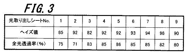
次いで、下記組成の電子輸送層用塗布液を調製し、該電子輸送層用塗布液を、1500rpm、30秒の条件でスピンコーターにより、発光層35上に塗布した。そして、電子輸送層用塗布液が塗布された素子基板31を、基板表面温度が120℃になる環境下で30分加熱乾燥し、これにより、電子輸送層36を形成した。なお、別途用意した基板上に、電子輸送層用塗布液の上記塗布条件と同じ条件で電子輸送層用塗布液を塗布して電子輸送層を形成し、その膜厚を測定したところ、膜厚は30nmであった。
Next, an electron transport layer coating solution having the following composition was prepared, and the electron transport layer coating solution was applied onto the
(電子輸送層用塗布液)
2,2,3,3−テトラフルオロ−1−プロパノール:100g
電子輸送材料(ET−A):0.75g(Coating liquid for electron transport layer)
2,2,3,3-tetrafluoro-1-propanol: 100 g
Electron transport material (ET-A): 0.75 g
なお、上記電子輸送層用塗布液に含まれる電子輸送材料(ET−A)は、カルバゾール誘導体であり、下記構造式(5)で表される。 The electron transport material (ET-A) contained in the electron transport layer coating solution is a carbazole derivative and is represented by the following structural formula (5).
次いで、電子輸送層36まで形成された素子基板31を、大気暴露せずに、蒸着機に移動させ、その後、蒸着機内を4×10⁻⁴Paまで減圧した。なお、減圧前に、予め、フッ化カリウム及びアルミニウムをそれぞれタンタル製抵抗加熱ボートに入れ、該抵抗加熱ボートを蒸着機に取り付けた。Next, the
次いで、フッ化カリウムの入った抵抗加熱ボートに通電して該抵抗加熱ボートを加熱した。これにより、電子輸送層36上に、フッ化カリウムを蒸着して、膜厚3nmの電子注入層37を形成した。
Subsequently, the resistance heating boat containing potassium fluoride was energized to heat the resistance heating boat. Thereby, potassium fluoride was vapor-deposited on the
次いで、アルミニウムの入った抵抗加熱ボートに通電して該抵抗加熱ボートを加熱した。これにより、電子注入層37上に、アルミニウムを蒸着速度1〜2nm/秒で蒸着して、膜厚100nmの陰極38を形成した。
Next, the resistance heating boat containing aluminum was energized to heat the resistance heating boat. As a result, aluminum was deposited on the
ここでは、このようにして、有機EL素子本体部30を作製した。その後、有機EL素子本体部30の陰極38側の表面に封止材を設けた。そして、最後に、素子基板31の光取り出し面(陽極32側とは反対側の面)に、上述した第1〜第8の光取り出しシートのいずれかを接着剤を介して貼り付けて、下記各種実施例及び各種比較例の有機EL素子を作製した。
Here, the organic
[実施例1]
(1)有機EL素子の構成(実施例1−1〜1−6)
実施例1では、上記第4〜第9の光取り出しシートをそれぞれ用いて有機EL素子(実施例1−1〜1−6)を作製した。[Example 1]
(1) Configuration of organic EL element (Examples 1-1 to 1-6)
In Example 1, organic EL elements (Examples 1-1 to 1-6) were produced using the fourth to ninth light extraction sheets, respectively.
また、この例では、実施例1−1〜1−6の有機EL素子と比較するため、光取り出しシートを備えない有機EL素子(比較例1−1)を作製した。さらに、比較例として、上記第1〜第3の光取り出しシートをそれぞれ用いて有機EL素子(比較例1−2〜1−4)を作製した。 Moreover, in this example, in order to compare with the organic EL element of Examples 1-1 to 1-6, an organic EL element (Comparative Example 1-1) not including a light extraction sheet was produced. Furthermore, as comparative examples, organic EL elements (Comparative Examples 1-2 to 1-4) were produced using the first to third light extraction sheets, respectively.
(2)特性評価
実施例1では、上述のようにして作製した実施例1−1〜1−6及び比較例1−1〜1−4の各有機EL素子に対して、次のような輝度特性の評価を行った。(2) Characteristic Evaluation In Example 1, the following luminance was obtained for each of the organic EL elements of Examples 1-1 to 1-6 and Comparative Examples 1-1 to 1-4 produced as described above. The characteristics were evaluated.
輝度特性の評価では、まず、作製直後の各有機EL素子に、2.5mA/cm2の直流定電流を流したときの輝度(初期輝度)を、分光放射輝度計CS−2000(コニカミノルタセンシング製)を用いて測定した。そして、この測定した輝度に基づいて、光取り出し効率を算出した。なお、光取り出し効率は、光取り出しシートを備えない有機EL素子(比較例1−1)の輝度に対する、光取り出しシートを備える有機EL素子(実施例1−1〜1−6及び比較例1−2〜1−4)の輝度の比率とした。In the evaluation of luminance characteristics, first, the luminance (initial luminance) when a DC constant current of 2.5 mA / cm 2 was passed through each organic EL element immediately after fabrication was measured using a spectral radiance meter CS-2000 (Konica Minolta Sensing). ). Then, based on the measured luminance, the light extraction efficiency was calculated. In addition, light extraction efficiency is the organic EL element (Examples 1-1 to 1-6 and Comparative Example 1- 1) provided with the light extraction sheet with respect to the luminance of the organic EL element (Comparative Example 1-1) not including the light extraction sheet. The luminance ratio was 2 to 1-4).
また、この例における輝度特性の評価では、実施例1−1〜1−6及び比較例1−1〜1−4の各有機EL素子を、温度60℃、相対湿度90%の恒湿恒温槽内で100時間放置した後、上記手法と同様にして輝度(高温高湿後輝度)を測定した(耐候性試験)。 Further, in the evaluation of the luminance characteristics in this example, each of the organic EL elements of Examples 1-1 to 1-6 and Comparative Examples 1-1 to 1-4 is a constant temperature and humidity chamber having a temperature of 60 ° C. and a relative humidity of 90%. Then, the brightness (brightness after high temperature and high humidity) was measured (weather resistance test) in the same manner as described above.
さらに、この例における輝度特性の評価では、有機EL素子を恒湿恒温槽に投入する前の輝度(初期輝度)と、投入後の輝度(高温高湿後輝度)とから輝度低下率を算出した。具体的には、[投入後の輝度/投入前の輝度]×100(%)の算出式で輝度低下率を算出した。 Further, in the evaluation of the luminance characteristics in this example, the luminance reduction rate was calculated from the luminance before the organic EL element was put into the constant temperature and humidity chamber (initial luminance) and the luminance after the addition (brightness after high temperature and high humidity). . Specifically, the luminance reduction rate was calculated using a formula of [luminance after injection / luminance before injection] × 100 (%).
また、実施例1の特性評価では、実施例1−1〜1−6及び比較例1−1〜1−4の各有機EL素子の光取り出しシートの黄変の有無を調べた。具体的には、上述した耐候性試験後、非発光状態で、有機EL素子の光取り出しシート側の面を目視で観察し、黄変の有無を2段階(後述の「OK」評価、「NG」評価)で評価した。 Moreover, in the characteristic evaluation of Example 1, the presence or absence of yellowing of the light extraction sheet | seat of each organic EL element of Examples 1-1 to 1-6 and Comparative Examples 1-1 to 1-4 was investigated. Specifically, after the weather resistance test described above, the surface of the organic EL element on the light extraction sheet side is visually observed in a non-light-emitting state, and the presence or absence of yellowing is evaluated in two stages (described later as “OK” evaluation, “NG”). "Evaluation).
図5に、上記各種評価の結果を示す。なお、図5には、評価結果だけでなく、各有機EL素子の素子基板及び光取り出しシートの構成も一緒に記載する。また、図5中の黄変の有無を示す「OK」評価及び「NG」評価の基準は下記の通りである。
OK:黄変が認識できない。
NG:明らかに黄色に変色している。FIG. 5 shows the results of the various evaluations. In FIG. 5, not only the evaluation results but also the configurations of the element substrate and the light extraction sheet of each organic EL element are described together. In addition, the criteria for “OK” evaluation and “NG” evaluation indicating the presence or absence of yellowing in FIG. 5 are as follows.
OK: Yellowing cannot be recognized.
NG: Clearly yellow.
図5に示す評価結果から明らかなように、実施例1−1〜1−6の各有機EL素子では、輝度特性の全ての項目(輝度(初期輝度)、光取り出し効率、高温高湿後輝度及び輝度低下率)において、比較例1−1〜1−4の有機EL素子の特性以上の特性が得られた。 As is apparent from the evaluation results shown in FIG. 5, in each of the organic EL elements of Examples 1-1 to 1-6, all items of luminance characteristics (luminance (initial luminance), light extraction efficiency, luminance after high temperature and high humidity) In addition, in the luminance reduction rate, characteristics higher than those of the organic EL elements of Comparative Examples 1-1 to 1-4 were obtained.
また、比較例1−2〜1−4では、黄変が見られたが、実施例1−1〜1−6では、黄変が観測されなかった。なお、光取り出しシートを備えない比較例1−1の有機EL素子では黄変は見られないが、輝度(初期輝度)、光取り出し効率及び高温高湿後輝度が他の有機EL素子に比べて劣る。 Moreover, yellowing was seen in Comparative Examples 1-2 to 1-4, but yellowing was not observed in Examples 1-1 to 1-6. In addition, although yellowing is not seen in the organic EL element of Comparative Example 1-1 that does not include the light extraction sheet, the luminance (initial luminance), the light extraction efficiency, and the luminance after high temperature and high humidity are higher than those of other organic EL elements. Inferior.
上記実施例1の評価結果から、光取り出しシートとして、第4〜第9の光取り出しシート(図5中のサンプル番号4〜9)を用いることにより、黄変が無く、かつ、輝度特性の優れた有機EL素子が得られることが分かった。すなわち、光拡散層に少なくともシリコン化合物が添加され、ヘイズ値が約90以上の値となり、かつ、全光透過率が約80%以上の値となる光取り出しシートを、有機EL素子の光取り出し面に設けることにより、光取り出し効率及び耐光性の両方が優れた有機EL素子が得られることが分かった。
From the evaluation results of Example 1 above, by using the fourth to ninth light extraction sheets (
[実施例2]
(1)有機EL素子の構成(実施例2−1〜2−6)
実施例2では、素子基板31の形成材料を種々変化させて有機EL素子(実施例2−1〜2−6)を作製した。なお、実施例2の有機EL素子において、素子基板31以外の構成は、上記実施例1−5の有機EL素子の対応する構成と同様とした。すなわち、実施例2では、光取り出しシートとして、光取り出し面に凹凸パターンを形成した第8の光取り出しシート(光取り出しシートのサンプル番号8)を用いた。[Example 2]
(1) Configuration of organic EL element (Examples 2-1 to 2-6)
In Example 2, organic EL elements (Examples 2-1 to 2-6) were manufactured by changing the formation material of the
実施例2−1〜2−6のそれぞれで用いた素子基板31は次の通りである。実施例2−1の有機EL素子では、素子基板31として、厚さ200μmのPEN(ポリエチレンナフタレート)フィルムを用いた。実施例2−2の有機EL素子では、素子基板31として、厚さ200μmのPET(ポリエチレンテレフタレート)フィルムを用いた。実施例2−3の有機EL素子では、素子基板31として、厚さ200μmのポリイミドフィルムを用いた。
The
また、実施例2−4の有機EL素子では、素子基板31として、厚さ0.4mmのガラス基板、すなわち、薄膜ガラスを用いた。実施例2−5の有機EL素子では、素子基板31として、厚さ0.2mmのガラス基板(薄膜ガラス)を用いた。そして、実施例2−6の有機EL素子では、素子基板31として、厚さ90μmのアルミニウム箔の両面に、厚さ30μmのポリイミド層(絶縁層)を設けたメタルフォイル基板を用いた。
Further, in the organic EL element of Example 2-4, a glass substrate having a thickness of 0.4 mm, that is, a thin film glass was used as the
なお、この例では比較のため、上記比較例1−1の有機EL素子(光取り出しシート無し)の素子基板を、厚さ200μmのPENフィルムに変更した有機EL素子(比較例2−1)を作製した。また、比較例2−1の有機EL素子の光取り出し面に上記第1の光取り出しシート(光取り出しシートのサンプル番号1)を貼り付けた有機EL素子(比較例2−2)も作製した。さらに、比較例2−1の有機EL素子において素子基板を、厚さ200μmのPETフィルムに変更した有機EL素子(比較例2−3)を作製した。
In this example, for comparison, an organic EL element (Comparative Example 2-1) in which the element substrate of the organic EL element (without light extraction sheet) of Comparative Example 1-1 was changed to a PEN film having a thickness of 200 μm was used. Produced. Moreover, the organic EL element (Comparative Example 2-2) which affixed the said 1st light extraction sheet | seat (
(2)特性評価
実施例2では、上記実施例2−1〜2−6及び比較例2−1〜2−3の各有機EL素子に対して、上記実施例1と同様にして、輝度特性、及び、黄変の有無を評価した。なお、黄変の有無の評価基準は、上記実施例1の評価基準と同様である。(2) Characteristic Evaluation In Example 2, the luminance characteristics of each of the organic EL elements in Examples 2-1 to 2-6 and Comparative Examples 2-1 to 2-3 were the same as in Example 1. The presence or absence of yellowing was evaluated. In addition, the evaluation criteria of the presence or absence of yellowing are the same as the evaluation criteria of the said Example 1.
また、この例では、各サンプルの光取り出し効率を、次のようにして算出した。比較例2−1及び2−2のサンプルについては、比較例2−1の輝度(=550)を基準(光取り出し効率=1.00)にして光取り出し効率を求めた。実施例2−1〜2−6、及び、比較例2−3の各サンプルについては、ここでは説明を省略するが、サンプル毎(素子基板毎)に対応する、光取り出しシートを設けない構成の有機EL素子をそれぞれ作製し、該作製した光取り出しシート無しの有機EL素子の輝度を基準にして、各サンプルの光取り出し効率を求めた。 In this example, the light extraction efficiency of each sample was calculated as follows. For the samples of Comparative Examples 2-1 and 2-2, the light extraction efficiency was obtained using the luminance (= 550) of Comparative Example 2-1 as a reference (light extraction efficiency = 1.00). About each sample of Examples 2-1 to 2-6 and Comparative Example 2-3, although description is abbreviate | omitted here, the light extraction sheet | seat corresponding to every sample (each element substrate) is not provided. Each organic EL element was produced, and the light extraction efficiency of each sample was determined based on the luminance of the produced organic EL element without the light extraction sheet.
図6に、その評価結果を示す。なお、図6には、上記実施例1−5の有機EL素子の評価結果も一緒に記載する。 FIG. 6 shows the evaluation results. In addition, in FIG. 6, the evaluation result of the organic EL element of the said Example 1-5 is also described together.
図6から明らかなように、光拡散層に少なくともシリコン化合物が添加され、ヘイズ値が約90以上の値であり、かつ、全光透過率が約80%以上の値である光取り出しシートを用いた場合、素子基板31の形成材料としてPEN、PET、ポリイミド、ガラス及びメタフォイルのいずれを用いても、黄変が無く、かつ、輝度特性の優れた有機EL素子が得られることが分かった。さらに、上記構成条件を満たす光取り出しシートを用い、素子基板31としてガラス基板を用いた場合には、素子基板31(ガラス基板)の厚さに関係なく、優れた発光特性が得られることが分かった。
As is apparent from FIG. 6, a light extraction sheet in which at least a silicon compound is added to the light diffusion layer, the haze value is about 90 or more, and the total light transmittance is about 80% or more is used. In this case, it was found that even when any of PEN, PET, polyimide, glass, and metafoil was used as the material for forming the
[実施例3]
実施例3では、上記実施例1−5、上記実施例2−1〜2−6、及び、比較例2−1〜2−3の各有機EL素子に対して、JIS C8105−1に記載の手法に従ってグローワイヤー耐熱性試験を実施し、各有機EL素子の難燃性について調べた。[Example 3]
In Example 3, the organic EL elements of Examples 1-5, Examples 2-1 to 2-6, and Comparative Examples 2-1 to 2-3 are described in JIS C8105-1. A glow wire heat resistance test was conducted according to the method, and the flame retardancy of each organic EL element was examined.
図7に、その評価結果を示す。なお、図7に示す難燃性の「OK」評価及び「NG」評価の基準は下記の通りである。
OK:グローワイヤーを有機EL素子から離した後、30秒より短い時間で消火した。
NG:グローワイヤーを有機EL素子から離した後、30秒を越えても消火しない。FIG. 7 shows the evaluation results. In addition, the flame retardant “OK” evaluation and “NG” evaluation criteria shown in FIG. 7 are as follows.
OK: After the glow wire was separated from the organic EL element, the fire was extinguished in a time shorter than 30 seconds.
NG: The fire wire is not extinguished even after 30 seconds after the glow wire is separated from the organic EL element.
図7から明らかなように、光拡散層に少なくともシリコン化合物が添加され、ヘイズ値が約90以上の値となり、かつ、全光透過率が約80%以上の値となる光取り出しシートを用いた場合、光取り出し効率及び耐候性だけでなく、難燃性にも優れた有機EL素子が得られることが分かった。 As is clear from FIG. 7, a light extraction sheet was used in which at least a silicon compound was added to the light diffusion layer, the haze value was about 90 or more, and the total light transmittance was about 80% or more. In this case, it was found that an organic EL element excellent in not only light extraction efficiency and weather resistance but also flame retardancy can be obtained.
なお、上記各種実施例では、具体的に示さなかったが、光取り出しシートの基材をフッ素樹脂含有フィルムで構成した場合についても、上記各種実施例と同様の評価を行った。その結果、光取り出しシートの基材をフッ素樹脂含有フィルムで構成した場合もまた、上記各種実施例と同様の評価結果が得られた。 In addition, although it did not show concretely in the said various Examples, also when the base material of the light extraction sheet | seat was comprised with the fluororesin containing film, evaluation similar to the said various Examples was performed. As a result, when the base material of the light extraction sheet was composed of a fluororesin-containing film, the same evaluation results as in the above various examples were obtained.
1…有機EL素子本体部、2…光取り出しシート、2a…基材、2b…光拡散層、3…封止材、10…有機EL素子、11…素子基板、12…陽極、13…有機化合物層、14…陰極、20…面状発光体、21…支持基板、22…接着部材
DESCRIPTION OF
Claims (9)
前記有機エレクトロルミネッセンス素子本体部の光取り出し側に設けられた光取り出しシートとを備え、
前記光取り出しシートがシリコン化合物及び臭素含有化合物を含み、前記光取り出しシートのヘイズ値が90以上の値であり、かつ、前記光取り出しシートの全光透過率が80%以上の値であることを特徴とする
有機エレクトロルミネッセンス素子。 An organic substrate having an element substrate, a first electrode formed on the element substrate, an organic compound layer formed on the first electrode and including a light emitting layer, and a second electrode formed on the organic compound layer A luminescence element body,
A light extraction sheet provided on the light extraction side of the organic electroluminescence element body, and
The light extraction sheet contains a silicon compound and a bromine-containing compound, the haze value of the light extraction sheet is a value of 90 or more, and the total light transmittance of the light extraction sheet is a value of 80% or more. An organic electroluminescence device characterized.
請求項1に記載の有機エレクトロルミネッセンス素子。 2. The organic electroluminescence element according to claim 1, wherein the light extraction sheet has a haze value of 92 or more and a total light transmittance of the light extraction sheet is 82% or more.
請求項1又は2に記載の有機エレクトロルミネッセンス素子。 The light extraction sheet has a base material, and the base material is any one of a polycarbonate film, a polyethylene terephthalate film, a polyethylene naphthalate film, a polyimide film, and a fluororesin-containing film. Or the organic electroluminescent element of 2.
請求項1〜3のいずれか一項に記載の有機エレクトロルミネッセンス素子。 The organic light-emitting device according to any one of claims 1 to 3, wherein the light extraction sheet further contains a polyacrylate resin.
請求項1〜4のいずれか一項に記載の有機エレクトロルミネッセンス素子。 The organic electroluminescence element according to claim 1, wherein a predetermined uneven pattern is formed on a light extraction surface of the light extraction sheet.
請求項1〜5のいずれか一項に記載の有機エレクトロルミネッセンス素子。 The organic electroluminescence element according to claim 1 , wherein the element substrate is a thin film glass .
請求項1〜5のいずれか一項に記載の有機エレクトロルミネッセンス素子。 The element substrate, an organic electroluminescent device according to any one of claims 1 to 5, characterized in that a metal foil.
請求項1〜5のいずれか一項に記載の有機エレクトロルミネッセンス素子。 The element substrate, the organic electroluminescence device according to any one of claims 1-5, characterized in that a polyimide film.
前記複数の有機エレクトロルミネッセンス素子を、所定の形態で配列して支持する支持部材とを備え、A support member for arranging and supporting the plurality of organic electroluminescence elements in a predetermined form;
前記有機エレクトロルミネッセンス素子が、素子基板、該素子基板上に形成された第1電極、該第1電極上に形成されかつ発光層を含む有機化合物層、及び、該有機化合物層上に形成された第2電極を有する有機エレクトロルミネッセンス素子本体部と、該有機エレクトロルミネッセンス素子本体部の光取り出し側に設けられた光取り出しシートとを有し、The organic electroluminescence element is formed on an element substrate, a first electrode formed on the element substrate, an organic compound layer formed on the first electrode and including a light emitting layer, and the organic compound layer An organic electroluminescence element body having a second electrode, and a light extraction sheet provided on the light extraction side of the organic electroluminescence element body,
前記光取り出しシートがシリコン化合物及び臭素含有化合物を含み、前記光取り出しシートのヘイズ値が90以上の値であり、かつ、前記光取り出しシートの全光透過率が80%以上の値であることを特徴とするThe light extraction sheet contains a silicon compound and a bromine-containing compound, the haze value of the light extraction sheet is a value of 90 or more, and the total light transmittance of the light extraction sheet is a value of 80% or more. Characterize
面状発光体。Planar light emitter.
Applications Claiming Priority (3)
| Application Number | Priority Date | Filing Date | Title |
|---|---|---|---|
| JP2011248367 | 2011-11-14 | ||
| JP2011248367 | 2011-11-14 | ||
| PCT/JP2012/075690 WO2013073301A1 (en) | 2011-11-14 | 2012-10-03 | Organic electroluminescence element and planar light-emitting body |
Publications (2)
| Publication Number | Publication Date |
|---|---|
| JPWO2013073301A1 JPWO2013073301A1 (en) | 2015-04-02 |
| JP6052182B2 true JP6052182B2 (en) | 2016-12-27 |
Family
ID=48429371
Family Applications (1)
| Application Number | Title | Priority Date | Filing Date |
|---|---|---|---|
| JP2013544176A Expired - Fee Related JP6052182B2 (en) | 2011-11-14 | 2012-10-03 | Organic electroluminescence device and planar light emitter |
Country Status (4)
| Country | Link |
|---|---|
| US (1) | US9627653B2 (en) |
| EP (1) | EP2782417A4 (en) |
| JP (1) | JP6052182B2 (en) |
| WO (1) | WO2013073301A1 (en) |
Families Citing this family (11)
| Publication number | Priority date | Publication date | Assignee | Title |
|---|---|---|---|---|
| WO2014042056A1 (en) * | 2012-09-11 | 2014-03-20 | コニカミノルタ株式会社 | Organic electroluminescence element, and light extraction sheet for organic electroluminescence element |
| US9595684B2 (en) * | 2012-11-30 | 2017-03-14 | Lg Chem, Ltd. | Substrate for organic electronic device having high refractive layer on light scattering, optical functional layer |
| CN105325056B (en) * | 2013-06-18 | 2017-09-08 | 柯尼卡美能达株式会社 | Organic Light Emitting Components |
| KR102073791B1 (en) * | 2013-09-03 | 2020-02-05 | 삼성전자주식회사 | Flexible electric device and method of manufacturing the same |
| JP6438678B2 (en) | 2014-05-14 | 2018-12-19 | Jxtgエネルギー株式会社 | Film member having an uneven structure |
| CN111263483B (en) | 2015-02-25 | 2023-04-07 | 日本先锋公司 | Light emitting device, method for manufacturing light emitting device, and light emitting system |
| CN104934550A (en) * | 2015-05-07 | 2015-09-23 | 京东方科技集团股份有限公司 | OLED device packaging structure, packaging method and electronic device |
| KR20170050729A (en) * | 2015-10-30 | 2017-05-11 | 엘지디스플레이 주식회사 | Organic light emitting display device |
| CN107123754A (en) * | 2017-06-14 | 2017-09-01 | 京东方科技集团股份有限公司 | A kind of organic electroluminescence device and preparation method, evaporated device |
| JP7257100B2 (en) * | 2017-09-11 | 2023-04-13 | 東洋製罐グループホールディングス株式会社 | Transparent substrate, thin film supporting substrate |
| JP7323988B2 (en) * | 2018-03-27 | 2023-08-09 | 株式会社ダイセル | Organic EL display device |
Family Cites Families (120)
| Publication number | Priority date | Publication date | Assignee | Title |
|---|---|---|---|---|
| JP2525209B2 (en) | 1987-09-30 | 1996-08-14 | 油谷重工株式会社 | Support device for vibration reduction |
| US5061569A (en) | 1990-07-26 | 1991-10-29 | Eastman Kodak Company | Electroluminescent device with organic electroluminescent medium |
| JPH04297076A (en) | 1991-01-31 | 1992-10-21 | Toshiba Corp | Organic el element |
| JP3016896B2 (en) | 1991-04-08 | 2000-03-06 | パイオニア株式会社 | Organic electroluminescence device |
| JP3048702B2 (en) | 1991-09-13 | 2000-06-05 | 鐘淵化学工業株式会社 | Polyamic acid copolymer, polyimide copolymer, polyimide film and methods for producing them |
| JPH06325871A (en) | 1993-05-18 | 1994-11-25 | Mitsubishi Kasei Corp | Organic electroluminescent element |
| JP3561549B2 (en) | 1995-04-07 | 2004-09-02 | 三洋電機株式会社 | Organic electroluminescence device |
| JP3529543B2 (en) | 1995-04-27 | 2004-05-24 | パイオニア株式会社 | Organic electroluminescence device |
| US5719467A (en) | 1995-07-27 | 1998-02-17 | Hewlett-Packard Company | Organic electroluminescent device |
| JP3645642B2 (en) | 1996-03-25 | 2005-05-11 | Tdk株式会社 | Organic electroluminescence device |
| US5776622A (en) | 1996-07-29 | 1998-07-07 | Eastman Kodak Company | Bilayer eletron-injeting electrode for use in an electroluminescent device |
| JP4486713B2 (en) | 1997-01-27 | 2010-06-23 | 淳二 城戸 | Organic electroluminescent device |
| JP3852509B2 (en) | 1998-01-09 | 2006-11-29 | ソニー株式会社 | Electroluminescent device and manufacturing method thereof |
| JPH11204359A (en) | 1998-01-14 | 1999-07-30 | Tokin Corp | Method and device for manufacturing dust core |
| JPH11251067A (en) | 1998-03-02 | 1999-09-17 | Junji Kido | Organic electroluminescent device |
| US6097147A (en) | 1998-09-14 | 2000-08-01 | The Trustees Of Princeton University | Structure for high efficiency electroluminescent device |
| GB9820805D0 (en) | 1998-09-25 | 1998-11-18 | Isis Innovation | Divalent lanthanide metal complexes |
| JP2000119419A (en) | 1998-10-16 | 2000-04-25 | Du Pont Toray Co Ltd | Copolymerized polyimide film, method for producing the same, and metal wiring circuit board using the same as a base material |
| JP2000196140A (en) | 1998-12-28 | 2000-07-14 | Sharp Corp | Organic electroluminescent device and manufacturing method thereof |
| BRPI0009215B1 (en) | 1999-03-23 | 2017-05-09 | Univ Southern California | cyclometallized metal complexes as phosphorescent dopants in organic light-emitting diodes |
| JP2000298203A (en) * | 1999-04-15 | 2000-10-24 | Shiseido Co Ltd | Optical diffusion plate, illuminating device and liquid crystal display device using the same |
| EP1729327B2 (en) | 1999-05-13 | 2022-08-10 | The Trustees Of Princeton University | Use of a phosphorescent iridium compound as emissive molecule in an organic light emitting device |
| EP1645328A1 (en) * | 1999-08-25 | 2006-04-12 | Diamond Innovations, Inc. | High pressure/high temperature production of colored diamonds |
| JP4729154B2 (en) | 1999-09-29 | 2011-07-20 | 淳二 城戸 | Organic electroluminescent device, organic electroluminescent device group, and method for controlling emission spectrum thereof |
| JP2001181617A (en) | 1999-12-27 | 2001-07-03 | Fuji Photo Film Co Ltd | Light emitting element material composed of orthometalated palladium complex and light emitting element |
| JP2001181616A (en) | 1999-12-27 | 2001-07-03 | Fuji Photo Film Co Ltd | Light emitting element material composed of orthometalated palladium complex and light emitting element |
| JP3929689B2 (en) | 2000-03-28 | 2007-06-13 | 富士フイルム株式会社 | Highly efficient red light emitting device, light emitting device material comprising iridium complex and novel iridium complex |
| JP3929690B2 (en) | 1999-12-27 | 2007-06-13 | 富士フイルム株式会社 | Light emitting device material, light emitting device and novel iridium complex comprising orthometalated iridium complex |
| JP3929706B2 (en) | 2000-02-10 | 2007-06-13 | 富士フイルム株式会社 | Light emitting device material and light emitting device comprising iridium complex |
| JP4890669B2 (en) | 2000-03-13 | 2012-03-07 | Tdk株式会社 | Organic EL device |
| JP2002008860A (en) | 2000-04-18 | 2002-01-11 | Mitsubishi Chemicals Corp | Organic electroluminescent device |
| JP2002015871A (en) | 2000-04-27 | 2002-01-18 | Toray Ind Inc | Light emitting element |
| JP2001313178A (en) | 2000-04-28 | 2001-11-09 | Pioneer Electronic Corp | Organic electroluminescence device |
| JP2001313179A (en) | 2000-05-01 | 2001-11-09 | Mitsubishi Chemicals Corp | Organic electroluminescent device |
| JP4382961B2 (en) | 2000-05-02 | 2009-12-16 | 富士フイルム株式会社 | Light emitting element |
| JP4048521B2 (en) | 2000-05-02 | 2008-02-20 | 富士フイルム株式会社 | Light emitting element |
| JP4683766B2 (en) | 2000-05-22 | 2011-05-18 | 株式会社半導体エネルギー研究所 | Active matrix light emitting device |
| JP5062797B2 (en) | 2000-05-22 | 2012-10-31 | 昭和電工株式会社 | Organic electroluminescence device and light emitting material |
| JP2002062824A (en) | 2000-06-05 | 2002-02-28 | Semiconductor Energy Lab Co Ltd | Light emitting device |
| JP4290858B2 (en) | 2000-06-12 | 2009-07-08 | 富士フイルム株式会社 | Organic electroluminescence device |
| JP2002083684A (en) | 2000-06-23 | 2002-03-22 | Semiconductor Energy Lab Co Ltd | Light-emitting device |
| JP4340401B2 (en) | 2000-07-17 | 2009-10-07 | 富士フイルム株式会社 | Light emitting device and iridium complex |
| JP4712232B2 (en) | 2000-07-17 | 2011-06-29 | 富士フイルム株式会社 | Light emitting device and azole compound |
| JP2002043056A (en) | 2000-07-19 | 2002-02-08 | Canon Inc | Light emitting element |
| EP1325671B1 (en) | 2000-08-11 | 2012-10-24 | The Trustees Of Princeton University | Organometallic compounds and emission-shifting organic electrophosphorescence |
| JP2002141173A (en) | 2000-08-22 | 2002-05-17 | Semiconductor Energy Lab Co Ltd | Light emitting device |
| JP4344494B2 (en) | 2000-08-24 | 2009-10-14 | 富士フイルム株式会社 | Light emitting device and novel polymer element |
| JP4554047B2 (en) | 2000-08-29 | 2010-09-29 | 株式会社半導体エネルギー研究所 | Light emitting device |
| JP4505162B2 (en) | 2000-09-21 | 2010-07-21 | 富士フイルム株式会社 | Light emitting device and novel rhenium complex |
| JP4067286B2 (en) | 2000-09-21 | 2008-03-26 | 富士フイルム株式会社 | Light emitting device and iridium complex |
| JP4454130B2 (en) | 2000-09-25 | 2010-04-21 | 京セラ株式会社 | Organic electroluminescence device |
| JP4154140B2 (en) | 2000-09-26 | 2008-09-24 | キヤノン株式会社 | Metal coordination compounds |
| JP2002184582A (en) | 2000-09-28 | 2002-06-28 | Semiconductor Energy Lab Co Ltd | Luminescent device |
| JP4026740B2 (en) | 2000-09-29 | 2007-12-26 | 富士フイルム株式会社 | Organic light emitting device material and organic light emitting device using the same |
| JP4092901B2 (en) | 2000-10-30 | 2008-05-28 | 株式会社豊田中央研究所 | Organic electroluminescence device |
| JP4086498B2 (en) | 2000-11-29 | 2008-05-14 | キヤノン株式会社 | Metal coordination compound, light emitting device and display device |
| JP4086499B2 (en) | 2000-11-29 | 2008-05-14 | キヤノン株式会社 | Metal coordination compound, light emitting device and display device |
| JP3855675B2 (en) | 2000-11-30 | 2006-12-13 | 三菱化学株式会社 | Organic electroluminescence device |
| JP2002255934A (en) | 2000-12-25 | 2002-09-11 | Fuji Photo Film Co Ltd | New compound, its polymer, light emission element material using these substances and the light emission element |
| JP4048525B2 (en) | 2000-12-25 | 2008-02-20 | 富士フイルム株式会社 | Novel indole derivative and light emitting device using the same |
| JP2002203678A (en) | 2000-12-27 | 2002-07-19 | Fuji Photo Film Co Ltd | Light-emitting element |
| JP2002203679A (en) | 2000-12-27 | 2002-07-19 | Fuji Photo Film Co Ltd | Light-emitting element |
| JP4153694B2 (en) | 2000-12-28 | 2008-09-24 | 株式会社東芝 | Organic EL device and display device |
| US6720090B2 (en) | 2001-01-02 | 2004-04-13 | Eastman Kodak Company | Organic light emitting diode devices with improved luminance efficiency |
| JP4598282B2 (en) | 2001-02-09 | 2010-12-15 | 三井化学株式会社 | Amine compound and organic electroluminescent device containing the compound |
| JP3988915B2 (en) | 2001-02-09 | 2007-10-10 | 富士フイルム株式会社 | Transition metal complex, light emitting device material comprising the same, and light emitting device |
| JP4215145B2 (en) | 2001-02-21 | 2009-01-28 | 富士フイルム株式会社 | Light emitting device material and light emitting device |
| US7026480B2 (en) | 2001-03-08 | 2006-04-11 | The University Of Hong Kong | Organometallic light-emitting material |
| JP4307000B2 (en) | 2001-03-08 | 2009-08-05 | キヤノン株式会社 | Metal coordination compound, electroluminescent element and display device |
| JP4438042B2 (en) | 2001-03-08 | 2010-03-24 | キヤノン株式会社 | Metal coordination compound, electroluminescent element and display device |
| JP2002334788A (en) | 2001-03-09 | 2002-11-22 | Sony Corp | Organic electroluminescent device |
| JP2002334787A (en) | 2001-03-09 | 2002-11-22 | Sony Corp | Organic electroluminescent device |
| JP4655410B2 (en) | 2001-03-09 | 2011-03-23 | ソニー株式会社 | Organic electroluminescence device |
| JP2002334786A (en) | 2001-03-09 | 2002-11-22 | Sony Corp | Organic electroluminescent device |
| JP2002343572A (en) | 2001-03-14 | 2002-11-29 | Canon Inc | Light-emitting element and display device using porphyrin derivative compound |
| JP4307001B2 (en) | 2001-03-14 | 2009-08-05 | キヤノン株式会社 | Metal coordination compound, electroluminescent element and display device |
| JP4169246B2 (en) | 2001-03-16 | 2008-10-22 | 富士フイルム株式会社 | Heterocyclic compound and light emitting device using the same |
| JP2002280178A (en) | 2001-03-16 | 2002-09-27 | Canon Inc | Organic light emitting device |
| JP2002280180A (en) | 2001-03-16 | 2002-09-27 | Canon Inc | Organic light emitting device |
| JP2002280179A (en) | 2001-03-16 | 2002-09-27 | Canon Inc | Organic light emitting device |
| JP3964245B2 (en) | 2001-03-28 | 2007-08-22 | 株式会社半導体エネルギー研究所 | ORGANIC LIGHT EMITTING ELEMENT AND LIGHT EMITTING DEVICE USING THE ELEMENT |
| JP2002299060A (en) | 2001-03-30 | 2002-10-11 | Fuji Photo Film Co Ltd | Organic light emitting device |
| JP2002302516A (en) | 2001-04-03 | 2002-10-18 | Fuji Photo Film Co Ltd | New polymer and light emitting device using the same |
| JP2002363227A (en) | 2001-04-03 | 2002-12-18 | Fuji Photo Film Co Ltd | New polymer and light emitting device using the same |
| JP2002305083A (en) | 2001-04-04 | 2002-10-18 | Mitsubishi Chemicals Corp | Organic electroluminescent device |
| JP2002308837A (en) | 2001-04-05 | 2002-10-23 | Fuji Photo Film Co Ltd | Novel compound and light emitting device using the same |
| JP2002308855A (en) | 2001-04-05 | 2002-10-23 | Fuji Photo Film Co Ltd | Novel compound and light emitting device using the same |
| JP2003007471A (en) | 2001-04-13 | 2003-01-10 | Semiconductor Energy Lab Co Ltd | Organic light emitting element and light emitting device using the element |
| JP2002324679A (en) | 2001-04-26 | 2002-11-08 | Honda Motor Co Ltd | Organic electroluminescence device |
| JP2002343568A (en) | 2001-05-10 | 2002-11-29 | Sony Corp | Organic electroluminescent device |
| JP2002352957A (en) | 2001-05-23 | 2002-12-06 | Honda Motor Co Ltd | Organic electroluminescence device |
| JP2002352960A (en) | 2001-05-29 | 2002-12-06 | Hitachi Ltd | Thin film electroluminescent device |
| JP2003007469A (en) | 2001-06-25 | 2003-01-10 | Canon Inc | Light emitting element and display device |
| JP4628594B2 (en) | 2001-06-25 | 2011-02-09 | 昭和電工株式会社 | Organic light emitting device and light emitting material |
| JP4003824B2 (en) | 2001-07-11 | 2007-11-07 | 富士フイルム株式会社 | Light emitting element |
| JP4789359B2 (en) | 2001-07-11 | 2011-10-12 | 株式会社半導体エネルギー研究所 | Light emitting device |
| JP2003109747A (en) * | 2001-07-24 | 2003-04-11 | Matsushita Electric Works Ltd | Organic electroluminescent surface light emitter and liquid crystal display |
| JP4433680B2 (en) | 2002-06-10 | 2010-03-17 | コニカミノルタホールディングス株式会社 | Thin film formation method |
| JP3962997B2 (en) | 2003-08-01 | 2007-08-22 | 荒川化学工業株式会社 | Alkoxy group-containing silane-modified block copolymer type polyamic acid, block copolymerized polyimide-silica hybrid cured product, and metal laminate |
| JP4074847B2 (en) * | 2003-09-30 | 2008-04-16 | 恵和株式会社 | Optical sheet and backlight unit using the same |
| US20060257678A1 (en) * | 2005-05-10 | 2006-11-16 | Benson Olester Jr | Fiber reinforced optical films |
| JP2007056198A (en) | 2005-08-26 | 2007-03-08 | Teijin Ltd | Polyimide film and process for producing the same |
| KR20080055840A (en) * | 2005-09-15 | 2008-06-19 | 니폰 제온 가부시키가이샤 | Direct type backlight device |
| JP2007206569A (en) * | 2006-02-03 | 2007-08-16 | Daicel Chem Ind Ltd | Optical sheet |
| US20080008845A1 (en) * | 2006-07-07 | 2008-01-10 | Young Oh | Light diffusion sheet for a display device |
| US20090214828A1 (en) | 2008-02-26 | 2009-08-27 | Vicki Herzl Watkins | Blunt tip prism film and methods for making the same |
| JP2009238694A (en) | 2008-03-28 | 2009-10-15 | Sumitomo Chemical Co Ltd | Organic electroluminescent element and its manufacturing method |
| US7957621B2 (en) * | 2008-12-17 | 2011-06-07 | 3M Innovative Properties Company | Light extraction film with nanoparticle coatings |
| US20120080710A1 (en) * | 2009-06-11 | 2012-04-05 | Hiroyasu Inoue | Surface light source device, lighting device, and backlight device |
| JP2011018583A (en) | 2009-07-09 | 2011-01-27 | Fujifilm Corp | Organic el device and its design method |
| WO2011046144A1 (en) * | 2009-10-14 | 2011-04-21 | 日本ゼオン株式会社 | Organic electroluminescent light source device |
| EP2490506A1 (en) * | 2009-10-15 | 2012-08-22 | Asahi Glass Company, Limited | Organic led element, glass frit for diffusion layer for use in organic led element, and method for production of diffusion layer for use in organic led element |
| US10581020B2 (en) * | 2011-02-08 | 2020-03-03 | Vitro Flat Glass Llc | Light extracting substrate for organic light emitting diode |
| JP5731830B2 (en) * | 2010-01-19 | 2015-06-10 | パナソニック株式会社 | Planar light emitting device |
| JP5960047B2 (en) * | 2010-02-23 | 2016-08-02 | コニカミノルタ株式会社 | Organic electroluminescence device and method for manufacturing the same |
| US9541681B2 (en) | 2010-05-26 | 2017-01-10 | Konica Minolta Holdings, Inc. | Light extraction sheet, organic electroluminescence element and illumination device |
| JP2011248104A (en) * | 2010-05-27 | 2011-12-08 | Jsr Corp | Light extraction film and manufacturing method of the same |
| EP2518789B1 (en) * | 2011-04-18 | 2016-04-13 | Corning Precision Materials Co., Ltd. | Method of manufacturing a light extraction substrate for an electroluminescent device |
| JPWO2013035299A1 (en) * | 2011-09-07 | 2015-03-23 | パナソニックIpマネジメント株式会社 | Light emitting device and light sheet |
| KR101892711B1 (en) * | 2011-12-28 | 2018-08-29 | 삼성디스플레이 주식회사 | Organic light emitting display apparatus and the method for manufacturing the same |
-
2012
- 2012-10-03 WO PCT/JP2012/075690 patent/WO2013073301A1/en not_active Ceased
- 2012-10-03 JP JP2013544176A patent/JP6052182B2/en not_active Expired - Fee Related
- 2012-10-03 EP EP12849338.4A patent/EP2782417A4/en not_active Withdrawn
- 2012-10-03 US US14/355,055 patent/US9627653B2/en active Active
Also Published As
| Publication number | Publication date |
|---|---|
| US9627653B2 (en) | 2017-04-18 |
| EP2782417A1 (en) | 2014-09-24 |
| JPWO2013073301A1 (en) | 2015-04-02 |
| WO2013073301A1 (en) | 2013-05-23 |
| US20140264317A1 (en) | 2014-09-18 |
| EP2782417A4 (en) | 2015-08-05 |
Similar Documents
| Publication | Publication Date | Title |
|---|---|---|
| JP6052182B2 (en) | Organic electroluminescence device and planar light emitter | |
| JP5835216B2 (en) | Light extraction sheet, organic electroluminescence element and lighting device | |
| JP5413459B2 (en) | White light emitting organic electroluminescence device | |
| JP6362330B2 (en) | Organic electroluminescence device and planar light emitter | |
| JP5888095B2 (en) | Organic electroluminescence device | |
| WO2013042533A1 (en) | Organic electroluminescent panel and method for producing organic electroluminescent panel | |
| JPWO2011132550A1 (en) | Organic electroluminescence element, display device and lighting device | |
| JP5678891B2 (en) | Decorative luminous body manufacturing method | |
| JP5589852B2 (en) | Organic electroluminescence device and method for manufacturing the same | |
| WO2012172883A1 (en) | Method for manufacturing organic electroluminescent element | |
| JP5879737B2 (en) | Method for manufacturing organic electroluminescence element | |
| JP5660125B2 (en) | ORGANIC ELECTROLUMINESCENT MEMBER AND METHOD FOR PRODUCING ORGANIC ELECTROLUMINESCENT ELEMENT | |
| JP2009252944A (en) | Organic electroluminescence element and its manufacturing method | |
| JP6119606B2 (en) | Organic electroluminescence panel and method for manufacturing organic electroluminescence panel | |
| JP6061450B2 (en) | ORGANIC ELECTROLUMINESCENT ELEMENT AND METHOD FOR PRODUCING ORGANIC ELECTROLUMINESCENT ELEMENT | |
| JP5428162B2 (en) | Organic electroluminescence device | |
| JP2010177338A (en) | Organic electroluminescent element, and method of manufacturing the same | |
| WO2012063656A1 (en) | Process for producing organic electroluminescent element | |
| JP4978034B2 (en) | Organic electroluminescence device | |
| JP5594291B2 (en) | Organic electroluminescence device and method for manufacturing the same | |
| JPWO2010084816A1 (en) | Organic electroluminescence device and method for manufacturing the same | |
| JP5286637B2 (en) | Organic electroluminescent panel manufacturing method, organic electroluminescent panel | |
| JP2010199021A (en) | Method of manufacturing organic electroluminescent element | |
| JP2011222385A (en) | Organic electroluminescent element manufacturing method and organic electroluminescent element | |
| JP2012234972A (en) | Organic electroluminescent element and method for manufacturing the same |
Legal Events
| Date | Code | Title | Description |
|---|---|---|---|
| A621 | Written request for application examination |
Free format text: JAPANESE INTERMEDIATE CODE: A621 Effective date: 20150519 |
|
| A131 | Notification of reasons for refusal |
Free format text: JAPANESE INTERMEDIATE CODE: A131 Effective date: 20160517 |
|
| A521 | Request for written amendment filed |
Free format text: JAPANESE INTERMEDIATE CODE: A523 Effective date: 20160706 |
|
| TRDD | Decision of grant or rejection written | ||
| A01 | Written decision to grant a patent or to grant a registration (utility model) |
Free format text: JAPANESE INTERMEDIATE CODE: A01 Effective date: 20161101 |
|
| A61 | First payment of annual fees (during grant procedure) |
Free format text: JAPANESE INTERMEDIATE CODE: A61 Effective date: 20161114 |
|
| R150 | Certificate of patent or registration of utility model |
Ref document number: 6052182 Country of ref document: JP Free format text: JAPANESE INTERMEDIATE CODE: R150 |
|
| LAPS | Cancellation because of no payment of annual fees |