JP5947904B2 - Stub minimization for multi-die wirebond assemblies with orthogonal windows - Google Patents
Stub minimization for multi-die wirebond assemblies with orthogonal windows Download PDFInfo
- Publication number
- JP5947904B2 JP5947904B2 JP2014534530A JP2014534530A JP5947904B2 JP 5947904 B2 JP5947904 B2 JP 5947904B2 JP 2014534530 A JP2014534530 A JP 2014534530A JP 2014534530 A JP2014534530 A JP 2014534530A JP 5947904 B2 JP5947904 B2 JP 5947904B2
- Authority
- JP
- Japan
- Prior art keywords
- terminal
- microelectronic
- terminals
- package
- grid
- Prior art date
- Legal status (The legal status is an assumption and is not a legal conclusion. Google has not performed a legal analysis and makes no representation as to the accuracy of the status listed.)
- Expired - Fee Related
Links
Images


Classifications
-
- G—PHYSICS
- G11—INFORMATION STORAGE
- G11C—STATIC STORES
- G11C5/00—Details of stores covered by group G11C11/00
- G11C5/02—Disposition of storage elements, e.g. in the form of a matrix array
-
- G—PHYSICS
- G11—INFORMATION STORAGE
- G11C—STATIC STORES
- G11C5/00—Details of stores covered by group G11C11/00
- G11C5/02—Disposition of storage elements, e.g. in the form of a matrix array
- G11C5/04—Supports for storage elements, e.g. memory modules; Mounting or fixing of storage elements on such supports
-
- G—PHYSICS
- G11—INFORMATION STORAGE
- G11C—STATIC STORES
- G11C5/00—Details of stores covered by group G11C11/00
- G11C5/06—Arrangements for interconnecting storage elements electrically, e.g. by wiring
-
- G—PHYSICS
- G11—INFORMATION STORAGE
- G11C—STATIC STORES
- G11C5/00—Details of stores covered by group G11C11/00
- G11C5/06—Arrangements for interconnecting storage elements electrically, e.g. by wiring
- G11C5/063—Voltage and signal distribution in integrated semi-conductor memory access lines, e.g. word-line, bit-line, cross-over resistance, propagation delay
-
- G—PHYSICS
- G11—INFORMATION STORAGE
- G11C—STATIC STORES
- G11C8/00—Arrangements for selecting an address in a digital store
- G11C8/06—Address interface arrangements, e.g. address buffers
-
- G—PHYSICS
- G11—INFORMATION STORAGE
- G11C—STATIC STORES
- G11C8/00—Arrangements for selecting an address in a digital store
- G11C8/10—Decoders
-
- G—PHYSICS
- G11—INFORMATION STORAGE
- G11C—STATIC STORES
- G11C8/00—Arrangements for selecting an address in a digital store
- G11C8/18—Address timing or clocking circuits; Address control signal generation or management, e.g. for row address strobe [RAS] or column address strobe [CAS] signals
-
- H—ELECTRICITY
- H01—ELECTRIC ELEMENTS
- H01L—SEMICONDUCTOR DEVICES NOT COVERED BY CLASS H10
- H01L23/00—Details of semiconductor or other solid state devices
- H01L23/34—Arrangements for cooling, heating, ventilating or temperature compensation ; Temperature sensing arrangements
- H01L23/36—Selection of materials, or shaping, to facilitate cooling or heating, e.g. heatsinks
-
- H—ELECTRICITY
- H01—ELECTRIC ELEMENTS
- H01L—SEMICONDUCTOR DEVICES NOT COVERED BY CLASS H10
- H01L23/00—Details of semiconductor or other solid state devices
- H01L23/48—Arrangements for conducting electric current to or from the solid state body in operation, e.g. leads, terminal arrangements ; Selection of materials therefor
- H01L23/488—Arrangements for conducting electric current to or from the solid state body in operation, e.g. leads, terminal arrangements ; Selection of materials therefor consisting of soldered or bonded constructions
- H01L23/498—Leads, i.e. metallisations or lead-frames on insulating substrates, e.g. chip carriers
- H01L23/49811—Additional leads joined to the metallisation on the insulating substrate, e.g. pins, bumps, wires, flat leads
- H01L23/49816—Spherical bumps on the substrate for external connection, e.g. ball grid arrays [BGA]
-
- H—ELECTRICITY
- H01—ELECTRIC ELEMENTS
- H01L—SEMICONDUCTOR DEVICES NOT COVERED BY CLASS H10
- H01L24/00—Arrangements for connecting or disconnecting semiconductor or solid-state bodies; Methods or apparatus related thereto
- H01L24/01—Means for bonding being attached to, or being formed on, the surface to be connected, e.g. chip-to-package, die-attach, "first-level" interconnects; Manufacturing methods related thereto
- H01L24/18—High density interconnect [HDI] connectors; Manufacturing methods related thereto
- H01L24/23—Structure, shape, material or disposition of the high density interconnect connectors after the connecting process
- H01L24/24—Structure, shape, material or disposition of the high density interconnect connectors after the connecting process of an individual high density interconnect connector
-
- H—ELECTRICITY
- H01—ELECTRIC ELEMENTS
- H01L—SEMICONDUCTOR DEVICES NOT COVERED BY CLASS H10
- H01L25/00—Assemblies consisting of a plurality of individual semiconductor or other solid state devices ; Multistep manufacturing processes thereof
- H01L25/03—Assemblies consisting of a plurality of individual semiconductor or other solid state devices ; Multistep manufacturing processes thereof all the devices being of a type provided for in the same subgroup of groups H01L27/00 - H01L33/00, or in a single subclass of H10K, H10N, e.g. assemblies of rectifier diodes
- H01L25/04—Assemblies consisting of a plurality of individual semiconductor or other solid state devices ; Multistep manufacturing processes thereof all the devices being of a type provided for in the same subgroup of groups H01L27/00 - H01L33/00, or in a single subclass of H10K, H10N, e.g. assemblies of rectifier diodes the devices not having separate containers
- H01L25/065—Assemblies consisting of a plurality of individual semiconductor or other solid state devices ; Multistep manufacturing processes thereof all the devices being of a type provided for in the same subgroup of groups H01L27/00 - H01L33/00, or in a single subclass of H10K, H10N, e.g. assemblies of rectifier diodes the devices not having separate containers the devices being of a type provided for in group H01L27/00
- H01L25/0652—Assemblies consisting of a plurality of individual semiconductor or other solid state devices ; Multistep manufacturing processes thereof all the devices being of a type provided for in the same subgroup of groups H01L27/00 - H01L33/00, or in a single subclass of H10K, H10N, e.g. assemblies of rectifier diodes the devices not having separate containers the devices being of a type provided for in group H01L27/00 the devices being arranged next and on each other, i.e. mixed assemblies
-
- H—ELECTRICITY
- H01—ELECTRIC ELEMENTS
- H01L—SEMICONDUCTOR DEVICES NOT COVERED BY CLASS H10
- H01L25/00—Assemblies consisting of a plurality of individual semiconductor or other solid state devices ; Multistep manufacturing processes thereof
- H01L25/03—Assemblies consisting of a plurality of individual semiconductor or other solid state devices ; Multistep manufacturing processes thereof all the devices being of a type provided for in the same subgroup of groups H01L27/00 - H01L33/00, or in a single subclass of H10K, H10N, e.g. assemblies of rectifier diodes
- H01L25/04—Assemblies consisting of a plurality of individual semiconductor or other solid state devices ; Multistep manufacturing processes thereof all the devices being of a type provided for in the same subgroup of groups H01L27/00 - H01L33/00, or in a single subclass of H10K, H10N, e.g. assemblies of rectifier diodes the devices not having separate containers
- H01L25/065—Assemblies consisting of a plurality of individual semiconductor or other solid state devices ; Multistep manufacturing processes thereof all the devices being of a type provided for in the same subgroup of groups H01L27/00 - H01L33/00, or in a single subclass of H10K, H10N, e.g. assemblies of rectifier diodes the devices not having separate containers the devices being of a type provided for in group H01L27/00
- H01L25/0655—Assemblies consisting of a plurality of individual semiconductor or other solid state devices ; Multistep manufacturing processes thereof all the devices being of a type provided for in the same subgroup of groups H01L27/00 - H01L33/00, or in a single subclass of H10K, H10N, e.g. assemblies of rectifier diodes the devices not having separate containers the devices being of a type provided for in group H01L27/00 the devices being arranged next to each other
-
- H—ELECTRICITY
- H01—ELECTRIC ELEMENTS
- H01L—SEMICONDUCTOR DEVICES NOT COVERED BY CLASS H10
- H01L25/00—Assemblies consisting of a plurality of individual semiconductor or other solid state devices ; Multistep manufacturing processes thereof
- H01L25/03—Assemblies consisting of a plurality of individual semiconductor or other solid state devices ; Multistep manufacturing processes thereof all the devices being of a type provided for in the same subgroup of groups H01L27/00 - H01L33/00, or in a single subclass of H10K, H10N, e.g. assemblies of rectifier diodes
- H01L25/04—Assemblies consisting of a plurality of individual semiconductor or other solid state devices ; Multistep manufacturing processes thereof all the devices being of a type provided for in the same subgroup of groups H01L27/00 - H01L33/00, or in a single subclass of H10K, H10N, e.g. assemblies of rectifier diodes the devices not having separate containers
- H01L25/065—Assemblies consisting of a plurality of individual semiconductor or other solid state devices ; Multistep manufacturing processes thereof all the devices being of a type provided for in the same subgroup of groups H01L27/00 - H01L33/00, or in a single subclass of H10K, H10N, e.g. assemblies of rectifier diodes the devices not having separate containers the devices being of a type provided for in group H01L27/00
- H01L25/0657—Stacked arrangements of devices
-
- H—ELECTRICITY
- H01—ELECTRIC ELEMENTS
- H01L—SEMICONDUCTOR DEVICES NOT COVERED BY CLASS H10
- H01L25/00—Assemblies consisting of a plurality of individual semiconductor or other solid state devices ; Multistep manufacturing processes thereof
- H01L25/03—Assemblies consisting of a plurality of individual semiconductor or other solid state devices ; Multistep manufacturing processes thereof all the devices being of a type provided for in the same subgroup of groups H01L27/00 - H01L33/00, or in a single subclass of H10K, H10N, e.g. assemblies of rectifier diodes
- H01L25/10—Assemblies consisting of a plurality of individual semiconductor or other solid state devices ; Multistep manufacturing processes thereof all the devices being of a type provided for in the same subgroup of groups H01L27/00 - H01L33/00, or in a single subclass of H10K, H10N, e.g. assemblies of rectifier diodes the devices having separate containers
- H01L25/105—Assemblies consisting of a plurality of individual semiconductor or other solid state devices ; Multistep manufacturing processes thereof all the devices being of a type provided for in the same subgroup of groups H01L27/00 - H01L33/00, or in a single subclass of H10K, H10N, e.g. assemblies of rectifier diodes the devices having separate containers the devices being of a type provided for in group H01L27/00
-
- H—ELECTRICITY
- H01—ELECTRIC ELEMENTS
- H01L—SEMICONDUCTOR DEVICES NOT COVERED BY CLASS H10
- H01L2224/00—Indexing scheme for arrangements for connecting or disconnecting semiconductor or solid-state bodies and methods related thereto as covered by H01L24/00
- H01L2224/01—Means for bonding being attached to, or being formed on, the surface to be connected, e.g. chip-to-package, die-attach, "first-level" interconnects; Manufacturing methods related thereto
- H01L2224/02—Bonding areas; Manufacturing methods related thereto
- H01L2224/023—Redistribution layers [RDL] for bonding areas
- H01L2224/0237—Disposition of the redistribution layers
- H01L2224/02375—Top view
-
- H—ELECTRICITY
- H01—ELECTRIC ELEMENTS
- H01L—SEMICONDUCTOR DEVICES NOT COVERED BY CLASS H10
- H01L2224/00—Indexing scheme for arrangements for connecting or disconnecting semiconductor or solid-state bodies and methods related thereto as covered by H01L24/00
- H01L2224/01—Means for bonding being attached to, or being formed on, the surface to be connected, e.g. chip-to-package, die-attach, "first-level" interconnects; Manufacturing methods related thereto
- H01L2224/02—Bonding areas; Manufacturing methods related thereto
- H01L2224/023—Redistribution layers [RDL] for bonding areas
- H01L2224/0237—Disposition of the redistribution layers
- H01L2224/02379—Fan-out arrangement
-
- H—ELECTRICITY
- H01—ELECTRIC ELEMENTS
- H01L—SEMICONDUCTOR DEVICES NOT COVERED BY CLASS H10
- H01L2224/00—Indexing scheme for arrangements for connecting or disconnecting semiconductor or solid-state bodies and methods related thereto as covered by H01L24/00
- H01L2224/01—Means for bonding being attached to, or being formed on, the surface to be connected, e.g. chip-to-package, die-attach, "first-level" interconnects; Manufacturing methods related thereto
- H01L2224/02—Bonding areas; Manufacturing methods related thereto
- H01L2224/04—Structure, shape, material or disposition of the bonding areas prior to the connecting process
- H01L2224/0401—Bonding areas specifically adapted for bump connectors, e.g. under bump metallisation [UBM]
-
- H—ELECTRICITY
- H01—ELECTRIC ELEMENTS
- H01L—SEMICONDUCTOR DEVICES NOT COVERED BY CLASS H10
- H01L2224/00—Indexing scheme for arrangements for connecting or disconnecting semiconductor or solid-state bodies and methods related thereto as covered by H01L24/00
- H01L2224/01—Means for bonding being attached to, or being formed on, the surface to be connected, e.g. chip-to-package, die-attach, "first-level" interconnects; Manufacturing methods related thereto
- H01L2224/02—Bonding areas; Manufacturing methods related thereto
- H01L2224/04—Structure, shape, material or disposition of the bonding areas prior to the connecting process
- H01L2224/04042—Bonding areas specifically adapted for wire connectors, e.g. wirebond pads
-
- H—ELECTRICITY
- H01—ELECTRIC ELEMENTS
- H01L—SEMICONDUCTOR DEVICES NOT COVERED BY CLASS H10
- H01L2224/00—Indexing scheme for arrangements for connecting or disconnecting semiconductor or solid-state bodies and methods related thereto as covered by H01L24/00
- H01L2224/01—Means for bonding being attached to, or being formed on, the surface to be connected, e.g. chip-to-package, die-attach, "first-level" interconnects; Manufacturing methods related thereto
- H01L2224/02—Bonding areas; Manufacturing methods related thereto
- H01L2224/04—Structure, shape, material or disposition of the bonding areas prior to the connecting process
- H01L2224/05—Structure, shape, material or disposition of the bonding areas prior to the connecting process of an individual bonding area
- H01L2224/0554—External layer
- H01L2224/0555—Shape
- H01L2224/05552—Shape in top view
- H01L2224/05554—Shape in top view being square
-
- H—ELECTRICITY
- H01—ELECTRIC ELEMENTS
- H01L—SEMICONDUCTOR DEVICES NOT COVERED BY CLASS H10
- H01L2224/00—Indexing scheme for arrangements for connecting or disconnecting semiconductor or solid-state bodies and methods related thereto as covered by H01L24/00
- H01L2224/01—Means for bonding being attached to, or being formed on, the surface to be connected, e.g. chip-to-package, die-attach, "first-level" interconnects; Manufacturing methods related thereto
- H01L2224/02—Bonding areas; Manufacturing methods related thereto
- H01L2224/04—Structure, shape, material or disposition of the bonding areas prior to the connecting process
- H01L2224/06—Structure, shape, material or disposition of the bonding areas prior to the connecting process of a plurality of bonding areas
- H01L2224/061—Disposition
- H01L2224/0612—Layout
- H01L2224/0613—Square or rectangular array
- H01L2224/06134—Square or rectangular array covering only portions of the surface to be connected
- H01L2224/06135—Covering only the peripheral area of the surface to be connected, i.e. peripheral arrangements
-
- H—ELECTRICITY
- H01—ELECTRIC ELEMENTS
- H01L—SEMICONDUCTOR DEVICES NOT COVERED BY CLASS H10
- H01L2224/00—Indexing scheme for arrangements for connecting or disconnecting semiconductor or solid-state bodies and methods related thereto as covered by H01L24/00
- H01L2224/01—Means for bonding being attached to, or being formed on, the surface to be connected, e.g. chip-to-package, die-attach, "first-level" interconnects; Manufacturing methods related thereto
- H01L2224/02—Bonding areas; Manufacturing methods related thereto
- H01L2224/04—Structure, shape, material or disposition of the bonding areas prior to the connecting process
- H01L2224/06—Structure, shape, material or disposition of the bonding areas prior to the connecting process of a plurality of bonding areas
- H01L2224/061—Disposition
- H01L2224/0612—Layout
- H01L2224/0616—Random array, i.e. array with no symmetry
- H01L2224/06164—Random array, i.e. array with no symmetry covering only portions of the surface to be connected
- H01L2224/06165—Covering only the peripheral area of the surface to be connected, i.e. peripheral arrangements
-
- H—ELECTRICITY
- H01—ELECTRIC ELEMENTS
- H01L—SEMICONDUCTOR DEVICES NOT COVERED BY CLASS H10
- H01L2224/00—Indexing scheme for arrangements for connecting or disconnecting semiconductor or solid-state bodies and methods related thereto as covered by H01L24/00
- H01L2224/01—Means for bonding being attached to, or being formed on, the surface to be connected, e.g. chip-to-package, die-attach, "first-level" interconnects; Manufacturing methods related thereto
- H01L2224/10—Bump connectors; Manufacturing methods related thereto
- H01L2224/15—Structure, shape, material or disposition of the bump connectors after the connecting process
- H01L2224/16—Structure, shape, material or disposition of the bump connectors after the connecting process of an individual bump connector
- H01L2224/161—Disposition
- H01L2224/16135—Disposition the bump connector connecting between different semiconductor or solid-state bodies, i.e. chip-to-chip
- H01L2224/16145—Disposition the bump connector connecting between different semiconductor or solid-state bodies, i.e. chip-to-chip the bodies being stacked
-
- H—ELECTRICITY
- H01—ELECTRIC ELEMENTS
- H01L—SEMICONDUCTOR DEVICES NOT COVERED BY CLASS H10
- H01L2224/00—Indexing scheme for arrangements for connecting or disconnecting semiconductor or solid-state bodies and methods related thereto as covered by H01L24/00
- H01L2224/01—Means for bonding being attached to, or being formed on, the surface to be connected, e.g. chip-to-package, die-attach, "first-level" interconnects; Manufacturing methods related thereto
- H01L2224/10—Bump connectors; Manufacturing methods related thereto
- H01L2224/15—Structure, shape, material or disposition of the bump connectors after the connecting process
- H01L2224/16—Structure, shape, material or disposition of the bump connectors after the connecting process of an individual bump connector
- H01L2224/161—Disposition
- H01L2224/16151—Disposition the bump connector connecting between a semiconductor or solid-state body and an item not being a semiconductor or solid-state body, e.g. chip-to-substrate, chip-to-passive
- H01L2224/16221—Disposition the bump connector connecting between a semiconductor or solid-state body and an item not being a semiconductor or solid-state body, e.g. chip-to-substrate, chip-to-passive the body and the item being stacked
- H01L2224/16225—Disposition the bump connector connecting between a semiconductor or solid-state body and an item not being a semiconductor or solid-state body, e.g. chip-to-substrate, chip-to-passive the body and the item being stacked the item being non-metallic, e.g. insulating substrate with or without metallisation
- H01L2224/16227—Disposition the bump connector connecting between a semiconductor or solid-state body and an item not being a semiconductor or solid-state body, e.g. chip-to-substrate, chip-to-passive the body and the item being stacked the item being non-metallic, e.g. insulating substrate with or without metallisation the bump connector connecting to a bond pad of the item
-
- H—ELECTRICITY
- H01—ELECTRIC ELEMENTS
- H01L—SEMICONDUCTOR DEVICES NOT COVERED BY CLASS H10
- H01L2224/00—Indexing scheme for arrangements for connecting or disconnecting semiconductor or solid-state bodies and methods related thereto as covered by H01L24/00
- H01L2224/01—Means for bonding being attached to, or being formed on, the surface to be connected, e.g. chip-to-package, die-attach, "first-level" interconnects; Manufacturing methods related thereto
- H01L2224/18—High density interconnect [HDI] connectors; Manufacturing methods related thereto
- H01L2224/23—Structure, shape, material or disposition of the high density interconnect connectors after the connecting process
- H01L2224/24—Structure, shape, material or disposition of the high density interconnect connectors after the connecting process of an individual high density interconnect connector
- H01L2224/241—Disposition
- H01L2224/24135—Connecting between different semiconductor or solid-state bodies, i.e. chip-to-chip
- H01L2224/24145—Connecting between different semiconductor or solid-state bodies, i.e. chip-to-chip the bodies being stacked
-
- H—ELECTRICITY
- H01—ELECTRIC ELEMENTS
- H01L—SEMICONDUCTOR DEVICES NOT COVERED BY CLASS H10
- H01L2224/00—Indexing scheme for arrangements for connecting or disconnecting semiconductor or solid-state bodies and methods related thereto as covered by H01L24/00
- H01L2224/01—Means for bonding being attached to, or being formed on, the surface to be connected, e.g. chip-to-package, die-attach, "first-level" interconnects; Manufacturing methods related thereto
- H01L2224/26—Layer connectors, e.g. plate connectors, solder or adhesive layers; Manufacturing methods related thereto
- H01L2224/31—Structure, shape, material or disposition of the layer connectors after the connecting process
- H01L2224/32—Structure, shape, material or disposition of the layer connectors after the connecting process of an individual layer connector
- H01L2224/321—Disposition
- H01L2224/32135—Disposition the layer connector connecting between different semiconductor or solid-state bodies, i.e. chip-to-chip
- H01L2224/32145—Disposition the layer connector connecting between different semiconductor or solid-state bodies, i.e. chip-to-chip the bodies being stacked
-
- H—ELECTRICITY
- H01—ELECTRIC ELEMENTS
- H01L—SEMICONDUCTOR DEVICES NOT COVERED BY CLASS H10
- H01L2224/00—Indexing scheme for arrangements for connecting or disconnecting semiconductor or solid-state bodies and methods related thereto as covered by H01L24/00
- H01L2224/01—Means for bonding being attached to, or being formed on, the surface to be connected, e.g. chip-to-package, die-attach, "first-level" interconnects; Manufacturing methods related thereto
- H01L2224/26—Layer connectors, e.g. plate connectors, solder or adhesive layers; Manufacturing methods related thereto
- H01L2224/31—Structure, shape, material or disposition of the layer connectors after the connecting process
- H01L2224/32—Structure, shape, material or disposition of the layer connectors after the connecting process of an individual layer connector
- H01L2224/321—Disposition
- H01L2224/32151—Disposition the layer connector connecting between a semiconductor or solid-state body and an item not being a semiconductor or solid-state body, e.g. chip-to-substrate, chip-to-passive
- H01L2224/32221—Disposition the layer connector connecting between a semiconductor or solid-state body and an item not being a semiconductor or solid-state body, e.g. chip-to-substrate, chip-to-passive the body and the item being stacked
- H01L2224/32225—Disposition the layer connector connecting between a semiconductor or solid-state body and an item not being a semiconductor or solid-state body, e.g. chip-to-substrate, chip-to-passive the body and the item being stacked the item being non-metallic, e.g. insulating substrate with or without metallisation
-
- H—ELECTRICITY
- H01—ELECTRIC ELEMENTS
- H01L—SEMICONDUCTOR DEVICES NOT COVERED BY CLASS H10
- H01L2224/00—Indexing scheme for arrangements for connecting or disconnecting semiconductor or solid-state bodies and methods related thereto as covered by H01L24/00
- H01L2224/01—Means for bonding being attached to, or being formed on, the surface to be connected, e.g. chip-to-package, die-attach, "first-level" interconnects; Manufacturing methods related thereto
- H01L2224/42—Wire connectors; Manufacturing methods related thereto
- H01L2224/44—Structure, shape, material or disposition of the wire connectors prior to the connecting process
- H01L2224/45—Structure, shape, material or disposition of the wire connectors prior to the connecting process of an individual wire connector
- H01L2224/45001—Core members of the connector
- H01L2224/4501—Shape
- H01L2224/45012—Cross-sectional shape
- H01L2224/45014—Ribbon connectors, e.g. rectangular cross-section
-
- H—ELECTRICITY
- H01—ELECTRIC ELEMENTS
- H01L—SEMICONDUCTOR DEVICES NOT COVERED BY CLASS H10
- H01L2224/00—Indexing scheme for arrangements for connecting or disconnecting semiconductor or solid-state bodies and methods related thereto as covered by H01L24/00
- H01L2224/01—Means for bonding being attached to, or being formed on, the surface to be connected, e.g. chip-to-package, die-attach, "first-level" interconnects; Manufacturing methods related thereto
- H01L2224/42—Wire connectors; Manufacturing methods related thereto
- H01L2224/47—Structure, shape, material or disposition of the wire connectors after the connecting process
- H01L2224/48—Structure, shape, material or disposition of the wire connectors after the connecting process of an individual wire connector
- H01L2224/481—Disposition
- H01L2224/48135—Connecting between different semiconductor or solid-state bodies, i.e. chip-to-chip
- H01L2224/48145—Connecting between different semiconductor or solid-state bodies, i.e. chip-to-chip the bodies being stacked
-
- H—ELECTRICITY
- H01—ELECTRIC ELEMENTS
- H01L—SEMICONDUCTOR DEVICES NOT COVERED BY CLASS H10
- H01L2224/00—Indexing scheme for arrangements for connecting or disconnecting semiconductor or solid-state bodies and methods related thereto as covered by H01L24/00
- H01L2224/01—Means for bonding being attached to, or being formed on, the surface to be connected, e.g. chip-to-package, die-attach, "first-level" interconnects; Manufacturing methods related thereto
- H01L2224/42—Wire connectors; Manufacturing methods related thereto
- H01L2224/47—Structure, shape, material or disposition of the wire connectors after the connecting process
- H01L2224/48—Structure, shape, material or disposition of the wire connectors after the connecting process of an individual wire connector
- H01L2224/481—Disposition
- H01L2224/48151—Connecting between a semiconductor or solid-state body and an item not being a semiconductor or solid-state body, e.g. chip-to-substrate, chip-to-passive
- H01L2224/48221—Connecting between a semiconductor or solid-state body and an item not being a semiconductor or solid-state body, e.g. chip-to-substrate, chip-to-passive the body and the item being stacked
- H01L2224/48225—Connecting between a semiconductor or solid-state body and an item not being a semiconductor or solid-state body, e.g. chip-to-substrate, chip-to-passive the body and the item being stacked the item being non-metallic, e.g. insulating substrate with or without metallisation
- H01L2224/48227—Connecting between a semiconductor or solid-state body and an item not being a semiconductor or solid-state body, e.g. chip-to-substrate, chip-to-passive the body and the item being stacked the item being non-metallic, e.g. insulating substrate with or without metallisation connecting the wire to a bond pad of the item
-
- H—ELECTRICITY
- H01—ELECTRIC ELEMENTS
- H01L—SEMICONDUCTOR DEVICES NOT COVERED BY CLASS H10
- H01L2224/00—Indexing scheme for arrangements for connecting or disconnecting semiconductor or solid-state bodies and methods related thereto as covered by H01L24/00
- H01L2224/01—Means for bonding being attached to, or being formed on, the surface to be connected, e.g. chip-to-package, die-attach, "first-level" interconnects; Manufacturing methods related thereto
- H01L2224/42—Wire connectors; Manufacturing methods related thereto
- H01L2224/47—Structure, shape, material or disposition of the wire connectors after the connecting process
- H01L2224/48—Structure, shape, material or disposition of the wire connectors after the connecting process of an individual wire connector
- H01L2224/481—Disposition
- H01L2224/48151—Connecting between a semiconductor or solid-state body and an item not being a semiconductor or solid-state body, e.g. chip-to-substrate, chip-to-passive
- H01L2224/48221—Connecting between a semiconductor or solid-state body and an item not being a semiconductor or solid-state body, e.g. chip-to-substrate, chip-to-passive the body and the item being stacked
- H01L2224/48225—Connecting between a semiconductor or solid-state body and an item not being a semiconductor or solid-state body, e.g. chip-to-substrate, chip-to-passive the body and the item being stacked the item being non-metallic, e.g. insulating substrate with or without metallisation
- H01L2224/4824—Connecting between the body and an opposite side of the item with respect to the body
-
- H—ELECTRICITY
- H01—ELECTRIC ELEMENTS
- H01L—SEMICONDUCTOR DEVICES NOT COVERED BY CLASS H10
- H01L2224/00—Indexing scheme for arrangements for connecting or disconnecting semiconductor or solid-state bodies and methods related thereto as covered by H01L24/00
- H01L2224/01—Means for bonding being attached to, or being formed on, the surface to be connected, e.g. chip-to-package, die-attach, "first-level" interconnects; Manufacturing methods related thereto
- H01L2224/42—Wire connectors; Manufacturing methods related thereto
- H01L2224/47—Structure, shape, material or disposition of the wire connectors after the connecting process
- H01L2224/49—Structure, shape, material or disposition of the wire connectors after the connecting process of a plurality of wire connectors
- H01L2224/491—Disposition
- H01L2224/4912—Layout
- H01L2224/49175—Parallel arrangements
-
- H—ELECTRICITY
- H01—ELECTRIC ELEMENTS
- H01L—SEMICONDUCTOR DEVICES NOT COVERED BY CLASS H10
- H01L2224/00—Indexing scheme for arrangements for connecting or disconnecting semiconductor or solid-state bodies and methods related thereto as covered by H01L24/00
- H01L2224/73—Means for bonding being of different types provided for in two or more of groups H01L2224/10, H01L2224/18, H01L2224/26, H01L2224/34, H01L2224/42, H01L2224/50, H01L2224/63, H01L2224/71
- H01L2224/732—Location after the connecting process
- H01L2224/73201—Location after the connecting process on the same surface
- H01L2224/73203—Bump and layer connectors
- H01L2224/73204—Bump and layer connectors the bump connector being embedded into the layer connector
-
- H—ELECTRICITY
- H01—ELECTRIC ELEMENTS
- H01L—SEMICONDUCTOR DEVICES NOT COVERED BY CLASS H10
- H01L2224/00—Indexing scheme for arrangements for connecting or disconnecting semiconductor or solid-state bodies and methods related thereto as covered by H01L24/00
- H01L2224/73—Means for bonding being of different types provided for in two or more of groups H01L2224/10, H01L2224/18, H01L2224/26, H01L2224/34, H01L2224/42, H01L2224/50, H01L2224/63, H01L2224/71
- H01L2224/732—Location after the connecting process
- H01L2224/73201—Location after the connecting process on the same surface
- H01L2224/73207—Bump and wire connectors
-
- H—ELECTRICITY
- H01—ELECTRIC ELEMENTS
- H01L—SEMICONDUCTOR DEVICES NOT COVERED BY CLASS H10
- H01L2224/00—Indexing scheme for arrangements for connecting or disconnecting semiconductor or solid-state bodies and methods related thereto as covered by H01L24/00
- H01L2224/73—Means for bonding being of different types provided for in two or more of groups H01L2224/10, H01L2224/18, H01L2224/26, H01L2224/34, H01L2224/42, H01L2224/50, H01L2224/63, H01L2224/71
- H01L2224/732—Location after the connecting process
- H01L2224/73201—Location after the connecting process on the same surface
- H01L2224/73215—Layer and wire connectors
-
- H—ELECTRICITY
- H01—ELECTRIC ELEMENTS
- H01L—SEMICONDUCTOR DEVICES NOT COVERED BY CLASS H10
- H01L2224/00—Indexing scheme for arrangements for connecting or disconnecting semiconductor or solid-state bodies and methods related thereto as covered by H01L24/00
- H01L2224/73—Means for bonding being of different types provided for in two or more of groups H01L2224/10, H01L2224/18, H01L2224/26, H01L2224/34, H01L2224/42, H01L2224/50, H01L2224/63, H01L2224/71
- H01L2224/732—Location after the connecting process
- H01L2224/73251—Location after the connecting process on different surfaces
- H01L2224/73265—Layer and wire connectors
-
- H—ELECTRICITY
- H01—ELECTRIC ELEMENTS
- H01L—SEMICONDUCTOR DEVICES NOT COVERED BY CLASS H10
- H01L2224/00—Indexing scheme for arrangements for connecting or disconnecting semiconductor or solid-state bodies and methods related thereto as covered by H01L24/00
- H01L2224/91—Methods for connecting semiconductor or solid state bodies including different methods provided for in two or more of groups H01L2224/80 - H01L2224/90
- H01L2224/92—Specific sequence of method steps
- H01L2224/9202—Forming additional connectors after the connecting process
-
- H—ELECTRICITY
- H01—ELECTRIC ELEMENTS
- H01L—SEMICONDUCTOR DEVICES NOT COVERED BY CLASS H10
- H01L2225/00—Details relating to assemblies covered by the group H01L25/00 but not provided for in its subgroups
- H01L2225/03—All the devices being of a type provided for in the same subgroup of groups H01L27/00 - H01L33/648 and H10K99/00
- H01L2225/04—All the devices being of a type provided for in the same subgroup of groups H01L27/00 - H01L33/648 and H10K99/00 the devices not having separate containers
- H01L2225/065—All the devices being of a type provided for in the same subgroup of groups H01L27/00 - H01L33/648 and H10K99/00 the devices not having separate containers the devices being of a type provided for in group H01L27/00
- H01L2225/06503—Stacked arrangements of devices
- H01L2225/06506—Wire or wire-like electrical connections between devices
-
- H—ELECTRICITY
- H01—ELECTRIC ELEMENTS
- H01L—SEMICONDUCTOR DEVICES NOT COVERED BY CLASS H10
- H01L2225/00—Details relating to assemblies covered by the group H01L25/00 but not provided for in its subgroups
- H01L2225/03—All the devices being of a type provided for in the same subgroup of groups H01L27/00 - H01L33/648 and H10K99/00
- H01L2225/04—All the devices being of a type provided for in the same subgroup of groups H01L27/00 - H01L33/648 and H10K99/00 the devices not having separate containers
- H01L2225/065—All the devices being of a type provided for in the same subgroup of groups H01L27/00 - H01L33/648 and H10K99/00 the devices not having separate containers the devices being of a type provided for in group H01L27/00
- H01L2225/06503—Stacked arrangements of devices
- H01L2225/0651—Wire or wire-like electrical connections from device to substrate
-
- H—ELECTRICITY
- H01—ELECTRIC ELEMENTS
- H01L—SEMICONDUCTOR DEVICES NOT COVERED BY CLASS H10
- H01L2225/00—Details relating to assemblies covered by the group H01L25/00 but not provided for in its subgroups
- H01L2225/03—All the devices being of a type provided for in the same subgroup of groups H01L27/00 - H01L33/648 and H10K99/00
- H01L2225/04—All the devices being of a type provided for in the same subgroup of groups H01L27/00 - H01L33/648 and H10K99/00 the devices not having separate containers
- H01L2225/065—All the devices being of a type provided for in the same subgroup of groups H01L27/00 - H01L33/648 and H10K99/00 the devices not having separate containers the devices being of a type provided for in group H01L27/00
- H01L2225/06503—Stacked arrangements of devices
- H01L2225/06513—Bump or bump-like direct electrical connections between devices, e.g. flip-chip connection, solder bumps
-
- H—ELECTRICITY
- H01—ELECTRIC ELEMENTS
- H01L—SEMICONDUCTOR DEVICES NOT COVERED BY CLASS H10
- H01L2225/00—Details relating to assemblies covered by the group H01L25/00 but not provided for in its subgroups
- H01L2225/03—All the devices being of a type provided for in the same subgroup of groups H01L27/00 - H01L33/648 and H10K99/00
- H01L2225/04—All the devices being of a type provided for in the same subgroup of groups H01L27/00 - H01L33/648 and H10K99/00 the devices not having separate containers
- H01L2225/065—All the devices being of a type provided for in the same subgroup of groups H01L27/00 - H01L33/648 and H10K99/00 the devices not having separate containers the devices being of a type provided for in group H01L27/00
- H01L2225/06503—Stacked arrangements of devices
- H01L2225/06517—Bump or bump-like direct electrical connections from device to substrate
-
- H—ELECTRICITY
- H01—ELECTRIC ELEMENTS
- H01L—SEMICONDUCTOR DEVICES NOT COVERED BY CLASS H10
- H01L2225/00—Details relating to assemblies covered by the group H01L25/00 but not provided for in its subgroups
- H01L2225/03—All the devices being of a type provided for in the same subgroup of groups H01L27/00 - H01L33/648 and H10K99/00
- H01L2225/04—All the devices being of a type provided for in the same subgroup of groups H01L27/00 - H01L33/648 and H10K99/00 the devices not having separate containers
- H01L2225/065—All the devices being of a type provided for in the same subgroup of groups H01L27/00 - H01L33/648 and H10K99/00 the devices not having separate containers the devices being of a type provided for in group H01L27/00
- H01L2225/06503—Stacked arrangements of devices
- H01L2225/06524—Electrical connections formed on device or on substrate, e.g. a deposited or grown layer
-
- H—ELECTRICITY
- H01—ELECTRIC ELEMENTS
- H01L—SEMICONDUCTOR DEVICES NOT COVERED BY CLASS H10
- H01L2225/00—Details relating to assemblies covered by the group H01L25/00 but not provided for in its subgroups
- H01L2225/03—All the devices being of a type provided for in the same subgroup of groups H01L27/00 - H01L33/648 and H10K99/00
- H01L2225/04—All the devices being of a type provided for in the same subgroup of groups H01L27/00 - H01L33/648 and H10K99/00 the devices not having separate containers
- H01L2225/065—All the devices being of a type provided for in the same subgroup of groups H01L27/00 - H01L33/648 and H10K99/00 the devices not having separate containers the devices being of a type provided for in group H01L27/00
- H01L2225/06503—Stacked arrangements of devices
- H01L2225/06541—Conductive via connections through the device, e.g. vertical interconnects, through silicon via [TSV]
-
- H—ELECTRICITY
- H01—ELECTRIC ELEMENTS
- H01L—SEMICONDUCTOR DEVICES NOT COVERED BY CLASS H10
- H01L2225/00—Details relating to assemblies covered by the group H01L25/00 but not provided for in its subgroups
- H01L2225/03—All the devices being of a type provided for in the same subgroup of groups H01L27/00 - H01L33/648 and H10K99/00
- H01L2225/04—All the devices being of a type provided for in the same subgroup of groups H01L27/00 - H01L33/648 and H10K99/00 the devices not having separate containers
- H01L2225/065—All the devices being of a type provided for in the same subgroup of groups H01L27/00 - H01L33/648 and H10K99/00 the devices not having separate containers the devices being of a type provided for in group H01L27/00
- H01L2225/06503—Stacked arrangements of devices
- H01L2225/06551—Conductive connections on the side of the device
-
- H—ELECTRICITY
- H01—ELECTRIC ELEMENTS
- H01L—SEMICONDUCTOR DEVICES NOT COVERED BY CLASS H10
- H01L2225/00—Details relating to assemblies covered by the group H01L25/00 but not provided for in its subgroups
- H01L2225/03—All the devices being of a type provided for in the same subgroup of groups H01L27/00 - H01L33/648 and H10K99/00
- H01L2225/04—All the devices being of a type provided for in the same subgroup of groups H01L27/00 - H01L33/648 and H10K99/00 the devices not having separate containers
- H01L2225/065—All the devices being of a type provided for in the same subgroup of groups H01L27/00 - H01L33/648 and H10K99/00 the devices not having separate containers the devices being of a type provided for in group H01L27/00
- H01L2225/06503—Stacked arrangements of devices
- H01L2225/06555—Geometry of the stack, e.g. form of the devices, geometry to facilitate stacking
- H01L2225/06558—Geometry of the stack, e.g. form of the devices, geometry to facilitate stacking the devices having passive surfaces facing each other, i.e. in a back-to-back arrangement
-
- H—ELECTRICITY
- H01—ELECTRIC ELEMENTS
- H01L—SEMICONDUCTOR DEVICES NOT COVERED BY CLASS H10
- H01L2225/00—Details relating to assemblies covered by the group H01L25/00 but not provided for in its subgroups
- H01L2225/03—All the devices being of a type provided for in the same subgroup of groups H01L27/00 - H01L33/648 and H10K99/00
- H01L2225/04—All the devices being of a type provided for in the same subgroup of groups H01L27/00 - H01L33/648 and H10K99/00 the devices not having separate containers
- H01L2225/065—All the devices being of a type provided for in the same subgroup of groups H01L27/00 - H01L33/648 and H10K99/00 the devices not having separate containers the devices being of a type provided for in group H01L27/00
- H01L2225/06503—Stacked arrangements of devices
- H01L2225/06555—Geometry of the stack, e.g. form of the devices, geometry to facilitate stacking
- H01L2225/06562—Geometry of the stack, e.g. form of the devices, geometry to facilitate stacking at least one device in the stack being rotated or offset
-
- H—ELECTRICITY
- H01—ELECTRIC ELEMENTS
- H01L—SEMICONDUCTOR DEVICES NOT COVERED BY CLASS H10
- H01L2225/00—Details relating to assemblies covered by the group H01L25/00 but not provided for in its subgroups
- H01L2225/03—All the devices being of a type provided for in the same subgroup of groups H01L27/00 - H01L33/648 and H10K99/00
- H01L2225/04—All the devices being of a type provided for in the same subgroup of groups H01L27/00 - H01L33/648 and H10K99/00 the devices not having separate containers
- H01L2225/065—All the devices being of a type provided for in the same subgroup of groups H01L27/00 - H01L33/648 and H10K99/00 the devices not having separate containers the devices being of a type provided for in group H01L27/00
- H01L2225/06503—Stacked arrangements of devices
- H01L2225/06589—Thermal management, e.g. cooling
-
- H—ELECTRICITY
- H01—ELECTRIC ELEMENTS
- H01L—SEMICONDUCTOR DEVICES NOT COVERED BY CLASS H10
- H01L2225/00—Details relating to assemblies covered by the group H01L25/00 but not provided for in its subgroups
- H01L2225/03—All the devices being of a type provided for in the same subgroup of groups H01L27/00 - H01L33/648 and H10K99/00
- H01L2225/10—All the devices being of a type provided for in the same subgroup of groups H01L27/00 - H01L33/648 and H10K99/00 the devices having separate containers
- H01L2225/1005—All the devices being of a type provided for in the same subgroup of groups H01L27/00 - H01L33/648 and H10K99/00 the devices having separate containers the devices being of a type provided for in group H01L27/00
- H01L2225/1011—All the devices being of a type provided for in the same subgroup of groups H01L27/00 - H01L33/648 and H10K99/00 the devices having separate containers the devices being of a type provided for in group H01L27/00 the containers being in a stacked arrangement
- H01L2225/1017—All the devices being of a type provided for in the same subgroup of groups H01L27/00 - H01L33/648 and H10K99/00 the devices having separate containers the devices being of a type provided for in group H01L27/00 the containers being in a stacked arrangement the lowermost container comprising a device support
- H01L2225/1023—All the devices being of a type provided for in the same subgroup of groups H01L27/00 - H01L33/648 and H10K99/00 the devices having separate containers the devices being of a type provided for in group H01L27/00 the containers being in a stacked arrangement the lowermost container comprising a device support the support being an insulating substrate
-
- H—ELECTRICITY
- H01—ELECTRIC ELEMENTS
- H01L—SEMICONDUCTOR DEVICES NOT COVERED BY CLASS H10
- H01L2225/00—Details relating to assemblies covered by the group H01L25/00 but not provided for in its subgroups
- H01L2225/03—All the devices being of a type provided for in the same subgroup of groups H01L27/00 - H01L33/648 and H10K99/00
- H01L2225/10—All the devices being of a type provided for in the same subgroup of groups H01L27/00 - H01L33/648 and H10K99/00 the devices having separate containers
- H01L2225/1005—All the devices being of a type provided for in the same subgroup of groups H01L27/00 - H01L33/648 and H10K99/00 the devices having separate containers the devices being of a type provided for in group H01L27/00
- H01L2225/1011—All the devices being of a type provided for in the same subgroup of groups H01L27/00 - H01L33/648 and H10K99/00 the devices having separate containers the devices being of a type provided for in group H01L27/00 the containers being in a stacked arrangement
- H01L2225/1047—Details of electrical connections between containers
- H01L2225/1058—Bump or bump-like electrical connections, e.g. balls, pillars, posts
-
- H—ELECTRICITY
- H01—ELECTRIC ELEMENTS
- H01L—SEMICONDUCTOR DEVICES NOT COVERED BY CLASS H10
- H01L2225/00—Details relating to assemblies covered by the group H01L25/00 but not provided for in its subgroups
- H01L2225/03—All the devices being of a type provided for in the same subgroup of groups H01L27/00 - H01L33/648 and H10K99/00
- H01L2225/10—All the devices being of a type provided for in the same subgroup of groups H01L27/00 - H01L33/648 and H10K99/00 the devices having separate containers
- H01L2225/1005—All the devices being of a type provided for in the same subgroup of groups H01L27/00 - H01L33/648 and H10K99/00 the devices having separate containers the devices being of a type provided for in group H01L27/00
- H01L2225/1011—All the devices being of a type provided for in the same subgroup of groups H01L27/00 - H01L33/648 and H10K99/00 the devices having separate containers the devices being of a type provided for in group H01L27/00 the containers being in a stacked arrangement
- H01L2225/1047—Details of electrical connections between containers
- H01L2225/107—Indirect electrical connections, e.g. via an interposer, a flexible substrate, using TAB
-
- H—ELECTRICITY
- H01—ELECTRIC ELEMENTS
- H01L—SEMICONDUCTOR DEVICES NOT COVERED BY CLASS H10
- H01L23/00—Details of semiconductor or other solid state devices
- H01L23/12—Mountings, e.g. non-detachable insulating substrates
- H01L23/13—Mountings, e.g. non-detachable insulating substrates characterised by the shape
-
- H—ELECTRICITY
- H01—ELECTRIC ELEMENTS
- H01L—SEMICONDUCTOR DEVICES NOT COVERED BY CLASS H10
- H01L23/00—Details of semiconductor or other solid state devices
- H01L23/28—Encapsulations, e.g. encapsulating layers, coatings, e.g. for protection
- H01L23/31—Encapsulations, e.g. encapsulating layers, coatings, e.g. for protection characterised by the arrangement or shape
- H01L23/3107—Encapsulations, e.g. encapsulating layers, coatings, e.g. for protection characterised by the arrangement or shape the device being completely enclosed
- H01L23/3121—Encapsulations, e.g. encapsulating layers, coatings, e.g. for protection characterised by the arrangement or shape the device being completely enclosed a substrate forming part of the encapsulation
- H01L23/3128—Encapsulations, e.g. encapsulating layers, coatings, e.g. for protection characterised by the arrangement or shape the device being completely enclosed a substrate forming part of the encapsulation the substrate having spherical bumps for external connection
-
- H—ELECTRICITY
- H01—ELECTRIC ELEMENTS
- H01L—SEMICONDUCTOR DEVICES NOT COVERED BY CLASS H10
- H01L23/00—Details of semiconductor or other solid state devices
- H01L23/48—Arrangements for conducting electric current to or from the solid state body in operation, e.g. leads, terminal arrangements ; Selection of materials therefor
- H01L23/488—Arrangements for conducting electric current to or from the solid state body in operation, e.g. leads, terminal arrangements ; Selection of materials therefor consisting of soldered or bonded constructions
- H01L23/498—Leads, i.e. metallisations or lead-frames on insulating substrates, e.g. chip carriers
- H01L23/49827—Via connections through the substrates, e.g. pins going through the substrate, coaxial cables
-
- H—ELECTRICITY
- H01—ELECTRIC ELEMENTS
- H01L—SEMICONDUCTOR DEVICES NOT COVERED BY CLASS H10
- H01L24/00—Arrangements for connecting or disconnecting semiconductor or solid-state bodies; Methods or apparatus related thereto
- H01L24/01—Means for bonding being attached to, or being formed on, the surface to be connected, e.g. chip-to-package, die-attach, "first-level" interconnects; Manufacturing methods related thereto
- H01L24/10—Bump connectors ; Manufacturing methods related thereto
- H01L24/15—Structure, shape, material or disposition of the bump connectors after the connecting process
- H01L24/16—Structure, shape, material or disposition of the bump connectors after the connecting process of an individual bump connector
-
- H—ELECTRICITY
- H01—ELECTRIC ELEMENTS
- H01L—SEMICONDUCTOR DEVICES NOT COVERED BY CLASS H10
- H01L24/00—Arrangements for connecting or disconnecting semiconductor or solid-state bodies; Methods or apparatus related thereto
- H01L24/01—Means for bonding being attached to, or being formed on, the surface to be connected, e.g. chip-to-package, die-attach, "first-level" interconnects; Manufacturing methods related thereto
- H01L24/42—Wire connectors; Manufacturing methods related thereto
- H01L24/47—Structure, shape, material or disposition of the wire connectors after the connecting process
- H01L24/48—Structure, shape, material or disposition of the wire connectors after the connecting process of an individual wire connector
-
- H—ELECTRICITY
- H01—ELECTRIC ELEMENTS
- H01L—SEMICONDUCTOR DEVICES NOT COVERED BY CLASS H10
- H01L24/00—Arrangements for connecting or disconnecting semiconductor or solid-state bodies; Methods or apparatus related thereto
- H01L24/01—Means for bonding being attached to, or being formed on, the surface to be connected, e.g. chip-to-package, die-attach, "first-level" interconnects; Manufacturing methods related thereto
- H01L24/42—Wire connectors; Manufacturing methods related thereto
- H01L24/47—Structure, shape, material or disposition of the wire connectors after the connecting process
- H01L24/49—Structure, shape, material or disposition of the wire connectors after the connecting process of a plurality of wire connectors
-
- H—ELECTRICITY
- H01—ELECTRIC ELEMENTS
- H01L—SEMICONDUCTOR DEVICES NOT COVERED BY CLASS H10
- H01L24/00—Arrangements for connecting or disconnecting semiconductor or solid-state bodies; Methods or apparatus related thereto
- H01L24/73—Means for bonding being of different types provided for in two or more of groups H01L24/10, H01L24/18, H01L24/26, H01L24/34, H01L24/42, H01L24/50, H01L24/63, H01L24/71
-
- H—ELECTRICITY
- H01—ELECTRIC ELEMENTS
- H01L—SEMICONDUCTOR DEVICES NOT COVERED BY CLASS H10
- H01L24/00—Arrangements for connecting or disconnecting semiconductor or solid-state bodies; Methods or apparatus related thereto
- H01L24/91—Methods for connecting semiconductor or solid state bodies including different methods provided for in two or more of groups H01L24/80 - H01L24/90
- H01L24/92—Specific sequence of method steps
-
- H—ELECTRICITY
- H01—ELECTRIC ELEMENTS
- H01L—SEMICONDUCTOR DEVICES NOT COVERED BY CLASS H10
- H01L25/00—Assemblies consisting of a plurality of individual semiconductor or other solid state devices ; Multistep manufacturing processes thereof
- H01L25/18—Assemblies consisting of a plurality of individual semiconductor or other solid state devices ; Multistep manufacturing processes thereof the devices being of types provided for in two or more different subgroups of the same main group of groups H01L27/00 - H01L33/00, or in a single subclass of H10K, H10N
-
- H—ELECTRICITY
- H01—ELECTRIC ELEMENTS
- H01L—SEMICONDUCTOR DEVICES NOT COVERED BY CLASS H10
- H01L2924/00—Indexing scheme for arrangements or methods for connecting or disconnecting semiconductor or solid-state bodies as covered by H01L24/00
- H01L2924/0001—Technical content checked by a classifier
- H01L2924/00014—Technical content checked by a classifier the subject-matter covered by the group, the symbol of which is combined with the symbol of this group, being disclosed without further technical details
-
- H—ELECTRICITY
- H01—ELECTRIC ELEMENTS
- H01L—SEMICONDUCTOR DEVICES NOT COVERED BY CLASS H10
- H01L2924/00—Indexing scheme for arrangements or methods for connecting or disconnecting semiconductor or solid-state bodies as covered by H01L24/00
- H01L2924/01—Chemical elements
- H01L2924/01029—Copper [Cu]
-
- H—ELECTRICITY
- H01—ELECTRIC ELEMENTS
- H01L—SEMICONDUCTOR DEVICES NOT COVERED BY CLASS H10
- H01L2924/00—Indexing scheme for arrangements or methods for connecting or disconnecting semiconductor or solid-state bodies as covered by H01L24/00
- H01L2924/013—Alloys
- H01L2924/0132—Binary Alloys
- H01L2924/01322—Eutectic Alloys, i.e. obtained by a liquid transforming into two solid phases
-
- H—ELECTRICITY
- H01—ELECTRIC ELEMENTS
- H01L—SEMICONDUCTOR DEVICES NOT COVERED BY CLASS H10
- H01L2924/00—Indexing scheme for arrangements or methods for connecting or disconnecting semiconductor or solid-state bodies as covered by H01L24/00
- H01L2924/10—Details of semiconductor or other solid state devices to be connected
- H01L2924/11—Device type
- H01L2924/14—Integrated circuits
- H01L2924/143—Digital devices
- H01L2924/1431—Logic devices
-
- H—ELECTRICITY
- H01—ELECTRIC ELEMENTS
- H01L—SEMICONDUCTOR DEVICES NOT COVERED BY CLASS H10
- H01L2924/00—Indexing scheme for arrangements or methods for connecting or disconnecting semiconductor or solid-state bodies as covered by H01L24/00
- H01L2924/10—Details of semiconductor or other solid state devices to be connected
- H01L2924/11—Device type
- H01L2924/14—Integrated circuits
- H01L2924/143—Digital devices
- H01L2924/1434—Memory
- H01L2924/1435—Random access memory [RAM]
- H01L2924/1436—Dynamic random-access memory [DRAM]
-
- H—ELECTRICITY
- H01—ELECTRIC ELEMENTS
- H01L—SEMICONDUCTOR DEVICES NOT COVERED BY CLASS H10
- H01L2924/00—Indexing scheme for arrangements or methods for connecting or disconnecting semiconductor or solid-state bodies as covered by H01L24/00
- H01L2924/10—Details of semiconductor or other solid state devices to be connected
- H01L2924/11—Device type
- H01L2924/14—Integrated circuits
- H01L2924/143—Digital devices
- H01L2924/1434—Memory
- H01L2924/1435—Random access memory [RAM]
- H01L2924/1438—Flash memory
-
- H—ELECTRICITY
- H01—ELECTRIC ELEMENTS
- H01L—SEMICONDUCTOR DEVICES NOT COVERED BY CLASS H10
- H01L2924/00—Indexing scheme for arrangements or methods for connecting or disconnecting semiconductor or solid-state bodies as covered by H01L24/00
- H01L2924/10—Details of semiconductor or other solid state devices to be connected
- H01L2924/11—Device type
- H01L2924/14—Integrated circuits
- H01L2924/143—Digital devices
- H01L2924/1434—Memory
- H01L2924/1435—Random access memory [RAM]
- H01L2924/1443—Non-volatile random-access memory [NVRAM]
-
- H—ELECTRICITY
- H01—ELECTRIC ELEMENTS
- H01L—SEMICONDUCTOR DEVICES NOT COVERED BY CLASS H10
- H01L2924/00—Indexing scheme for arrangements or methods for connecting or disconnecting semiconductor or solid-state bodies as covered by H01L24/00
- H01L2924/15—Details of package parts other than the semiconductor or other solid state devices to be connected
- H01L2924/151—Die mounting substrate
- H01L2924/153—Connection portion
- H01L2924/1531—Connection portion the connection portion being formed only on the surface of the substrate opposite to the die mounting surface
- H01L2924/15311—Connection portion the connection portion being formed only on the surface of the substrate opposite to the die mounting surface being a ball array, e.g. BGA
-
- H—ELECTRICITY
- H01—ELECTRIC ELEMENTS
- H01L—SEMICONDUCTOR DEVICES NOT COVERED BY CLASS H10
- H01L2924/00—Indexing scheme for arrangements or methods for connecting or disconnecting semiconductor or solid-state bodies as covered by H01L24/00
- H01L2924/15—Details of package parts other than the semiconductor or other solid state devices to be connected
- H01L2924/151—Die mounting substrate
- H01L2924/153—Connection portion
- H01L2924/1532—Connection portion the connection portion being formed on the die mounting surface of the substrate
- H01L2924/15321—Connection portion the connection portion being formed on the die mounting surface of the substrate being a ball array, e.g. BGA
-
- H—ELECTRICITY
- H01—ELECTRIC ELEMENTS
- H01L—SEMICONDUCTOR DEVICES NOT COVERED BY CLASS H10
- H01L2924/00—Indexing scheme for arrangements or methods for connecting or disconnecting semiconductor or solid-state bodies as covered by H01L24/00
- H01L2924/15—Details of package parts other than the semiconductor or other solid state devices to be connected
- H01L2924/151—Die mounting substrate
- H01L2924/153—Connection portion
- H01L2924/1532—Connection portion the connection portion being formed on the die mounting surface of the substrate
- H01L2924/1533—Connection portion the connection portion being formed on the die mounting surface of the substrate the connection portion being formed both on the die mounting surface of the substrate and outside the die mounting surface of the substrate
- H01L2924/15331—Connection portion the connection portion being formed on the die mounting surface of the substrate the connection portion being formed both on the die mounting surface of the substrate and outside the die mounting surface of the substrate being a ball array, e.g. BGA
-
- H—ELECTRICITY
- H01—ELECTRIC ELEMENTS
- H01L—SEMICONDUCTOR DEVICES NOT COVERED BY CLASS H10
- H01L2924/00—Indexing scheme for arrangements or methods for connecting or disconnecting semiconductor or solid-state bodies as covered by H01L24/00
- H01L2924/15—Details of package parts other than the semiconductor or other solid state devices to be connected
- H01L2924/151—Die mounting substrate
- H01L2924/156—Material
- H01L2924/157—Material with a principal constituent of the material being a metal or a metalloid, e.g. boron [B], silicon [Si], germanium [Ge], arsenic [As], antimony [Sb], tellurium [Te] and polonium [Po], and alloys thereof
-
- H—ELECTRICITY
- H01—ELECTRIC ELEMENTS
- H01L—SEMICONDUCTOR DEVICES NOT COVERED BY CLASS H10
- H01L2924/00—Indexing scheme for arrangements or methods for connecting or disconnecting semiconductor or solid-state bodies as covered by H01L24/00
- H01L2924/15—Details of package parts other than the semiconductor or other solid state devices to be connected
- H01L2924/151—Die mounting substrate
- H01L2924/156—Material
- H01L2924/15786—Material with a principal constituent of the material being a non metallic, non metalloid inorganic material
- H01L2924/15787—Ceramics, e.g. crystalline carbides, nitrides or oxides
-
- H—ELECTRICITY
- H01—ELECTRIC ELEMENTS
- H01L—SEMICONDUCTOR DEVICES NOT COVERED BY CLASS H10
- H01L2924/00—Indexing scheme for arrangements or methods for connecting or disconnecting semiconductor or solid-state bodies as covered by H01L24/00
- H01L2924/15—Details of package parts other than the semiconductor or other solid state devices to be connected
- H01L2924/151—Die mounting substrate
- H01L2924/156—Material
- H01L2924/15786—Material with a principal constituent of the material being a non metallic, non metalloid inorganic material
- H01L2924/15788—Glasses, e.g. amorphous oxides, nitrides or fluorides
-
- H—ELECTRICITY
- H01—ELECTRIC ELEMENTS
- H01L—SEMICONDUCTOR DEVICES NOT COVERED BY CLASS H10
- H01L2924/00—Indexing scheme for arrangements or methods for connecting or disconnecting semiconductor or solid-state bodies as covered by H01L24/00
- H01L2924/15—Details of package parts other than the semiconductor or other solid state devices to be connected
- H01L2924/151—Die mounting substrate
- H01L2924/156—Material
- H01L2924/1579—Material with a principal constituent of the material being a polymer, e.g. polyester, phenolic based polymer, epoxy
-
- H—ELECTRICITY
- H01—ELECTRIC ELEMENTS
- H01L—SEMICONDUCTOR DEVICES NOT COVERED BY CLASS H10
- H01L2924/00—Indexing scheme for arrangements or methods for connecting or disconnecting semiconductor or solid-state bodies as covered by H01L24/00
- H01L2924/15—Details of package parts other than the semiconductor or other solid state devices to be connected
- H01L2924/181—Encapsulation
- H01L2924/1815—Shape
- H01L2924/1816—Exposing the passive side of the semiconductor or solid-state body
- H01L2924/18161—Exposing the passive side of the semiconductor or solid-state body of a flip chip
-
- H—ELECTRICITY
- H01—ELECTRIC ELEMENTS
- H01L—SEMICONDUCTOR DEVICES NOT COVERED BY CLASS H10
- H01L2924/00—Indexing scheme for arrangements or methods for connecting or disconnecting semiconductor or solid-state bodies as covered by H01L24/00
- H01L2924/19—Details of hybrid assemblies other than the semiconductor or other solid state devices to be connected
- H01L2924/1901—Structure
- H01L2924/1904—Component type
- H01L2924/19041—Component type being a capacitor
-
- H—ELECTRICITY
- H01—ELECTRIC ELEMENTS
- H01L—SEMICONDUCTOR DEVICES NOT COVERED BY CLASS H10
- H01L2924/00—Indexing scheme for arrangements or methods for connecting or disconnecting semiconductor or solid-state bodies as covered by H01L24/00
- H01L2924/19—Details of hybrid assemblies other than the semiconductor or other solid state devices to be connected
- H01L2924/191—Disposition
- H01L2924/19101—Disposition of discrete passive components
- H01L2924/19105—Disposition of discrete passive components in a side-by-side arrangement on a common die mounting substrate
-
- H—ELECTRICITY
- H01—ELECTRIC ELEMENTS
- H01L—SEMICONDUCTOR DEVICES NOT COVERED BY CLASS H10
- H01L2924/00—Indexing scheme for arrangements or methods for connecting or disconnecting semiconductor or solid-state bodies as covered by H01L24/00
- H01L2924/30—Technical effects
- H01L2924/301—Electrical effects
- H01L2924/3011—Impedance
Description
本願の主題は超小型電子構造体、例えば、限定はされないが、少なくとも1つの半導体チップ又は少なくとも1つの半導体チップの一部を有する構造体等の、能動回路素子を組み込んだ構造体と、超小型電子構造体を組み込んだアセンブリとに関する。 The subject matter of the present application is a microelectronic structure, such as, but not limited to, a structure incorporating active circuit elements, such as, but not limited to, a structure having at least one semiconductor chip or a portion of at least one semiconductor chip; And an assembly incorporating an electronic structure.
[関連出願の相互参照]
本願は、2012年8月27日出願の米国特許出願第13/595,486号の継続出願であり、その出願は、2012年4月4日出願の米国特許出願第13/439,317号、同第13/439,273号、同第13/439,228号と、2012年4月5日出願の同第13/440,212号、同第13/440,199号、同第13/440,280号と、2011年12月27日出願の同第13/337,565号及び同第13/337,575号と、2012年4月5日出願の同第13/440,515号と、2012年1月20日出願の同第13/354,772号及び同第13/354,747号との一部継続出願であるとともに、2012年2月17日出願の米国仮出願第61/600,483号及び同第61/600,527号の非仮出願であって、これら仮出願の出願日の利益を主張するものである。本願は、2011年10月3日出願の米国仮出願第61/542,488号、同第61/542,495号及び同第61/542,553号の出願日の利益を主張するものでもある。これら全ての先行出願の開示内容は、引用することにより本明細書の一部をなすものとする。
[Cross-reference of related applications]
This application is a continuation application of U.S. Patent Application No. 13 / 595,486, filed on August 27, 2012, which includes U.S. Patent Application No. 13 / 439,317, filed April 4, 2012, No. 13 / 439,273, No. 13 / 439,228, No. 13 / 440,212, No. 13 / 440,199, No. 13/440, filed Apr. 5, 2012. , 280, 13 / 337,565 and 13 / 337,575 filed on December 27, 2011, and 13 / 440,515 filed on April 5, 2012, This is a continuation-in-part application with US Patent Nos. 13 / 354,772 and 13 / 354,747 filed on January 20, 2012, and US Provisional Application No. 61/600 filed on February 17, 2012. , 483 and 61/600 527 No. of a non-provisional application claims the benefit of the filing date of provisional application. This application also claims the benefit of the filing dates of US Provisional Applications 61 / 542,488, 61 / 542,495 and 61 / 542,553, filed October 3, 2011. . The disclosures of all these prior applications are hereby incorporated by reference.
半導体チップは、一般に、あらかじめパッケージ化された個々のユニットとして提供される。標準的なチップは、平坦で矩形の本体を有する。この本体は、チップの内部の回路部に接続されたコンタクトを有する大きな前面を有している。個々のチップの各々は、通常、チップのコンタクトに接続された外部端子を有するパッケージに含まれている。また、端子、すなわちパッケージの外部接続点は、プリント回路基板等の回路パネルに電気的に接続するためのものである。多くの従来の設計によれば、チップパッケージは、チップ自体の面積よりもかなり大きな回路パネルの面積を占めている。本明細書において、「チップの面積」とは、前面を有する平坦なチップに関して用いる場合には、前面の面積を表す用語として理解されるべきである。 Semiconductor chips are generally provided as individual pre-packaged units. A standard chip has a flat, rectangular body. The body has a large front surface with contacts connected to the circuit portion inside the chip. Each individual chip is typically contained in a package having external terminals connected to the chip contacts. Terminals, that is, external connection points of the package are for electrical connection to a circuit panel such as a printed circuit board. According to many conventional designs, the chip package occupies a much larger circuit panel area than the area of the chip itself. In this specification, the “chip area” should be understood as a term representing the area of the front surface when used with respect to a flat chip having a front surface.
チップのいかなる物理的構成においても、サイズは考慮すべき重要な事項である。チップのより小型の物理的構成に対する要求は、携帯型電子デバイスの急速な発展により、更に高まりつつある。単なる例であるが、一般に「スマートフォン」と呼ばれるデバイスは、携帯電話の機能を、強力なデータプロセッサ、メモリ、並びに全地球測位システム受信機、電子カメラ及びローカルエリアネットワーク接続等の補助デバイスと、高解像度ディスプレイ及び関連する画像処理チップとともに一体化したものである。こうしたデバイスは、完全なインターネット接続、最大解像度の映像を含むエンターテイメント、ナビゲーション、電子銀行等の機能を、全てポケットサイズのデバイスにより提供することができる。複雑な携帯型デバイスにおいては、多数のチップを小さな空間に詰め込む必要がある。さらに、チップのうちのいくつかは、一般に「I/O」と呼ばれる多くの入出力接続を有している。これらのI/Oを、他のチップのI/Oと相互に接続しなければならない。相互接続を形成するコンポーネントにより、アセンブリのサイズを大幅に増加させるべきではない。同様の必要性は、例えば、インターネット検索エンジンで使用されるもの等の、性能の向上及びサイズの低減が必要とされるデータサーバにおける用途等の他の用途でも生ずる。 In any physical configuration of the chip, size is an important consideration. The demand for a smaller physical configuration of the chip is further heightened by the rapid development of portable electronic devices. By way of example only, a device commonly referred to as a “smartphone” is a mobile phone that combines powerful data processors, memory, and auxiliary devices such as global positioning system receivers, electronic cameras and local area network connections, It is integrated with a resolution display and associated image processing chip. Such devices can provide full Internet connection, entertainment with full resolution video, navigation, electronic banking, etc., all with pocket-sized devices. In a complicated portable device, it is necessary to pack a large number of chips in a small space. In addition, some of the chips have many input / output connections commonly referred to as “I / O”. These I / Os must be interconnected with other chip I / Os. The components forming the interconnect should not significantly increase the size of the assembly. A similar need arises in other applications, such as those in data servers that require improved performance and reduced size, such as those used in Internet search engines.
メモリ記憶アレイ、特にダイナミックランダムアクセスメモリチップ(DRAM:dynamic random access memory chip)及びフラッシュメモリチップを含む半導体チップ等の超小型電子素子は、一般に、単一チップ又は複数チップのパッケージ及びアセンブリにパッケージ化される。各パッケージは、端子と、超小型電子素子、例えばその中のチップとの間で信号を伝え、電源及び接地を接続するために数多くの電気的接続を有する。これらの電気的接続は、チップのコンタクト支持面に対して水平方向に延在する、例えばトレース、ビームリード等の水平導体と、チップの表面に対して垂直方向に延在するビア等の垂直導体と、チップの表面に対して水平及び垂直の両方向に延在するワイヤボンド等といった、異なった種類の導体を含むことができる。 Microelectronic devices such as memory storage arrays, particularly semiconductor chips including dynamic random access memory chips (DRAMs) and flash memory chips, are typically packaged in single-chip or multi-chip packages and assemblies. Is done. Each package carries a number of electrical connections to convey signals between the terminals and the microelectronic elements, such as chips therein, and to connect power and ground. These electrical connections extend horizontally with respect to the contact support surface of the chip, for example, horizontal conductors such as traces and beam leads, and vertical conductors such as vias that extend perpendicular to the surface of the chip. And different types of conductors, such as wire bonds extending both horizontally and vertically relative to the surface of the chip.
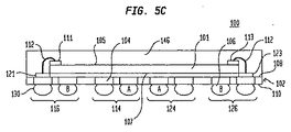
従来の超小型電子パッケージには、メモリ記憶アレイを構成する能動素子を備えた超小型電子素子を組み込むことができる。したがって、いくつかの従来の超小型電子素子では、別の素子の有無にかかわらず、トランジスタ又は他の能動素子がメモリ記憶アレイを構成する。場合によっては、この超小型電子素子は、主としてメモリ記憶アレイ機能を提供するものとして構成することができ、すなわちこの場合、超小型電子素子は、メモリ記憶アレイ機能を提供する能動素子を、他のいかなる機能よりも数多く具体化することができる。場合によっては、超小型電子素子は、DRAMチップ、又はそのような半導体チップを重ねて電気的に相互に接続したアセンブリとすることもできるし、それらを含むものとすることもできる。通常、そのようなパッケージの端子の全ては、超小型電子素子が設けられるパッケージ基板の1以上の周縁部に隣接して列の組(sets of columns)として設けられる。例えば、図1に示している1つの従来の超小型電子パッケージ12において、パッケージ基板20の第1の周縁部16に隣接して端子の3つの列14を設けることができ、パッケージ基板20の第2の周縁部22に隣接して端子の別の3つの列18を設けることができる。従来のパッケージにおけるパッケージ基板20の中央領域24には、端子の列は全くない。図1は更に、パッケージ内の、面28上に素子コンタクト26を有する半導体チップ11を示している。素子コンタクト26は、パッケージ基板20の中央領域24における開口部、例えばボンドウインドウを通じて延びるワイヤボンド30により、パッケージ12の端子の列14、18と電気的に相互に接続されている。場合によっては、超小型電子素子11の面28と基板20との間に接着層32を設け、ワイヤボンドが接着層32の開口部を通って延在する状態で、超小型電子素子と基板との機械的な接続を補強することができる。
Conventional microelectronic packages can incorporate microelectronic elements with active elements that make up a memory storage array. Thus, in some conventional microelectronic elements, transistors or other active elements comprise a memory storage array with or without other elements. In some cases, the microelectronic element can be configured primarily as providing a memory storage array function, i.e., in this case, the microelectronic element replaces an active element that provides the memory storage array function with other elements. It can be embodied more than any function. In some cases, the microelectronic element can be a DRAM chip or an assembly in which such semiconductor chips are stacked and electrically connected to each other, or can include them. Typically, all of the terminals of such a package are provided as a set of columns adjacent to one or more peripheral edges of the package substrate on which the microelectronic elements are provided. For example, in one conventional
上記に鑑みて、超小型電子パッケージにおける端子の配置の改善を行って、特に、そのようなパッケージと、そのようなパッケージを搭載し互いに電気的に相互接続することのできる回路パネルとを備えたアセンブリにおける電気的性能を向上させることができる。 In view of the above, the arrangement of the terminals in the microelectronic package has been improved, in particular with such a package and a circuit panel on which such a package can be mounted and electrically interconnected. The electrical performance in the assembly can be improved.
本発明の一態様によれば、メモリ記憶アレイを構成する複数の能動素子を備えることのできる超小型電子構造体が提供される。この超小型電子構造体は、前記記憶アレイ内の位置を指定するアドレス情報を受信する複数のアドレス入力部を備えている。前記構造体は、第1の表面と、前記第1の表面において露出した端子とを有することができる。前記端子は第1の端子を含むことができる。前記構造体は、前記第1の端子において受信したアドレス情報を前記アドレス入力部に与えるように構成することができる。第1の端子の各々には、前記アドレス入力部のうちの1以上に送られる情報を含む信号の割当てがなされている。前記第1の端子は、前記第1の表面に垂直な仮想平面(theoretical plane)の対向する第1の側及び第2の側に設けられている。前記第1の側に設けられている第1の端子の信号の割当てと、前記第2の側に設けられている第1の端子の信号の割当てとは、前記仮想平面に関して対称である。 According to one aspect of the present invention, a microelectronic structure is provided that can include a plurality of active elements that comprise a memory storage array. The microelectronic structure includes a plurality of address input units that receive address information specifying a position in the storage array. The structure may have a first surface and a terminal exposed on the first surface. The terminal may include a first terminal. The structure may be configured to give address information received at the first terminal to the address input unit. Each of the first terminals is assigned a signal including information to be sent to one or more of the address input units. The first terminals are provided on opposite first and second sides of a virtual plane perpendicular to the first surface. The assignment of the signal of the first terminal provided on the first side and the assignment of the signal of the first terminal provided on the second side are symmetric with respect to the virtual plane.
このような超小型電子構造体の一例として、前記第1の側にある第1の端子の各々信号の割当てと、前記第2の側にある第1の端子の各々の信号割当てとは、鏡像関係にある。 As an example of such a microelectronic structure, each signal assignment of the first terminal on the first side and each signal assignment of the first terminal on the second side are mirror images. There is a relationship.
このような超小型電子構造体の別の例として、前記第1の端子の第1の組及び第2の組の各々は、前記メモリ記憶アレイ内の位置を指定するために十分なアドレス情報を運ぶように構成される。この例において、前記超小型電子構造体は、前記第1の表面において露出した複数の無接続端子(no-connect terminal)を更に備えたものとすることができる。前記第1の側にある第1の端子の各々の位置と、前記第2の側にある無接続端子の位置とは、前記仮想平面に関して対称とすることができる。このような場合、前記第2の側にある第1の端子の各々の位置と、前記第1の側にある無接続端子の位置とは、前記仮想平面に関して対称とすることができる。 As another example of such a microelectronic structure, each of the first and second sets of first terminals has sufficient address information to specify a location in the memory storage array. Configured to carry. In this example, the microelectronic structure may further include a plurality of no-connect terminals exposed on the first surface. The position of each of the first terminals on the first side and the position of the connectionless terminal on the second side can be symmetric with respect to the virtual plane. In such a case, the position of each of the first terminals on the second side and the position of the connectionless terminal on the first side can be symmetric with respect to the virtual plane.
1つ又は複数の例によれば、前記第1の側及び前記第2の側のそれぞれにある第1の端子は、前記記憶アレイ内の単一の記憶位置を一意に指定するために必要な前記アドレス情報を受信するものとして構成することができる。 According to one or more examples, a first terminal on each of the first side and the second side is required to uniquely specify a single storage location in the storage array. The address information can be received.
1つ又は複数の例によれば、前記第1の側及び前記第2の側のそれぞれにある第1の端子は、前記記憶アレイ内の単一の記憶位置を一意に指定するために必要な前記アドレス情報の大部分を受信するものとして構成することができる。 According to one or more examples, a first terminal on each of the first side and the second side is required to uniquely specify a single storage location in the storage array. It can be configured to receive most of the address information.
1つ又は複数の例によれば、前記端子は、前記超小型電子構造体を回路パネルの対応するコンタクトへと電気的に接続するものとして構成することができる。 According to one or more examples, the terminals can be configured to electrically connect the microelectronic structure to corresponding contacts of a circuit panel.
1つ又は複数の例によれば、前記端子は、前記超小型電子構造体を回路パネルの対応するコンタクトへと、ボンドメタルにより電気的に接続するように構成することができる。 According to one or more examples, the terminal can be configured to electrically connect the microelectronic structure to a corresponding contact of the circuit panel by bond metal.
1つ又は複数の例によれば、前記記憶アレイ内の能動素子の数を、前記構造体の他の構成要素内の能動素子の数よりも多くすることができる。 According to one or more examples, the number of active elements in the storage array can be greater than the number of active elements in other components of the structure.
1つ又は複数の例によれば、前記超小型電子構造体は、前記記憶アレイに関する1以上の動作パラメータを不揮発性記憶するシリアルプレゼンス検出(serial presence detect, SPD)素子を更に備えたものとすることができる。 According to one or more examples, the microelectronic structure further comprises a serial presence detect (SPD) element that nonvolatilely stores one or more operating parameters associated with the storage array. be able to.
1つ又は複数の例によれば、前記構造体は、前記記憶アレイのシリアル番号と、欠陥のある位置とのいずれか又は両方を不揮発性記憶するシリアルプレゼンス検出(SPD)素子を更に備えたものとすることができる。 According to one or more examples, the structure further comprises a serial presence detection (SPD) element that nonvolatilely stores either or both of a serial number of the storage array and a defective location. It can be.
1つ又は複数の例によれば、前記超小型電子構造体の第1の表面は、第1の方向を向いている。前記構造体は1以上の半導体チップを有している。前記アドレス入力部は、前記1以上の半導体チップのうちの少なくとも1つの半導体チップの表面において露出している。前記構造体は、前記第1の方向を向いている第1の表面と、前記第1の方向とは反対の方向を向いている第2の表面とを有する基板を更に備えている。前記1以上の半導体チップは、前記基板の第1の表面又は第2の表面のうちの少なくとも一方の上に重なるように設けられている。 According to one or more examples, the first surface of the microelectronic structure is oriented in a first direction. The structure has one or more semiconductor chips. The address input unit is exposed on a surface of at least one of the one or more semiconductor chips. The structure further includes a substrate having a first surface facing the first direction and a second surface facing a direction opposite to the first direction. The one or more semiconductor chips are provided so as to overlap at least one of the first surface and the second surface of the substrate.
1つ又は複数の例によれば、前記超小型電子構造体の第1の表面は、第1の方向を向いている。前記構造体は、前記第1の方向を向いている第1の表面と、前記第1の方向とは反対の方向を向いている第2の表面とを有する基板を備えている。前記1以上の半導体チップのうちの少なくとも1つは、前記基板の第1の表面に重なるように設けられている。 According to one or more examples, the first surface of the microelectronic structure is oriented in a first direction. The structure includes a substrate having a first surface facing the first direction and a second surface facing a direction opposite to the first direction. At least one of the one or more semiconductor chips is provided so as to overlap the first surface of the substrate.
1つ又は複数の例によれば、前記仮想平面は、第1の方向に延びる線において前記第1の表面と交わる第1の仮想平面である。前記端子のうちの少なくともいくつかは、第2の仮想平面の対向する第1の側及び第2の側に設けられている。この第2の仮想平面は、前記第1の表面に垂直であり、かつ、前記第1の方向と交わる第2の方向に沿った第2の線において前記第1の表面と交わっている。前記第2の仮想平面の第1の側に設けられている少なくともいくつかの端子の信号の割当てと、前記第2の仮想平面の第2の側に設けられている少なくともいくつかの端子の信号割当てとは、鏡像関係にある。 According to one or more examples, the virtual plane is a first virtual plane that intersects the first surface in a line extending in a first direction. At least some of the terminals are provided on opposite first and second sides of the second imaginary plane. The second virtual plane intersects the first surface at a second line along a second direction that is perpendicular to the first surface and intersects the first direction. Assignment of signals of at least some terminals provided on the first side of the second virtual plane and signals of at least some terminals provided on the second side of the second virtual plane Allocation has a mirror image relationship.
1つ又は複数の例によれば、前記超小型電子構造体は、複数の第2の能動素子を有するバッファ素子を備えたものとすることができる。前記バッファ素子は、少なくともいくつかのアドレス入力部に送るために、前記アドレス情報を再生することと、部分的に復号化することと、完全に復号化することとのうちの少なくとも1つを行うように構成することができる。 According to one or more examples, the microelectronic structure may comprise a buffer element having a plurality of second active elements. The buffer element performs at least one of reproducing, partially decoding, and fully decoding the address information for sending to at least some address inputs. It can be constituted as follows.
1つ又は複数の例によれば、前記記憶アレイは、互いに少なくとも部分的に重なり合っている、垂直に重ねられた複数の半導体チップのうちの1以上に組み込むことができる。 According to one or more examples, the storage array can be incorporated into one or more of a plurality of vertically stacked semiconductor chips that are at least partially overlapping each other.
1つ又は複数の例によれば、前記超小型電子構造体は、第1の表面を有する基板を備えたものとすることができる。前記基板の第1の表面及び前記超小型電子構造体の第1の表面は第1の方向を向いている。垂直に重ねられた複数の半導体チップは、前記第1の方向とは反対の第2の方向を向いている前記基板の第2の表面に重なっている。 According to one or more examples, the microelectronic structure may comprise a substrate having a first surface. The first surface of the substrate and the first surface of the microelectronic structure are oriented in a first direction. The plurality of vertically stacked semiconductor chips overlaps the second surface of the substrate that faces the second direction opposite to the first direction.
1つ又は複数の例によれば、前記超小型電子構造体は第1の半導体チップ及び第2の半導体チップを備えている。各半導体チップは、前記第1の表面に平行な単一の面内に位置する面を有している。前記アドレス入力部のうちの少なくともいくつかは、前記第1の半導体チップの面において露出したものとすることができ、前記アドレス入力部のうちの少なくともいくつかは、前記第2の半導体チップの面において露出したものとすることができる。 According to one or more examples, the microelectronic structure comprises a first semiconductor chip and a second semiconductor chip. Each semiconductor chip has a surface located in a single plane parallel to the first surface. At least some of the address input units may be exposed on a surface of the first semiconductor chip, and at least some of the address input units may be a surface of the second semiconductor chip. It can be exposed at.
1つ又は複数の例によれば、前記超小型電子構造体は、1以上の半導体チップと、該1以上の半導体チップのうちの少なくとも1つの半導体チップの面に重なる表面を有する誘電体層とを備えている。前記誘電体層の表面は、前記1以上の半導体チップの面から離れる方向を向いている。前記構造体は、誘電体層に沿って延びているトレースと、該トレースから延びており、前記少なくとも1つの半導体チップの表面において露出したアドレス入力部に電気的に接続される金属化ビア(metallized via)とを備えている。前記構造体は、前記端子により受信したアドレス情報を、前記トレース及び前記金属化ビアを通じて前記アドレス入力部へと伝えるように構成することができる。 According to one or more examples, the microelectronic structure includes one or more semiconductor chips and a dielectric layer having a surface that overlaps a surface of at least one of the one or more semiconductor chips. It has. The surface of the dielectric layer faces away from the surface of the one or more semiconductor chips. The structure includes a trace extending along a dielectric layer and a metallized via extending from the trace and electrically connected to an exposed address input at a surface of the at least one semiconductor chip. via). The structure may be configured to transmit address information received by the terminal to the address input unit through the trace and the metallized via.
1つ又は複数の例によれば、前記超小型電子構造体の前記メモリ記憶アレイは、第1のメモリ記憶アレイ及び第2のメモリ記憶アレイを含むことができる。前記超小型電子構造体は、前記第1の側にある前記第1の端子により受信したアドレス情報を前記第1のメモリ記憶アレイに提供するとともに、前記第2の側にある前記第1の端子により受信したアドレス情報を前記第2のメモリ記憶アレイに提供して、デュアルランクメモリアクセスを提供するものとして構成することができる。 According to one or more examples, the memory storage array of the microelectronic structure can include a first memory storage array and a second memory storage array. The microelectronic structure provides address information received by the first terminal on the first side to the first memory storage array and the first terminal on the second side Can be configured to provide address information received by the second memory storage array to provide dual rank memory access.
1つ又は複数の例によれば、前記超小型電子構造体は、シングルランクメモリアクセスを提供するものとして構成することができる。 According to one or more examples, the microelectronic structure can be configured to provide single rank memory access.
本発明の別の態様によれば、超小型電子アセンブリが提供される。この超小型電子アセンブリは、対向する第1の表面及び第2の表面と、それぞれ前記第1の表面及び前記第2の表面にある第1のパネルコンタクト及び第2のパネルコンタクトとを有する回路パネルを備えたものとすることができる。 According to another aspect of the invention, a microelectronic assembly is provided. The microelectronic assembly includes a circuit panel having opposing first and second surfaces, and first and second panel contacts on the first and second surfaces, respectively. Can be provided.
第1の超小型電子構造体及び第2の超小型電子構造体は、前記第1のパネルコンタクト及び前記第2のパネルコンタクトにそれぞれ取り付けられる端子を有している。このような態様によれば、各超小型電子構造体は、メモリ記憶アレイを構成する能動素子と、前記記憶アレイ内の位置を指定するアドレス情報を受信するアドレス入力部とを備えたものとすることができる。前記構造体は、第1の表面と、前記第1の表面において露出した端子とを有することができる。前記端子は第1の端子を含み、前記構造体は、前記第1の端子において受信したアドレス情報を前記アドレス入力部に送るように構成することができる。一例において、各第1の端子には、前記アドレス入力部のうちの1以上に送られる情報を含む信号の割当てをすることができる。前記第1の端子は、前記第1の表面に垂直な仮想平面の対向する第1の側及び第2の側に設けられている。前記第1の側に設けられた第1の端子の信号割当てと、前記第2の側に設けられた第1の端子の信号割当てとは、鏡像関係にある。 The first microelectronic structure and the second microelectronic structure have terminals respectively attached to the first panel contact and the second panel contact. According to such an aspect, each microelectronic structure includes an active element that forms a memory storage array, and an address input unit that receives address information designating a position in the storage array. be able to. The structure may have a first surface and a terminal exposed on the first surface. The terminal may include a first terminal, and the structure may be configured to send address information received at the first terminal to the address input unit. In one example, each first terminal can be assigned a signal containing information sent to one or more of the address inputs. The first terminal is provided on a first side and a second side facing each other on a virtual plane perpendicular to the first surface. The signal assignment of the first terminal provided on the first side and the signal assignment of the first terminal provided on the second side are in a mirror image relationship.
1つ又は複数の例によれば、各超小型電子構造体は1以上の半導体チップを含むことができ、各超小型電子構造体のメモリ記憶アレイは、前記1以上の半導体チップのうちの少なくとも1つに組み込むことができる。各超小型電子構造体の第1の端子は、それぞれの前記超小型電子構造体の少なくとも1つの半導体チップの動作モードを制御する情報を伝える端子を含むことができる。 According to one or more examples, each microelectronic structure can include one or more semiconductor chips, and the memory storage array of each microelectronic structure includes at least one of the one or more semiconductor chips. Can be integrated into one. The first terminal of each microelectronic structure may include a terminal for transmitting information for controlling an operation mode of at least one semiconductor chip of the microelectronic structure.
1つ又は複数の例によれば、前記仮想平面の第1の側及び第2の側のそれぞれにある第1の端子は、それぞれの超小型電子構造体に送られる全てのコマンド信号を運ぶものとして構成することができる。一例では、前記コマンド信号は、書込みイネーブル信号と、行アドレス・ストローブ信号と、列アドレス・ストローブ信号とを含むことができる。 According to one or more examples, the first terminals on each of the first side and the second side of the virtual plane carry all command signals sent to the respective microelectronic structures. Can be configured. In one example, the command signal may include a write enable signal, a row address strobe signal, and a column address strobe signal.
1つ又は複数の例によれば、前記仮想平面の第1の側及び第2の側のそれぞれにある第1の端子は、それぞれの超小型電子構造体に送られるクロック信号を運ぶように構成することができる。前記クロック信号は、前記アドレス情報を運ぶ信号をサンプリングするために用いられるクロックを含む。 According to one or more examples, a first terminal on each of the first side and the second side of the virtual plane is configured to carry a clock signal that is sent to a respective microelectronic structure. can do. The clock signal includes a clock used to sample the signal carrying the address information.
1つ又は複数の例によれば、各超小型電子構造体において、前記仮想平面の第1の側及び第2の側のそれぞれにある第1の端子は、当該超小型電子構造体に送られる全てのバンクアドレス信号(bank address signal)を運ぶように構成することができる。 According to one or more examples, in each microelectronic structure, a first terminal on each of the first side and the second side of the virtual plane is routed to the microelectronic structure. It can be configured to carry all bank address signals.
1つ又は複数の例によれば、前記第1の超小型電子構造体の仮想平面の第1の側にある第1の端子は、前記回路パネルを通じて、前記第2の超小型電子構造体の仮想平面の第2の側にある第1の端子に接続することができる。前記第1の超小型電子構造体の前記第2の側にある第1の端子は、前記回路パネルの前記第1の表面及び第2の表面に平行な、互いに直交するx方向及びy方向に沿った、前記第2の超小型電子構造体の第1の側にある、当該第1の端子が接続される対応する第1の端子の1ボールピッチ以内に位置合わせすることができる。 According to one or more examples, the first terminal on the first side of the imaginary plane of the first microelectronic structure is connected to the second microelectronic structure through the circuit panel. A first terminal on the second side of the virtual plane can be connected. The first terminals on the second side of the first microelectronic structure are parallel to the first surface and the second surface of the circuit panel and in the x and y directions perpendicular to each other. Along the first side of the second microelectronic structure can be aligned within one ball pitch of the corresponding first terminal to which the first terminal is connected.
1つ又は複数の例によれば、前記第1の超小型電子構造体の前記第2の側にある第1の端子は、前記回路パネルの第1の表面及び第2の表面に平行な、互いに直交するx方向及びy方向に沿った、当該端子が接続される前記第2の超小型電子構造体の前記第1の側にある第1の端子と合致させることができる。 According to one or more examples, the first terminals on the second side of the first microelectronic structure are parallel to the first surface and the second surface of the circuit panel, It can be matched with the first terminal on the first side of the second microelectronic structure to which the terminal is connected along the x and y directions orthogonal to each other.
1つ又は複数の例によれば、前記第1の超小型電子構造体の第1の端子のうちの1つと、前記第2の超小型電子構造体の第1の端子のうちの対応する1つとの間の電気的接続のうちの少なくとも1つの電気的接続のスタブの長さは、前記超小型電子構造体の各々の第1の端子の最小ピッチの7倍未満とすることができる。 According to one or more examples, one of the first terminals of the first microelectronic structure and the corresponding one of the first terminals of the second microelectronic structure. The length of the stub of at least one of the electrical connections between the two may be less than 7 times the minimum pitch of each first terminal of the microelectronic structure.
1つ又は複数の例によれば、前記第1の超小型電子構造体の第1の端子と前記第2の超小型電子構造体の第1の端子との間の、前記回路パネルを通じた電気的接続の少なくともいくつかは、前記回路パネルの厚みにほぼ等しい電気的長さとすることができる。 According to one or more examples, electricity through the circuit panel between a first terminal of the first microelectronic structure and a first terminal of the second microelectronic structure. At least some of the electrical connections can be of electrical length approximately equal to the thickness of the circuit panel.
1つ又は複数の例によれば、前記回路パネルの第1の表面及び第2の表面において露出した、電気的に接続される一対の第1のパネルコンタクト及び第2のパネルコンタクトを接続する導電性素子を合わせた全長は、前記パネルコンタクトの最小ピッチの7倍未満とすることができる。 According to one or more examples, the conductive connecting the pair of electrically connected first and second panel contacts exposed at the first and second surfaces of the circuit panel. The total length of the integrated elements can be less than 7 times the minimum pitch of the panel contacts.
1つ又は複数の例によれば、前記回路パネルは、前記超小型電子構造体のそれぞれに送られる全ての前記アドレス情報を運ぶ複数の導体を有するバスを備えることができる。前記導体は、前記回路パネルの第1の表面及び第2の表面に平行な第1の方向に延びたものとすることができる。 According to one or more examples, the circuit panel may comprise a bus having a plurality of conductors carrying all the address information sent to each of the microelectronic structures. The conductor may extend in a first direction parallel to the first surface and the second surface of the circuit panel.
1つ又は複数の例によれば、前記第1の端子は、前記仮想平面の第1の側及び第2の側のそれぞれにある個々の列内に設けることができる。前記回路パネルは、前記第1の超小型電子構造体及び前記第2の超小型電子構造体の第1の端子が電気的に接続される回路パネル上の接続位置と、少なくとも第3の超小型電子構造体の端子が電気的に接続される回路パネル上の別の接続位置との間で全てのアドレス情報をグローバルルーティングするルーティング層を1つのみ備えたものとすることができる。 According to one or more examples, the first terminals can be provided in individual columns on each of the first side and the second side of the virtual plane. The circuit panel includes a connection position on the circuit panel to which the first terminals of the first microelectronic structure and the second microelectronic structure are electrically connected, and at least a third microminiature. It is possible to provide only one routing layer for globally routing all address information to another connection position on the circuit panel to which the terminals of the electronic structure are electrically connected.
1つ又は複数の例によれば、前記仮想平面の第1の側及び第2の側のそれぞれにある第1の端子は、2つの平行な列内の位置に設けることができる。前記回路パネルは、前記超小型電子構造体の1以上の超小型電子構造体の端子が電気的に接続される前記回路パネル上の各接続位置間で全てのアドレス情報をグローバルルーティングするルーティング層を2つのみ備えたものとすることができる。 According to one or more examples, the first terminals on each of the first side and the second side of the virtual plane can be provided at positions in two parallel rows. The circuit panel includes a routing layer that globally routes all address information between connection positions on the circuit panel to which terminals of one or more microelectronic structures of the microelectronic structure are electrically connected. Only two may be provided.
1つ又は複数の例によれば、前記第1の超小型電子構造体及び前記第2の超小型電子構造体の第1の端子が電気的に接続される前記回路パネル上の接続位置と、少なくとも第3の超小型電子構造体の端子が電気的に接続される前記回路パネル上の別の接続位置との間で全ての前記アドレス情報をグローバルルーティングするルーティング層が1つのみ設けることができる。 According to one or more examples, a connection position on the circuit panel to which the first terminals of the first microelectronic structure and the second microelectronic structure are electrically connected; There can be provided only one routing layer for globally routing all the address information with another connection position on the circuit panel to which the terminals of at least the third microelectronic structure are electrically connected. .
図1に関して説明した例示的な従来の超小型電子パッケージ12に鑑みて、本発明者らは、メモリ記憶アレイチップを組み込んだ超小型電子構造体及びそのような超小型電子構造体を組み込んだアセンブリの電気的性能の向上に役立ちうる可能な改善を認識している。
In view of the exemplary conventional
特に、パッケージ等の超小型電子構造体の使用に際して、例えば図2〜図4に示しているようなアセンブリに設けられた場合に、改善をすることができる。これらの図において、パッケージ12Aが回路パネルの表面に設けられ、それと対向するように、別の同様のパッケージ12Bが回路パネルの反対側の表面に設けられている。パッケージ12A、12Bは通常、機能的及び機械的に互いに同等である。機能的及び機械的に同等なパッケージの他の対である12C及び12Dと、12E及び12Fとをも、通常同じ回路パネル34に設けることができる。回路パネルとそれに取り付けられたパッケージとは、一般にデュアルインラインメモリモジュール(dual in-line memory module)(「DIMM」)と呼ばれるアセンブリの一部を構成することができる。対向して設けられたパッケージの各対におけるパッケージ、例えばパッケージ12A、12Bは、回路パネルの対向する表面にあるコンタクトに接続し、各対におけるパッケージ同士が通常、各々の面積の90%以上にわたり互いに重なるものとなっている。回路パネル34内のローカル配線は、端子、例えば各パッケージの「1」、「5」とラベル付けされた端子を回路パネル上のグローバル配線へと接続する。グローバル配線は、接続位置I、II、及びIII等の、回路パネル34上の接続位置に何らかの信号を伝えるためのバス36の信号導体を有する。例えば、パッケージ12A、12Bは、接続位置Iに接続されたローカル配線によってバス36に電気的に接続され、パッケージ12C、12Dは、接続位置IIに接続されたローカル配線によってバスに電気的に接続され、パッケージ12E、12Fは、接続位置IIIに接続されたローカル配線によってバスに電気的に接続されている。
In particular, when a microelectronic structure such as a package is used, it can be improved if it is provided in an assembly such as that shown in FIGS. In these drawings, a
回路パネル34は、十字型すなわち「シューレース」パターンに似たローカル相互接続配線により、パッケージ12A、12Bの各々の端子を電気的に相互接続する。ここで、パッケージ12Aの一方の縁部16付近の「1」というラベルが付された端子は、回路パネル34を通ってパッケージ12Bの同じ側の縁部16付近の、パッケージ12Bの「1」というラベルが付された端子に接続している。しかし、回路パネル34に取り付けられたパッケージ12Bの縁部16は、パッケージ12Aの縁部16から遠くに位置している。図2〜図4はさらに、パッケージ12Aの縁部22付近の「5」というラベルが付された端子が、回路パネル34を通ってパッケージ12Bの同じ縁部22付近の、パッケージ12Bの「5」というラベルが付された端子に接続することも示す。アセンブリ38において、パッケージ12Aの縁部22はパッケージ12Bの縁部22から遠くに位置している。
The
各パッケージ、例えばパッケージ12A上の端子と、その反対側に設けられたパッケージすなわちパッケージ12B上の対応する端子との間の、回路パネルを通る接続は、かなり長いものである。図3から更にわかるように、同様の超小型電子パッケージ12A、12Bのこのようなアセンブリにおいて、回路パネル34は、バス36の信号導体を、バスから同じ信号が各パッケージに送られることになっている場合には、「1」という印がついたパッケージ12Aの端子と、「1」という印がついたパッケージ12Bの対応する端子とに対して、電気的に相互に接続することができる。同様に、回路パネル34は、バス36の別の信号導体を、「2」という印がついたパッケージ12Aの端子と、「2」という印がついたパッケージ12Bの対応する端子とに対して、電気的に相互に接続することができる。同じことが、「3」という印がついた各パッケージ12A、12Bの端子の回路パネル34を通る電気的接続についてもいえる。同じ接続の仕組みを、バスの別の信号導体及びそれぞれのパッケージの対応する端子にも当てはめることができる。回路パネル34上のバス36と、パッケージの各々の対における各パッケージ、例えば、パッケージ12A、12B(図2)との間の、基板の接続位置Iにおけるローカル配線は、非終端型のスタブ(unterminated stub)の形式とすることができる。このようなローカル配線は、比較的長い場合には、場合によっては後述するようにアセンブリ38の性能に影響を及ぼす可能性がある。さらに、回路パネル34においては、他のパッケージ、すなわちパッケージの対12C及び12D並びにパッケージの対12E及び12Fにおけるある端子をバス36のグローバル配線に電気的に相互に接続するようなローカル配線も要求され、このような配線も、同じようにアセンブリの性能に影響を及ぼす可能性がある。
The connection through the circuit panel between each package, for example the terminal on the
図4は更に、信号「1」、「2」、「3」、「4」、「5」、「6」、「7」、及び「8」を伝えるために割り当てられた端子のそれぞれの対における、超小型電子パッケージ12Aと12Bとの間の相互接続を示している。図4からわかるように、端子の列14、18は各パッケージ12A、12Bそれぞれの縁部16、22の付近にあるため、端子の列14、18が延びている方向42に直交する方向40において回路パネル34を横断するために必要な配線は、非常に長くなる可能性がある。DRAMチップ等の超小型電子素子の長さは、それぞれの辺において10ミリメートルの範囲にすることができるということを認識すれば、対向して設けられる2つのパッケージ12A、12Bの対応する端子に同じ信号をルーティングするのに必要な、図2〜図4に示したアセンブリ38における回路パネル34内のローカル配線の長さは、場合によっては5ミリメートルから10ミリメートルの範囲に及ぶ可能性があり、通常は約7ミリメートルとすることができる。
FIG. 4 further illustrates each pair of terminals assigned to carry signals “1”, “2”, “3”, “4”, “5”, “6”, “7”, and “8”. Figure 2 illustrates the interconnection between the
場合によっては、このように対向して設けられる超小型電子パッケージの端子を接続するために必要な回路パネルの配線の長さは、アセンブリの電気的性能にひどく影響を及ぼさない場合がある。しかし、パッケージ12A、12B上の互いに接続された端子の対によって運ばれる信号が、アドレス情報か、又は回路パネルに接続された複数のパッケージのメモリ記憶アレイ機能の動作に共通のアドレス情報をサンプリングするために利用できるクロック情報等の他の情報かを伝えるために用いるバス36からの信号である場合には、バス36からそれぞれのパッケージ上の端子まで延びているスタブの配線長さが性能に著しく影響を及ぼす場合があるということを本発明者らは認識している。相互接続を行う配線が比較的長い場合には、より甚だしく影響があり、それによって、送信信号の整定時間、リンギング、ジッタ、又は符号間干渉が受け入れがたい程度にまで増大する可能性がある。
In some cases, the length of the circuit panel wiring required to connect the terminals of the microelectronic package provided in this manner may not significantly affect the electrical performance of the assembly. However, the signal carried by the pair of mutually connected terminals on the
特定の実施形態において、アドレス情報を伝えるために用いるバス36は、コマンド情報、アドレス情報、バンクアドレス情報、及びクロック情報を伝えるためのコマンド・アドレス・バス36とすることができる。具体的な実施にあたり、コマンド情報は、回路パネル上のそれぞれの信号導体上のコマンド信号として送信することができる。アドレス情報を、それぞれの信号導体上のアドレス信号として送信することもでき、バンクアドレス情報を、それぞれの信号導体上のバンクアドレス信号として送信することもでき、クロック情報を、それぞれの信号導体上のクロック信号として送信することもできる。DRAMチップ等のメモリ記憶アレイを有する超小型電子素子の具体的な実施にあたり、バス36が運ぶことができるコマンド信号は、書込み許可(write enable)、行アドレス・ストローブ、及び列アドレス・ストローブとすることができ、バス36が運ぶことができるクロック信号は、少なくともバス36が運ぶアドレス信号をサンプリングするためのクロック信号とすることができる。
In certain embodiments, the
したがって、本明細書において説明する本発明のある実施形態によれば、このような第1のパッケージ及び第2のパッケージが、回路パネル、例えば回路基板、モジュール基板若しくはカード、又はフレキシブル回路パネルの、向かい合った面に対向するように設けられる場合に、回路パネル上のスタブの長さを短くできるように構成された超小型電子パッケージが提供される。互いに向かい合うように回路パネルに設けられた第1の超小型電子パッケージ及び第2の超小型電子パッケージを組み込んだアセンブリは、それぞれのパッケージ間のスタブの長さを非常に短くすることができる。このようなアセンブリにおいてスタブの長さを短くすると、例えばなかでも整定時間、リンギング、ジッタ、又は符号間干渉のうちの1以上を低減することにより、電気的性能を向上させることができる。さらに、回路パネルの構造の単純化、又は回路パネルの設計若しくは製造、若しくは回路パネルの設計及び製造の両方の複雑性及びコストの低減等、他の利点もまた得ることができる。 Thus, according to certain embodiments of the invention described herein, such first package and second package are circuit panels such as circuit boards, module boards or cards, or flexible circuit panels. Provided is a microelectronic package configured to reduce the length of a stub on a circuit panel when provided to face opposite surfaces. An assembly incorporating the first microelectronic package and the second microelectronic package provided on the circuit panel so as to face each other can greatly reduce the length of the stub between the respective packages. Shortening the stub length in such an assembly can improve electrical performance, for example, by reducing one or more of settling time, ringing, jitter, or intersymbol interference. In addition, other advantages can also be obtained, such as simplification of the structure of the circuit panel, or reduction in complexity and cost of circuit panel design or manufacture, or both circuit panel design and manufacture.
先に述べたような、本発明の実施形態による超小型電子構造体100を図5及び図5Aに示している。図5に示しているように、構造体100は、第1の表面201と、複数の端子、例えば第1の表面において露出した第1の端子104及び第2の端子106とを有している。本明細書において、導電性素子が構造体の表面「において露出する(exposed at)」という表現は、上記導電性素子が、上記構造体の外側からその表面に向かってその表面に対して垂直な方向に移動する仮想点(theoretical point)との接触のために利用できることを意味する。したがって、構造体の表面において露出する端子又は他の導電性素子は、そのような表面から突出したものとすることができるか、そのような表面と同一平面をなすものとすることができるか、又はそのような表面から後退し、その構造体内の穴又はくぼみを通じて露出したものとすることができる。
A
超小型電子構造体100は、その上に能動素子202、例えば、トランジスタのような能動デバイス、若しくは他の能動素子を含むことができ、これらの能動素子により、他の素子の有無にかかわらず、メモリ記憶アレイ204が構成される。一例では、能動素子202、及び能動素子によって構成されるメモリ記憶アレイ204は、超小型電子構造体の1つの超小型電子素子の一部内に、又は1以上の超小型電子素子、例えば、1以上の半導体チップ内に組み込むことができるか、又は超小型電子構造体の1以上の超小型電子パッケージ又はそのアセンブリ内に組み込むことができる。限定はされないが、一例では、超小型電子構造体100は、例えば、超小型電子パッケージ若しくはその一部とすることができ、パッケージの第1の表面において端子が露出する。別の例では、超小型電子構造体は、電気的に接続された複数の超小型電子パッケージを含むアセンブリとすることができるか、又は電気的に接続された超小型電子素子、半導体チップ、又は超小型電子素子若しくは半導体チップの一部、又は超小型電子パッケージの一部を含む構造とすることができる。
The
一例では、メモリ記憶アレイ204は、超小型電子構造体の機能部を含み、その機能部は、超小型電子構造体の別の機能部の補助的な役割を果たすことができる。例えば、超小型電子構造体は、論理機能部、例えばプロセッサと、メモリ機能部とを含むことができ、メモリ機能部は、論理機能部の機能を支援することができるか、又は論理機能部の機能を果たすことを助けることができる。しかし、特定の例では、超小型電子構造体は、主にメモリ記憶アレイ機能を提供するように構成することができる。後者の場合、超小型電子構造体は、メモリ記憶アレイ機能を提供する能動素子202、例えばトランジスタなどの能動デバイスを、その構造体のメモリ記憶アレイ機能以外の機能を提供する他の構成要素における能動素子よりも、数多く有することができる。
In one example, the
超小型電子構造体は、メモリ記憶アレイ204内の位置を指定するアドレス情報を受信するための複数のアドレス入力部206を有することができる。したがって、アドレス入力部は、上記のように超小型電子素子の表面において露出するコンタクトとすることができる。超小型電子構造体は、その超小型電子構造体の特定の端子が受信したアドレス情報をアドレス入力部206へと送るように構成されている。例えば、超小型電子構造体は、構造体の特定の端子において受信された信号を、対応する特定のアドレス入力部206へとつなぐことができる。特定の例では、アドレス入力部は、超小型電子素子101、例えば、半導体チップの面207において露出したものとすることができる。面207は、超小型電子構造体の第1の表面201と向かい合っている。別の例では、アドレス入力部206は、第1の表面201から離れた側にある、超小型電子素子101の面209において露出したものとすることができる。一例では、超小型電子構造体は、その中に配線を含むことができ、配線は、一組の端子、例えば、「第1の端子」104を、構造体の対応するアドレス入力部と電気的に直接的に接続することができる。本明細書において、「第1の端子」104の各々は、1以上のアドレス入力部206を含む超小型電子構造体における信号割当てを有する。別の例では、後に更に説明するように、超小型電子構造体は、その上に複数の能動素子を有する半導体チップ等のバッファ素子を含むことができ、このような半導体チップは、超小型電子構造体によってアドレス入力部に送るために第1の端子が受信したアドレス又はコマンド情報のうちの少なくとも1つを再生することと、部分的に復号化することと、完全に復号化することとのうちの少なくとも1つを行うように構成される。コマンド情報は、超小型電子構造体内のメモリ記憶アレイ又はその一部の動作モードを制御する情報とすることができる。
The microelectronic structure can have a plurality of
超小型電子構造体は、超小型電子構造体の「シリアルプレゼンス検出(serial presence detect, SPD)素子」として「SPD」機能を実行する少なくとも一部分を有する不揮発性メモリを更に備えたものとすることができる。そのようなSPD素子は、超小型電子構造体の編成、タイミング又は容量のうちの少なくとも1つに関連する動作パラメータを含むことができる。一実施形態では、SPD素子は、メモリ記憶アレイが設けられ、かつアドレス入力部によってアドレス情報が提供される1以上の半導体チップ以外の半導体チップ内に組み込むことができる。一例では、動作パラメータは、使用可能状態において超小型電子構造体の回路によって行アドレス・ストローブ(row address strobe)信号が検出された後の待ち時間のクロックサイクル数のようなタイミング(これ以降、「RAS待ち時間」とする)に関連する場合があるか、又は使用可能状態において超小型電子構造体の回路によって列アドレス・ストローブ信号が検出された後の待ち時間のクロックサイクル数に関連する場合があるか、又は例えば、1ギガバイト(「1Gb」)、2ギガバイト(「2Gb」)等の超小型電子構造体の容量に関連する場合があるか、又は「シングルランク」、「2ランク」、「4ランク」若しくは他の構造体等の超小型電子構造体の編成に関連する場合があるか、又は他の動作パラメータ、若しくは上記の動作パラメータの組み合わせ、若しくは他の動作パラメータに関連する場合がある。一例では、不揮発性メモリは、限定はされないが、上記のパラメータのうちの1つのパラメータの情報を記憶することができるか、又は動作パラメータの任意の組み合わせの情報を記憶することができる。特定の例では、SPDは、メモリ記憶アレイへの読出し又は書込みアクセス中に回避されるべきである、超小型電子構造体のメモリ記憶アレイ内の既知の不良メモリ位置のテーブルを含むことができる。 The microelectronic structure may further comprise a non-volatile memory having at least a portion that performs the “SPD” function as a “serial presence detect (SPD) element” of the microelectronic structure. it can. Such SPD elements can include operational parameters related to at least one of organization, timing, or capacity of the microelectronic structure. In one embodiment, the SPD element can be incorporated in a semiconductor chip other than one or more semiconductor chips that are provided with a memory storage array and whose address information is provided by an address input unit. In one example, the operating parameter may be a timing such as the number of clock cycles of latency after the row address strobe signal is detected by the microelectronic structure circuitry in the enabled state (hereinafter “ RAS latency "), or may be related to the number of clock cycles of latency after the column address strobe signal is detected by the microelectronic structure circuitry in the available state. Or may be related to the capacity of a microelectronic structure such as 1 gigabyte (“1 Gb”), 2 gigabyte (“2 Gb”), or “single rank”, “2 rank”, “ May be related to the organization of microelectronic structures such as “4 ranks” or other structures, or other operating parameters, or Combination of parameters, or may be associated with other operating parameters. In one example, the non-volatile memory can store information of one of the above parameters, but is not limited to, or can store information of any combination of operating parameters. In a particular example, the SPD may include a table of known bad memory locations within the microelectronic structure memory storage array that should be avoided during read or write access to the memory storage array.
仮想平面(theoretical plane)132は、超小型電子構造体の対向する第1の縁部140と第2の縁部141との間の位置において、第1の表面201に対して垂直な方向に沿って超小型電子構造体を通って延びている。仮想平面と他の構造体との間の関係は、後に述べる例から明らかになるであろう。図5Aから更にわかるように、超小型電子構造体100は、仮想平面132の対向する第1の側及び第2の側に設けられた複数の第1の端子、例えば、複数の端子104を有している。これらの端子は、第1の表面において露出している導電性素子、例えば、コンタクト、パッド、ポスト、ピン、ソケット、配線とすることができる。場合によっては、これらの端子は、導電性結合材料等を用いて、別の素子、例えば、回路パネルの対応するコンタクトに導通可能に接続されるように構成することができ、場合によっては、結合材料は、なかでも、ハンダ、スズ又は金のようなボンドメタルとすることができる。このような場合に、それらの端子は、端子、例えばパッド又はポストの金属製素子の表面に取り付けられる、ハンダボール、金バンプ、金属及びポリマ材料を含む導電性マトリックス材料、又は上記の材料のうちの1以上の組み合わせ等の、可融導電性材料の接合素子を含むことができる。他の場合には、それらの端子は、各構成要素の対応する導電性素子間の圧入又は締り嵌め等によって、別の構成要素の対応する機構に対し機械的にかつ電気的に係合するように構成することができ、場合によっては、それらの端子が係合する対応する導電性表面に対してスライド又はワイプすることもできる。
A
図5A及び図5Bから更にわかるように、第1の端子104のうちの第1の組が仮想平面132の第1の側に設けられ、第1の端子104のうちの同じ構成の第2の組が、第1の側と向かい合う仮想平面132の第2の側に設けられている。超小型電子構造体は、第1の端子により受信されたアドレス情報をアドレス入力部に与えるように構成されている。本明細書において、超小型電子素子若しくはその一部のアドレス情報、又はコマンド・アドレス・バス情報、又は信号及びアドレス入力の文脈において用いられる場合に、「端子上のアドレス情報がアドレス入力部に与えられる」という表現は、端子上のアドレス情報が、アドレス入力との電気的接続を介して、又は端子により受信されたアドレス情報の再生、部分的な復号化又は復号化のうちの少なくとも1つを実行することができるバッファ素子を通して、アドレス入力部に送られることを意味する。図5Aから更にわかるように、第1の端子104のうちの第1の組の信号割当ては、第1の端子104のうちの第2の組の信号割当ての鏡像となっている。
As can be further understood from FIGS. 5A and 5B, the first set of the
本明細書において、仮想平面132の両側にそれぞれ設けられた第1の端子の対の信号割当ては、その対の各端子に割り当てられる信号が機能的に同等である場合に、互いに鏡像の関係にある。アドレス空間内の位置を指定する際に別の信号と同じ機能を有するあるアドレス信号は、その別のアドレス信号と機能的に同等である。このことは、超小型電子構造体上の一対のアドレス端子、例えば、「A2L」(A2_Left)及び「A2R」(A2_Right)がそれぞれ、同じアドレス空間内のある位置を指定するために用いられるアドレス内の重み22(2の2乗)のビットを指定するという例において、最も明らかである。各信号A2L及びA2Rを用いて、同じアドレス空間内、又は同等のアドレス空間内のアドレスの同様の部分を指定することができるため、これらの端子は同じ信号割当てを有する。それによる一例では、パッケージA2L及びA2Rの端子の一方又は両方のいずれかに送られるアドレス情報は、超小型電子構造体100(図5)内に組み込まれた1以上の超小型電子素子において同じ名称「A2」を有する対応するアドレス入力部、例えば、素子コンタクトに送ることができることは明らかである。したがって、一例では、鏡像信号割当てを有する第1の端子の各対に割り当てられる信号、例えば、第1の端子のうちの第1の組内の信号A2L及び第2の組内の信号A2Rは、超小型電子構造体の外部の場所にあるドライバ回路の同一の出力から生じるものとすることができる。さらに、そのような例では、信号A2L及びA2Rが超小型電子構造体の端子により受信される、回路パネルの外部に露出したパネルコンタクトは別々であるが、場合によっては、それらのパネルコンタクトは、回路パネルの1以上の他の場所において電気的に互いに結び付けることができる。したがって、場合によっては、一対の同等の信号A2L及びA2Rは、そのような他の回路パネルの場所において単一の信号として運ばれる。
In the present specification, the signal assignments of the first terminal pairs provided on both sides of the
別の例では、超小型電子構造体は複数の超小型電子素子を備えることができ、それらの超小型電子構造体においては、超小型電子構造体内の超小型電子素子のうちの1以上に対し、同じ構造体の超小型電子素子のうちの別の1以上に与えられるアドレス情報とは別にアドレス情報が与えられる。この場合、仮想平面の第1の側及び第2の側のそれぞれにある端子の第1の組及び第2の組によりアドレス信号が受信されるが、仮想平面の第1の側にある第1の端子により受信されるアドレス情報は、超小型電子構造体の1以上の第1の超小型電子素子のアドレス入力部にのみ与えることができる。逆に、第1の側とは反対側の、仮想平面の第2の側にある第1の端子により受信されるアドレス情報は、超小型電子構造体の超小型電子素子のうちの1以上の第2の超小型電子素子のアドレス入力部にのみ与えることができる。一例では、1以上の第1の超小型電子素子は、仮想平面の第1の側に設けることができ、1以上の第2の超小型電子素子は、仮想平面の第2の側に設けることができる。このような場合、信号割当てとしてA2Lを有する、パッケージの端子により受信されるアドレス情報と、それと鏡像関係にある信号割当てA2Rを有する、パッケージの端子により受信されるアドレス情報とはそれぞれ、超小型電子構造体100(図5)のそれぞれの第1の超小型電子素子及び第2の超小型電子素子の同じ名称「A2」を有する素子コンタクトに送ることができる。 In another example, the microelectronic structure can comprise a plurality of microelectronic elements, in which the microelectronic structure includes one or more of the microelectronic elements in the microelectronic structure. Address information is given separately from address information given to one or more other microelectronic elements having the same structure. In this case, the address signal is received by the first set and the second set of terminals on the first side and the second side of the virtual plane, respectively, but the first signal on the first side of the virtual plane. The address information received by the terminals can be provided only to the address input of one or more first microelectronic elements of the microelectronic structure. Conversely, address information received by the first terminal on the second side of the virtual plane opposite the first side is one or more of the microelectronic elements of the microelectronic structure. It can be given only to the address input section of the second microelectronic element. In one example, the one or more first microelectronic elements can be provided on the first side of the virtual plane, and the one or more second microelectronic elements can be provided on the second side of the virtual plane. Can do. In such a case, the address information received by the terminal of the package having A2L as the signal assignment and the address information received by the terminal of the package having the signal assignment A2R that is in a mirror image relationship with each other are the microelectronics. Each of the first microelectronic element and the second microelectronic element of structure 100 (FIG. 5) can be sent to an element contact having the same name “A2”.
それぞれの第1のグリッド114及び第2のグリッド124に設けることのできる、第1の端子のうちの第1の組及び第2の組の各組の信号割当ては、仮想平面132に関して対称であるものとして示している。信号A15を受信するものとして割り当てられた第1の組の端子114−1と、信号A15を受信するものとして割り当てられた第2の組の対応する端子124−1とは、仮想平面132に関して対称である。仮想平面132の対向する第1の端子どうしの同じ関係が、図5において、及び本願の他の図において与えられる種々の断面図に表されている。具体的には、このような図における表記「A」は、アドレス入力部に送られることになるアドレス情報を受信するために同じ信号割当てを有する一対の第1の端子の場所を表しており、このような第1の端子は、各超小型電子構造体100等においてそれぞれ鏡像関係にある位置に設けられる。
The signal assignments of each of the first set and the second set of the first terminals that can be provided in the respective
場合によっては、仮想平面の第1の側及び第2の側のそれぞれにある第1の端子は、記憶アレイ内の単一の記憶場所を一意的に指定するために必要な各信号を受信するように構成することができる。他の場合には、第1の側及び第2の側のそれぞれにある第1の端子は、記憶アレイ内の単一の記憶場所を一意的に指定するために必要な信号の大部分のみを受信するように構成することができる。 In some cases, a first terminal on each of the first side and the second side of the virtual plane receives each signal necessary to uniquely specify a single storage location in the storage array. It can be constituted as follows. In other cases, the first terminal on each of the first side and the second side may only provide a majority of the signals required to uniquely specify a single storage location in the storage array. It can be configured to receive.
仮想平面132は、縁部141よりも縁部140の近くに存在するものとすることができるか、又は縁部140よりも縁部141の近くに存在するものとすることができる複数の位置において超小型電子構造体を通って延びているものとすることができるが、特定の例において、かつ図5Aに示しているように、仮想平面は縁部140と141との間の中間的な位置において構造体100を通って延びるものとすることができる。
The
図5Aにおいて更に示しているような特定の例では、超小型電子構造体の第1の表面201は第1の方向214に面しており、超小型電子構造体100は、同じ第1の方向に面した第1の表面110を有する基板102を有している。基板102の第2の表面108は、第1の方向とは反対の第2の方向216に面したものとすることができる。
In a specific example, as further shown in FIG. 5A, the
そのような例では、場合によっては、能動素子202のうちのいくつか又は全てが設けられる半導体チップ等の超小型電子素子101は、基板102の第2の表面108から離れた側の面209を有することができる。図5Cにおける特定の例において更にわかるように、超小型電子構造体100内に組み込まれる超小型電子素子101は、その前面105に素子コンタクト111、113を有することができ、それらのコンタクトは、基板102の第2の表面108にあるそれぞれの基板コンタクト121、123に電気的に接続される。例えば、ワイヤボンド112により素子コンタクト111、113と基板コンタクト121、123とを電気的に接続することができる。あるいは、他のタイプの導体、例えば、リードフレームの一部、可撓性リボンボンド等を用いて、素子コンタクト111、113を、それぞれの基板コンタクト121、123と電気的に接続することができ、場合によっては、素子コンタクト111、113を、超小型電子素子101の前面105よりも、基板表面108から高い位置に設けられる他の導電性素子と接続することができる。1つのタイプのこのような超小型電子素子101では、素子コンタクト111、113のうちのいくつかのコンタクトはそれぞれ、超小型電子素子に供給されるアドレス情報のうちの特定のアドレス情報を受信できるように構成することができる。特定の実施形態では、そのようなコンタクト111、113はそれぞれ、超小型電子素子の外部から、すなわち、ワイヤボンド112等のパッケージの配線を通って、かつ第1の端子104を通って、超小型電子素子101に供給されるアドレス信号を受信するアドレス入力部とすることができる。また、コンタクト111、113は、限定はされないが、ワイヤボンド112及び第2の端子106等を通して、超小型電子素子の外部から他の情報又は信号を受信するように構成することもできる。
In such an example, in some cases, the
こうした超小型電子素子101の特定の一例において、それぞれの超小型電子素子が用いるクロックのエッジに対して、すなわち、異なる第1の電圧状態と第2の電圧状態との間でのクロックの遷移において、素子コンタクト111、113において存在するアドレス信号をサンプリングすることができる。すなわち、それぞれのアドレス信号は、クロックのより低電圧の状態とより高電圧の状態との間の上昇の遷移において、又は、クロックのより高電圧の状態とより低電圧の状態との間の下降の遷移においてサンプリングすることができる。したがって、複数のアドレス信号はクロックの上昇の遷移において全てサンプリングすることもできるし、そのようなアドレス信号はクロックの下降の遷移において全てサンプリングすることもできるし、又は、別の例において、素子コンタクト111、113のうちの1つにおけるアドレス信号は、クロックの上昇の遷移においてサンプリングすることができ、別の1つの外部のコンタクトにおけるアドレス信号は、クロックの下降の遷移においてサンプリングすることができる。
In one particular example of such a
主としてメモリ記憶アレイ機能を提供するように構成することのできる別のタイプの超小型電子素子101において、アドレスコンタクトのうちの1以上を多重方式で用いることができる。この例において、それぞれの超小型電子素子101の特定の素子コンタクト111、113は、外部から超小型電子素子に供給される互いに異なる2つ以上の信号を受け取ることができる。したがって、第1のアドレス信号は異なる第1の電圧状態と第2の電圧状態との間のクロックの第1の遷移(例えば、上昇の遷移)において、特定のコンタクト111、113においてサンプリングすることができ、第1のアドレス信号以外の信号は、第1の電圧状態と第2の電圧状態との間のクロックの、第1の遷移とは反対の第2の遷移(例えば、下降の遷移)において、特定のコンタクトにおいてサンプリングすることができる。
In another type of
このような多重方式において、それぞれの超小型電子素子101の同じ素子コンタクト111、113上で、クロックの同じサイクル内で2つの異なった信号を受け取ることができる。特定の場合において、この方法での多重化により、それぞれの超小型電子素子101の同じ素子コンタクト111、113において、同じクロックサイクル内で第1のアドレス信号と、それとは別の信号とを受け取ることができる。更に別の例において、この方法での多重化によって、第1のアドレス信号と、別の第2のアドレス信号とを、それぞれの超小型電子素子101の同じ素子コンタクト111、113において同じクロックサイクル内で受け取ることができる。
In such a multiplexing scheme, two different signals can be received within the same cycle of the clock on the
いくつかの実施の形態において、基板102は、シート状又はボード状の誘電体素子を含むことができ、誘電体素子は、本質的に、ポリマ材料、例えば、なかでも樹脂又はポリイミドからなることができる。あるいは、基板は、例えばBT樹脂又はFR−4構成のガラス繊維強化エポキシ等の複合的構成を有する誘電体素子を含むことができる。いくつかの例では、誘電体素子は、誘電体素子の平面内で、すなわち、基板102の第1の表面110に平行な方向に、最大30パーツパーミリオン/摂氏温度(以下、「ppm/℃」)の熱膨張率を有する。別の例では、基板は、端子及び他の導電性構造体が配置される、12パーツパーミリオン/摂氏温度未満の熱膨張率(coefficient of thermal expansion)(「CTE」)を有する材料の支持要素を含むことができる。例えば、こうしたCTEが小さい素子は、本質的に、ガラス材料、セラミック材料、半導体材料、若しくは液晶ポリマ材料、又はこうした材料の組合せからなることができる。
In some embodiments, the
図5Cからわかるように、基板コンタクトの第1の組121及び第2の組123が、基板の第2の表面108において露出したものとすることができる。基板コンタクトの第1の組121は、例えば、超小型電子素子の面105の上方に延びる導電性構造体を通して、超小型電子素子の素子コンタクト132の列111(図6A)と電気的に接続することができる。この導電性構造体は例えば、ワイヤボンド112とすることができる。場合によっては、超小型電子素子の背面107と基板102の第2の表面108との間にダイのアタッチ用の接着剤を設けることができ、超小型電子素子と基板との間の接続を機械的に強化することができる。基板コンタクトの第2の組123は、素子コンタクト131の列113(図6A)と電気的に接続することができる。
As can be seen from FIG. 5C, the
図6Aから更にわかるように、超小型電子素子130の縁部170が第1の方向142に沿って延びたものとすることができ、縁部170に隣接するコンタクト131の列111が面105に沿って同じ第1の方向142に延びたものとすることができる。縁部170に対して平行な、超小型電子素子130の別の縁部172が第1の方向142に延び、コンタクト131の第2の列113が、縁部172に隣接して面105に沿って同じ第1の方向142に延びたものとすることができる。図6Aに更に示しているように、超小型電子素子上のコンタクトの列は、列111の場合のように完全に設けることができるか、又は列113の場合のように、列内の場所のうちのいくつかにおいてのみコンタクトを設けることができる。ワイヤボンド112(図5C)等の導電性構造体により、コンタクト111、113を、基板の第2の表面108において露出する対応するコンタクト121、123と電気的に接続することができる。
As can be further seen in FIG. 6A, the
図6Bは、図6Aに示した実施形態の変形形態を示している。超小型電子素子180のコンタクト131を、超小型電子素子180のそれぞれの周縁部170、172、176、178に隣接する列及び行内に配置し、それらの周縁部と位置合わせすることできる。縁部170、172は平行であり、第1の方向142に延びている。
FIG. 6B shows a variation of the embodiment shown in FIG. 6A. The
図6Cは、図6Aに示した実施形態の別の変形形態を示している。超小型電子素子190のコンタクトは、超小型電子素子の縁部170、172に隣接する列188及び189内に配置される。しかし、この場合、超小型電子素子190は、導電性再分配層を有する半導体チップを有し、コンタクト131は、再分配コンタクトの列188、189を含むことができ、それらのコンタクトは半導体チップのコンタクト192、194と接触するように形成された導電性トレース又は金属化ビア(metallized via)によって、半導体チップのコンタクト192、194に接続される(又は金属化ビア及びトレースの両方によってチップのコンタクト192、194に接続することができる)。この場合、コンタクト192、194は、場合によっては、半導体のバックエンドオブライン(back end of line)(「BEOL」)配線を通して半導体チップの能動素子と接続することができ、その配線は、ビア又は他の導電性構造体を含むことができ、場合によってはコンタクト192、194の下に配置することもできる。
FIG. 6C shows another variation of the embodiment shown in FIG. 6A. The contacts of the
図6A〜図6Cに特に示しているように、いくつかの実施形態では、超小型電子素子のコンタクトは、コンタクト192の列のように単一列で配置することができるか、又は、コンタクト111、113の列について示すように複数の列で配置することができる。各列は、方向142に沿う列の各垂直レイアウト位置にコンタクトを含むことができるか、又は、コンタクトは、コンタクト113の列の1つの列の場合と同様に列の1以上の位置から欠落させることができる。特定の実施形態では、コンタクトは、図6Aに示したようなコンタクトの配置に代えて、超小型電子素子の面105(図5C)上のエリアアレイ内に、すなわち、図6Aに示す超小型電子素子の面105、若しくは面105の或る部分の上に分布するエリアアレイ等のエリアアレイ内に配置することができる。別の例では、超小型電子素子のコンタクトは、図5Bで超小型電子素子の境界をマーク付けした破線で示す超小型電子素子の1以上の周辺縁部に隣接してコンタクトの1以上の組で配置することができる。特定の例では、超小型電子素子は単一半導体チップとすることができ、超小型電子素子上のコンタクト111又は113は、半導体チップのコンタクトである「チップコンタクト」とすることができる。
As shown particularly in FIGS. 6A-6C, in some embodiments, the contacts of the microelectronic element can be arranged in a single row, such as a row of
別の例では、図6Cを参照すると、特定の超小型電子素子190が、面105において露出するチップコンタクト192の単一の列を有することができる。チップコンタクト192の単一の列は、超小型電子素子の対向する第1の縁部170及び第2の縁部172に対して平行に、かつその中間にある仮想軸174に、又はその近くに配置することができ、軸174に対して平行な方向に延びたものとすることができる。例えば、面105は、超小型電子素子190の第1の縁部170及び第2の縁部172にそれぞれ隣接する第1の周辺領域及び第2の周辺領域を有することができ、チップコンタクト192の列は、第1の周辺領域184と第2の周辺領域186との間に見られる面105の中央領域181に配置することができる。中央領域は、第1の縁部170及び第2の縁部172に対して平行な仮想の境界182及び183によって定められるエリア内に配置することができる。本明細書において、超小型電子素子又は半導体チップの面の「中央領域」は、その面の対向する第1の縁部及び第2の縁部に対して平行な方向において、その面の寸法全体を通して延びている平行な境界を有する、その面のエリアを意味し、中央領域は、対向する第1の縁部と第2の縁部との間の面の最短寸法の中央の3分の1に及ぶ。したがって、第1の周辺領域は、中央領域と第1の縁部との間の面の最短寸法の3分の1に及び、第2の周辺領域は、中央領域と第2の縁部との間の最短寸法の3分の1に及ぶ。
In another example, referring to FIG. 6C, a particular
一例では、ワイヤボンド112は、チップコンタクト192のそのような列から、コンタクト121等の基板コンタクト、又はコンタクト123まで直接延在することができる。代替的には、いくつかのワイヤボンド112がそのようなチップコンタクト192からコンタクト121まで延在することができ、いくつかのワイヤボンド112がそのようなチップコンタクト192からコンタクト123まで延在することができる。
In one example, the
代替的には、超小型電子素子は2列以上のチップコンタクトを有することができる。例えば、図6Cは、第1のチップコンタクト列192及び第2のチップコンタクト列194を有する超小型電子素子を示す。各チップコンタクト列192、194は、軸174に隣接して、例えば、軸174に極めて近接して、すなわち、中央領域181内に配置することができる。場合によっては、超小型電子素子は、3列以上のコンタクトを有することもできる。
Alternatively, the microelectronic element can have more than one row of chip contacts. For example, FIG. 6C shows a microelectronic element having a first
図6Cに示す特定の例では、超小型電子素子は、チップコンタクトの第1の列192及び第2の列194を有することができ、コンタクト111又は113は、再分配コンタクトを含むことができ、再分配コンタクトは、超小型電子素子の面105上に形成され、また、例えばトレース及びビア等の導電性素子によってチップコンタクトに電気的に接続される。特に断らない限り、本明細書の例のそれぞれにおける超小型電子素子の「コンタクト」は、述べたこれらの方法の任意の方法で配置することができる。
In the particular example shown in FIG. 6C, the microelectronic element can have a
超小型電子素子は、素子コンタクトの列内に配置されない場合がある別のコンタクトも含むことができる。場合によってはこれらの更なるコンタクトを、電力、接地に接続するために、又は、試験をするために使用することができるようなプロービングデバイスとの接触のために利用可能なコンタクトとして使用することができる。 The microelectronic element can also include other contacts that may not be placed in the array of element contacts. In some cases these additional contacts may be used as contacts available for connection to power, ground, or for contact with a probing device such as can be used for testing. it can.
図5Cに見られるように、パッケージ100は、例えば回路パネル等の、パッケージ100の外部の構成要素にパッケージ100を電気的かつ機械的に接続する第1の端子104及び第2の端子106を有することができる。端子104、106は、導電性パッド、ポスト、又は他の導電性構造体とすることができる。図5Cに示す例では、端子は、場合によっては、なかでもはんだ、錫、インジウム、金、若しくは共晶材料等のボンドメタル又は他の導電性ボンド材料を含むことができるような接合要素130を含むことができ、また場合によっては、導電性パッド又はポスト等の基板の導電性構造体に取り付けられる導電性バンプ等の更なる構造体も含むことができる。第1の端子104及び第2の端子106は、例えばトレース及びビア等の基板上の導電性構造体を通して基板コンタクト121、123に電気的に接続することができる。特定の例では、第1の端子104のうちの第1の組は、第2の表面108と対向する基板102の第1の表面110において露出する第1のグリッド114内の場所に設けることができる。第1の端子104のうちの第2の組は、基板の第1の表面110において露出する第2のグリッド124内の位置に設けることができ、仮想平面132の、第1の端子のうちの第1の組とは反対側に配置されている。図のいくつかでは、第1の組及び第2の組は、超小型電子素子の前面の外側境界を越えて延在するように示しているが、それは、必ずしも当てはまらない。本発明のある特定の実施形態では、各組における第1の端子の組は、上述のアドレス情報、又は特定の実施形態では、上述のアドレス情報及びコマンド・アドレス・バスの或る特定の信号を運ぶように構成することができる。
As seen in FIG. 5C, the
例えば、超小型電子素子101がDRAM半導体チップを含むかDRAM半導体チップである場合、第1の組及び第2の組のそれぞれは、パッケージ内の回路が、例えば、行アドレス及び列アドレスのデコーダ、並びにもしある場合にはバンク選択回路が使用して、パッケージにおける超小型電子素子内のメモリ記憶アレイの全ての利用可能なアドレス指定可能であるメモリ位置からアドレス指定可能なメモリ位置を決定することのできる、超小型電子パッケージ100に送られるアドレス情報を運ぶように構成される。特定の実施形態において、第1の組及び第2の組のそれぞれは、そのようなメモリ記憶アレイ内のアドレス指定可能なメモリ位置を決定するために超小型電子パッケージ100内のそのような回路が用いるアドレス情報の全てを運ぶように構成することができる。
For example, when the
そのような実施形態の変形形態において、第1のグリッド114及び第2のグリッド124内の位置に設けられた第1の端子は、そのようなメモリ記憶アレイ内のアドレス指定可能なメモリ位置を決定するために超小型電子パッケージ100内のそのような回路が用いるアドレス情報の大部分を運ぶように構成することができる。その場合には、超小型電子パッケージ上の上述の第2の端子106のうちの少なくともいくつか等の他の端子が、アドレス情報の残りの部分を運ぶように構成される。そのような変形形態において、特定の実施形態において、第1の組及び第2の組のそれぞれにおける第1の端子は、そのようなメモリ記憶アレイ内のアドレス指定可能メモリ位置を決定するのに超小型電子パッケージ100内のそのような回路が用いるアドレス情報の3/4以上を運ぶように構成される。
In a variation of such an embodiment, a first terminal provided at a location within the
特定の実施形態において、第1の組及び第2の組、例えば、グリッド114、124のそれぞれはチップセレクト情報、例えば、チップ内のメモリ記憶位置にアクセスするために超小型電子パッケージ100内の特定のチップを選択するのに利用できる情報を運ぶように構成されない場合がある。別の実施形態において、第1の組及び第2の組のうちの少なくとも1つにおける第1の端子は、実際にチップセレクト情報を運ぶことができる。
In certain embodiments, each of the first set and the second set, eg,
通常、超小型電子パッケージ100内の超小型電子素子101がDRAMチップであるか、DRAMチップを含む場合には、一実施形態におけるアドレス信号は、パッケージの外部の構成要素、例えば、後述の回路パネル154(図7A)等の回路パネルからパッケージに送られる全てのアドレス情報を含むことができ、それを用いて超小型電子パッケージ内のランダムアクセスアドレス指定可能メモリ位置を決定してそこに読み取りアクセス、又は読み取りアクセス又は書込みアクセスのどちらかを行う。
Usually, when the
第2の端子106のうちの少なくともいくつかは、第1の組及び第2の組を有する第1の端子104によって運ばれるアドレス信号以外の信号を運ぶように構成することができる。特定の例では、第2の端子106は、チップセレクト、リセット、電源電圧、例えば、Vdd、Vddq及び接地、例えば、Vss及びVssq等のデータ、データ・ストローブ信号又は他の信号若しくは基準電位のうちの1以上を運ぶことができる。第2の端子の一部又は全ては、第1の端子のうちの第1の組及び第2の組が配置される、同じ第1のグリッド114及び第2のグリッド124内の位置にも配置することができる。そのような場合に、第1のグリッド114及び第2のグリッド124内の場所に配置されるいくつかの端子を、データ、データ・ストローブ信号、又はチップセレクト、リセット、電源電圧、例えば、Vdd、Vddq及び接地、例えば、Vss及びVssq等の他の信号若しくは基準電位のうちの1以上を運ぶように構成することができる。第3のグリッド116及び第4のグリッド126内の場所に配置されるいくつかの端子を、データ、データ・ストローブ信号、又はチップセレクト、リセット、電源電圧、例えば、Vdd、Vddq及び接地、例えば、Vss及びVssq等の他の信号若しくは基準電位のうちの1以上を運ぶように構成することができる。
At least some of the
特定の実施形態において、各超小型電子パッケージの第1のグリッド114及び第2のグリッド124の第1の端子は、超小型電子素子101の動作モードを制御する情報を運ぶように構成することができる。より具体的には、第1の端子の第1の組及び第2の組のそれぞれは、超小型電子パッケージ100に送られるコマンド信号及びクロック信号の少なくとも一方の特定の一組すべてを運ぶように構成することができる。一実施形態において、第1の組及び第2の組を有するそれぞれの第1の端子104は、外部の部品、例えば回路パネル又は他の素子から超小型電子パッケージ100へと送られるコマンド信号、アドレス信号、バンクアドレス信号、及びクロック信号のすべてを運ぶように構成することができ、このコマンド信号は、行アドレス・ストローブ、列アドレス・ストローブ、及び書込み許可を含む。
In certain embodiments, the first terminals of the
超小型電子素子のうちの1以上がダイナミックランダムアクセスメモリ(「DRAM」)半導体チップ又はDRAMチップのアセンブリによって提供されるもの等のダイナミックメモリ記憶アレイ機能を提供するように構成される一実施形態においては、コマンド信号は、書込み許可、行アドレス・ストローブ、及び列アドレス・ストローブ信号とすることができる。ODT(on die termination)(ダイの上にある終端)、チップセレクト、クロックイネーブル等の他の信号は、グリッド114、124等の第1の組及び第2の組内に置かれている端子が運ぶ場合もあるし、運ばない場合もある。クロック信号は、アドレス信号をサンプリングするのに超小型電子素子のうちの1以上が用いるクロックとすることができる。例えば、図7の超小型電子パッケージにおいて、また、図5Aに更に示すように、 第1の端子104は、アドレス信号A0〜A15(A0及びA15を含む)、及びバンクアドレス信号BA0、BA1及びBA2だけでなく、クロック信号CK及びCKB、行アドレス・ストローブ(row address strobe)RAS、列アドレス・ストローブ(column address strobe)CAS、及び書込み許可(write enable)信号WEも運ぶように構成することができる。
In one embodiment, one or more of the microelectronic elements are configured to provide a dynamic memory storage array function, such as that provided by a dynamic random access memory (“DRAM”) semiconductor chip or an assembly of DRAM chips. The command signal may be a write enable, row address strobe, and column address strobe signal. Other signals such as on-die termination (ODT), chip select, clock enable, etc. are connected to terminals located in the first and second sets of
超小型電子素子のうちの1以上がダイナミックランダムアクセスメモリ(「DRAM」)半導体チップ又はDRAMチップのアセンブリによって提供されるもの等のダイナミックメモリ記憶アレイ機能を提供するように構成される一実施形態においては、コマンド信号は、書込み許可、行アドレス・ストローブ、及び列アドレス・ストローブ信号とすることができる。ODT(ダイの上にある終端)、チップセレクト、クロックイネーブル等の他の信号は、グリッド114、124等の第1の組及び第2の組内に配置されている端子が運ぶ場合もあるし、運ばない場合もある。クロック信号は、アドレス信号をサンプリングするのに超小型電子素子のうちの1以上が用いるクロックとすることができる。例えば、図7Aに示している超小型電子パッケージ100Aにおいて、また、図5Aに更に示すように、 第1の端子104は、アドレス信号A0〜A15(A0及びA15を含む)、及びバンクアドレス信号BA0、BA1及びBA2だけでなく、クロック信号CK及びCKB、行アドレス・ストローブRAS(row address strobe)、列アドレス・ストローブ(column address strobe)CAS、及び書込み許可信号(write enable)WEも運ぶように構成することができる。
In one embodiment, one or more of the microelectronic elements are configured to provide a dynamic memory storage array function, such as that provided by a dynamic random access memory (“DRAM”) semiconductor chip or an assembly of DRAM chips. The command signal may be a write enable, row address strobe, and column address strobe signal. Other signals such as ODT (terminating on the die), chip select, clock enable, etc. may be carried by terminals located in the first and second sets of
一実施形態では、アドレス信号以外の信号を運ぶように構成される第2の端子106の少なくともいくつかは、第1のグリッド114及び第2のグリッド124内の位置に配置することができる。一例では、コマンド信号、アドレス信号、及びクロック信号以外の信号を運ぶように構成される第2の端子106の少なくともいくつかは、第1のグリッド114及び第2のグリッド124内の位置に配置することができる。図面において、第2の端子106の特定の構成を示しているが、図示の特定の構成は例示の目的のためであり、限定することを意図したものではない。例えば、第2の端子106は、電源又は接地信号に接続するように構成される端子も含むことができる。
In one embodiment, at least some of the
パッケージの第1のグリッド114及び第2のグリッド124内の第1の端子の配置構成は、図5A〜図5Cに特に示している。一例では、各グリッド114、124は、端子の、平行な第1の列及び第2の列136を含むことができる。各グリッド内の端子の列136は互いに隣接させることができる。代替的に、図5A〜図5Cには示していないが、少なくとも1つの端子を、端子の第1の列と第2の列との間に配置することができる。図5Bに見られる等の別の例では、グリッドは、列の軸119が、こうした列の端子104の大部分を通って延びる、すなわち、列の端子104の大部分に対して中央に置かれる、端子の列を含むことができる。しかし、こうした列では、端子の1以上は、端子104’の場合と同様に、列の軸119に対して中央に置かれない場合がある。この場合、これらの1以上の端子は、たとえこうした端子(複数可)が軸119に対して中央に置かれなくても、特定の列の一部と考えられる。その理由は、こうした端子が、任意の他の列の軸より、その特定の列の軸119に近いからである。列の軸119は、列の軸に対して中央に置かれていないこれらの1以上の端子を通して延びることができるか、又は場合によっては、中央に置かれない端子は、列の軸119が、列の中央に置かれないこれらの端子を通過する可能性がないように、列の軸からより遠くにあるものとすることができる。1つの列内に、又は更に、グリッド内のそれぞれの列の列軸に対して中央に置かれない2つ以上の列内に、1つの、いくつかの、又は多くの端子が存在する場合がある。
The arrangement of the first terminals in the
パッケージの第1のグリッド114及び第2のグリッド124内の第1の端子の配置構成は、図5A〜図5Cに特に示している。一例では、図5Bに示しているように、各グリッド114、124は、端子の平行な第1の列及び第2の列136を含むことができる。各グリッド内の端子の列136は互いに隣接させることができる。あるいは、図5A〜図5Cに示していないが、少なくとも1つの端子を、端子の第1の列と第2の列との間に配置することができる。図5Bに見られる等の別の例では、グリッドは、列軸119が、こうした列の端子104の大部分を通って延在する、すなわち、列の端子104の大部分に対して中央に置かれる、端子の列を含むことができる。しかし、こうした列では、端子の1以上は、端子104’の場合と同様に、列軸119に対して中央に置かれない場合がある。この場合、これらの1以上の端子は、たとえこうした端子(複数可)が軸119に対して中央に置かれなくても、特定の列の一部と考えられる。その理由は、こうした端子が、任意の他の列の軸より、その特定の列の軸119に近いからである。列軸119は、列軸に対して中央に置かれないこれらの1つ又は複数の端子を通して延在することができるか、又は場合によっては、中央に置かれない端子は、列軸119が、列の中央に置かれないこれらの端子を通過する可能性がないように、列軸からより遠くにあることができる。1つの列内に、又は更に、グリッド内のそれぞれの列の列軸に対して中央に置かれない2つ以上の列内に、1つの、いくつかの、又は多くの端子が存在する場合がある。
The arrangement of the first terminals in the
図5において提供される上記の例におけるように、また、図5Aにも示されるように、第2のグリッド124内の第1の端子の信号割当ては、第1のグリッド114内の第1の端子の信号割当て124と鏡像の関係にある。換言すれば、第1のグリッド及び第2のグリッド内の第1の端子の信号割当ては、第1のグリッド114と第2のグリッド124との間の仮想平面又は仮想軸132に関して対称である。軸132は、この場合、第1の端子の列136が延びる方向142に延びている。第2のグリッド124内の信号割当てが第1のグリッド114内の信号割当ての鏡像である状態において、信号A15を運ぶように割当てられる第1のグリッド114の第1の端子114−1は、信号A15を運ぶように割当てられる第2のグリッド124の対応する第1の端子124−1とグリッド内で同じく相対的に垂直方向の位置に(方向142に沿って)ある。しかし、第1のグリッド114が2つの列136を含み、信号A15を運ぶように割当てられる第1のグリッド114の端子114−1が、第1のグリッド114の2つの列136の中の左列内にあるため、鏡像配置構成により、信号A15を運ぶように割当てられる第2のグリッド124の対応する端子124−1が、第2のグリッド124の2つの列の中の右列内にあることが要求される。この配列のもうひとつの結果は、信号A9を運ぶように割り当てられた端子もまた、第1のグリッド114及び第2のグリッド124のそれぞれにおいて同じ、グリッド内での相対的に垂直方向の場所にあるということである。しかし、第1のグリッド114において、A9を運ぶように割り当てられた端子114−1は、第1のグリッド114の2つの列136のうちの右側の列にあり、配列が鏡像であるためには、信号A9を運ぶように割り当てられた第2のグリッド124の対応する端子124−2は、第2のグリッド124の2つの列のうちの左側の列になければならない。図5Aからわかるように、第1のグリッド及び第2のグリッドのそれぞれにおけるそれぞれの第1の端子について、少なくとも、上述の超小型電子構造体のアドレス入力を受信するアドレス情報を運ぶように割り当てられたそれぞれの第1の端子について、同じ関係が当てはまる。
As in the above example provided in FIG. 5 and also shown in FIG. 5A, the signal assignment of the first terminal in the
第1の端子の信号割当ての対称性の基準となる仮想平面132は、基板上の種々の場所に位置させることができる。仮想平面132は、いくつかの実施形態ではパッケージの中心軸であることができる軸とみなすことができ、その中心軸は、特に、第1の端子の列136が縁部140、141に平行な方向に延在し、第1のグリッド及び第2のグリッドが、この中心軸の回りで対称である位置に配置されるとき、基板の対向する第1の縁部140及び第2の縁部141から等距離に位置付けられる。一例では、軸132は、基板の第1の縁部140及び第2の縁部141に対して平行で、かつ等距離にあるラインから任意の2つの隣接する端子列間の最小ピッチの3.5倍以下の距離内に位置させることができる。代替的に、この対称軸132は、縁部140と141との間で等距離である中心軸から水平方向135にオフセットさせることができる。
The
特定の例では、第1のグリッド及び第2のグリッド内の端子は、パッケージの中央領域内に設けることができる。一例では、第1のグリッド114及び第2のグリッド124のそれぞれにおける端子の少なくとも1つの列136は、基板の第1の縁部140及び第2の縁部141から等距離にあり、かつ平行であるラインから任意の2つの隣接する平行な端子列136間の最小ピッチの3.5倍以下の距離内に設けることができる。
In a particular example, the terminals in the first grid and the second grid can be provided in the central region of the package. In one example, at least one
上記で述べたように、第2の端子106は、上記で述べたアドレス情報以外の情報又はコマンド・アドレス・バスの上記で述べた信号以外の信号を運ぶように構成することができる。一例では、第2の端子106は、超小型電子素子への、及び/又は超小型電子素子からの単方向又は双方向のデータ信号及びデータ・ストローブ信号、並びに、データマスク信号及び終端抵抗に対して並列終端をオン又はオフにするために使用されるODT信号すなわち「ダイ上終端(on die termination)」信号を運ぶために使用される端子を含むことができる。特定の例では、チップセレクト、リセット、クロックイネーブル等の信号、並びに、電源電圧等の基準電位、例えばVdd、Vddq、又は接地、例えばVss及びVssqは、第2の端子106によって運ぶことができる。いくつかの実施形態では、コマンド・アドレス・バス信号以外の信号を運ぶように構成される一部又は全ての端子が、適切に設置することができる場所であればどこへでも、パッケージに第2の端子106として設けることができる。例えば、第2の端子106の一部又は全ては、第1の端子104が設けられる基板102上の同じグリッド114、124内に配置することができる。第2の端子106の一部又は全ては、第1の端子104の一部又は全てと同じ列内に又は異なる列内に配置することができる。場合によっては、1以上の第2の端子は、その同じグリッド又は列内の第1の端子に組み入れることができる。
As described above, the
特定の例では、第2の端子106のうちの一部又は全ては、基板の第1の表面110において露出する第3のエリア又はグリッド116内に設けることができ、第2の端子の別の組は、第1の表面110において露出する第4のエリア又はグリッド126内に設けることができる。特定の場合、第3のエリア又はグリッド116内の第2の端子の信号割当ては、第1のグリッド及び第2のグリッドについて上述した方法と同様の方法で、第4のエリア又はグリッド126内の第2の端子の信号割当ての鏡像とすることができる。第3のグリッド116及び第4のグリッド126は、場合によっては、第1のグリッド及び第2のグリッドが延びる方向134に延在することができ、また、互いに平行とすることができる。第3のグリッド及び第4のグリッドも、第1のグリッド114及び第2のグリッド124に平行とすることができる。代替的には、図5Aを参照すると、第2の端子が配置されるグリッド127、137は、方向142と交わるか、更には直交する別の方向135に沿って延びることができる。別の例では、いくつかの第2の端子は、図5Aに示したグリッド116、126、127及び137のそれぞれの中に配置することができる。いくつかの第2の端子も、第1のグリッド114及び第2のグリッド124内の場所に配置することもしないこともできる。
In a particular example, some or all of the
また、図5Aに示しているように、グリッド127における第2の端子の信号クラス割当ては、垂直軸132に関して対称とすることができ、グリッド137における第2の端子の信号クラス割当ては、垂直軸132に関して対称とすることができる。本明細書において、2つの信号クラス割当ては、それらの信号割当てが同じ割当てのクラスにある場合には、たとえそのクラス内での数値インデックスが異なっていようと、互いに関して対称とすることができる。例示的な信号クラス割当ては、データ信号、データ・ストローブ信号、データ・ストローブ補数信号、及びデータマスク信号を含むことができる。特定の例において、グリッド127において信号割当てDQSH、DQSLを有する第2の端子は、たとえそれらの第2の端子が異なる信号割当てを有していようと、データ・ストローブである自らの信号クラス割当てについて垂直軸132に関して対称である。
Also, as shown in FIG. 5A, the signal class assignment of the second terminal in
図5Aに更に示すように、例えばデータ信号DQ0、DQ1、...等についてのデータ信号の超小型電子パッケージ上の第2の端子の空間的位置への割り当ては、垂直軸132に関してモジュロXの対称性(modulo-X symmetry)を有することができる。このモジュロXの対称性は、1以上の対の第1のパッケージ及び第2のパッケージが互いに対向して回路パネルに設けられ、回路パネルは対向して設けられたそれぞれのパッケージの対における第1のパッケージ及び第2のパッケージの対応する第2の端子の対に電気的に接続する、図7A及び図7B等において見られるアセンブリ200又は354における信号の品質(signal integrity)を保つのに役立ちうる。端子の信号割当てが或る軸に関して「モジュロXの対称性」を有する場合には、同じ番号の「モジュロX」を有する信号を運ぶ端子が、その軸に関して対称である位置に置かれる。したがって、図7A及び図7B等におけるそのようなアセンブリ200又は354において、モジュロXの対称性により回路パネルを介した電気的接続を行うことができ、第1のパッケージの端子DQ0が回路パネルを介して同じモジュロX(この場合Xは8)の数値を有する第2のパッケージの端子DQ8に電気的に接続することができ、回路パネルの厚みを本質的に真っ直ぐ通る、すなわちそれに垂直な方向に接続を行うことができるようになっている。したがって、8モジュロ8の演算の結果の数は0であり、9モジュロ8の演算の結果の数は1である。それゆえ、信号割当てがモジュロ8の対称性を有する場合、モジュロ1演算が「1」の結果をもたらす、DQ1等の信号を運ぶように構成される端子は、モジュロ8演算が同じ結果、すなわち、「1」をもたらす、DQ9又はDQ17等の信号を運ぶように構成される別の端子と、1つの軸に関して対称となる基板上の位置に置かれる。
As further shown in FIG. 5A, for example, the assignment of data signals for data signals DQ0, DQ1,... To the spatial location of the second terminal on the microelectronic package is modulo X with respect to
一例において、「X」は2n(2のn乗)という数字とすることができる。ただしnは2以上である。又は、Xは8×Nとすることができる。ただし、Nは2以上である。したがって一例において、Xは、1/2バイトにおけるビット数(4ビット)、1バイトにおけるビット数(8ビット)、複数バイトにおけるビット数(8×N、ただしNは2以上)、ワードにおけるビット数(32ビット)、又は複数ワードにおけるビット数と等しくすることができる。そのようにして、一例において、図5Aに示したようにモジュロ8の対称性がある場合には、データ信号DQ0を運ぶように構成されたグリッド127におけるパッケージ端子DQ0の信号割当ては、データ信号DQ8を運ぶように構成された別のパッケージ端子DQ8の信号割当てと垂直軸132に関して対称である。さらに、垂直軸の回りのグリッド137137におけるパッケージ端子DQ0及びDQ8の信号割当てについても同じことが当てはまり、グリッド137についても同じことが当てはまる。本明細書において説明するもの等のモジュロ8の対称性は、パッケージ端子DQ0〜DQ15の信号割当てのそれぞれに関してグリッド127、137において見ることができる。
In one example, “X” may be a number 2n (2 to the power of n). However, n is 2 or more. Or, X can be 8 × N. However, N is 2 or more. Therefore, in one example, X is the number of bits in 1/2 byte (4 bits), the number of bits in 1 byte (8 bits), the number of bits in multiple bytes (8 × N, where N is 2 or more), the number of bits in a word (32 bits), or the number of bits in multiple words. Thus, in one example, if there is a modulo-8 symmetry as shown in FIG. 5A, the signal assignment of package terminal DQ0 in
図示はしていないが、モジュロ数「X」は2n(2のn乗)以外の数字とすることができ、2よりも大きな任意の数とすることができることに注意することが重要である。したがって、対称性の基礎であるモジュロ数Xは、パッケージがそのために組み立てられる又は構成されるデータサイズにおいて存在するビット数によって決めることができる。例えば、データサイズが8ビットではなく10ビットである場合には、信号割当てはモジュロ10の対称性を有することができる。データサイズが奇数ビットを有する場合には、モジュロ数Xはそのような数を有することができる場合さえあってもよい。 Although not shown, it is important to note that the modulo number “X” can be any number other than 2n (2 to the power of n) and can be any number greater than 2. Therefore, the modulo number X, which is the basis of symmetry, can be determined by the number of bits present in the data size for which the package is assembled or configured. For example, if the data size is 10 bits instead of 8 bits, the signal assignment can have modulo 10 symmetry. If the data size has odd bits, the modulo number X may even be able to have such a number.
図5Dは、図5を参照して上記で説明した超小型電子構造体100の別の例を示している。図5Dの例では、超小型電子素子101の面207は、上記の例と同じように反対に面する第2の表面108の上に重なるのではなく、基板102の第1の表面110の上に重なることができる。この場合、第1の端子104の第1の組114及び第2の組124は、超小型電子素子101のエリアの外部に位置決めすることができる。図5Dにおいて更に見られるように、超小型電子構造体100の接合素子130を含む第1の端子104は、超小型電子素子101の高さH2を収容し、端子を、回路パネル90の表面95において露出した対応するコンタクト92と位置合わせし、かつ接合できるようにするために十分な高さH1を与えるものである。図5Eの例において示しているように、第1の超小型電子構造体100A及び第2の超小型電子構造体100Bからなる垂直に重ねられたアセンブリを構成できるように、第2の超小型電子構造体100Bが、第1の超小型電子構造体100Aの第2の表面108において露出した端子の対応する組314、316に接合される第1の端子104を有することができる。
FIG. 5D shows another example of the
別の例では、図5Fに示されるように、図5に対して上記で論じられたような編成を有する、超小型電子構造体又はパッケージ220が、図5Dに対して上記で説明されたように超小型電子構造体100の上方に垂直に配置されることが示されている。超小型電子構造体220の端子222は、端子、例えば、超小型電子構造体100の第1の端子104及び第2の端子106に関して図5、図5Aにおいて図示され、上記で説明されたようにすることができる。端子222は、以下のように、超小型電子構造体100の第2の表面108において露出する端子314、316と位置合わせし、接合することができるか、又は別の方法で電気的に相互接続することができる。
In another example, as shown in FIG. 5F, a microelectronic structure or
別の例では、図5Fに示しているように、図5に対して上記で論じられたような編成を有する、超小型電子構造体又はパッケージ220が、図5Dに対して上記で説明されたように超小型電子構造体100の上方に垂直に配置されることが示されている。超小型電子構造体220の端子222は、端子、例えば超小型電子構造体100の第1の端子104及び第2の端子106に関して図5、図5Aにおいて図示され、上記で説明したようにすることができる。端子222は、以下のように、超小型電子構造体100の基板102の第2の表面108において露出する端子314、316と位置合わせし、接合することができるか、又は別の方法で電気的に相互接続することができる。
In another example, as shown in FIG. 5F, a microelectronic structure or
一例では、図5Aにおいて与えられるようなボールアウト(ball-out)、すなわち、端子構成を有する超小型電子構造体は、業界標準規格DDR3又はDDR4仕様に従って動作する超小型電子素子を含む超小型電子構造体のために用いることができる。 In one example, a microelectronic structure having a ball-out or terminal configuration as provided in FIG. 5A includes a microelectronic element that operates according to industry standard DDR3 or DDR4 specifications. Can be used for structures.
図5Hは、図5、図5A及び図5Bに示した本発明の実施形態の変形形態による超小型電子構造体のための端子構成を示している。図5Hの変形形態は、超小型電子構造体240の仮想平面132の第1の側241に配置される第1の端子のうちの第1の組242と、仮想平面の第2の側243に配置される第1の端子のうちの第2の組244との間に対称性を与えることができる別の方法を示している。この例では、上記の例の場合と同様に、第1の端子のうちの第1の組及び第2の組はそれぞれ、メモリ記憶アレイ内の位置を指定するために十分なアドレス情報を運ぶように構成することができる。場合によっては、各組242、244は、メモリ記憶アレイ内の位置を指定するために必要となるアドレス情報の大部分のみを運ぶことができる。
FIG. 5H shows a terminal configuration for a microelectronic structure according to a variation of the embodiment of the present invention shown in FIGS. 5, 5A and 5B. The variant of FIG. 5H has a
図5Hに示したような例では、アドレス情報を超小型電子構造体内の1以上のメモリ記憶アレイのアドレス入力部に送るのに必要とされない場合がある仮想平面の各側にある無接続端子(no-connect terminal)の組を設けることができる。本明細書において、超小型電子構造体の「無接続端子」は、そのような無接続端子上に何らかの情報が存在するか否かにかかわらず、超小型電子構造体内の任意の電気経路、例えば、任意の超小型電子素子、例えば、半導体チップに情報を伝達するための経路に接続されない端子を意味する。したがって、無接続端子に接続される超小型電子構造体外部の別の構成要素から接続される場合があるように、無接続端子に情報が存在する場合があっても、無接続端子に存在する情報は、超小型電子構造体内の任意の超小型電子素子に設けられる経路内には存在しない。 In the example as shown in FIG. 5H, unconnected terminals on each side of the virtual plane that may not be required to send address information to the address inputs of one or more memory storage arrays in the microelectronic structure ( no-connect terminal) pairs can be provided. As used herein, a “non-connecting terminal” of a microelectronic structure refers to any electrical path within the microelectronic structure, for example, whether or not there is any information on such non-connecting terminals, Means a terminal not connected to a path for transmitting information to any microelectronic element, for example, a semiconductor chip. Therefore, even if information may be present in the non-connection terminal, it may be present in the non-connection terminal, as may be connected from another component outside the microelectronic structure connected to the non-connection terminal. Information is not present in the path provided in any microelectronic element within the microelectronic structure.
この場合、第1の側における第1の端子それぞれの場所は、仮想平面132の第2の側にある無接続端子の場所と、仮想平面に関して対称とすることができ、第2の側における第1の端子それぞれの場所は、第1の側にある無接続端子の場所と仮想平面に関して対称である。したがって、図5Hにおいて見られるように、例えば、フィールド0(242)として示される、その面の第1の側241における第1の端子の組のうちの第1の端子それぞれの場所は、フィールド0(NC)として示される、面132の第2の側243に設けられた無接続端子の組のうちの無接続端子の位置と、仮想平面132に関して対称である。また、図5Hにおいて、フィールド1(244)として示される、面132の第2の側243の組のうちの各第1の端子の場所と、フィールド1(NC)として示される、面の第1の側241に設けられた無接続端子の組のうちの無接続端子の場所とは、仮想平面132に関して対称である。
In this case, the location of each of the first terminals on the first side can be symmetric with respect to the location of the connectionless terminal on the second side of the
一方の側にある第1の端子とその反対側にある無接続端子との間の対称性に関する上記の要件が満たされる限り、面の同じ側(例えば、第1の側241)にある第1の端子の組及び無接続端子の組は、任意の適切な場所に配置することができる。面132の一方の側にある第1の端子の組が配置される空間は、連続している必要はない。面132の一方の側にある無接続端子の組が配置される空間も連続している必要はない。したがって、仮想平面の同じ第1の側241上のフィールド0(242)として示した第1の端子の組の場所と、フィールド1(NC)として示した無接続端子の組の場所とは、その構造体の表面の重なり合わないエリアを占有する必要はなく、すなわち、第1の側241の第1の端子の組のうちの第1の端子の場所は、互いに混在することを含む、第1の側241の無接続端子に対して任意の適切な場所に配置することができる。さらに、同じ関係は、面132の第2の側にある第1の端子及び無接続端子にも適用することができる。実際には、一例において、その面の一方の側にある各端子及び各無接続端子は、共通のグリッド内の任意の場所に配置することができる。
As long as the above requirements regarding symmetry between the first terminal on one side and the unconnected terminal on the opposite side are met, the first on the same side of the surface (eg, the first side 241) The set of terminals and the set of non-connected terminals can be arranged at any appropriate location. The space in which the first terminal set on one side of the
一例では、図5Hによる超小型電子構造体の第2の端子の場所は、図5Hに更に見られるようにすることができる。この場合、第2の端子の組246、248、250及び252は、図5、図5A及び図5Bに対して上記で説明されたようにすることができるか、又は本明細書において更に図示及び説明されるようにすることができる。
In one example, the location of the second terminal of the microelectronic structure according to FIG. 5H can be further seen in FIG. 5H. In this case, the second set of
一例では、図5Hにおいて表されるようなボールアウト、すなわち、端子構成を有する超小型電子構造体は、業界標準規格LPDDR3仕様に準拠する超小型電子素子を含む超小型電子構造体に用いることができる。 In one example, a microelectronic structure having a ballout or terminal configuration as represented in FIG. 5H is used for a microelectronic structure that includes microelectronic elements that conform to industry standard LPDDR3 specifications. it can.
図7Aは、回路パネル154の対向する第1の表面150及び第2の表面152に設けられるような、第1の超小型電子パッケージ100A及び第2の超小型電子パッケージ100Bのアセンブリ200を示している。特定の内部構造を有する超小型電子構造体を示してきたが、いくつかの例では、各超小型電子構造体100は、図5、図5A、図5A〜C、図5D、図5E、図5F若しくは図5Gのいずれかを参照して上記で図示及び説明されたようにすることができるか、又は本明細書において別の方法で図示及び説明されるようにすることができる。各超小型電子構造体100Aは、その向かい側に設けられる超小型電子構造体100Bと同じ内部構造を有することができるか、又は超小型電子構造体100Aは、他方の超小型電子構造体100Bとは異なった内部構造とすることができる。回路パネルは、なかでも、デュアルインラインメモリモジュール(「DIMM」)で使用されるプリント回路基板、システム内の他の構成要素と接続される回路基板若しくはパネル、又はマザーボード等の種々のタイプとすることができる。第1の超小型電子構造体100A及び第2の超小型電子構造体100Bは、回路パネル154の第1の表面150及び第2の表面152において露出した対応するコンタクト160、162にそれぞれ取り付けることができる。
FIG. 7A shows an
図7Aに特に示しているように、各パッケージの第2のグリッド内の第1の端子の信号割当てが、各パッケージの第1のグリッド内の第1の端子の信号割当ての鏡像であるため、パッケージ100A、100Bが互いに対向する回路パネルに実装されると、第1のパッケージ100Aの第1のグリッド114A内のそれぞれの第1の端子は、第2のパッケージ100Bの第2のグリッド124B内の同じ信号割当てを有する対応する第1の端子と位置合わせすることができ、その対応する第1の端子に電気的に接続される。さらに、第1のパッケージ100Aの第2のグリッド124A内のそれぞれの第1の端子は、第1のグリッド114B内の同じ信号割当てを有する対応する第1の端子に位置合わせすることができ、その対応する第1の端子に電気的に接続される。
As specifically shown in FIG. 7A, the signal assignment of the first terminal in the second grid of each package is a mirror image of the signal assignment of the first terminal in the first grid of each package, When the
確かに、接続された端子の各対の位置合わせは、ある許容誤差以内とすることができ、それにより、接続された端子の各対は、回路パネル154の第1の表面150に沿って直交するx方向及びy方向に沿って、互いに1ボールピッチ以内で位置合わせすることができる。図7Aから明らかであるように、各グリッドの第1の端子は、回路パネルの表面350に平行な、直交するx方向及びy方向において互いに1ボールピッチ以内で位置合わせすることができる。ボールピッチは、いずれかのパッケージ上の任意の2つの隣接する平行な端子列間の最小ピッチ以下である。特定の例において、グリッドは、第1の超小型電子パッケージ及び第2の超小型電子パッケージ上の第1の端子のうちの少なくともいくつかが互いに合致するよう、x方向及びy方向に沿って互いに位置合わせすることができる。本明細書において、回路パネルの互いに向かい合う表面のパッケージの第1の端子が互いに「合致する」場合、位置合わせは慣例的な製造公差内とすることができ、又は第1の回路パネル及び第2の回路パネルの表面に平行な直交するx方向及びy方向に沿って互いに1ボールピッチの半分よりも小さい公差内とすることができる。ボールピッチは上述のとおりである。
Indeed, the alignment of each pair of connected terminals can be within some tolerance, so that each pair of connected terminals is orthogonal along the
特定の例では、それぞれの第1のパッケージ100A及び第2のパッケージ100Bの位置合わせされたグリッド(例えば、第1のパッケージの第1のグリッド114A及び第2のパッケージの第2のグリッド124B)の場所の少なくとも半分は、回路パネル154の第1の表面150に沿って直交するz方向及びy方向において互いに位置合わせすることができる。
In a specific example, each of the aligned grids of the
そのため、図7Aに更に示しているように、第1のパッケージ100Aのグリッド114A内で「A」と記号が付いた信号を運ぶ特定の第1の端子は、同じ信号「A」を運ぶ第2のパッケージ100Bのグリッド124Bの対応する第1の端子に位置合わせされる。同じことが、第1のパッケージ100Aのグリッド124A内で「A」と記号が付いた信号を運ぶ特定の第1の端子に関して同様に当てはまり、この第1の端子は、同じ信号「A」を運ぶ第2のパッケージ100Bのグリッド114Bの対応する第1の端子に位置合わせされる。
Thus, as further shown in FIG. 7A, a particular first terminal carrying a signal labeled “A” in the
このようにして、図7Aから更にわかるように、第1のパッケージ100A及び第2のパッケージ100Bの電気的に接続された第1の端子の各対間の回路パネルを通る電気接続の長さは、電気的に接続された第2の端子のこれらの対のそれぞれの対の端子が、互いに重なるか又は互いに1ボールピッチ以内で少なくとも位置合わせされることができるという点で、大幅に低減することができる。これらの電気接続の長さの低減により、回路パネル及びアセンブリのスタブ長を低減することができ、スタブ長を低減することは、第1の端子によって運ばれ、第1のパッケージ及び第2のパッケージの両方のパッケージ内の超小型電子素子に送られる上記で述べた信号について、なかでも、整定時間、リンギング、ジッタ、又は符号間干渉を低減すること等、電気性能を向上させるのに役立ちうる。さらに、回路パネルの構造を簡略化すること、又は、回路パネルを設計若しくは製造する複雑さ及びコストを低減すること等の他の利益も得ることができる。
In this way, as can be further seen from FIG. 7A, the length of the electrical connection through the circuit panel between each pair of electrically connected first terminals of the
図7Aに更に示しているように、各パッケージ100A、100Bの第2の端子が、例えば図5、図5A〜図5Cに関して上述した特定の鏡像配置構成を有する第3のグリッド及び第4のグリッド内に配置される場合、各パッケージの第3のグリッドのそれぞれの端子は、他のパッケージの第4のグリッドの同じ信号割当てを有する対応する第2の端子に位置合わせすることができ、その対応する第2の端子に電気的に接続される。そのため、図7Aに見られるように、第1のパッケージ100Aの第3のグリッド116A内のそれぞれの端子は、第2のパッケージ100Bの第4のグリッド126B内の同じ信号割当てを有する対応する端子に位置合わせすることができ、その対応する端子に電気的に接続される。さらに、第1のパッケージ100Aのグリッド126A内のそれぞれの端子は、第3のグリッド116B内の同じ信号割当てを有する対応する端子の1ボールピッチ以内で位置合わせすることができ、その対応する端子に電気的に接続される。ここでもまた、接続された端子の各対の位置合わせは、ある許容誤差以内にあり、それにより、接続された端子の各対は、回路パネル154の第1の表面150において直交するx方向及びy方向に互いに1ボールピッチ以内で位置合わせすることができる。特定の実施形態では、その位置合わせは、パッケージ100A、100Bの対応する接続される端子が互いに合致するようにすることができる。
As further shown in FIG. 7A, the second terminal of each
そのため、図7Aに更に示しているように、第1のパッケージ100Aのグリッド116A内で「B」と記号が付いた信号を運ぶ特定の第1の端子は、第2のパッケージ100Bのグリッド126Bの同じ信号「B」を運ぶ対応する第1の端子の1ボールピッチ以内で位置合わせすることができ、その対応する第1の端子に電気的に接続される。同じことが、第1のパッケージ100Aのグリッド126A内で「B」と記号が付いた信号を運ぶ特定の第1の端子に関して同様に当てはまり、その特定の第1の端子は、第2のパッケージ100Bのグリッド116Bの同じ信号「B」を運ぶ対応する第1の端子の1ボールピッチ以内で位置合わせすることができ、その対応する第1の端子に電気的に接続される。
Thus, as further shown in FIG. 7A, the particular first terminal carrying the signal labeled “B” within the
上述した第1のパッケージ及び第2のパッケージの対応する第1の端子104間の接続と同様に、この実施形態では、第1のパッケージ及び第2のパッケージの電気的に接続された第2の端子106の対間の回路パネルを通る電気的接続の長さは、電気的に接続された第2の端子のこれらの対のそれぞれの対内の端子が、互いに合致するか又は回路パネル表面に平行な、直交するx方向及びy方向に沿って互いに1ボールピッチ以内で少なくとも位置合わせされることができるという点で、大幅に低減することができる。さらに、スタブ長を低減し、第1のパッケージと第2のパッケージとの間の接続のために回路パネルの構成を簡略化することに関して上述した利益と同様の利益を、超小型電子パッケージの第2の端子、すなわちコマンド・アドレス・バスの上記で述べた信号以外の信号を運ぶように割り当てることができる端子がこのように配置されるときに得ることができる。
Similar to the connection between the corresponding
図7Bは、それぞれが上記で又は以降で述べる構成を有する超小型電子パッケージ100A、100Bの2つ以上の対が、パッケージ100A、100Bと同様の方向で、回路パネル354、例えばデュアルインラインメモリモジュール(「DIMM」)のボード上のそれぞれのパネルコンタクトと電気的に相互に接続することができることを更に示している。そのため、図7Bは、上述したように、互いに向き合う対向する向きで回路パネル354と電気的に相互接続されたパッケージ100A、100Bの3つの対を示している。
FIG. 7B illustrates that two or more pairs of
図7Bは、回路パネル、及び、回路パネルの互いに向き合う第1の表面及び第2の表面に対して互いに対向して設けられた複数の超小型電子パッケージを組み込んだ、例えば、なかでもDIMM等の超小型電子アセンブリを示している。図7Bに見られるように、上記で述べたアドレス情報又は場合によっては、コマンド・アドレス・バス信号は、超小型電子パッケージ100A、110Bのそれぞれの対が回路パネルの反対側に接続される接続位置I、II、又はIII間で、少なくとも一つの方向143に沿った回路パネル又は回路ボード354のバス36、例えばアドレスバス又はコマンド・アドレス・バス上でルーティングすることができる。こうしたバス36の信号は、わずかに異なる時点においてそれぞれの接続位置I、II、又はIIIでパッケージの各対に達する。少なくとも一つの方向143は、各パッケージ100A又は100B内の少なくとも1つの超小型電子素子上の複数のコンタクトの少なくとも1つの列111が延びる方向142と交わるか又は方向142と直交するものとすることができる。こうして、回路パネル354上の(すなわち、その上の又はその内の)バス36の信号導体は、場合によっては、回路パネルに接続されたパッケージ100A又は100B内の超小型電子素子上のコンタクトの少なくとも1つの列111に平行な方向142に沿って互いに間隔を置いて設けることができる。
FIG. 7B shows a circuit panel and a plurality of microelectronic packages provided opposite to each other with respect to the first surface and the second surface of the circuit panel facing each other, such as a DIMM, among others. 1 illustrates a microelectronic assembly. As seen in FIG. 7B, the address information described above, or in some cases, the command address bus signal, is the connection location where each pair of
このような構成は、特に各超小型電子パッケージの第1のグリッド104の端子がこのような方向142に延びる1以上の列に設けられる場合には、バス36の信号をルーティングするための回路パネル上の1以上のグローバルルーティング層の信号導体のルーティングを簡単にするのに役立ちうる。例えば、比較的少数の第1の端子がそれぞれのパッケージ上の同じ垂直のレイアウト場所に配置される場合には、回路パネル上のコマンド・アドレス・バス信号のルーティングを簡単にすることを可能にすることができる。したがって、図5Cに示した例では、各パッケージの第1のグリッド114及び第2のグリッド124は、図5Aに更に示しているように、例えば、アドレス信号A3及びA1を受信する第1のグリッド114及び第2のグリッド124の端子等の同じ垂直のレイアウト位置において配置される4つの端子のみを有する。
Such a configuration is a circuit panel for routing signals on the
一実施形態では、超小型電子アセンブリ354は、アセンブリ354の超小型電子パッケージ100A、100Bに送られる少なくとも一部の信号のバッファリングを行う半導体チップを含むことができる超小型電子素子358を有することができる。バッファリング機能を有するこうした超小型電子素子358は、超小型電子アセンブリ354の外部の構成要素に関して超小型電子パッケージ100A及び100B内の超小型電子素子のそれぞれについてインピーダンス分離を提供するのに役立つように構成することができる。
In one embodiment, the
例示的な実施形態では、超小型電子アセンブリ354は、ソリッドステートドライブコントローラ等の論理機能を実施するように主に構成される半導体チップを含むことができる超小型電子素子358を有することができ、超小型電子パッケージ100A及び100B内の超小型電子素子の1以上はそれぞれ、不揮発性フラッシュメモリ等のメモリ記憶要素を含むことができる。超小型電子素子358は、システム2500(図31)等のシステムの中央処理ユニットを、超小型電子素子に含まれるメモリ記憶素子との間のデータ転送の監視から解放する専用のプロセッサを含むことができる。ソリッドステートドライブコントローラを含むそのような超小型電子素子354は、システム2500等のシステムのマザーボード(例えば、図31に示す回路パネル2502)上のデータバスとの間の直接メモリアクセスを提供することができる。
In an exemplary embodiment, the
コントローラ機能及び/又はバッファリング機能を含む超小型電子素子358を有する超小型電子アセンブリ354のそのような実施形態において、コマンド・アドレス・バス信号は、それぞれの接続位置I、II、又はIIIにおいて超小型電子素子358とパッケージ100A、100Bのそれぞれの対との間でルーティングすることができる。図7Bに示した特定の例において、接続位置I、II、又はIIIを通り越して延びるコマンド・アドレス・バス36の一部は、方向143又は方向143と交わる別の方向に延在して超小型電子素子358のコンタクトに達することができる。一実施形態において、コマンド・アドレス・バス36は、方向143に延びて超小型電子素子358のコンタクトに達するものとすることができる。
In such an embodiment of a
図8は、図5A〜図7Aに関して上記で説明された実施形態の変形形態による超小型電子パッケージ200を示している。超小型電子素子は、第1の半導体チップ101A及び第2の半導体チップ101Bを含む複合的構造を有する。第2の半導体チップ101Bも、第1の半導体チップと同様に、その前面105に、基板コンタクト121、123と電気的に接続される素子コンタクト111B、113Bを有する。特定の実施形態では、スペーサ素子103を、第1の半導体チップの前面105と第2の半導体チップの背面107との間に設けることができる。スペーサ素子は、第2の半導体チップ101Bがスペーサ素子103により第1の半導体チップに重ねられた後に、1つの処理ステージにおいて第1の半導体チップ101Aに接続されるワイヤボンド112を形成するのを容易にすることができる。
FIG. 8 illustrates a
図9は、図8に示した実施形態の別の変形形態を示している。超小型電子素子は、基板の第2の表面108と第1の半導体チップ101Aの背面107との間に設けられた別の半導体チップ109を更に備えている。半導体チップ109は、その前面125にコンタクト129を有することができ、そのコンタクトは、対応するコンタクト115、117に面し、接合される。チップ109と対応する基板コンタクト115、117との間の接合は、導電性接合素子118により行うことができ、その素子は、ボンドメタル、堆積された導電性材料、金属のポスト若しくはピラー、例えば、銅、ニッケル等の硬質金属、又はその組み合わせを含むことができる。特定の例では、半導体チップ109はベアチップ、すなわち、パッケージ化されていないチップとすることができる。あるいは、半導体チップ109は、なかでも、リード、トレース、又はビア等の導電性構造体を含むことができるか、又はパッケージ化された半導体素子とすることができる。
FIG. 9 shows another variation of the embodiment shown in FIG. The microelectronic element further includes another
超小型電子パッケージが、図8若しくは図9において見られるか、又は以下に説明される例において見られるように、半導体チップが垂直に重ねられた構造を有する場合、パッケージ内のチップのうちの1以上は、パッケージ内の別の半導体チップに送るためにパッケージの端子104若しくは106、又は両方のそのような端子により受信された信号をバッファリングするか、又は別の方法でそのような情報を再生するように構成、例えば設計、組み立て、又は準備することができる。例えば、図8に示したような構成では、基板に隣接する第1の半導体チップ101Aが、第2の半導体チップに送るために1以上の信号又は情報をバッファリングすることができるか、又は別の方法で再生することができる。図9において見られるような構成では、半導体チップ109が、半導体チップ101A、101Bのうちの1以上に送るために信号をバッファリングするか、又は別の方法でそのような情報を再生することができる。その代わりに、又はそれに加えて、半導体チップ109は、端子104若しくは106、若しくは104、106の両方に送るために、半導体チップ101A、101Bのうちの1以上から受信した信号を再生することができるか、又は端子から半導体チップ101A、101Bにまで両方向に送られる信号、若しくは半導体チップ101A、101Bから超小型電子パッケージの端子にまで送られる信号を再生することができる。
If the microelectronic package is seen in FIG. 8 or FIG. 9, or as seen in the examples described below, if the semiconductor chips have a vertically stacked structure, one of the chips in the package The above either buffers the signal received by
あるいは、又は上述のように信号を再生することに加えて、一例において、そのような複合的(composite)超小型電子素子における第1のチップは、超小型電子素子の動作モードを制御する情報を部分的に又は完全に復号化するように構成することができる。特定の例において、そのような複合的超小型電子素子における第1の半導体チップは、超小型電子素子パッケージの第1の端子等の端子により受け取られるアドレス情報又はコマンド情報のうちの少なくとも一方を部分的に又は完全に復号化するように構成することができる。次に、第1のチップはそのような部分的な又は完全な復号化の結果を出力して、1以上の第2の半導体チップ101A及び101Bに送ることができる。
Alternatively, or in addition to regenerating the signal as described above, in one example, the first chip in such a composite microelectronic device may provide information that controls the mode of operation of the microelectronic device. It can be configured to decode partially or completely. In a particular example, the first semiconductor chip in such a composite microelectronic element is part of at least one of address information or command information received by a terminal, such as a first terminal of the microelectronic package. Or can be configured to decrypt completely. The first chip can then output the result of such partial or complete decoding and send it to one or more
パッケージの端子により受信された信号又は情報は、基板コンタクト115に、そして接合素子118を通して半導体チップ109へとルーティングすることができる。その際、半導体チップ109は、受信された信号又は情報を再生し、基板コンタクト117に送ることができる。その信号又は情報は、基板コンタクト117から、基板によって、その上にある導電性トレース等を通して、基板コンタクト111、113へとルーティングすることができ、次にその信号又は情報は、例えば、ワイヤボンド112等を通して半導体チップ101A、101Bへとルーティングされる。特定の例では、半導体チップ109は、半導体チップ101A、101Bに送られる上記で言及されたコマンド信号、アドレス信号及びクロック信号をバッファリングするように構成することができる。
Signals or information received by the terminals of the package can be routed to the
図10は、特定の例による超小型電子パッケージ600を示している。超小型電子素子は、それぞれが基板602とは反対側のコンタクト担持面631を有する、電気的に相互に接続された第1の半導体チップ632と複数の第2の半導体チップ634との垂直積層構造630を有している。ワイヤボンド635は、半導体チップ632、634上のコンタクト626を、基板上の対応するコンタクト636へと電気的に相互接続させる。スペーサ638は、半導体チップ634の隣接する面間に設けることができ、スペーサ638は、半導体チップ632のコンタクト担持面631と半導体チップ634の後面との間に設けることができる。場合によっては、接着剤層(図示せず)を、各スペーサと、こうしたスペーサに隣接する半導体チップの面との間に設けることができる。図10に示すように、1以上の第2の半導体チップ634が第1の半導体チップ632に電気的に相互接続される。例えば、図10に見られるように、垂直に重ねられた3つの第2の半導体チップ634が存在し、第2の半導体チップ634の面631は互いに平行である。
FIG. 10 shows a
図10において見られる超小型電子パッケージ600において、第1の半導体チップ632及び第2の半導体チップ634のそれぞれは、そのような半導体チップがそれぞれ、任意の他の機能よりもメモリ記憶アレイ機能を提供する能動素子を数多く具体化するように構成することができる。例えば、第1の半導体チップ及び第2の半導体チップのそれぞれは、メモリ記憶アレイと、メモリ記憶アレイにデータを入力しメモリ記憶アレイからデータを出力するのに必要な全ての回路とを含むことができる。例えば、それぞれの半導体チップにおけるメモリ記憶アレイが書込み可能な場合、それぞれの半導体チップは、パッケージの端子から外部データ入力を受け取るように構成された回路と、そのような半導体チップからパッケージの端子にデータ出力を送るように構成された回路とを含むことができる。したがって、それぞれの第1の半導体チップ632及びそれぞれの第2の半導体チップ634は、そのような半導体チップ内のメモリ記憶アレイとの間でデータを入出力し、そのようなデータを受け取って超小型電子パッケージの外部の構成要素に送ることのできるダイナミックランダムアクセスメモリ(「DRAM」)チップ又はその他のメモリチップとすることができる。言い換えれば、そのような場合、それぞれのDRAMチップ又は他のメモリチップ内のメモリ記憶アレイとの間の信号は、超小型電子パッケージ内の別の半導体チップによるバッファリングを必要としない。
In the
あるいは、別の例において、1以上の第2の半導体チップ634は、任意の他の機能よりもメモリ記憶アレイ機能を提供する能動素子を数多く具体化することができるが、第1の半導体チップ632は異なるタイプのチップとすることができる。この場合、第1の半導体チップ632は、信号をバッファする、すなわち1以上の第2の半導体チップ634に送るために端子で受け取った信号を再生するか、又は端子に送るために第2の半導体チップ634のうちの1以上から受け取った信号を再生するか、又は端子から1以上の第2の半導体チップ634へ、及び1以上の半導体チップから超小型電子パッケージの端子への両方向に送られる信号を再生するように構成、例えば設計、組み立て、又は準備することができる。
Alternatively, in another example, the one or more
特定の例において、第1の半導体チップは、1以上の第2の半導体チップに送られるアドレス情報をバッファするように構成するか、コマンド信号、アドレス信号、及びクロック信号をバッファするように構成することができる。例えば第1の半導体チップ632は、信号の他のデバイスへの、例えば1以上の第2の半導体チップ634への転送においてバッファリング機能を提供する能動素子を、任意の他の機能よりも数多く具体化するバッファチップとすることができる。このとき、その1以上の第2の半導体チップは、メモリ記憶アレイは有するが、なかでもバッファ回路、デコーダ若しくはプレデコーダ、又はワード線ドライバ等のDRAMチップに共通の回路は省くことのできる、機能を減らしたチップとすることができる。その場合、第1のチップ632は、積層構造における「マスター」チップとして第2の半導体チップ634のそれぞれにおける動作を制御するよう機能することができる。特定の例において、第2の半導体チップは、バッファリング機能を果たすことができないように構成することができ、このため、第1の半導体チップ及び第2の半導体チップが重ねられた配列は、超小型電子パッケージにおいて必要なバッファリング機能を第1の半導体チップによって果たすことができるように、かつ重ねられた配列における第2の半導体チップのいずれによっても果たすことができないように構成される。上記と同様に、第1の半導体チップは、第1の半導体チップ及び第2の半導体チップから構成される超小型電子素子の動作モードを制御する、第1の端子により受信された情報を部分的又は完全に復号化するように構成することができる。その代わりに、又はそれに加えて、第1の半導体チップは、第1の端子により受信されたアドレス情報又はコマンド情報のうちの少なくとも1つを部分的又は完全に復号化するように構成することができる。特定の例では、第2の半導体チップのうちの1以上は、アドレス情報、コマンド情報、又は超小型電子素子の動作モードを制御する情報等の、超小型電子パッケージの第1の端子により受信される情報を完全に復号化するように構成されない場合がある。
In particular examples, the first semiconductor chip is configured to buffer address information sent to one or more second semiconductor chips, or configured to buffer command signals, address signals, and clock signals. be able to. For example, the
本明細書において説明した実施形態のいずれかにおいて、1以上の第2の半導体チップは、なかでも、以下の技術、すなわちDRAM、NANDフラッシュメモリ、RRAM(登録商標)(「抵抗性RAM(resistive RAM)」、又は「抵抗性ランダムアクセスメモリ」)、相変化メモリ(「PCM(phase-change memory)」)、例えばトンネル接合デバイスを具現できるような磁気抵抗性ランダムアクセスメモリ、スピントルクRAM、又は連想メモリのうちの1以上により実現することができる。 In any of the embodiments described herein, the one or more second semiconductor chips include, among other things, the following technologies: DRAM, NAND flash memory, RRAM (registered trademark) ("resistive RAM (resistive RAM ) ", Or" resistive random access memory "), phase change memory (" PCM "), eg magnetoresistive random access memory, spin torque RAM, or associative that can implement a tunnel junction device It can be realized by one or more of the memories.
図11は、更なる変形形態による超小型電子パッケージ660を示す断面図であり、図12は、それに対応する平面図である。複数ある第2の半導体チップ634は、互いに階段状に設けられている。これにより、第1の半導体チップ632のコンタクトは、第2の半導体チップ634Aの縁部618の外側にて、第1の半導体チップ632の真上に露出している。さらに、半導体チップ634Aのコンタクトは、当該第2の半導体チップの真上で、第2の半導体チップ634Bの縁部618の外側において露出している。第1のチップ及び第2のチップと基板との間の電気的接続及びチップ間の電気的接続は、半導体チップの積層構造において隣接するチップを電気的に接続するワイヤボンド635、又は、チップをパッケージ基板662に対し、直接、電気的に接続するワイヤボンド637によって行うことができる。
FIG. 11 is a cross-sectional view illustrating a microelectronic package 660 according to a further variation, and FIG. The plurality of
図13は、図10を参照して述べた実施形態の更なる変形形態による超小型電子パッケージ670を示している。1以上の第2の半導体チップ634のコンタクト間の接続には、重ねられた半導体チップのユニット630の1以上の縁部に沿って、すなわち、該ユニット630内の半導体チップ634の縁部に沿って延びているトレース又はリード640が含まれうる。ユニット630は、第1の半導体チップ632のコンタクト627と電気的に相互接続されるように設けられている。このコンタクト627は、場合によってはマイクロピラーなどの導電性ポストを含む場合のある、ボンドメタル、例えば、はんだ、錫、金、インジウム、共晶物か、導電性バンプか、又はその両者等である。トレース654は、コンタクト627から第2のコンタクト626へと、第1の半導体チップの面631に沿って延びたものとすることができる。そして、第2のコンタクト626は、ワイヤボンド645等を通じて基板602に電気的に接続することができる。
FIG. 13 shows a
第2の半導体チップ634間の電気的接続は、第2の半導体チップ634の前面に沿って延びているトレース644を更に含むことができる。図13に更に示すように、第2の半導体チップの前面642は、基板602とは反対側の上方に、又は基板602側の下方を向いたものとすることができる。
The electrical connection between the
さらに、図14は、超小型電子パッケージ680を示している。第2の半導体チップ634は、第1のチップのコンタクト627側を向き、かつ、ボンドメタル、例えば、はんだ、錫、金、インジウム、共晶物か、導電性バンプか、又はその両者等により、フリップチップ状に第1のチップのコンタクト627に接合されたコンタクト647を有している。トレース654は、コンタクト627を第1チップの他のコンタクト626と電気的に接続することができ、前記他のコンタクト626は、ワイヤボンド645等を通して基板に電気的に接続される。
Further, FIG. 14 shows a
図15Aは、特定の例による超小型電子パッケージ690を更に示している。1以上の第2の半導体チップ634は、第2の半導体チップ634の少なくとも一部の厚み652の方向に沿って、すなわち、チップ634の面642に垂直な方向に沿って延びている貫通型シリコンビア(through-silicon-via)(「TSV」)650により、互いに電気的に接続される。図15Aに見られるように、一例では、TSV650は、場合によっては導電性ポスト、例えばマイクロピラーを含む場合のある、ボンドメタル、例えば、はんだ、錫、金、インジウム、共晶物か、導電性バンプか、又はその両者等の、第1の半導体チップ632のコンタクト627と電気的に接続することができる。トレース654は、コンタクト627から第2のコンタクト626へと第1の半導体チップの面631に沿って延びたものとすることができる。そして、第2のコンタクト626は、ワイヤボンド645を通じて基板に電気的に接続することができる。
FIG. 15A further illustrates a
一例では、第1の端子、第2の端子、又は両方等の、パッケージ690の端子により受信した情報又は信号は、基板コンタクト636に接合されたワイヤボンド645を通じて第1の半導体チップ632が受信することができる。ワイヤボンド645は、超小型電子パッケージのこのような端子に接合されている。そして、バッファ要素として動作する第1の半導体チップ632は、受信した情報又は信号を再生し、次に、再生された情報又は信号を、例えば、第1のチップ632と第2のチップ634との間の接続を通じて、また、第2のチップ634の積層構造内のTSV650を通じて、1以上の第2の半導体チップへと送ることができる。一例では、第1の半導体は、超小型電子構造体内の1以上の第2の半導体チップ634に送るために、アドレス情報を再生すること、部分的に復号化すること、又は完全に復号化することのうちの少なくとも1つを行うことができる。
In one example, information or signals received by the terminals of the
図15Bは、図15Aに示した超小型電子パッケージの変形形態を示している。図15Aに示したパッケージとは異なり、アドレス情報又はその他の情報を再生するか又は少なくとも部分的に復号化するか又は完全に復号化することのうちの少なくとも1つを行う、例えば、パッケージ内の他の半導体チップに送る信号を再生する半導体チップ664は、基板602の第2の表面108に隣接して配置されていない。むしろこの場合、半導体チップ664は、1以上の他の半導体チップの上に重なるようなパッケージ内の位置に設けることができる。例えば図15Bに示すように、チップ664は、基板602の第1の表面108及びチップ664に隣接して設けられた半導体チップ662と少なくとも部分的に重なっており、さらに、半導体チップ662の上に設けられた半導体チップ663A、663B及び663Cの上に少なくとも部分的に重なっている。一例において、半導体チップ662、663A、663B、及び663Cは、メモリ記憶アレイを備えたものとすることができる。上述の例のように、このようなチップ662、663A、663B、及び663Cはそれぞれ、そのようなチップに書き込むデータ若しくはそのようなチップから読み出すデータ又はその両方をバッファする、例えば一時的に記憶する回路を組み込んだものとすることができる。あるいは、チップ662、663A、663B、及び663Cは機能的により限られている場合があり、そのようなチップに書き込むデータ若しくはそのようなチップから読み出すデータ又はその両方を一時的に記憶する少なくとも1つの別のチップとともに用いることが必要な場合がある。
FIG. 15B shows a variation of the microelectronic package shown in FIG. 15A. Unlike the package shown in FIG. 15A, address information or other information is reproduced or at least partially decoded or at least one of fully decoded, eg, in a package
半導体チップ664は、超小型電子パッケージの端子に対し、例えば、第1の端子604の組及び第2の端子606の組に対し、導電性構造体、例えばワイヤボンド665を通じて電気的に接続することができる。この導電性構造体は、半導体チップ663Aの前面631に部分的に載っており、基板の第2の表面108において露出しているコンタクト636に接続している。導電性構造体、例えばワイヤボンド665は、チップ663A上のコンタクト638を通り、チップ663Aの面631に沿うか、チップ664の対向する面641に沿うか、又はチップ663Aの面631及びチップ664の面641の両方に沿って延びている導体(不図示)を通って半導体チップ664と電気的に接続することができる。上記で示したように、半導体チップ664を、導電性構造体、例えばワイヤボンド665を通して受信した信号又は情報を再生するか又は少なくとも部分的に復号化することのうちの少なくとも1つを行うように構成することができ、また、そのような場合、再生されるか又は少なくとも部分的に復号化された信号又は情報を、チップ662、663A、663B、及び663C等のパッケージ内の別のチップへと送るように構成することができる。
The
図15Bから更にわかるように、半導体チップ662、663A、663B、及び663Cは、このようなチップのうちの1つ、2つ、又は3つ以上を貫いて延在することができる複数の貫通型シリコンビア672、674、及び676により、半導体チップ664と、及び互いと電気的に接続することができる。このような貫通型シリコンビアはそれぞれ、パッケージ内の配線、例えば、半導体チップ662、663A、663B、663C、及び664のうちの2つ以上の導電性パッド又はトレースと電気的に接続することができる。特定の例(図示せず)において、貫通型シリコンビアは、全ての半導体チップ662、663A、663B、及び663Cの厚みを貫いて延在することができる。ただし、それぞれの貫通型シリコンビアは貫いて延びているそれぞれのそのような半導体チップと電気的に接続していない場合がある。
As can further be seen from FIG. 15B, the
図15Bから更にわかるように、複数のフィン671を含むことができるヒートシンク又はヒートスプレッダ668を、なかでも熱接着剤、熱導電性グリース、又ははんだ等の熱導電性材料669等を介して、半導体チップ664の面、例えばその裏面633に熱的に結合することができる。
As can further be seen from FIG. 15B, a heat sink or
図15Bに示した超小型電子アセンブリ695は、サイクルごとに指定された数のデータビットを、基板上にそのために設けられた第1の端子及び第2の端子を介して超小型電子パッケージとの間でやりとりすることのできるメモリモジュールとして動作するように構成することができる。例えば超小型電子アセンブリは、可能な構成の中でもとりわけ32データビット、64データビット、又は96データビット等の複数のデータビットを、端子604、606と電気的に接続することができる回路パネル等の外部構成要素との間でやりとりするように構成することができる。別の例において、パッケージとの間でやりとりされたビットが誤り訂正符号ビットを含む場合には、パッケージとの間でやりとりされるサイクルごとのビット数は、36ビット、72ビット、又は108ビットとすることができる。ここで具体的に説明するもの以外のデータ長も可能である。
The microelectronic assembly 695 shown in FIG. 15B transfers a specified number of data bits per cycle to the microelectronic package via a first terminal and a second terminal provided therefor on the substrate. It can be configured to operate as a memory module that can communicate with each other. For example, microelectronic assemblies, among other possible configurations, such as circuit panels that can electrically connect multiple data bits, such as 32 data bits, 64 data bits, or 96 data bits, to
図16〜図18は、本発明の別の実施形態による更なる超小型電子構造体1400を示している。超小型電子構造体は、パッケージの第1の表面1410に対して平行な方向1435において互いに間隔を置いて設けられた縁部を有する第1の超小型電子素子1401及び第2の超小型電子素子1403を有することができる。超小型電子構造体内の超小型電子素子は、ここで、図16〜図18に示す例における超小型電子構造体内に少なくとも2つの超小型電子素子1401、1403が存在することを除いて、これまでの説明及び図のいずれに関して上記で図示及び説明されたような端子に対する任意の向き又は電気的相互接続を有することができる。
16-18 illustrate a further
図16において見られるように、パッケージ上の第1の端子は、仮想平面1432の両側の位置において第1の組及び第2の組として配置され、その各組内の第1の端子はそれぞれの側にあるグリッド1414、1424内の位置に設けることができる。第1の組及び第2の組それぞれにおける第1の端子は、上記のように、仮想平面の対向する第1の端子の信号割当ての鏡像となる信号割当てを有することができる。上記の実施形態と同様に、いくつかの例では、第1の端子の組1414、1424は、平行な第1のグリッド及び第2のグリッド内に設けることができ、各グリッドは、超小型電子構造体のメモリ記憶アレイ内の位置を指定する、アドレス入力部によって受信される上記で説明したアドレス情報を伝えるように構成されている。上記の実施形態と同様に、第1の端子の各組は、メモリ記憶アレイ内の記憶位置を一意的に指定するために十分なアドレス情報を運ぶように構成することができる。
As seen in FIG. 16, the first terminals on the package are arranged as a first set and a second set at positions on both sides of the
特定の実施形態では、各グリッド内の第1の端子は、コマンド・アドレス・バス信号の集まり、すなわち、超小型電子パッケージに送られるコマンド信号、アドレス信号、バンクアドレス信号及びクロック信号の全てを運ぶように構成することができる。コマンド信号は、書込み許可信号、行アドレス・ストローブ信号及び列アドレス・ストローブ信号を含む。クロック信号は、アドレス信号をサンプリングするために用いることができる。グリッド1414、1424内の端子は、パッケージ1400内の超小型電子素子1401、1403の対応するコンタクトに電気的に接続され、各グリッドは、コマンド・アドレス・バスの上記の信号の全てをパッケージ内の超小型電子素子に伝達するように構成されている。さらに、図16に具体的に示しているように、かつ以下に更に説明するように、第1のグリッド1414内の端子の信号割当てと、第2のグリッド1424内の端子の信号割当てとは、鏡像関係にある。
In a particular embodiment, the first terminal in each grid carries a collection of command address bus signals, ie, all of the command signals, address signals, bank address signals and clock signals sent to the microelectronic package. It can be constituted as follows. The command signal includes a write enable signal, a row address strobe signal, and a column address strobe signal. The clock signal can be used to sample the address signal. The terminals in the
第1の組及び第2の組、例えばあるグリッド内の信号割当てと、別のグリッド内の信号割当てとが鏡像関係にある平行したグリッド内に第1の端子の2重の組を設けることにより、互いに対向して回路パネルに設けられる第1の超小型電子パッケージ及び第2の超小型電子パッケージのアセンブリにおいてスタブの長さを低減することができる。第1の超小型電子パッケージ及び第2の超小型電子パッケージが、回路パネルの互いに向かい合う設置面に接続され、回路パネルがそれらのパッケージを電気的に相互に接続すると、第1の超小型電子構造体又はパッケージの第1の端子の各々は、電気的に接続される第2の超小型電子構造体パッケージの、鏡像にあたる組である、第2のものの対応する第1の端子と、1ボールピッチ以内で位置合わせすることができる。加えて、第2の超小型電子構造体又はパッケージの第1の組又はグリッドの第1の端子の各々は、電気的に接続される第1の超小型電子構造体又はパッケージの、鏡像にあたる組又はグリッドである、第2のものの対応する第1の端子と、1ボールピッチ以内でそのように位置合わせすることができる。その結果、第1の構造体又はパッケージのそれぞれの第1の端子は、第2の構造体又はパッケージの対応する第1の端子に電気的に接続することができ、対向する回路パネルの表面上の端子の各対の設置位置は、回路パネルの表面のうちの1つの表面に平行で互いに直交するx方向及びy方向に沿って、互いに1ボールピッチ以内にある。場合によっては、互いに向かい合う回路パネルの表面上の接続された端子の各対の設置位置は、更に互いに合致する場合がある。したがって、第1のパッケージ及び第2のパッケージの電気的に接続された第1の端子の対間の回路パネルを通る電気的接続の長さは、電気的に接続された第1の端子のこれらの対のそれぞれの対内の端子が、互いに合致するか又は第1の回路パネル表面に沿って直交するx方向及びy方向に、互いに1ボールピッチ以内で位置合わせすることができるという点で、大幅に低減することができる。 By providing a dual set of first terminals in a parallel grid where the first set and the second set, for example, the signal assignment in one grid and the signal assignment in another grid are mirror images of each other The length of the stub can be reduced in the assembly of the first microelectronic package and the second microelectronic package provided on the circuit panel so as to face each other. When the first microelectronic package and the second microelectronic package are connected to the opposing installation surfaces of the circuit panel and the circuit panel electrically connects the packages together, the first microelectronic structure Each of the first terminals of the body or package is a mirror image of the second microelectronic structure package to be electrically connected, the corresponding first terminal of the second one and one ball pitch Can be aligned within. In addition, each of the first set of second microelectronic structures or packages or the first terminals of the grid is a mirror image of the first microelectronic structure or package to be electrically connected. Or it can be so aligned with the corresponding first terminal of the second, which is a grid, within one ball pitch. As a result, each first terminal of the first structure or package can be electrically connected to a corresponding first terminal of the second structure or package, on the surface of the opposing circuit panel. The positions of each pair of the terminals are within one ball pitch along the x and y directions parallel to and orthogonal to one of the surfaces of the circuit panel. In some cases, the installation locations of each pair of connected terminals on the surface of the circuit panel facing each other may further match each other. Thus, the length of the electrical connection through the circuit panel between the pair of electrically connected first terminals of the first package and the second package is the length of these electrically connected first terminals. In that the terminals within each pair can be aligned within one ball pitch in the x and y directions that match each other or are orthogonal along the surface of the first circuit panel. Can be reduced.
回路パネル構成も、この構成を有するアセンブリにおいて同様に簡略化することができる。その理由は、第1の端子の電気的に接続された各対間のルーティングが、主に垂直方向、すなわち回路パネルの厚みを通る方向に沿ったものとすることができるからである。すなわち、回路パネルの対向する表面に設けられた各パッケージの対応する第1の端子の各対を電気的に接続するためには、回路パネル上のビア接続があれば十分とすることができる。 The circuit panel configuration can be similarly simplified in an assembly having this configuration. The reason is that the routing between each electrically connected pair of first terminals can be mainly along the vertical direction, i.e., through the thickness of the circuit panel. In other words, a via connection on the circuit panel may be sufficient to electrically connect each pair of corresponding first terminals of each package provided on the opposing surface of the circuit panel.
超小型電子構造体(図17)の第1の表面1410に平行な方向に沿って互いに間隔を置いて設けられる第1の超小型電子素子1401及び第2の超小型電子素子1403を少なくとも有する超小型電子構造体1400の別の特徴を、図16〜図20を参照して、また図21〜図30に示す各構造体も参照して理解することができる。この場合に、メモリ記憶アレイは、第1のメモリ記憶アレイ及び第2のメモリ記憶アレイを含むことができる。そのような超小型電子構造体1400において、図19から理解することができるように、構造体1400Aは、その第1の端子のうちの第1の組、例えばグリッド1414A上のアドレス情報を、第1のメモリ記憶アレイを有する第1の超小型電子素子1401Aのアドレス入力部に与える一方で、第1の端子の第1の組、例えばグリッド1414A上のアドレス情報を、第2のメモリ記憶アレイを有する第2の超小型電子素子1403Aのアドレス入力部に与えないように構成することができる。同様に、構造体1400Aは、第1の端子のうちの第2の組、例えばグリッド1424A上のアドレス情報を、第2の超小型電子素子1403Aのアドレス入力部に与える一方で、第1の端子のうちの第2の組、例えば、グリッド1424A上のアドレス情報を、第1の超小型電子素子1401Aに与えないように構成することができる。
An ultra-compact having at least a first
この概念は、更に多くの数の超小型電子素子を有する超小型電子構造体においても実現することができる。したがって、超小型電子構造体1400Aは、その第1の端子のうちの第1の組、例えばグリッド1414Aにて受信されたアドレス情報を、2つ以上の超小型電子素子のアドレス入力部に与える一方で、第1の端子のうちの第2の組にて受信されたアドレス情報をそれら2つ以上の超小型電子素子に与えないように構成することができる。逆に、構造体は、第1の端子のうちの第1の組、例えばグリッド1414Aにて受信されたアドレス情報を、2つ以上の超小型電子素子のアドレス入力部に与える一方で、第1の端子のうちの第2の組にて受信されたアドレス情報をそれら2つ以上の超小型電子素子に与えないように構成することができる。
This concept can also be realized in a microelectronic structure having a larger number of microelectronic elements. Thus, the
加えて、第1の端子のうちの第1の組及び第2の組がそれぞれ第1の超小型電子素子及び第2の超小型電子素子に少なくともアドレス情報を送るように構成される超小型電子構造体内のそのような編成によれば、超小型電子構造体がその内部で2ランク以上のメモリアクセスを与えることを容易にすることができる。具体的には、第1の端子のうちの第1の組及び第2の組を通して超小型電子構造体により異なったアドレス情報を受信することで、単一の超小型電子構造体からのデュアルランクのメモリアクセスを容易になる。1つのそのような例では、限定はしないが、それぞれ16ビット長のデータ経路を有する4つの超小型電子構造体を組み込んだ単一の超小型電子構造体が、デュアルランクの32ビット長のメモリアクセスを提供することができる。このようにして、超小型電子構造体は、デュアルランクメモリアクセス、例えば、第1のメモリチャネル及び第2のメモリチャネルがそれぞれNビットのデータ長を有することができる2チャネルメモリアクセスを提供するように構成することができる。限定はされないが、Nビットは、16ビット、32ビット又は64ビット(通常は誤りの検出又は訂正のためのビットを含まない)等のメモリチャネルの通常のデータバス長を有することができるか、又は18ビット、36ビット又は72ビット(通常、誤りの検出又は訂正のためのビットを含むバス)の長さを有するものとすることができる。 In addition, the first set and the second set of the first terminals are configured to send at least address information to the first microelectronic element and the second microelectronic element, respectively. Such an organization within the structure can facilitate the microelectronic structure providing two or more ranks of memory access therein. Specifically, dual ranks from a single microelectronic structure are received by the microelectronic structure receiving different address information through the first set and the second set of first terminals. Makes memory access easier. In one such example, without limitation, a single microelectronic structure incorporating four microelectronic structures each having a 16-bit long data path is a dual rank, 32-bit long memory. Access can be provided. In this manner, the microelectronic structure provides dual rank memory access, eg, two channel memory access where the first memory channel and the second memory channel can each have a data length of N bits. Can be configured. Although not limited, the N bits can have the normal data bus length of the memory channel, such as 16 bits, 32 bits, or 64 bits (usually not including bits for error detection or correction), Or a length of 18 bits, 36 bits, or 72 bits (usually a bus containing bits for error detection or correction).
あるいは、第1の端子のうちの第1の組及び第2の組がそれぞれ、第1の超小型電子素子及び第2の超小型電子素子のそれぞれに同じアドレス情報を送るように構成される場合、超小型電子構造体は、相対的に広いデータ経路を有するランクのメモリアクセスを提供することができる。具体的には、第1の端子のうちの第1の組及び第2の組をそれぞれ通して超小型電子構造体によって同じアドレス情報を受信することで、上記のようなデュアルランクアドレス型の超小型電子構造体のデータ経路の大きさの2倍とすることができるデータ経路を有するシングルランクのメモリアクセスを容易にすることができる。1つのそのような例では、限定はされないが、各々が16ビット長のデータ経路を有する4つの超小型電子素子を組み込んだ単一の超小型電子構造体は、シングルランクの64ビット長のメモリアクセスを提供することができる。したがって、1つの例では、図16〜図20を参照して、又は図21〜図30のうちの1以上を参照して説明する超小型電子構造体1400のいずれかにおける少なくとも2つの超小型電子素子はそれぞれ、シングルランクメモリアクセスを提供するようにともに機能することができる。そのような場合に、データバス長は、デュアルランクメモリアクセスを有する超小型電子構造体の場合よりも大きくすることができる。この場合、(デュアルランクの場合のNビットと比較して)2Nビットのデータバス長を有するメモリチャネルが、超小型電子構造体内のメモリ記憶アレイ機能を提供する各超小型電子素子内の位置にアクセスすることができる。さらに、超小型電子構造体によって提供されるシングルランクメモリアクセスは、2Nビット、例えば32ビット、64ビット又は128ビット(誤り検出なし)のデータバス長を有することができ、2Nビット、例えば、32ビット、64ビット又は128ビット(誤り検出なし)のデータバス長を有することができるか、又は2Nビット、例えば、36ビット、72ビット、又は144ビット(誤り検出なし)のデータバス長を有することができる。
Alternatively, when the first set and the second set of the first terminals are respectively configured to send the same address information to the first microelectronic element and the second microelectronic element, respectively. The microelectronic structure can provide ranks of memory access with relatively wide data paths. Specifically, the same address information is received by the microelectronic structure through each of the first group and the second group of the first terminals, so that the dual rank address type super Single rank memory access having a data path that can be twice the size of the data path of the small electronic structure can be facilitated. In one such example, without limitation, a single microelectronic structure incorporating four microelectronic elements, each having a 16-bit long data path, is a single rank, 64-bit long memory. Access can be provided. Thus, in one example, at least two microelectronics in any of the
さらに、それぞれの超小型電子パッケージの対が接続される接続位置間で回路パネルに沿ったバス36(図7B)上で上記アドレス情報をルーティングするのに必要な回路パネル上の配線のグローバルルーティング層の数も、回路パネルに取り付けられる超小型電子パッケージが本明細書の原理に従って構成されるときに、削減することができる。具体的には、回路パネルに沿ってそのような信号をルーティングするのに必要なグローバルルーティング層の数は、場合によっては、2つ以下のルーティング層にまで削減することができる。しかし、回路パネル上に、バス36上で上記アドレス情報又は信号以外の信号を運ぶ、更に多くの数のグローバルルーティング層があってもよい。
Further, a global routing layer of wiring on the circuit panel necessary to route the address information on the bus 36 (FIG. 7B) along the circuit panel between connection positions to which each pair of microelectronic packages is connected. Can also be reduced when the microelectronic package attached to the circuit panel is configured in accordance with the principles herein. Specifically, the number of global routing layers required to route such signals along a circuit panel can be reduced to two or fewer routing layers in some cases. However, there may be a greater number of global routing layers on the circuit panel that carry signals other than the address information or signals on the
また、超小型電子パッケージは、第1の端子以外の第2の端子も有することができ、そのような端子は通常、上述のコマンド・アドレス・バス信号以外の信号を運ぶように構成されている。一例において、第2の端子は、データマスク及び並列終端をオン又はオフとするために用いる終端レジスタへのODT信号すなわち「ダイ上終端(on die termination)」信号だけではなく、超小型電子素子との間の一方向又は双方向のデータ信号、並びにデータ・ストローブ信号を運ぶために用いる端子を含むことができる。チップセレクト、リセット、電源電圧、例えばVdd、Vddq、及び接地、例えばVss及びVssq等の信号又は基準電位は、第2の端子により運ぶことができる。これらの信号又は基準電位のいずれも、第1の端子によって運ぶ必要はない。いくつかの実施形態において、コマンド・アドレス・バス信号以外の信号を運ぶように構成したいくつかの又は全ての端子を、パッケージ上の任意の位置に第2の端子として配置することができる。 The microelectronic package can also have a second terminal other than the first terminal, and such a terminal is typically configured to carry signals other than the command, address, and bus signals described above. . In one example, the second terminal is not only an ODT signal to a termination register used to turn on or off the data mask and parallel termination, or an “on die termination” signal, but also a microelectronic element. Terminals used to carry one-way or two-way data signals between, as well as data strobe signals. Chip select, reset, power supply voltages such as Vdd, Vddq, and ground, eg Vss and Vssq signals or reference potentials can be carried by the second terminal. None of these signals or reference potentials need be carried by the first terminal. In some embodiments, some or all of the terminals configured to carry signals other than command address bus signals may be placed as second terminals at any location on the package.
あるいは、いくつかの実施形態では、コマンド・アドレス・バス信号以外の信号を運ぶように構成される一部又は全ての端子を、パッケージ上の第1の端子の第1のグリッド及び第2の鏡像となるグリッド内にも設けることができる。こうして、上述したように、これらの対応する第1の端子間で回路パネル上に設けられる電気的接続のスタブ長を低減することができる。 Alternatively, in some embodiments, some or all of the terminals configured to carry signals other than command address bus signals are connected to the first grid and the second mirror image of the first terminals on the package. Can also be provided in the grid. Thus, as described above, the stub length of the electrical connection provided on the circuit panel between these corresponding first terminals can be reduced.
他の実施形態では、コマンド・アドレス・バス信号以外の信号を運ぶように構成される端子の一部又は全ては、パッケージ表面の第3のグリッド内の第2の端子のある組として設けることができ、第2の端子の別の組は、同じパッケージ表面の第4のグリッド内に設けることができる。第3のグリッド内の第2の端子の信号割当ては、第4のグリッド内の第2の端子の信号割当ての鏡像である。こうして、上述した第1のパッケージ及び第2のパッケージの対応する第1の端子間の接続と同様に、第1のパッケージ及び第2のパッケージの電気的に接続された第2の端子の対間の回路パネルを通る電気的接続の長さは、電気的に接続された第2の端子のこれらの対のそれぞれの対内の端子が、互いに合致するか、又は、互いに1ボールピッチ以内で位置合わせすることができるという点で、大幅に低減することができる。さらに、スタブ長を低減し、第1のパッケージと第2のパッケージとの間の接続のための回路パネルの構成を簡略化するための上述した利益と同様の利益を、超小型電子パッケージの第2の端子がこのように配置されるときにも得ることができる。 In other embodiments, some or all of the terminals configured to carry signals other than command address bus signals may be provided as a set of second terminals in a third grid on the package surface. And another set of second terminals can be provided in a fourth grid on the same package surface. The signal assignment of the second terminal in the third grid is a mirror image of the signal assignment of the second terminal in the fourth grid. Thus, as in the connection between the corresponding first terminals of the first package and the second package described above, between the pair of electrically connected second terminals of the first package and the second package. The length of the electrical connection through the circuit panel is such that the terminals in each of these pairs of electrically connected second terminals are matched to each other or aligned within one ball pitch of each other. It can be greatly reduced in that it can be done. In addition, the same benefits as described above for reducing the stub length and simplifying the configuration of the circuit panel for the connection between the first package and the second package, It can also be obtained when two terminals are arranged in this way.
図17を参照すると、第1の超小型電子素子1401及び第2の超小型電子素子1403はそれぞれ、能動素子によって構成されるメモリ記憶アレイを含むことができるとともに、該記憶アレイ内の位置を指定するアドレス情報を受信するためのアドレス入力部をも有している。特定の例では、第1の超小型電子素子1401及び第2の超小型電子素子1403の各々は、第1の超小型電子素子1401及び第2の超小型電子素子1403がそれぞれ、上記のように、トランジスタ等の、メモリ記憶アレイ機能を提供する能動素子を他のいかなる機能よりも数多く有するという点で、主にメモリ記憶アレイ機能を提供するように構成すなわち組み立てをすることができる。
Referring to FIG. 17, the first
図17に示す特定の例では、第1の超小型電子素子1401及び第2の超小型電子素子1403は、超小型電子素子の面1431において素子コンタクト1436を有することができる。図17に示しているように、これらコンタクトは基板1402とは反対側を向いており、基板の第2の表面1408において露出している対応する基板コンタクト1446と電気的に接続される。しかし、これら超小型電子素子は別の方向に向けることができ、図5Gの上記の例と同様に、そして所有者が共通している米国仮特許出願第13/439,317号、特に以下に参照するその図6等においてもわかれるように、場合によっては下向きにすることができ、素子コンタクト1436は、基板1402の第2の表面1408に向かって面したものとすることができる。上記仮特許出願の開示内容は、引用することにより本明細書の一部をなすものとする。
In the particular example shown in FIG. 17, the first
図16〜図18に示しているように、パッケージ1400は、例えば回路パネル等の、パッケージ1400の外部の構成要素にパッケージ1400を電気的かつ機械的に接続する第1の端子1414、1424及び第2の端子106を有するものとすることができる。端子は、導電性パッド、ポスト、又は他の導電性構造体とすることができる。図17において見られる例では、接合ユニット1430は、なかでも、はんだ、スズ、インジウム、金若しくは共晶材料等のボンドメタル、又は他の導電性ボンド材料を含むことができ、端子の第1のグリッド1404及び第2のグリッド1406に取り付けることができる。第1の端子1404及び第2の端子1406は、例えば、トレース及びビア等の、基板上の導電性構造体を通して、基板コンタクト1446と電気的に接続することができる。
As shown in FIGS. 16 to 18, the
パッケージの第1のグリッド1414及び第2のグリッド1424内の第1の端子の配置構成は、図16に特に示している。一例では、各グリッド1414、1424は、端子の、平行な第1の列及び第2の列1438を含むことができる。各グリッド内の端子の列1438は互いに隣接させることができる。あるいは、図16に示していないが、少なくとも1つの端子を、端子の第1の列と第2の列との間に設けることができる。図16に示しているように、第2のグリッド1424内の第1の端子の信号割当ては、第1のグリッド1414内の第1の端子の信号割当て1424の鏡像である。つまり、第1のグリッド内及び第2のグリッド内の第1の端子の信号割当ては、軸平面1432に関して対称である。この軸平面1432は、基板の表面1410と直交する方向に延びており、かつ、第1のグリッド1414と第2のグリッド1424との間の中央に位置する線において表面1410と交わるものである。この場合において、軸平面1432は、第1の端子の列1438が延びる方向1434に沿って延びている。第2のグリッド1424における信号割当てが第1のグリッド1414におけるそれらの鏡像である状態において、信号CK(クロック)を運ぶように割り当てられた第1のグリッド1414の第1の端子1404は、信号CKを運ぶように割り当てられた第2のグリッド1414の対応する第1の端子1404と、グリッド内で相対的に同じ垂直位置(1434に沿った方向)にある。しかし、第1のグリッド1414は2つの列1438を含み、信号CKを運ぶように割り当てられた第1のグリッド1414の端子は、第1のグリッドの2つの列1438のうちの左側の列にあるため、信号割当てが鏡像であるためには、信号CKを運ぶように割り当てられた第2のグリッド1424の対応する端子は、第2のグリッドの2つの列のうちの右側の列1438になければならない。この配列のもうひとつの結果は、信号WE(書込み許可(write enable))を運ぶように割り当てられた端子もまた、第1のグリッド1424及び第2のグリッド1424のそれぞれにおいて、グリッド内で相対的に同じ垂直位置にあるということである。しかし、第1のグリッド1414において、WEを運ぶように割り当てられた端子は、第1のグリッドのうちの2つの列1438のうちの右側の列にあり、配列が鏡像であるためには、信号WEを運ぶように割り当てられた第2のグリッド1424の対応する端子は、第2のグリッド1424の2つの列のうちの左側の列1438になければならない。図16に示しているように、第1のグリッド及び第2のグリッドのそれぞれにおけるそれぞれの第1の端子について、少なくとも、上述のコマンド・アドレス・バス信号を運ぶように割り当てられたそれぞれの第1の端子について、同じ関係が当てはまる。
The arrangement of the first terminals in the
第1の端子の信号割当ての対称性の基準となる仮想平面、すなわち「軸」平面1432は、基板上の種々の位置に位置するものとすることができる。特定の実施形態では、第1の端子の列1438が縁部1440、1442に平行な方向に延び、第1のグリッド及び第2のグリッドがある軸に関して対称となる位置に設けられるときに特に、その軸が中心軸である軸平面は、基板の対向している第1の縁部1440及び第2の縁部1442から等距離に位置する表面におけるラインに沿って基板の表面1410と交わることができる。
The imaginary plane, or “axis”
特定の例において、第1のグリッド1414のうちの第1の端子1404は、第1の超小型電子素子1401と電気的に接続することができ、第2のグリッド1424の第1の端子1404は、第2の超小型電子素子1403と電気的に接続することができる。このような場合、第1のグリッド1414の第1の端子1404はまた、第2の超小型電子素子1403とは電気的に接続しないものとすることができ、パッケージ1400の第2のグリッド1424の第1の端子1404も、第1の超小型電子素子1401とは電気的に接続しないものとすることができる。更に別の例において、第1のグリッド及び第2のグリッド1414のそれぞれの第1の端子1404は、第1の超小型電子素子1401及び第2の超小型電子素子1403の各々と電気的に接続することができる。
In certain examples, the
上記で述べたように、第2の端子1406は、上記で述べたアドレス情報又はコマンド・アドレス・バスの信号以外の情報又は信号を運ぶように構成することができる。一例では、第2の端子1406は、超小型電子素子との間の単方向又は双方向のデータ信号及びデータ・ストローブ信号、並びに、データマスク信号及び終端抵抗に対して並列終端をオン又はオフとするためにチップによって使用されるODT信号すなわち「ダイ上終端(on die termination)」信号を運ぶために使用される端子を含むことができる。チップセレクト、リセット、クロックイネーブル等の信号、並びに、電源電圧等の基準電位、例えばVdd、Vddq、又は接地、例えばVss及びVssqは、第1の端子1404又は第2の端子1406のいずれによっても運ばれる信号の一部とすることができる。しかし、これらの信号又は基準電位はいずれも、第1の端子1404によって運ばれる必要はない。図16〜図18において更に示すように、第2の端子1406(図17のみ。図16、図18に加える)は、基板の第1の表面1410において露出している第3のグリッド1416の位置に設けることができ、第2の端子の別の組は、第1の表面1410において露出する第4のグリッド1426内に設けることができる。特定の場合には、第1のグリッド及び第2のグリッドの場合に上記で説明されたのと同じように、第3のグリッド1416内の第2の端子の信号割当ては、第4のグリッド1426内の第2の端子の信号割当ての鏡像とすることができる。第3のグリッド1416及び第4のグリッド1426は、第1のグリッド及び第2のグリッドが延びている方向1434に沿って延びたものとすることができ、互いに平行とすることができる。第3のグリッド及び第4のグリッドは、第1のグリッド1414及び第2のグリッド1424に平行とすることもできる。あるいは、第3のグリッド1416及び第4のグリッド1426はそれぞれ、方向1434と直交する別の方向1435に延びたものとすることができる。
As described above, the second terminal 1406 can be configured to carry information or signals other than the address information or command address bus signals described above. In one example, the second terminal 1406 turns on or off parallel termination for unidirectional or bidirectional data and data strobe signals to and from the microelectronic element, as well as data mask signals and termination resistors. It may include terminals used to carry ODT signals or “on die termination” signals used by the chip to do so. Signals such as chip select, reset, clock enable, etc., and reference potentials such as power supply voltages, such as Vdd, Vddq, or ground, such as Vss and Vssq, are carried by either the first terminal 1404 or the
図17に示すように、基板の第2の表面1408の上に封入剤1448を重ねて設けることができ、超小型電子素子1401、1403と接触させることができる。場合によっては、封入剤は、基板1402とは反対側を向く超小型電子素子1401、1403の表面1431の上に重なるように設けることができる。
As shown in FIG. 17, an
更なる変形形態では、超小型電子構造体の第1の超小型電子素子及び第2の超小型電子素子は、所有者が共通の米国特許出願第13/337,565号(’565出願)及び第13/440,515号(’515出願)において代替的に示しているように設けることができ、これらの開示内容は引用することにより本明細書の一部をなすものとする。例えば、パッケージの基板は、複数の開口部を有するものとすることができ、それらの開口部は、’565出願及び’515出願の図7A及び図7B並びに図10Bにおいて見られるように、超小型電子素子のある面にあるコンタクトが基板の第2の表面1408に向かって面したものとすることのできるボンドウインドウ(bond window)とすることができ、ある超小型電子素子のコンタクトを支持する前面を、別の超小型電子素子の背面の上に重ねることができ、各超小型電子素子はメモリ記憶アレイの能動素子を組み込んだものとすることができる。このような実施形態における超小型電子素子は、’565出願又は’515出願のいずれかにおいて図示及び説明しているような超小型電子構造体、例えば、パッケージの端子と電気的に相互接続することができる。
In a further variation, the first microelectronic element and the second microelectronic element of the microelectronic structure are commonly owned by U.S. Patent Application No. 13 / 337,565 (the '565 application) and No. 13 / 440,515 (the '515 application), which may be provided as an alternative, the disclosures of which are hereby incorporated by reference. For example, the substrate of the package may have a plurality of openings, which are very small as seen in FIGS. 7A and 7B and 10B of the '565 and' 515 applications. A front surface that supports a contact of a microelectronic element, which can be a bond window, which can be a contact on one face of the electronic element, facing the
別の変形形態では、超小型電子構造体は、’565出願又は’515出願の図8A及び図8B又は図11に示すように、その中に設けることのできる3つの超小型電子素子を含むことができる。 In another variation, the microelectronic structure includes three microelectronic elements that can be provided therein, as shown in FIGS. 8A and 8B or FIG. 11 of the '565 or' 515 application. Can do.
図19は、第1の超小型電子パッケージ1400A及び第2の超小型電子パッケージ1400Bのアセンブリ1450を示している。超小型電子パッケージはそれぞれ、回路パネル1464の互いに対向している第1の表面1460及び第2の表面1462に設けられている、上記図16〜図18を参照して述べたような超小型電子パッケージ1400である。回路パネルは、なかでも、デュアルインラインメモリモジュール(「DIMM」)で使用されるプリント回路基板、システム内の他の構成要素と接続される回路基板若しくはパネル、又はマザーボード等の種々のタイプとすることができる。第1の超小型電子パッケージ1400A及び第2の超小型電子パッケージ1400Bは、回路パネル1464の第1の表面1460及び第2の表面1462において露出している対応するコンタクト1470、1472に取り付けることができる。
FIG. 19 shows an
図16に特に示すように、各パッケージの第2のグリッド1424内の第1の端子の信号割当ては、各パッケージの第1のグリッド1414内の第1の端子の信号割当ての鏡像であるため、図19のようにパッケージ1400A、1400Bが互いに対向するように回路パネルに設けられると、第1のパッケージ1400Aの第1のグリッド1414A内のそれぞれの第1の端子は、第2のパッケージ1400Bの第2のグリッド1424B内の同じ信号割当てを有する対応する第1の端子と位置合わせがなされ、その対応する第1の端子に電気的に接続される。さらに、第1のパッケージ1400Aの第2のグリッド1424A内のそれぞれの第1の端子は、第1のグリッド1414B内の同じ信号割当てを有する対応する第1の端子に位置合わせがなされ、その対応する第1の端子に電気的に接続される。確かに、接続された端子の各対の位置合わせは、ある許容誤差内にあり、それにより、接続された端子の各対は、回路パネル1464の第1の表面1460に沿って互いに直交するx方向及びy方向に沿って、互いに1ボールピッチ以内で位置合わせすることができる。
As specifically shown in FIG. 16, the signal assignment of the first terminal in the
そして、図19に更に示すように、第1のパッケージ1400Aのグリッド1414A内で「A」という記号が付いた信号を運ぶ特定の第1の端子は、同じ信号「A」を運ぶ第2のパッケージ1400Bのグリッド1424Bの対応する第1の端子と位置合わせがなされる。同じことが、第1のパッケージ1400Aのグリッド1424A内で「A」という記号が付いた信号を運ぶ特定の第1の端子に関しても同様に当てはまる。この第1の端子は、同じ信号「A」を運ぶ第2のパッケージ1400Bのグリッド1414Bの対応する第1の端子と位置合わせがなされる。
Then, as further shown in FIG. 19, a particular first terminal carrying a signal labeled “A” within the
このように、図19から更にわかるように、第1のパッケージ1400A及び第2のパッケージ1400Bの電気的に接続された第1の端子の各対間の回路パネルを通る電気的接続の長さは、電気的に接続された第2の端子のこれらの対のそれぞれの対内の端子が、互いの上に載るか又は互いに1ボールピッチ以内で少なくとも位置合わせすることができるという点で、大幅に低減することができる。これらの電気的接続の長さの低減により、回路パネル及びアセンブリのスタブ長を低減することができる。スタブ長の低減は、第1の端子によって運ばれ、第1のパッケージ及び第2のパッケージの両パッケージ内の超小型電子素子に送られる上記信号について、なかでも、整定時間、リンギング、ジッタ、又は符号間干渉を低減すること等、電気的な性能を向上させるのに役立ちうる。さらに、回路パネルの構造を簡略化すること、又は、回路パネルを設計若しくは製造する複雑さ及びコストを低減すること等の他の利益も得ることができる。
Thus, as can be further seen from FIG. 19, the length of the electrical connection through the circuit panel between each pair of electrically connected first terminals of the
図19に更に示すように、各パッケージ1400A、1400Bの第2の端子が、図16〜図18に関して述べた特定の鏡像配置構成を有する第3のグリッド及び第4のグリッド内に配置される場合、各パッケージの第1のグリッドのそれぞれの第2の端子は、別のパッケージの第2のグリッドの同じ信号割当てを有する対応する第2の端子と位置合わせすることができ、その対応する第2の端子に電気的に接続される。そして、図19に見られるように、第1のパッケージ1400Aの第3のグリッド1416A内のそれぞれの第2の端子1406は、第2のパッケージ1400Bの第4のグリッド1426B内の同じ信号割当てを有する対応する第2の端子と位置合わせされ、その対応する第2の端子に電気的に接続される。さらに、第1のパッケージ1400Aの第4のグリッド1426A内のそれぞれの第2の端子は、第3のグリッド1416B内の同じ信号割当てを有する対応する第2の端子と位置合わせされ、その対応する第1の端子に電気的に接続される。ここでもまた、接続された端子の各対の位置合わせは、ある許容誤差内にあり、それにより、接続された端子の各対は、回路パネル1464の第1の表面1460に沿って互いに直交するx方向及びy方向に沿って、互いに1ボールピッチ以内で位置合わせすることができる。
As further shown in FIG. 19, the second terminals of each
そして、図19に更に示すように、第1のパッケージ1400Aのグリッド1416A内で「B」という記号が付いた信号を運ぶ特定の第1の端子は、第2のパッケージ1400Bのグリッド1426Bの同じ信号「B」を運ぶ対応する第1の端子と位置合わせがなされ、その対応する第1の端子に電気的に接続される。同じことが、第1のパッケージ1400Aのグリッド1426A内で「B」という記号が付いた信号を運ぶ特定の第1の端子に関して同様に当てはまる。この特定の第1の端子は、第2のパッケージ1400Bのグリッド1416Bの同じ信号「B」を運ぶ対応する第1の端子と位置合わせされ、その対応する第1の端子に電気的に接続される。
Then, as further shown in FIG. 19, the particular first terminal carrying the signal labeled “B” within the
上述した第1のパッケージ及び第2のパッケージの対応する第1の端子1404間の接続と同様に、この実施形態では、第1のパッケージ及び第2のパッケージの電気的に接続された第2の端子1406の対間の回路パネルを通る電気的接続の長さは、電気的に接続された第2の端子のこれらの対のそれぞれの対内の端子が、互いの上に載るか又は回路パネル表面に平行な、互いに直交するx方向及びy方向に沿って互いに1ボールピッチ以内で少なくとも位置合わせすることができるという点で、大幅に低減することができる。さらに、スタブ長を低減し、第1のパッケージと第2のパッケージとの間の接続のために回路パネルの構成を簡略化することに関して上述した利益と同様の利益を、超小型電子パッケージの第2の端子、すなわち、コマンド・アドレス・バスの上記で述べた信号以外の信号を運ぶように割り当てることができる端子がこのように配置されるときにも得ることができる。
Similar to the connection between the corresponding
図20は、互い違いに設けられた、パッケージ1480の第1のグリッド1474及び1484と第2のグリッド1476及び1486とのそれぞれにおける端子の特定の配置を示している。各グリッド内の隣接する列1438、1439内の相対的に同じ垂直位置にある端子を、パッケージの垂直レイアウト方向1434に沿って互いにオフセットされた位置に設けることができる。
FIG. 20 shows a particular arrangement of terminals on each of the
図21は、超小型電子パッケージの平行な第1のグリッド1478及び第2のグリッド1488における第1の端子の特定の配置を示している。各グリッドは隣接する3つの端子列を含む。上記のように、いくつかの実施形態では、上記コマンド・アドレス・バス信号以外の信号を、上記コマンド・アドレス・バス信号をも運ぶ同じグリッド内の端子に割り当てることが可能である。上記のような鏡像信号割当てを有する一対のグリッド1478、1488の各々が2つ又は3つではなく、4つの端子列を有する他の配置も可能である。
FIG. 21 shows a particular arrangement of the first terminals in the parallel
図16〜図18における実施形態の更なる変形形態では、上記コマンド・アドレス・バス信号を運ぶために設けられる第1の端子を、端子の第1の列及び第2の列の各々に設けることができる。個々の列の各々は、上記コマンド・アドレス・バス信号の全てを運ぶように構成される第1の端子の組を有している。さらに、第1の端子は、第1の列及び第2の列が延在する方向と同じ方向に延在する軸に関して信号の割当てが対称であるという点で、第1の列及び第2の列の信号割当てが互いに信号割当ての鏡像となるように設けることができる。このように、第1の列内の第1の端子の信号割当ては、パッケージ上の第2の列内の相対的に同じ垂直位置における第1の端子の信号割当てと同じである。 In a further variation of the embodiment in FIGS. 16-18, a first terminal provided for carrying the command address bus signal is provided in each of the first and second columns of terminals. Can do. Each of the individual columns has a first set of terminals configured to carry all of the command address bus signals. In addition, the first terminal has a first row and a second row in that the signal assignment is symmetric with respect to an axis extending in the same direction as the direction in which the first row and the second row extend. Column signal assignments can be provided to be mirror images of each other. Thus, the signal assignments of the first terminals in the first column are the same as the signal assignments of the first terminals at relatively the same vertical position in the second column on the package.
図22は、更に別の変形形態による超小型電子パッケージ1490を示している。超小型電子素子1401、1403は、垂直に重ねられた半導体チップアセンブリである。図22に示しているように、超小型電子素子1401、1403のうちの1以上は、第1の半導体チップ1451を有することができる。この第1の半導体チップ1451は、図16〜図18を参照して既に説明したように、基板1402とは反対側に面するコンタクト支持面1431と、基板1402上の基板コンタクトにワイヤボンディングされる、面1431上のコンタクト1436とを有している。一例では、この超小型電子素子の第2の半導体チップ1453は、第1の半導体チップ1451の対応するコンタクト1445に面し、上記のように、導電性バンプ、例えば、ボンドメタル等を通してそれに接合されるコンタクト1455を有することができる。
FIG. 22 shows a
他の変形形態では、パッケージ1490内の超小型電子素子1401、1403のうちの1以上を、図10、図11、図12、図13、図14又は図15を参照して上記で説明したように組み立てることができる。
In other variations, one or more of the
更に別の変形形態では、例えば、’515出願及び’565出願の図8A及び図8B並びに図11に関して図示及び説明されているように、又は、例えば、所有者が共通の米国出願第13/354,717号(「’747出願」)の図9A及び図15Aに関して図示及び説明されているように、超小型電子構造体は、その面にコンタクトを有し、基板の第2の表面に向かって下向きに設けられた3つの超小型電子素子を含むことができ、コンタクトは、基板内の開口部、例えば、ボンドウインドウにより露出している。上記出願の開示内容は、引用することにより本明細書の一部をなすものとする。 In yet another variation, for example, as shown and described with respect to FIGS. 8A and 8B and FIG. 11 of the '515 and' 565 applications, or, for example, a common U.S. application 13/354 , 717 ("the '747 application"), as shown and described with respect to FIGS. 9A and 15A, the microelectronic structure has a contact on its face and toward the second surface of the substrate. Three microelectronic elements may be included that face down, with the contacts exposed by openings in the substrate, for example, bond windows. The disclosure content of the above application is incorporated herein by reference.
図23は、図16〜図18の上記の実施形態の変形形態による超小型電子パッケージ1500を示している。第1の超小型電子素子1501と、第2の超小型電子素子1503と、第3の超小型電子素子1505と、第4の超小型電子素子1507とが組み込まれている。このパッケージは、上記アドレス情報を運ぶために割り当てられた、第1の端子の4つの組1514、1524、1534、1544、例えば、4つのグリッドを更に示している。第1の端子の一部の組の信号割当てと、第1の端子の別の組の信号割当てとは、鏡像の関係にある。特定の例では、第1の端子は、コマンド・アドレス・バスの信号を運ぶのに割り当てることができる。上記の例と同様に、第1の端子の各組又はグリッドは、超小型電子素子の1つのみと電気的に接続することができるか、又は超小型電子素子の2つ以上に接続することができる。図23は、第1の端子のグリッド1514、1524、1534及び1544を有するパッケージ1500の1つの取り得る配置と、第2の端子のグリッド1516、1526、1536及び1546の1つの取り得る配置とを示している。
FIG. 23 shows a
図23に示しているように、超小型電子素子はそれぞれ、通常、平行な2つの「長い」縁部1510を有している。これら縁部は、図6B、図6C、図6D及び図7Aに関して上記で説明したように、超小型電子素子上の1以上のコンタクトの列が延在する方向と同じ方向に延在している。一例では、これらの「長い」縁部はそれぞれ、各超小型電子素子の平行な2つの短い縁部1512よりも長くすることができる。別の例では、これらの「長い」縁部1510は、実際には同じ超小型電子素子の「短い」縁部1512よりも短いものの、単に1以上のコンタクトの列と同じ方向に延在したものとすることができる。以下の説明において、各パッケージ内の超小型電子素子の「長い」縁部及び「短い」縁部は、これらの定義を含む概念である。
As shown in FIG. 23, each microelectronic element typically has two “long”
図23において更に見られるように、この特定の変形形態では、グリッドのうちの2つのグリッド1524、1534は、超小型電子素子1503、1505を分けるパッケージの中心線1530の近くに設けることができる一方で、別のグリッド1514、1544は、パッケージの周縁部1550、1552の付近に設けることができる。
As further seen in FIG. 23, in this particular variation, two of the
図24は、図23に示したパッケージの変形形態によるパッケージ1560を示す平面図である。パッケージ上の第1の端子のグリッドの場所が変わっている。この場合、パッケージ1560と図23のパッケージ1500との差を見ると、パッケージ1560内のグリッド1534の場所が、第2の端子のグリッド1536の場所と入れ替わっており、それにより、グリッド1536はこの場合、第1の端子のグリッド1524と1534との間に設けられる。加えて、パッケージ1560内のグリッド1544の場所が、第2の端子のグリッド1546の場所と入れ替わっており、それにより、グリッド1546はこの場合、第1の端子のグリッド1534と1544との間に設けられる。
FIG. 24 is a plan view showing a
図25は、図23に示したパッケージの別の変形形態によるパッケージ1570を示す平面図である。第1の端子のグリッドの場所が変わっている。この場合、パッケージ1570と図23のパッケージ1500との差を見ると、パッケージ1570内の第1の端子のグリッド1524の場所が、第2の端子のグリッド1526の場所と入れ替わっており、それにより、グリッド1524はこのとき、グリッド1514と1526との間に、かつそれらに隣接して設けられている。加えて、パッケージ1570内のグリッド1534の場所が、図23に示した位置に対して第2の端子のグリッド1536の場所と入れ替わっており、それにより、グリッド1534はこのとき、グリッド1536と1544との間に、かつそれらに隣接して配置されている。
FIG. 25 is a plan view showing a
図26は、図16〜図18の上記の実施形態の更なる変形形態によるパッケージ1600を示す平面図である。第1の超小型電子素子1601と、第2の超小型電子素子1603と、第3の超小型電子素子1605と、第4の超小型電子素子1607とが基板上の1つのマトリックス内に配置されている。各超小型電子素子は、第1の方向1620に沿って延在する平行な第1の縁部1610(複数)と、平行な第2の縁部1612(複数)とを有している。第2の縁部1612(複数)は、基板の第2の表面1408(図17)に平行な第2の方向1622であって、第1の方向と交差する、例えば第1の方向1620と直交する第2の方向1622に沿って延在している。第1の縁部1610は、このような縁部がそれぞれの超小型電子素子の長さの寸法を表すときに、「長い」縁部とすることができ、第2の縁部1612は、そのような縁部が、その長さより短いそれぞれの超小型電子素子の寸法を表すときに、「短い縁部」とすることができる。あるいは、第2の縁部1612は、そのような縁部がそれぞれの超小型電子素子の長さの寸法を表すときに、「長い」縁部とすることができ、第1の縁部1610は、そのような縁部が、その長さより短いそれぞれの超小型電子素子の寸法を表すときに「短い縁部」とすることができる。
FIG. 26 is a plan view illustrating a
図26に示しているように、超小型電子素子は、超小型電子素子1601、1603の第1の縁部1610が互いに隣接しかつ平行である状態に設けることができる。超小型電子素子1605、1607の第1の縁部1610も同様に、互いに隣接し、かつ平行とすることができる。超小型電子素子はまた、超小型電子素子1601の1つの第2の縁部1612が他の超小型電子素子1607の第2の縁部1612に隣接し、かつ平行であり、超小型電子素子1603の1つの第2の縁部1612が他の超小型電子素子1605の1つの第2の縁部1612に隣接し、かつ平行となるように設けられている。超小型電子素子1601の第1の縁部1610のそれぞれは、場合によっては、超小型電子素子1607の第1の縁部1610と同一直線上に設けることができる。同様に、超小型電子素子1603の第1の縁部1610のそれぞれは、場合によっては、超小型電子素子1605の第1の縁部1610と同一直線上に設けることができる。
As shown in FIG. 26, the microelectronic element can be provided in a state in which the
それぞれの超小型電子素子1601、1603、1605、1607のある部分の上に載ったものとすることができ、それらに電気的に接続される第2の端子のグリッド1651、1653、1655、1657は、任意の適した配置構成で配置された端子を有することができる。これらの第2の端子をグリッド内に設置する必要はない。グリッド1651、1653、1655、又は1657の任意の1つのグリッド内の信号割当ては、任意の別のグリッド1651、1653、1655、又は1657のグリッド内の端子の信号割当ての鏡像である。
特定の例では、グリッド1651、1653、1655、又は1657の任意のグリッド内の第2の端子の信号割当てと、グリッドの任意の1つのグリッドの信号割当てが別のグリッドの信号割当てとは、超小型電子構造体の基板表面1602に平行な垂直レイアウト方向の垂直軸1680に関して対称とすることができるという点において、グリッド1651、1653、1655、又は1657の1つ又は2つの別のグリッド内の第2の端子の信号割当ての鏡像とすることができる。それに対して代替的に又は付加的には、グリッドのうちの任意の1つのグリッドの信号割当てと、別のグリッドの信号割当てとは、水平軸1682に関して対称とすることができる。
In a particular example, the signal assignment of a second terminal in any grid of
例えば、図26に示しているように、グリッド1651の信号割当てと、グリッド1653の信号割当てとは、超小型電子構造体の第1の表面1602に平行な垂直軸1680に関して対称である。垂直軸1680は、図示の例ではグリッド1651と1653との間にある垂直レイアウト方向1620に沿って延びている。同様に、グリッド1651の信号割当てと、グリッド1657の信号割当てとは、水平軸1682に関して対称である。水平軸1682は、図示の例ではグリッド1651と1657との間にある、超小型電子構造体の第1の表面1602に平行な方向1622に沿って延在している。代替的な配置構成では、グリッド1651及び1657のそれぞれは、水平軸1682の両側において基板表面の部分へと延在することができ、上述した関係が別の形で存在しているものとすることができる。同様に、このような配置構成は、グリッド1653及び1655についても設けることができる。
For example, as shown in FIG. 26, the signal assignment of
図26に示す特定の例では、グリッド1651及び1657の信号割当てと、それぞれのグリッド1653及び1655の信号割当てとは、第1の仮想平面1680、すなわち垂直軸に関して対称である。同様に、グリッド1651及び1653の信号割当てと、それぞれのグリッド1657及び1655の信号割当てとは、水平軸に関して対称である。水平軸1682は、超小型電子構造体の第1の表面1602に垂直な第2の仮想平面である。水平軸は、第1の仮想平面1680が延在している構造体の第1の表面に平行な別の方向で交差している。
In the particular example shown in FIG. 26, the signal assignments of
図27は、上述した実施形態(図23)の別の変形形態による超小型電子パッケージ1700を示す平面図である。第1の超小型電子素子1701及び第2の超小型電子素子1703の第1の縁部1710は、端子を担持する基板表面1704の第1の周辺縁部1740に平行な第1の方向1720に延在し、超小型電子素子1701、1703の第2の縁部1712は、基板の端子を担持する基板表面1704に平行な第2の方向1722に延在する。パッケージ1700は、第3の超小型電子素子1705及び第4の超小型電子素子1707を更に備えている。第3の超小型電子素子1705及び第4の超小型電子素子1707の第1の縁部1730は、第2の方向1722に延在し、第3の超小型電子素子1705及び第4の超小型電子素子1707の第2の縁部1732は、第1の方向1720に延在する。図27に更に示すように、上記コマンド・アドレス・バス信号を運ぶように構成される第1の端子の第1のグリッド1714及び第2のグリッド1724は、基板の第1の周辺縁部1740及び第2の周辺縁部1742から離れた基板表面の中央領域に設けることができる。ここでは、第2のグリッド1724内の信号割当ては、上述したように、第1のグリッド1714内の信号割当ての鏡像である。図27に示す一例では、第1の端子の第1のグリッド1714及び第2のグリッド1724は、第1の超小型電子素子1701及び第2の超小型電子素子1703の隣接する第1の縁部1710間に配置することができ、第3の超小型電子素子1705及び第4の超小型電子素子1707の部分の上に載ったものとすることができる。第2の端子のグリッド1751、1753、1755、1757は、グリッド内の第2の端子が電気的に接続されるそれぞれの超小型電子素子1701、1703、1705、1707の上に少なくとも部分的に載ったものとすることができる。図27に示すように、グリッド1753内の第2の端子の信号割当ては、グリッド1751内の第2の端子の信号割当ての鏡像とすることができる。グリッド1714、1724及びグリッド1751、1753内の端子の鏡像信号割当てにより、同様の構成の2つのパッケージ1700が回路パネルの互いに対向する表面上に互いに逆向きとなるように設けられる場合に、回路パネル内のスタブ長を上記のように低減することができる。
FIG. 27 is a plan view showing a
超小型電子素子1705、1707の部分の上に載り、それらに電気的に接続することのできる第2の端子のグリッド1755及び1757は、任意の適した配置構成で設けられた端子を有することができる。これらの第2の端子をグリッド内に設置する必要はない。グリッド1755のうちの1つのグリッド内の信号割当ては、他のグリッド1757内の端子の信号割当ての鏡像である。しかし、特定の例では、信号割当てがグリッド1755と1758との間において方向1722に沿って延在する軸1735に関して対称とすることもできるという点で、グリッド1755内の第2の端子の信号割当ては、別のグリッド1757内の第2の端子の信号割当ての鏡像とすることができる。この場合、グリッド1755、1757内のこれらの第2の端子について、図27の水平方向に延在する軸1735に関して対称となるようにすることができる。
The
さらに、このような構成は超小型電子パッケージにおいて与えることができる。必須ではないが、第1の端子のグリッド間で、又は第2の端子の他のグリッド1751と1753との間で信号割当てが対称となるようにすることができる。図17に更に示すように、端子の組、例えばグリッド1755、1757内の端子は、図5Aを参照して既に説明した信号クラスの対称性、又はモジュロXの対称性のうちの1以上を有することができる。
Furthermore, such a configuration can be provided in a microelectronic package. Although not required, the signal assignment can be symmetrical between the grids of the first terminals or between the
図27は、第1の超小型電子素子1701、第2の超小型電子素子1703、第3の超小型電子素子1705、及び第4の超小型電子素子1707の隣接する縁部1730と1710との間の超小型電子構造体又はパッケージ1700の中央領域内に設けられる超小型電子素子として、1以上のバッファ要素1750を設けることができることを更に示している。それぞれのこうしたバッファ要素は、特にパッケージの第1の端子により受信される上記コマンド・アドレス・バス信号用の構造体の端子と、パッケージ内の超小型電子素子の1以上との間の信号分離を行うために使用することができる。1以上のバッファ要素は、第1の端子で受信されるか又は第2の端子で受信される信号を再生し、再生された信号をパッケージ内の超小型電子素子の1以上に送る。
FIG. 27 illustrates the
代替的に又は付加的に、超小型電子素子の隣接する縁部1710と1730との間の基板1702のエリアにより、1以上の減結合キャパシタ(decoupling capacitor)を、パッケージ上又はパッケージ内に設けることが可能となる。1以上の減結合キャパシタは、パッケージの内部電源又は接地バスに接続される。
Alternatively or additionally, one or more decoupling capacitors may be provided on or in the package depending on the area of the
図28は、図27に示した実施形態の変形形態を示している。第1のグリッド1714及び第2のグリッド1724の場所は、第1の超小型電子素子1701及び第2の超小型電子素子1703の少なくともある部分の上に載るように変えることができる。こうした場合、第3の超小型電子素子1705及び第4の超小型電子素子1707の場所も、第3の超小型電子素子1705及び第4の超小型電子素子1707の第1の縁部1730の部分がパッケージの中央から離れたものとなるように変えることができる。この場合、第3の超小型電子素子及び第4の超小型電子素子の第1の縁部1730は、第1の超小型電子素子及び第2の超小型電子素子の第2の縁部1712の部分と方向1720に沿って平行に延び、かつ前記部分から間隔を置いて設けられている。それにより、1以上のバッファ要素か、減結合キャパシタか、又は他のデバイスの接続に利用可能なパッケージの中央のエリア1760を、図27に示したものよりも大きくすることができる。また、図28は、基板の第1の縁部1736及び第2の縁部1738に隣接するグリッド内の場所に配置することができる第2の端子の信号割当てが、縁部1736、1738に対して平行な第1の方向1720に沿って延在する軸(不図示)に関して対称となるようにすることができる配置も示している。その代わりに、又はそれに加えて、基板の第3の縁部1737及び第4の縁部1739に隣接するグリッド内に配置することができる第2の端子の組の信号割当ては、第1の方向1720と交差し、例えば、第3の縁部1737及び第4の縁部1739に対して平行とすることのできる第2の方向1722に沿って延在する軸(不図示)に関して対称となるようにすることができる。
FIG. 28 shows a modification of the embodiment shown in FIG. The location of the
図29は、上述した実施形態(図28)の変形形態による超小型電子パッケージ1800を示している。この変形形態では、超小型電子素子1801、1803、1805、及び1807は、風車のような構成で設けられている。超小型電子素子1801、1803の第1の縁部1810は、超小型電子素子1805、1807の第2の縁部1830と同じ方向1820に延びている。加えて、超小型電子素子1805、1807の第1の縁部1830は、超小型電子素子1801、1803の第2の縁部1812と同じ方向1822に延びている。超小型電子素子1801の第1の縁部1810のうちの1つの第1の縁部の一部分は、超小型電子素子1807の隣接する第2の縁部1832の一部分から間隔を置いて設けられ、かつその部分と平行である。同様に、超小型電子素子1805の第1の縁部1830のうちの1つの第1の縁部の一部分は、超小型電子素子1801の隣接する第2の縁部1812から間隔を置いて設けられ、かつその縁部と平行である。これらの関係は、超小型電子素子1803の第1の縁部1810のうちの1つの第1の縁部の一部分及び超小型電子素子1805の第2の縁部1832のうちの1つの第2の縁部の一部分、並びに超小型電子素子1807の第1の縁部1830のうちの1つの第1の縁部の一部分及び超小型電子素子1803の第2の縁部1812のうちの1つの第2の縁部の一部分について、パッケージ内で同様に繰り返すことができる。
FIG. 29 shows a
加えて、超小型電子素子1801の第1の縁部1810のうちの1つの第1の縁部を含み、別の超小型電子素子1805の第1の縁部1830と交わる、基板に垂直な平面1840が存在することを更に示している。同様に、超小型電子素子1805の第1の縁部1830のうちの1つの第1の縁部を含み、別の超小型電子素子1803の第1の縁部1810に交わる、基板に垂直な平面1842が存在する。図29から、超小型電子素子1807の第1の縁部のうちの1つの第1の縁部を含む同様な平面が超小型電子素子1801の第1の縁部に交わり、超小型電子素子1803の第1の縁部のうちの1つの第1の縁部を含む同様な平面が超小型電子素子1807の第1の縁部に交わることがわかる。このパッケージは、1つの超小型電子素子の第1の縁部を含む平面が、パッケージ内の多くても1つの他の超小型電子素子の第1の縁部にしか交わらないように組み立てることができる。
In addition, a plane perpendicular to the substrate that includes the first edge of one of the
図29は、鏡像信号割当てを有する第1の端子の組、例えばグリッド1814、1824がそれぞれ、パッケージ1800内の超小型電子素子の1以上の上に部分的に又は完全に載ることができることを更に示している。第1の端子を含むグリッド及び第2の端子を含むグリッド内の信号割当ては、図27又は図28を参照して述べたように行うことができる。加えて、超小型電子素子の隣接する縁部1810、1832間に配置され、かつ、超小型電子素子の面がその上に全く配置されない基板の中央領域1850は、図27及び図28を参照して述べた1以上のバッファ要素か、減結合キャパシタか、又はその両者を収容することができる。
FIG. 29 further illustrates that a first set of terminals having mirror image signal assignments, eg,
図30は、図25を参照して説明した超小型電子パッケージ1570の変形形態による超小型電子パッケージを示している。この超小型電子パッケージは、4つの超小型電子素子ではなく、基板1902上に互いに間隔を置いて設けられる3つの超小型電子素子1901A、1902B及び1902Cを有している。図25に示した実施形態において、第1のグリッド1514及び第2のグリッド1524、並びに第3のグリッド1534及び第4のグリッド1544を用いる場合と同様に、パッケージ1900の第1のグリッド1914内の第1の端子の信号割当ては、第2のグリッド1924内の第1の端子の信号割当ての鏡像とすることができる。さらに、同じことが、パッケージ1900の第3のグリッド1934内の第1の端子の信号割当てについてもいえ、それは、第4のグリッド1944内の第1の端子の信号割当ての鏡像とすることができる。加えて、図30に示しているように、特定の例では、第1のグリッド1914は第1の超小型電子素子1901Aの上に重ねることができる一方で、第2のグリッド1924は第2の超小型電子素子1901Bの上に重ねることができる。図30に更に示しているように、第3のグリッド1934は、第3の超小型電子素子1901Cの上に重ねることができる。第4のグリッド1944は、図30に示しているように、第3の超小型電子素子1901Cの縁部1942の外側において、基板1902の表面の一部の上に重ねることができる。あるいは、図に示していないが、第4のグリッド1944も第3の超小型電子素子1901Cの上に重ねることができる。
FIG. 30 shows a microelectronic package according to a variation of the
これまでの図23〜図30を参照して例示し、説明した各例は、その面上にコンタクトを有する超小型電子素子を用いて実現することができる。この面は、超小型電子構造体の第1の面が面している同じ方向に面しているか、又は超小型電子構造体の第1の表面が面している方向とは反対側を向いたものとすることができる。したがって、特定の例において、超小型電子構造体は、所有者が共通の米国特許出願第13/439,317号の図13〜図20のいずれかの例において図示及び説明されるようにすることができる。その開示内容は、引用することにより本明細書の一部をなすものとする。 Each example illustrated and described with reference to FIGS. 23 to 30 so far can be realized by using a microelectronic element having a contact on its surface. This surface faces in the same direction that the first surface of the microelectronic structure faces or faces away from the direction that the first surface of the microelectronic structure faces. Can be. Thus, in a particular example, the microelectronic structure is as shown and described in any of the examples of FIGS. 13-20 of commonly owned U.S. Patent Application No. 13 / 439,317. Can do. The disclosure of which is hereby incorporated by reference.
図23〜図30において説明した例は基板の上に重なる超小型電子素子を示しているが、超小型電子素子が成形されたユニット、例えば、ウェハレベルユニット内に一緒に配置される場合のように、適切な場合には基板を省くことができる。この場合、その上にあるトレース及び電気的相互接続を支持するために、超小型電子素子のコンタクト支持面上に、又はその上方に誘電体層を形成することができる。 Although the example described in FIGS. 23 to 30 shows a microelectronic element overlying a substrate, the microelectronic element is arranged together in a molded unit, for example, a wafer level unit. In addition, the substrate can be omitted if appropriate. In this case, a dielectric layer can be formed on or above the contact support surface of the microelectronic element to support the underlying traces and electrical interconnections.
他の例では、重ねられた複数の超小型電子素子を有する超小型電子構造体を、所有者が共通の米国特許出願第13/439,317号の図21〜図25を参照して図示及び/又は説明されるような単一又は複数の積み重ねからなる実施態様とすることができる。その開示内容は、引用することにより本明細書の一部をなすものとする。 In another example, a microelectronic structure having a plurality of stacked microelectronic elements is illustrated and described with reference to FIGS. 21-25 of commonly owned U.S. Patent Application No. 13 / 439,317. It can be an embodiment consisting of a single or multiple stacks as described. The disclosure of which is hereby incorporated by reference.
更に他の例では、4つの超小型電子素子を有する超小型電子構造体を、’565出願又は’515出願の図9A、図9B、図9C、図9D、図9F、図9H、図12B、図12C又は図12Dにおいて図示及び説明されたようにすることができるか、又は’747出願の図7A、図7B、図8、図11A、図11B、図11C、図11D、図12、図13B、図14B又は図14Cにおいて図示及び説明されたようにすることができる。 In yet another example, a microelectronic structure having four microelectronic elements may be formed as shown in FIGS. 9A, 9B, 9C, 9D, 9F, 9H, 12B of the '565 application or the' 515 application. FIG. 7A, FIG. 7B, FIG. 8, FIG. 11A, FIG. 11B, FIG. 11C, FIG. 11D, FIG. 12, FIG. 13B of the '747 application. 14B or 14C as illustrated and described.
上記の図5〜図30を参照して上述した超小型電子パッケージ及び超小型電子アセンブリは、図31に示すシステム2500等の、さまざまな電子システムの構造体において利用することができる。例えば、本発明のさらなる実施形態によるシステム2500は、他の電子構成要素2508、2510及び2511とともに上述した超小型電子パッケージ及び/又は超小型電子アセンブリ等、複数のモジュール又は構成要素2506を有している。
The microelectronic package and microelectronic assembly described above with reference to FIGS. 5-30 above can be utilized in various electronic system structures, such as the
図示した例示的なシステム2500において、システムは、フレキシブルプリント回路基板等の、回路パネル、マザーボード、又はライザーパネル2502を含むことができる。回路パネルは、モジュール又は構成要素2506、2508、2510を互いに相互接続する多数の導体2504を含むことができる。多数の導体2504のうちの1つのみを図31に示している。このような回路パネル2502は、システム2500に含まれる超小型電子パッケージ及び/又は超小型電子アセンブリのそれぞれとの間で信号を伝達することができる。しかし、これは単に例示に過ぎず、モジュール又は構成要素2506同士の間の電気的接続を行う任意の適切な構造を用いることもできる。
In the illustrated
特定の実施形態では、システム2500は、半導体チップ2508等のプロセッサをも備えることができる。そして、各モジュール又は構成要素2506は、あるクロックサイクルにおいてN個のデータビットを並行して送ることができ、プロセッサは、あるクロックサイクルにおいてM個のデータビットを並行して送ることができるようになっている。ただし、MはN以上の値である。
In certain embodiments,
一例では、システム2500は、あるクロックサイクルにおいて32個のデータビットを並行して送るように構成されたプロセッサチップ2508を備えることができる。このシステムは、図5A〜図5Cを参照して説明した超小型電子パッケージ100等の4つのモジュール2506をも備えることができる。各モジュール2506は、あるクロックサイクルにおいて8個のデータビットを並行して送るように構成されている(すなわち、各モジュール2506は、第1の超小型電子素子及び第2の超小型電子素子を備えることができ、これらの2つの超小型電子素子の各々は、あるクロックサイクルにおいて4個のデータビットを並行して送る)。
In one example, the
別の例では、システム2500は、あるクロックサイクルにおいて64個のデータビットを並行して送るプロセッサチップ2508を備えることができる。このシステムは、図23〜図29のいずれか1つを参照して説明した超小型電子パッケージ等の4つのモジュール2506も備えることができる。各モジュール2506は、あるクロックサイクルにおいて16個のデータビットを並行して送る(すなわち、各モジュール2506は4つの超小型電子素子を備えることができ、これらの4つの超小型電子素子の各々は、あるクロックサイクルにおいて4個のデータビットを並行して送る)。
In another example,
図31に示した例では、構成要素2508は半導体チップであり、構成要素2510はディスプレイスクリーンであるが、他の任意の構成要素をシステム2500において用いることもできる。説明を明瞭にするために、図31には2つの追加の構成要素2508及び2511しか示していないが、もちろん、システム2500は、任意の数のそのような構成要素を備えることができる。
In the example shown in FIG. 31,
モジュール又は構成要素2506並びに構成要素2508及び2511は、破線で示した共通のハウジング2501内に設けることができ、必要に応じて互いに電気的に相互に接続して所望の回路を形成することができる。ハウジング2501は、例えば、携帯電話又は携帯情報端末において使用可能なタイプのポータブルハウジングとして示され、スクリーン2510は、このハウジングの表面において露出したものとすることができる。構造体2506が撮像チップ等の光感知素子を備えている実施形態では、光をこの構造体に送るレンズ2511又は他の光学デバイスも設けることができる。ここでも、図31に示した単純化したシステムは単なる例示に過ぎず、デスクトップコンピュータ、ルータ等の固定構造として一般に考えられるシステムを含む他のシステムを、上記で説明した構造体を用いて組み立てることができる。
Modules or
本発明の上記の実施形態の種々の特徴は、本発明の範囲又は趣旨から逸脱することなく、具体的に既に説明した以外の方法において組み合わせることができる。本開示内容は、上記の本発明の実施形態の全てのそのような組み合わせ及び変形形態を包含したものであることを意図している。
なお、特願2014−534530の出願当初の特許請求の範囲は以下の通りである。
[請求項1]
メモリ記憶アレイを構成する能動素子と、
前記記憶アレイ内の位置を指定するアドレス情報を受信するアドレス入力部と
を備えた超小型電子構造体であって、
前記構造体は、第1の表面と、該第1の表面に露出した端子とを有し、該端子は第1の端子を含み、前記構造体は前記第1の端子により受信したアドレス情報を前記アドレス入力部に提供し、前記第1の端子のうちの少なくともいくつかの各々には、前記アドレス入力部のうちの1以上へと送られる情報を含む信号の割当てがなされており、
前記第1の端子は、前記第1の表面に垂直な仮想平面の対向する第1の側及び第2の側に設けられており、前記第1の側に設けられている第1の端子の信号の割当てと、前記第2の側に設けられている第1の端子の信号の割当てとは、前記仮想平面に関して対称である、超小型電子構造体。
[請求項2]
前記第1の側にある第1の端子の各々の信号の割当てと、前記第2の側にある第1の端子の各々の信号の割当てとが、鏡像関係にある、請求項1に記載の超小型電子構造体。
[請求項3]
前記第1の端子のうちの第1の組及び第2の組の各々は、前記メモリ記憶アレイ内の位置を指定するために十分なアドレス情報を伝えるものであり、
前記超小型電子構造体は、前記第1の表面において露出した複数の無接続端子を更に備えており、
前記第1の側にある第1の端子の各々の位置と、前記第2の側にある無接続端子の位置とは、前記仮想平面に関して対称であり、
前記第2の側にある第1の端子の各々の位置と、前記第1の側にある無接続端子の位置とは、前記仮想平面に関して対称である、請求項1に記載の超小型電子構造体。
[請求項4]
前記第1の側及び前記第2の側の各々にある第1の端子は、前記記憶アレイ内の単一の記憶位置を一意に指定するために必要な前記アドレス情報を受信するものである、請求項1に記載の超小型電子構造体。
[請求項5]
前記第1の側及び前記第2の側の各々にある第1の端子は、前記記憶アレイ内の単一の記憶位置を一意に指定するために必要な前記アドレス情報の大部分を受信するものである、請求項1に記載の超小型電子構造体。
[請求項6]
前記端子は、前記超小型電子構造体を回路パネルの対応するコンタクトへと電気的に接続するものである、請求項1に記載の超小型電子構造体。
[請求項7]
前記記憶アレイに関する1以上の動作パラメータを不揮発性記憶するシリアルプレゼンス検出(SPD)素子を更に備えた請求項1に記載の超小型電子構造体。
[請求項8]
前記超小型電子構造体の第1の表面は第1の方向を向いており、
前記構造体は1以上の半導体チップを備えており、
前記アドレス入力部は、前記1以上の半導体チップのうちの少なくとも1つの半導体チップの表面において露出しており、
前記構造体は、前記第1の方向を向いた第1の表面と、前記第1の方向とは反対の方向を向いた第2の表面とを有する基板を更に備えており、
前記1以上の半導体チップは、前記基板の第1の表面又は第2の表面の少なくとも一方に重なるように設けられている、請求項1に記載の超小型電子構造体。
[請求項9]
前記記憶アレイのシリアル番号と、欠陥のある位置とのいずれか又は両方を不揮発性記憶するシリアルプレゼンス検出(SPD)素子を更に備えた請求項8に記載の超小型電子構造体。
[請求項10]
前記超小型電子構造体の第1の表面は第1の方向を向いており、
前記構造体は、前記第1の方向を向いた第1の表面と、前記第1の方向とは反対の方向を向いた第2の表面とを有する基板を備えており、
前記1以上の半導体チップのうちの少なくとも1つは、前記基板の第1の表面に重なるように設けられている、請求項8に記載の超小型電子構造体。
[請求項11]
前記仮想平面は、第1の方向に延びる線において前記第1の表面と交わる第1の仮想平面であり、
前記端子は複数の第2の端子を含み、該複数の第2の端子は第2の仮想平面の対向する第1の側及び第2の側に設けられており、前記第2の仮想平面は、前記第1の表面に垂直であり、かつ、前記第1の方向と交わる第2の方向に沿った第2の線において前記第1の表面と交わっており、
前記第2の仮想平面の第1の側に設けられた第2の端子の信号の割当てと、前記第2の仮想平面の第2の側に設けられた第2の端子の信号の割当てとは、鏡像関係にある、請求項1に記載の超小型電子構造体。
[請求項12]
複数の第2の能動素子を有するバッファ素子を更に備えており、前記バッファ素子は、少なくともいくつかの前記アドレス入力部に送るために、前記アドレス情報の再生と部分的な復号化と完全な復号化とのうちの少なくとも1つを行うものである、請求項1に記載の超小型電子構造体。
[請求項13]
前記記憶アレイは、互いに少なくとも部分的に重なり合っている、垂直に重ねられた複数の半導体チップのうちの1以上に組み込まれているものである、請求項1に記載の超小型電子構造体。
[請求項14]
前記超小型電子構造体は、第1の表面を有する基板を備え、
前記基板の第1の表面と前記超小型電子構造体の第1の表面とは、第1の方向を向いており、
垂直に重ねられた前記複数の半導体チップは、前記第1の方向とは反対の第2の方向を向いている前記基板の第2の表面に重ねて設けられている、請求項13に記載の超小型電子構造体。
[請求項15]
前記超小型電子構造体は第1の半導体チップと第2の半導体チップとを備えており、各半導体チップは、前記第1の表面に平行な単一の面に位置する面を有しており、前記アドレス入力部のうちの少なくともいくつかは、前記第1の半導体チップの面において露出しており、前記アドレス入力部のうちの少なくともいくつかは前記第2の半導体チップの面において露出している、請求項1に記載の超小型電子構造体。
[請求項16]
前記超小型電子構造体は、1以上の半導体チップと、該1以上の半導体チップのうちの少なくとも1つの半導体チップの面に重なる表面を有する誘電体層とを備えており、
前記誘電体層の表面は、前記1以上の半導体チップの面から離れる方向を向いており、
前記構造体は、前記誘電体層に沿って延びているトレースと、該トレースから延びており、前記少なくとも1つの半導体チップの表面において露出したアドレス入力部に電気的に接続される金属化ビアとを備えており、
前記構造体は、前記端子により受信したアドレス情報を、前記トレース及び前記金属化ビアを通じて前記アドレス入力部へと伝えるものである、請求項11に記載の超小型電子構造体。
[請求項17]
前記メモリ記憶アレイは、第1のメモリ記憶アレイと第2のメモリ記憶アレイとを有し、前記超小型電子構造体は、前記第1の側にある第1の端子により受信したアドレス情報を前記第1のメモリ記憶アレイに提供するとともに、前記第2の側にある第1の端子により受信したアドレス情報を前記第2のメモリ記憶アレイに提供して、デュアルランクメモリアクセスを提供するものである、請求項1に記載の超小型電子構造体。
[請求項18]
前記超小型電子構造体はシングルランクメモリアクセスを提供するものである、請求項1に記載の超小型電子構造体。
[請求項19]
対向している第1の表面及び第2の表面と、前記第1の表面及び前記第2の表面の各々にある第1のパネルコンタクト及び第2のパネルコンタクトとを有する回路パネルと、
前記第1のパネルコンタクト及び前記第2のパネルコンタクトにそれぞれ取り付けられる端子を有する第1の超小型電子構造体及び第2の超小型電子構造体と
を備えた超小型電子アセンブリであって、
前記超小型電子構造体の各々は、
メモリ記憶アレイを構成する能動素子と、
前記記憶アレイ内の位置を指定するアドレス情報を受信するアドレス入力部と
を備えており、
前記構造体は、第1の表面と、前記第1の表面において露出した端子とを有し、前記端子は第1の端子を含み、前記構造体は前記第1の端子により受信したアドレス情報を前記アドレス入力部に送り、前記第1の端子のうちの少なくともいくつかの各々には、前記アドレス入力部のうちの1以上に送られる情報を含む信号の割当てがなされており、
前記第1の端子は、前記第1の表面に垂直な仮想平面の対向する第1の側及び第2の側に設けられ、前記第1の側に設けられた第1の端子の信号割当てと、前記第2の側に設けられた第1の端子の信号割当てとは、前記仮想平面に関して対称である、超小型電子アセンブリ。
[請求項20]
前記超小型電子構造体の各々は1以上の半導体チップを有し、前記超小型電子構造体の各々の前記メモリ記憶アレイは、当該超小型電子構造体の1以上の前記半導体チップのうちの少なくとも1つに組み込まれており、前記超小型電子構造体の各々の第1の端子は、当該超小型電子構造体の少なくとも1つの前記半導体チップの動作モードを制御する情報を伝える端子を含むものである、請求項19に記載の超小型電子アセンブリ。
[請求項21]
前記超小型電子構造体の各々の第1の側にある各第1の端子の信号割当てと、前記超小型電子構造体の各々の第2の側にある各第1の端子の信号割当てとが、鏡像の関係にある、請求項19に記載の超小型電子構造体。
[請求項22]
前記第1の超小型電子構造体の前記仮想平面の第1の側にある第1の端子は、前記回路パネルを通じて、前記第2の超小型電子構造体の前記仮想平面の第2の側にある第1の端子と接続され、
前記第1の超小型電子構造体の前記第2の側にある第1の端子は、前記回路パネルの前記第1の表面及び第2の表面に平行であり、かつ互いに直交するx方向及びy方向に沿った、前記第2の超小型電子構造体の前記第1の側にある、当該第1の端子が接続される対応する第1の端子と1ボールピッチ以内に位置合わせされている、請求項19に記載の超小型電子アセンブリ。
[請求項23]
前記第1の超小型電子構造体の前記第2の側にある第1の端子は、前記回路パネルの前記第1の表面及び第2の表面に平行であり、かつ互いに直交するx方向及びy方向に沿った、当該第1の端子が接続される前記第2の超小型電子構造体の前記第1の側にある第1の端子と合致している、請求項22に記載の超小型電子アセンブリ。
[請求項24]
前記第1の超小型電子構造体の第1の端子のうちの1つと、前記第2の超小型電子構造体の第1の端子のうちの対応する1つとの間の電気的接続のうちの少なくとも1つの電気的接続のスタブの長さは、前記超小型電子構造体の各々の第1の端子の最小ピッチの7倍未満である、請求項19に記載の超小型電子アセンブリ。
[請求項25]
前記第1の超小型電子構造体の第1の端子と前記第2の超小型電子構造体の第1の端子との間の、前記回路パネルを通じた電気的接続の少なくともいくつかは、前記回路パネルの厚みにほぼ等しい電気的長さである、請求項19に記載の超小型電子アセンブリ。
[請求項26]
前記回路パネルの前記第1の表面及び前記第2の表面において露出した、電気的に接続される一対の第1のパネルコンタクト及び第2のパネルコンタクトを接続する導電性素子を合わせた全長は、前記パネルコンタクトの最小ピッチの7倍未満である、請求項19に記載の超小型電子アセンブリ。
[請求項27]
前記回路パネルは、前記超小型電子構造体の各々に送られる前記アドレス情報の全てを伝える複数の導体を有するバスを備えており、
前記導体は、前記回路パネルの第1の表面及び第2の表面に平行な第1の方向に沿って延びている、請求項19に記載の超小型電子アセンブリ。
[請求項28]
第1の端子は、前記仮想平面の第1の側及び第2の側の各々にある個々の列内に設けられており、
前記回路パネルは、前記第1の超小型電子構造体及び前記第2の超小型電子構造体の第1の端子が電気的に接続される前記回路パネル上の接続位置と、少なくとも第3の超小型電子構造体の端子が電気的に接続される前記回路パネル上の別の接続位置との間で前記アドレス情報の全てをグローバルルーティングするルーティング層を1つのみ備えている、請求項19に記載の超小型電子アセンブリ。
[請求項29]
前記仮想平面の第1の側及び第2の側の各々にある第1の端子は、平行な2つの列内の位置に設けられており、
前記回路パネルは、前記超小型電子構造体のうちの1以上の超小型電子構造体の端子が電気的に接続される前記回路パネル上の各接続位置間で前記アドレス情報の全てをグローバルルーティングするルーティング層を2つのみ備えている、請求項19に記載の超小型電子アセンブリ。
[請求項30]
前記第1の超小型電子構造体及び前記第2の超小型電子構造体の第1の端子が電気的に接続される前記回路パネル上の接続位置と、少なくとも第3の超小型電子パッケージの端子が電気的に接続される前記回路パネル上の別の接続位置との間で前記アドレス情報の全てをグローバルルーティングするルーティング層が1つのみ設けられている、請求項29に記載の超小型電子アセンブリ。
The various features of the above-described embodiments of the invention can be combined in ways other than those specifically described without departing from the scope or spirit of the invention. This disclosure is intended to cover all such combinations and variations of the above-described embodiments of the present invention.
The scope of claims at the beginning of the filing of Japanese Patent Application No. 2014-534530 is as follows.
[Claim 1]
Active elements comprising a memory storage array;
An address input unit for receiving address information specifying a position in the storage array;
A microelectronic structure comprising:
The structure has a first surface and a terminal exposed on the first surface, the terminal includes a first terminal, and the structure receives address information received by the first terminal. Provided to the address input unit, each of at least some of the first terminals is assigned a signal including information to be sent to one or more of the address input units,
The first terminal is provided on a first side and a second side facing each other on a virtual plane perpendicular to the first surface, and the first terminal is provided on the first side. The microelectronic structure, wherein the signal assignment and the signal assignment of the first terminal provided on the second side are symmetric with respect to the virtual plane.
[Claim 2]
2. The signal assignment of each first terminal on the first side and the signal assignment of each first terminal on the second side are in a mirror image relationship. Microelectronic structure.
[Claim 3]
Each of the first set and the second set of the first terminals conveys address information sufficient to specify a location in the memory storage array;
The microelectronic structure further includes a plurality of non-connection terminals exposed on the first surface;
The position of each of the first terminals on the first side and the position of the connectionless terminal on the second side are symmetric with respect to the virtual plane,
2. The microelectronic structure according to
[Claim 4]
A first terminal on each of the first side and the second side for receiving the address information necessary to uniquely designate a single storage location in the storage array; The microelectronic structure according to
[Claim 5]
A first terminal on each of the first side and the second side receives most of the address information necessary to uniquely specify a single storage location in the storage array The microelectronic structure according to
[Claim 6]
2. The microelectronic structure according to
[Claim 7]
The microelectronic structure of
[Claim 8]
The first surface of the microelectronic structure is oriented in a first direction;
The structure includes one or more semiconductor chips,
The address input unit is exposed on a surface of at least one of the one or more semiconductor chips,
The structure further includes a substrate having a first surface facing the first direction and a second surface facing a direction opposite to the first direction;
The microelectronic structure according to
[Claim 9]
9. The microelectronic structure of claim 8, further comprising a serial presence detection (SPD) element that nonvolatilely stores either or both of a serial number of the storage array and a defective location.
[Claim 10]
The first surface of the microelectronic structure is oriented in a first direction;
The structure includes a substrate having a first surface facing the first direction and a second surface facing a direction opposite to the first direction;
The microelectronic structure according to claim 8, wherein at least one of the one or more semiconductor chips is provided so as to overlap a first surface of the substrate.
[Claim 11]
The virtual plane is a first virtual plane that intersects the first surface in a line extending in a first direction;
The terminal includes a plurality of second terminals, and the plurality of second terminals are provided on opposite first and second sides of a second virtual plane, and the second virtual plane is Intersecting the first surface at a second line perpendicular to the first surface and along a second direction intersecting the first direction;
The assignment of the signal of the second terminal provided on the first side of the second virtual plane and the assignment of the signal of the second terminal provided on the second side of the second virtual plane The microelectronic structure according to
[Claim 12]
And further comprising a buffer element having a plurality of second active elements, wherein the buffer element is adapted to reproduce, partially decode and fully decode the address information for transmission to at least some of the address inputs. The microelectronic structure according to
[Claim 13]
The microelectronic structure of
[Claim 14]
The microelectronic structure includes a substrate having a first surface;
The first surface of the substrate and the first surface of the microelectronic structure are oriented in a first direction;
14. The plurality of semiconductor chips stacked vertically are provided to overlap a second surface of the substrate facing a second direction opposite to the first direction. Microelectronic structure.
[Claim 15]
The microelectronic structure includes a first semiconductor chip and a second semiconductor chip, and each semiconductor chip has a surface located on a single plane parallel to the first surface. At least some of the address input units are exposed on the surface of the first semiconductor chip, and at least some of the address input units are exposed on the surface of the second semiconductor chip. The microelectronic structure according to
[Claim 16]
The microelectronic structure includes one or more semiconductor chips, and a dielectric layer having a surface overlapping a surface of at least one of the one or more semiconductor chips.
The surface of the dielectric layer faces away from the surface of the one or more semiconductor chips;
The structure includes a trace extending along the dielectric layer, and a metallized via extending from the trace and electrically connected to an address input exposed on a surface of the at least one semiconductor chip. With
12. The microelectronic structure according to
[Claim 17]
The memory storage array has a first memory storage array and a second memory storage array, and the microelectronic structure receives address information received by a first terminal on the first side, Providing to the first memory storage array, and providing address information received by the first terminal on the second side to the second memory storage array to provide dual rank memory access; The microelectronic structure according to
[Claim 18]
The microelectronic structure of
[Claim 19]
A circuit panel having first and second surfaces facing each other, and a first panel contact and a second panel contact on each of the first surface and the second surface;
A first microelectronic structure and a second microelectronic structure having terminals respectively attached to the first panel contact and the second panel contact;
A microelectronic assembly comprising:
Each of the microelectronic structures is
Active elements comprising a memory storage array;
An address input unit for receiving address information specifying a position in the storage array;
With
The structure has a first surface and a terminal exposed on the first surface, the terminal includes a first terminal, and the structure receives address information received by the first terminal. The address input unit, and at least some of the first terminals each have an assigned signal including information to be sent to one or more of the address input units,
The first terminal is provided on a first side and a second side facing each other on a virtual plane perpendicular to the first surface, and the signal assignment of the first terminal provided on the first side The microelectronic assembly is symmetrical with respect to the virtual plane with respect to the signal assignment of the first terminal provided on the second side.
[Claim 20]
Each of the microelectronic structures has one or more semiconductor chips, and the memory storage array of each of the microelectronic structures is at least one of the one or more semiconductor chips of the microelectronic structures. And the first terminal of each of the microelectronic structures includes a terminal for transmitting information for controlling an operation mode of at least one of the semiconductor chips of the microelectronic structure. The microelectronic assembly of
[Claim 21]
A signal assignment for each first terminal on each first side of the microelectronic structure and a signal assignment for each first terminal on each second side of the microelectronic structure. The microelectronic structure according to
[Claim 22]
The first terminal on the first side of the virtual plane of the first microelectronic structure is on the second side of the virtual plane of the second microelectronic structure through the circuit panel. Connected to a first terminal,
The first terminals on the second side of the first microelectronic structure are parallel to the first surface and the second surface of the circuit panel, and in the x direction and y orthogonal to each other. Aligned with the corresponding first terminal to which the first terminal is connected, within one ball pitch, on the first side of the second microelectronic structure along the direction, The microelectronic assembly of
[Claim 23]
The first terminals on the second side of the first microelectronic structure are parallel to the first surface and the second surface of the circuit panel, and in the x direction and y orthogonal to each other. 23. Microelectronics according to
[Claim 24]
Of an electrical connection between one of the first terminals of the first microelectronic structure and a corresponding one of the first terminals of the second microelectronic structure; 20. The microelectronic assembly of
[Claim 25]
At least some of the electrical connections through the circuit panel between the first terminal of the first microelectronic structure and the first terminal of the second microelectronic structure are the circuit 20. The microelectronic assembly of
[Claim 26]
The total length of a pair of electrically connected first panel contacts and conductive elements connecting the second panel contacts exposed on the first surface and the second surface of the circuit panel is as follows: 20. The microelectronic assembly of
[Claim 27]
The circuit panel comprises a bus having a plurality of conductors that carry all of the address information sent to each of the microelectronic structures;
The microelectronic assembly of
[Claim 28]
The first terminals are provided in individual columns on each of the first side and the second side of the virtual plane,
The circuit panel includes a connection position on the circuit panel to which a first terminal of the first microelectronic structure and the second microelectronic structure are electrically connected, and at least a third superstructure. 21. The apparatus according to
[Claim 29]
A first terminal on each of the first side and the second side of the virtual plane is provided at a position in two parallel rows;
The circuit panel globally routes all of the address information between connection positions on the circuit panel to which terminals of one or more of the microelectronic structures are electrically connected. 20. The microelectronic assembly of
[Claim 30]
A connection position on the circuit panel to which the first terminals of the first microelectronic structure and the second microelectronic structure are electrically connected, and terminals of at least a third
Claims (12)
前記記憶アレイ内の位置を指定するアドレス情報を受信するアドレス入力コンタクトと、
前記記憶アレイとの間でデータを送ることと受けることとの少なくとも一方を行うデータコンタクトと
を備えた超小型電子構造体であって、
前記構造体は、第1の表面と、前記第1の表面から離れるように延び、互いに反対側にある第1の周縁部及び第2の周縁部とを有し、前記構造体は、前記第1の表面に露出した端子を有し、該端子は第1の端子を含み、前記構造体は前記第1の端子により受信したアドレス情報を前記アドレス入力コンタクトに提供し、前記第1の端子のうちの少なくともいくつかの各々には、前記アドレス入力コンタクトのうちの1以上へと送られる情報を含む信号の割当てがなされており、
前記第1の端子は、前記第1の表面に垂直な仮想平面の対向する第1の側及び第2の側に設けられており、前記第1の側に設けられている第1の端子の信号の割当てと、前記第2の側に設けられている第1の端子の信号の割当てとは、前記仮想平面に関して対称であり、
前記端子は更に、前記データコンタクトに接続され、前記第1の表面に露出した第2の端子を含み、前記第2の端子の第1部分は前記第1の端子と前記第1の周縁部との間に位置し、前記第2の端子の第2部分は前記第1の端子と前記第2の周縁部との間に位置している、超小型電子構造体。 Active elements comprising a memory storage array;
An address input contact for receiving address information specifying a position in the storage array;
A microelectronic structure comprising: a data contact that performs at least one of sending and receiving data to and from the storage array;
The structure includes a first surface, a first peripheral edge and a second peripheral edge that extend away from the first surface and are opposite to each other, and the structure includes the first surface A terminal exposed on a surface of the first terminal, the terminal including a first terminal, the structure providing address information received by the first terminal to the address input contact; and At least some of each is assigned a signal that includes information to be sent to one or more of the address input contacts;
The first terminal is provided on a first side and a second side facing each other on a virtual plane perpendicular to the first surface, and the first terminal is provided on the first side. The signal assignment and the signal assignment of the first terminal provided on the second side are symmetric with respect to the virtual plane;
The terminal further includes a second terminal connected to the data contact and exposed on the first surface, wherein the first portion of the second terminal includes the first terminal and the first peripheral portion. And the second portion of the second terminal is positioned between the first terminal and the second peripheral edge.
前記超小型電子構造体は、前記第1の表面において露出した複数の無接続端子を更に備えており、
前記第1の側にある第1の端子の各々の位置と、前記第2の側にある無接続端子の位置とは、前記仮想平面に関して対称であり、
前記第2の側にある第1の端子の各々の位置と、前記第1の側にある無接続端子の位置とは、前記仮想平面に関して対称である、請求項1に記載の超小型電子構造体。 The first terminal provided on the first side and the first terminal provided on the second side have sufficient address information for uniquely specifying a position in the storage array. It conveys
The microelectronic structure further includes a plurality of non-connection terminals exposed on the first surface;
The position of each of the first terminals on the first side and the position of the connectionless terminal on the second side are symmetric with respect to the virtual plane,
2. The microelectronic structure according to claim 1, wherein the position of each of the first terminals on the second side and the position of the connectionless terminal on the first side are symmetric with respect to the virtual plane. body.
前記構造体は1以上の半導体チップを備えており、
前記アドレス入力コンタクトは、前記1以上の半導体チップのうちの少なくとも1つの半導体チップの表面において露出しており、
前記構造体は、前記第1の方向を向いた第1の表面と、前記第1の方向とは反対の方向を向いた第2の表面とを有する基板を更に備えており、
前記1以上の半導体チップは、前記基板の第1の表面又は第2の表面の少なくとも一方に重なるように設けられている、請求項1に記載の超小型電子構造体。 The first surface of the microelectronic structure is oriented in a first direction;
The structure includes one or more semiconductor chips,
The address input contact is exposed on a surface of at least one of the one or more semiconductor chips;
The structure further includes a substrate having a first surface facing the first direction and a second surface facing a direction opposite to the first direction;
The microelectronic structure according to claim 1, wherein the one or more semiconductor chips are provided so as to overlap at least one of the first surface and the second surface of the substrate.
前記記憶アレイ内の位置を指定するアドレス情報を受信するアドレス入力コンタクトと、
前記記憶アレイとの間でデータを送ることと受けることとの少なくとも一方を行うデータコンタクトと
を備えた超小型電子構造体であって、
前記構造体は、第1の表面と、前記第1の表面から離れるように延び、互いに反対側にある第1の周縁部及び第2の周縁部と、前記第1の表面から離れるように延びているとともに、互いに反対側にある前記第1の周縁部及び第2の周縁部の方向と交わる方向に延びている第3の周縁部及び第4の周縁部とを有し、前記構造体は、前記第1の表面に露出した端子を有し、該端子は第1の端子を含み、前記構造体は前記第1の端子により受信したアドレス情報を前記アドレス入力コンタクトに提供し、前記第1の端子のうちの少なくともいくつかの各々には、前記アドレス入力コンタクトのうちの1以上へと送られる情報を含む信号の割当てがなされており、
前記第1の端子は、前記第1の表面に垂直な仮想平面の対向する第1の側及び第2の側に設けられており、前記第1の側に設けられている第1の端子の信号の割当てと、前記第2の側に設けられている第1の端子の信号の割当てとは、前記仮想平面に関して対称であり、
前記端子は更に、前記データコンタクトに接続され、前記第1の表面に露出した第2の端子を含み、前記第2の端子の第1部分は前記第1の端子と前記第1の周縁部との間に位置し、前記第2の端子の第2部分は前記第1の端子と前記第2の周縁部との間に位置し、前記第2の端子の第3部分は前記第1の端子と前記第3の周縁部との間に位置し、前記第2の端子の第4部分は前記第1の端子と前記第4の周縁部との間に位置している、超小型電子構造体。 Active elements comprising a memory storage array;
An address input contact for receiving address information specifying a position in the storage array;
A microelectronic structure comprising: a data contact that performs at least one of sending and receiving data to and from the storage array;
The structure extends away from the first surface, the first peripheral edge and the second peripheral edge on opposite sides, and away from the first surface. and with which, and a third peripheral portion and the fourth peripheral portion extending in a direction intersecting the first peripheral edge and the direction of the second peripheral edge opposite to each other, the structure A body having a terminal exposed on the first surface, the terminal including the first terminal, the structure providing address information received by the first terminal to the address input contact; Each of at least some of the first terminals is assigned a signal that includes information sent to one or more of the address input contacts;
The first terminal is provided on a first side and a second side facing each other on a virtual plane perpendicular to the first surface, and the first terminal is provided on the first side. The signal assignment and the signal assignment of the first terminal provided on the second side are symmetric with respect to the virtual plane;
The terminal further includes a second terminal connected to the data contact and exposed on the first surface, wherein the first portion of the second terminal includes the first terminal and the first peripheral portion. The second portion of the second terminal is located between the first terminal and the second peripheral edge, and the third portion of the second terminal is the first terminal. And the third peripheral edge, and the fourth portion of the second terminal is located between the first terminal and the fourth peripheral edge. .
第2の仮想平面は、前記第1の方向と交わる第2の方向に延びている線において前記第1の表面と交わっており、
前記第2の仮想平面の第1の側に設けられた第2の端子の各々の信号の割当てと、前記第2の仮想平面の第2の側にある、対応する第2の端子の信号の割当てとは、鏡像関係にある、請求項7に記載の超小型電子構造体。 The virtual plane is a first virtual plane that intersects the first surface in a line extending in a first direction;
The second virtual plane intersects the first surface at a line extending in a second direction intersecting the first direction;
Signal assignment of each of the second terminals provided on the first side of the second imaginary plane and corresponding signal of the second terminal on the second side of the second imaginary plane 8. The microelectronic structure according to claim 7, wherein the assignment is in a mirror image relationship.
前記積重ね部は、前記メモリ記憶アレイと、少なくとも1つの半導体チップであって、別の半導体チップの上に少なくとも部分的にあり、該半導体チップと電気的に相互接続された半導体チップとを有している、請求項7に記載の超小型電子構造体。 The microelectronic structure includes a substrate, and a stacked portion including a plurality of vertically stacked semiconductor chips on the surface of the substrate,
The stack includes the memory storage array and at least one semiconductor chip, at least partially on another semiconductor chip, and a semiconductor chip electrically interconnected with the semiconductor chip. The microelectronic structure according to claim 7.
前記記憶アレイ内の位置を指定するアドレス情報を受信するアドレス入力コンタクトと、
前記記憶アレイとの間でデータを送ることと受けることとの少なくとも一方を行うデータコンタクトと
を備えた超小型電子構造体であって、
前記構造体は、第1の表面と、前記第1の表面から離れるように延び、互いに反対側にある第1の周縁部及び第2の周縁部とを有し、前記構造体は、前記第1の表面に露出した端子を有し、該端子は第1の端子を含み、前記構造体は前記第1の端子により受信したアドレス情報を前記アドレス入力コンタクトに提供し、前記第1の端子のうちの少なくともいくつかの各々には、前記アドレス入力コンタクトのうちの1以上へと送られる情報を含む信号の割当てがなされており、
前記第1の端子は、前記第1の表面に垂直な仮想平面の対向する第1の側及び第2の側のそれぞれに設けられ、前記第1の端子は、前記第1の側に設けられた第1の組と前記第2の側に設けられた第2の組とを含み、前記第1の組及び前記第2の組の各々は、前記記憶アレイ内の位置を一意に指定するために十分なアドレス情報を伝えるものであり、
前記端子は更に、前記データコンタクトに接続され、前記第1の表面に露出した第2の端子を含み、前記第2の端子の第1部分は前記第1の端子の前記第1の組と前記第1の周縁部との間に位置し、前記第2の端子の第2部分は前記第1の端子の前記第2の組と前記第2の周縁部との間に位置している、超小型電子構造体。 Active elements comprising a memory storage array;
An address input contact for receiving address information specifying a position in the storage array;
A microelectronic structure comprising: a data contact that performs at least one of sending and receiving data to and from the storage array;
The structure includes a first surface, a first peripheral edge and a second peripheral edge that extend away from the first surface and are opposite to each other, and the structure includes the first surface A terminal exposed on a surface of the first terminal, the terminal including a first terminal, the structure providing address information received by the first terminal to the address input contact; and At least some of each is assigned a signal that includes information to be sent to one or more of the address input contacts;
The first terminal is provided on each of a first side and a second side of a virtual plane perpendicular to the first surface, and the first terminal is provided on the first side. A first set and a second set provided on the second side, wherein each of the first set and the second set uniquely specifies a position in the storage array. To convey sufficient address information to
The terminal further includes a second terminal connected to the data contact and exposed on the first surface, wherein the first portion of the second terminal is the first set of the first terminals and the Located between the first peripheral edge and the second portion of the second terminal is located between the second set of first terminals and the second peripheral edge; Small electronic structure.
Applications Claiming Priority (35)
| Application Number | Priority Date | Filing Date | Title |
|---|---|---|---|
| US201161542488P | 2011-10-03 | 2011-10-03 | |
| US201161542553P | 2011-10-03 | 2011-10-03 | |
| US201161542495P | 2011-10-03 | 2011-10-03 | |
| US61/542,553 | 2011-10-03 | ||
| US61/542,495 | 2011-10-03 | ||
| US61/542,488 | 2011-10-03 | ||
| US13/337,575 | 2011-12-27 | ||
| US13/337,575 US8345441B1 (en) | 2011-10-03 | 2011-12-27 | Stub minimization for multi-die wirebond assemblies with parallel windows |
| US13/337,565 US8436457B2 (en) | 2011-10-03 | 2011-12-27 | Stub minimization for multi-die wirebond assemblies with parallel windows |
| US13/337,565 | 2011-12-27 | ||
| US13/354,747 | 2012-01-20 | ||
| US13/354,772 US8278764B1 (en) | 2011-10-03 | 2012-01-20 | Stub minimization for multi-die wirebond assemblies with orthogonal windows |
| US13/354,772 | 2012-01-20 | ||
| US13/354,747 US8254155B1 (en) | 2011-10-03 | 2012-01-20 | Stub minimization for multi-die wirebond assemblies with orthogonal windows |
| US201261600527P | 2012-02-17 | 2012-02-17 | |
| US201261600483P | 2012-02-17 | 2012-02-17 | |
| US61/600,483 | 2012-02-17 | ||
| US61/600,527 | 2012-02-17 | ||
| US13/439,228 US8659139B2 (en) | 2011-10-03 | 2012-04-04 | Stub minimization using duplicate sets of signal terminals in assemblies without wirebonds to package substrate |
| US13/439,273 | 2012-04-04 | ||
| US13/439,273 US8436477B2 (en) | 2011-10-03 | 2012-04-04 | Stub minimization using duplicate sets of signal terminals in assemblies without wirebonds to package substrate |
| US13/439,228 | 2012-04-04 | ||
| US13/439,317 US8659140B2 (en) | 2011-10-03 | 2012-04-04 | Stub minimization using duplicate sets of signal terminals in assemblies without wirebonds to package substrate |
| US13/439,317 | 2012-04-04 | ||
| US13/440,515 US8441111B2 (en) | 2011-10-03 | 2012-04-05 | Stub minimization for multi-die wirebond assemblies with parallel windows |
| US13/440,280 | 2012-04-05 | ||
| US13/440,212 US8513813B2 (en) | 2011-10-03 | 2012-04-05 | Stub minimization using duplicate sets of terminals for wirebond assemblies without windows |
| US13/440,199 | 2012-04-05 | ||
| US13/440,199 US8653646B2 (en) | 2011-10-03 | 2012-04-05 | Stub minimization using duplicate sets of terminals for wirebond assemblies without windows |
| US13/440,212 | 2012-04-05 | ||
| US13/440,515 | 2012-04-05 | ||
| US13/440,280 US8659141B2 (en) | 2011-10-03 | 2012-04-05 | Stub minimization using duplicate sets of terminals for wirebond assemblies without windows |
| US201213595486A | 2012-08-27 | 2012-08-27 | |
| US13/595,486 | 2012-08-27 | ||
| PCT/US2012/000425 WO2013052080A1 (en) | 2011-10-03 | 2012-10-03 | Stub minimization for multi-die wirebond assemblies with orthogonal windows |
Publications (3)
| Publication Number | Publication Date |
|---|---|
| JP2014529201A JP2014529201A (en) | 2014-10-30 |
| JP2014529201A5 JP2014529201A5 (en) | 2015-11-26 |
| JP5947904B2 true JP5947904B2 (en) | 2016-07-06 |
Family
ID=48044046
Family Applications (1)
| Application Number | Title | Priority Date | Filing Date |
|---|---|---|---|
| JP2014534530A Expired - Fee Related JP5947904B2 (en) | 2011-10-03 | 2012-10-03 | Stub minimization for multi-die wirebond assemblies with orthogonal windows |
Country Status (6)
| Country | Link |
|---|---|
| US (3) | US8670261B2 (en) |
| EP (1) | EP2769409A1 (en) |
| JP (1) | JP5947904B2 (en) |
| KR (1) | KR20140085497A (en) |
| TW (1) | TWI501254B (en) |
| WO (1) | WO2013052080A1 (en) |
Families Citing this family (50)
| Publication number | Priority date | Publication date | Assignee | Title |
|---|---|---|---|---|
| US8482111B2 (en) | 2010-07-19 | 2013-07-09 | Tessera, Inc. | Stackable molded microelectronic packages |
| KR101128063B1 (en) | 2011-05-03 | 2012-04-23 | 테세라, 인코포레이티드 | Package-on-package assembly with wire bonds to encapsulation surface |
| US8823165B2 (en) | 2011-07-12 | 2014-09-02 | Invensas Corporation | Memory module in a package |
| US8659142B2 (en) | 2011-10-03 | 2014-02-25 | Invensas Corporation | Stub minimization for wirebond assemblies without windows |
| JP5887414B2 (en) | 2011-10-03 | 2016-03-16 | インヴェンサス・コーポレイション | Stub minimization of multi-die wirebond assemblies with parallel windows |
| US8436477B2 (en) | 2011-10-03 | 2013-05-07 | Invensas Corporation | Stub minimization using duplicate sets of signal terminals in assemblies without wirebonds to package substrate |
| EP2769409A1 (en) | 2011-10-03 | 2014-08-27 | Invensas Corporation | Stub minimization for multi-die wirebond assemblies with orthogonal windows |
| WO2013052544A1 (en) * | 2011-10-03 | 2013-04-11 | Invensas Corporation | Stub minimization with terminal grids offset from center of package |
| US8610260B2 (en) * | 2011-10-03 | 2013-12-17 | Invensas Corporation | Stub minimization for assemblies without wirebonds to package substrate |
| US8653646B2 (en) | 2011-10-03 | 2014-02-18 | Invensas Corporation | Stub minimization using duplicate sets of terminals for wirebond assemblies without windows |
| US8836136B2 (en) | 2011-10-17 | 2014-09-16 | Invensas Corporation | Package-on-package assembly with wire bond vias |
| US8835228B2 (en) | 2012-05-22 | 2014-09-16 | Invensas Corporation | Substrate-less stackable package with wire-bond interconnect |
| US9502390B2 (en) | 2012-08-03 | 2016-11-22 | Invensas Corporation | BVA interposer |
| US8848391B2 (en) | 2012-08-27 | 2014-09-30 | Invensas Corporation | Co-support component and microelectronic assembly |
| US8848392B2 (en) | 2012-08-27 | 2014-09-30 | Invensas Corporation | Co-support module and microelectronic assembly |
| US9368477B2 (en) | 2012-08-27 | 2016-06-14 | Invensas Corporation | Co-support circuit panel and microelectronic packages |
| US9070423B2 (en) | 2013-06-11 | 2015-06-30 | Invensas Corporation | Single package dual channel memory with co-support |
| US9167710B2 (en) | 2013-08-07 | 2015-10-20 | Invensas Corporation | Embedded packaging with preformed vias |
| US20150076714A1 (en) | 2013-09-16 | 2015-03-19 | Invensas Corporation | Microelectronic element with bond elements to encapsulation surface |
| US9123555B2 (en) | 2013-10-25 | 2015-09-01 | Invensas Corporation | Co-support for XFD packaging |
| US9583456B2 (en) | 2013-11-22 | 2017-02-28 | Invensas Corporation | Multiple bond via arrays of different wire heights on a same substrate |
| US9583411B2 (en) | 2014-01-17 | 2017-02-28 | Invensas Corporation | Fine pitch BVA using reconstituted wafer with area array accessible for testing |
| US10381326B2 (en) | 2014-05-28 | 2019-08-13 | Invensas Corporation | Structure and method for integrated circuits packaging with increased density |
| US9281296B2 (en) | 2014-07-31 | 2016-03-08 | Invensas Corporation | Die stacking techniques in BGA memory package for small footprint CPU and memory motherboard design |
| US9691437B2 (en) | 2014-09-25 | 2017-06-27 | Invensas Corporation | Compact microelectronic assembly having reduced spacing between controller and memory packages |
| US9888579B2 (en) | 2015-03-05 | 2018-02-06 | Invensas Corporation | Pressing of wire bond wire tips to provide bent-over tips |
| US9502372B1 (en) | 2015-04-30 | 2016-11-22 | Invensas Corporation | Wafer-level packaging using wire bond wires in place of a redistribution layer |
| KR102354986B1 (en) * | 2015-07-08 | 2022-01-24 | 삼성전자주식회사 | Solid state drive |
| US9490195B1 (en) * | 2015-07-17 | 2016-11-08 | Invensas Corporation | Wafer-level flipped die stacks with leadframes or metal foil interconnects |
| US9825002B2 (en) | 2015-07-17 | 2017-11-21 | Invensas Corporation | Flipped die stack |
| US9871019B2 (en) | 2015-07-17 | 2018-01-16 | Invensas Corporation | Flipped die stack assemblies with leadframe interconnects |
| JP6543129B2 (en) | 2015-07-29 | 2019-07-10 | ルネサスエレクトロニクス株式会社 | Electronic device |
| US10490528B2 (en) | 2015-10-12 | 2019-11-26 | Invensas Corporation | Embedded wire bond wires |
| US9490222B1 (en) | 2015-10-12 | 2016-11-08 | Invensas Corporation | Wire bond wires for interference shielding |
| US10332854B2 (en) | 2015-10-23 | 2019-06-25 | Invensas Corporation | Anchoring structure of fine pitch bva |
| US10181457B2 (en) | 2015-10-26 | 2019-01-15 | Invensas Corporation | Microelectronic package for wafer-level chip scale packaging with fan-out |
| US9484080B1 (en) | 2015-11-09 | 2016-11-01 | Invensas Corporation | High-bandwidth memory application with controlled impedance loading |
| US9911718B2 (en) | 2015-11-17 | 2018-03-06 | Invensas Corporation | ‘RDL-First’ packaged microelectronic device for a package-on-package device |
| US11171114B2 (en) * | 2015-12-02 | 2021-11-09 | Intel Corporation | Die stack with cascade and vertical connections |
| US9508691B1 (en) | 2015-12-16 | 2016-11-29 | Invensas Corporation | Flipped die stacks with multiple rows of leadframe interconnects |
| US9984992B2 (en) * | 2015-12-30 | 2018-05-29 | Invensas Corporation | Embedded wire bond wires for vertical integration with separate surface mount and wire bond mounting surfaces |
| US10566310B2 (en) | 2016-04-11 | 2020-02-18 | Invensas Corporation | Microelectronic packages having stacked die and wire bond interconnects |
| US9679613B1 (en) | 2016-05-06 | 2017-06-13 | Invensas Corporation | TFD I/O partition for high-speed, high-density applications |
| US9595511B1 (en) | 2016-05-12 | 2017-03-14 | Invensas Corporation | Microelectronic packages and assemblies with improved flyby signaling operation |
| US9728524B1 (en) | 2016-06-30 | 2017-08-08 | Invensas Corporation | Enhanced density assembly having microelectronic packages mounted at substantial angle to board |
| US9935075B2 (en) | 2016-07-29 | 2018-04-03 | Invensas Corporation | Wire bonding method and apparatus for electromagnetic interference shielding |
| US10299368B2 (en) | 2016-12-21 | 2019-05-21 | Invensas Corporation | Surface integrated waveguides and circuit structures therefor |
| US10217721B2 (en) | 2017-05-05 | 2019-02-26 | Apple Inc. | Dual-sided memory module with channels aligned in opposition |
| KR20220023087A (en) * | 2020-08-20 | 2022-03-02 | 에스케이하이닉스 주식회사 | Storage Device Including a Decoupling Device Having a Plurality of Unit Capacitors |
| US11934313B2 (en) | 2021-08-23 | 2024-03-19 | Apple Inc. | Scalable system on a chip |
Family Cites Families (253)
| Publication number | Priority date | Publication date | Assignee | Title |
|---|---|---|---|---|
| US3670208A (en) | 1970-07-13 | 1972-06-13 | Logic Dynamics Inc | Microelectronic package, buss strip and printed circuit base assembly |
| US4747081A (en) | 1983-12-30 | 1988-05-24 | Texas Instruments Incorporated | Video display system using memory with parallel and serial access employing serial shift registers selected by column address |
| US5210639A (en) | 1983-12-30 | 1993-05-11 | Texas Instruments, Inc. | Dual-port memory with inhibited random access during transfer cycles with serial access |
| US5163024A (en) | 1983-12-30 | 1992-11-10 | Texas Instruments Incorporated | Video display system using memory with parallel and serial access employing serial shift registers selected by column address |
| JPH0115997Y2 (en) | 1984-11-27 | 1989-05-11 | ||
| JPS63232389A (en) | 1987-03-20 | 1988-09-28 | 株式会社日立製作所 | Wiring system of surface mount package |
| US5679977A (en) | 1990-09-24 | 1997-10-21 | Tessera, Inc. | Semiconductor chip assemblies, methods of making same and components for same |
| US5148265A (en) | 1990-09-24 | 1992-09-15 | Ist Associates, Inc. | Semiconductor chip assemblies with fan-in leads |
| US5148266A (en) | 1990-09-24 | 1992-09-15 | Ist Associates, Inc. | Semiconductor chip assemblies having interposer and flexible lead |
| US5369552A (en) | 1992-07-14 | 1994-11-29 | Ncr Corporation | Multi-chip module with multiple compartments |
| US5731633A (en) | 1992-09-16 | 1998-03-24 | Gary W. Hamilton | Thin multichip module |
| JPH07147386A (en) * | 1993-09-29 | 1995-06-06 | Toshiba Micro Electron Kk | Semiconductor device and its manufacturing method and apparatus used for it |
| JPH0823149A (en) | 1994-05-06 | 1996-01-23 | Seiko Epson Corp | Semiconductor device and its production |
| US6177636B1 (en) | 1994-12-29 | 2001-01-23 | Tessera, Inc. | Connection components with posts |
| SE509201C2 (en) | 1994-07-20 | 1998-12-14 | Sandvik Ab | Aluminum oxide coated tool |
| JP3487524B2 (en) | 1994-12-20 | 2004-01-19 | 株式会社ルネサステクノロジ | Semiconductor device and manufacturing method thereof |
| US5929517A (en) | 1994-12-29 | 1999-07-27 | Tessera, Inc. | Compliant integrated circuit package and method of fabricating the same |
| EP0829187A2 (en) | 1995-05-26 | 1998-03-18 | Rambus Inc. | Chip socket assembly and chip file assembly for semiconductor chips |
| JP3869045B2 (en) | 1995-11-09 | 2007-01-17 | 株式会社日立製作所 | Semiconductor memory device |
| US5696031A (en) | 1996-11-20 | 1997-12-09 | Micron Technology, Inc. | Device and method for stacking wire-bonded integrated circuit dice on flip-chip bonded integrated circuit dice |
| TW312044B (en) | 1996-02-23 | 1997-08-01 | Mitsubishi Electric Corp | The semiconductor package |
| JPH09237800A (en) | 1996-02-29 | 1997-09-09 | Toshiba Corp | Semiconductor device |
| US6460245B1 (en) | 1996-03-07 | 2002-10-08 | Tessera, Inc. | Method of fabricating semiconductor chip assemblies |
| JP2891665B2 (en) | 1996-03-22 | 1999-05-17 | 株式会社日立製作所 | Semiconductor integrated circuit device and method of manufacturing the same |
| US20040061220A1 (en) | 1996-03-22 | 2004-04-01 | Chuichi Miyazaki | Semiconductor device and manufacturing method thereof |
| AU3141297A (en) | 1996-05-24 | 1997-12-09 | Tessera, Inc. | Connectors for microelectronic elements |
| US6130116A (en) | 1996-12-13 | 2000-10-10 | Tessera, Inc. | Method of encapsulating a microelectronic assembly utilizing a barrier |
| US6323436B1 (en) | 1997-04-08 | 2001-11-27 | International Business Machines Corporation | High density printed wiring board possessing controlled coefficient of thermal expansion with thin film redistribution layer |
| JP3335575B2 (en) | 1997-06-06 | 2002-10-21 | 松下電器産業株式会社 | Semiconductor device and manufacturing method thereof |
| JPH1143503A (en) | 1997-07-25 | 1999-02-16 | Nippon Mektron Ltd | Production of modified acrylic rubber |
| JPH1187640A (en) * | 1997-09-09 | 1999-03-30 | Hitachi Ltd | Semiconductor device and electronic device |
| US6525414B2 (en) | 1997-09-16 | 2003-02-25 | Matsushita Electric Industrial Co., Ltd. | Semiconductor device including a wiring board and semiconductor elements mounted thereon |
| US5899705A (en) | 1997-11-20 | 1999-05-04 | Akram; Salman | Stacked leads-over chip multi-chip module |
| US6343019B1 (en) | 1997-12-22 | 2002-01-29 | Micron Technology, Inc. | Apparatus and method of stacking die on a substrate |
| US6742098B1 (en) | 2000-10-03 | 2004-05-25 | Intel Corporation | Dual-port buffer-to-memory interface |
| US6261867B1 (en) | 1998-03-13 | 2001-07-17 | Stratedge Corporation | Method of making a package for microelectronic devices using iron oxide as a bonding agent |
| US6197665B1 (en) | 1998-04-15 | 2001-03-06 | Tessera, Inc. | Lamination machine and method to laminate a coverlay to a microelectronic package |
| US5949700A (en) | 1998-05-26 | 1999-09-07 | International Business Machines Corporation | Five square vertical dynamic random access memory cell |
| US6297960B1 (en) | 1998-06-30 | 2001-10-02 | Micron Technology, Inc. | Heat sink with alignment and retaining features |
| JP3420703B2 (en) | 1998-07-16 | 2003-06-30 | 株式会社東芝 | Method for manufacturing semiconductor device |
| JP3179420B2 (en) | 1998-11-10 | 2001-06-25 | 日本電気株式会社 | Semiconductor device |
| JP3490314B2 (en) | 1998-12-24 | 2004-01-26 | シャープ株式会社 | Multi-chip type semiconductor device |
| US6461895B1 (en) | 1999-01-05 | 2002-10-08 | Intel Corporation | Process for making active interposer for high performance packaging applications |
| US6815251B1 (en) | 1999-02-01 | 2004-11-09 | Micron Technology, Inc. | High density modularity for IC's |
| US6856013B1 (en) | 1999-02-19 | 2005-02-15 | Micron Technology, Inc. | Integrated circuit packages, ball-grid array integrated circuit packages and methods of packaging an integrated circuit |
| JP3914651B2 (en) | 1999-02-26 | 2007-05-16 | エルピーダメモリ株式会社 | Memory module and manufacturing method thereof |
| JP2000315776A (en) * | 1999-05-06 | 2000-11-14 | Hitachi Ltd | Semiconductor device |
| US6376769B1 (en) | 1999-05-18 | 2002-04-23 | Amerasia International Technology, Inc. | High-density electronic package, and method for making same |
| JP2000340737A (en) | 1999-05-31 | 2000-12-08 | Mitsubishi Electric Corp | Semiconductor package and body mounted therewith |
| KR100393095B1 (en) | 1999-06-12 | 2003-07-31 | 앰코 테크놀로지 코리아 주식회사 | A semiconductor packages and manufacturing method for it |
| US6252264B1 (en) | 1999-07-30 | 2001-06-26 | International Business Machines Corporation | Integrated circuit chip with features that facilitate a multi-chip module having a number of the chips |
| JP2001053243A (en) | 1999-08-06 | 2001-02-23 | Hitachi Ltd | Semiconductor memory device and memory module |
| SG83742A1 (en) | 1999-08-17 | 2001-10-16 | Micron Technology Inc | Multi-chip module with extension |
| US6255899B1 (en) | 1999-09-01 | 2001-07-03 | International Business Machines Corporation | Method and apparatus for increasing interchip communications rates |
| US6307769B1 (en) | 1999-09-02 | 2001-10-23 | Micron Technology, Inc. | Semiconductor devices having mirrored terminal arrangements, devices including same, and methods of testing such semiconductor devices |
| JP2001203318A (en) | 1999-12-17 | 2001-07-27 | Texas Instr Inc <Ti> | Semiconductor assembly having plural flip-chips |
| US6710446B2 (en) | 1999-12-30 | 2004-03-23 | Renesas Technology Corporation | Semiconductor device comprising stress relaxation layers and method for manufacturing the same |
| JP3768761B2 (en) | 2000-01-31 | 2006-04-19 | 株式会社日立製作所 | Semiconductor device and manufacturing method thereof |
| JP2001223324A (en) | 2000-02-10 | 2001-08-17 | Mitsubishi Electric Corp | Semiconductor device |
| US6713854B1 (en) | 2000-10-16 | 2004-03-30 | Legacy Electronics, Inc | Electronic circuit module with a carrier having a mounting pad array |
| EP1189282A4 (en) | 2000-03-21 | 2006-02-15 | Mitsubishi Electric Corp | Semiconductor device, method of manufacturing electronic device, electronic device, and portable information terminal |
| US6518794B2 (en) | 2000-04-24 | 2003-02-11 | International Business Machines Corporation | AC drive cross point adjust method and apparatus |
| US6384473B1 (en) | 2000-05-16 | 2002-05-07 | Sandia Corporation | Microelectronic device package with an integral window |
| TW445608B (en) | 2000-05-19 | 2001-07-11 | Siliconware Precision Industries Co Ltd | Semiconductor package and manufacturing method thereof of lead frame without flashing |
| JP2001339043A (en) | 2000-05-30 | 2001-12-07 | Mitsubishi Electric Corp | Semiconductor device and semiconductor module using the same |
| US6462423B1 (en) | 2000-08-31 | 2002-10-08 | Micron Technology, Inc. | Flip-chip with matched lines and ground plane |
| US6577004B1 (en) | 2000-08-31 | 2003-06-10 | Micron Technology, Inc. | Solder ball landpad design to improve laminate performance |
| JP2002076252A (en) | 2000-08-31 | 2002-03-15 | Nec Kyushu Ltd | Semiconductor device |
| JP3874062B2 (en) * | 2000-09-05 | 2007-01-31 | セイコーエプソン株式会社 | Semiconductor device |
| US6980184B1 (en) | 2000-09-27 | 2005-12-27 | Alien Technology Corporation | Display devices and integrated circuits |
| JP2002118199A (en) | 2000-10-10 | 2002-04-19 | Mitsubishi Electric Corp | Semiconductor device |
| US6658530B1 (en) | 2000-10-12 | 2003-12-02 | Sun Microsystems, Inc. | High-performance memory module |
| DE10055001A1 (en) | 2000-11-07 | 2002-05-16 | Infineon Technologies Ag | Storage arrangement with a central connection panel |
| JP4608763B2 (en) | 2000-11-09 | 2011-01-12 | 日本電気株式会社 | Semiconductor device |
| US20020122902A1 (en) | 2000-11-30 | 2002-09-05 | Tetsuji Ueda | Blank for an optical member as well as vessel and method of producing the same |
| US6628528B2 (en) | 2000-11-30 | 2003-09-30 | Theodore Zale Schoenborn | Current sharing in memory packages |
| US6798044B2 (en) | 2000-12-04 | 2004-09-28 | Fairchild Semiconductor Corporation | Flip chip in leaded molded package with two dies |
| US6528408B2 (en) | 2001-05-21 | 2003-03-04 | Micron Technology, Inc. | Method for bumped die and wire bonded board-on-chip package |
| DE10126310B4 (en) | 2001-05-30 | 2006-05-18 | Infineon Technologies Ag | Printed circuit board device, its use and semiconductor memory device |
| KR100415281B1 (en) | 2001-06-29 | 2004-01-16 | 삼성전자주식회사 | Double-side Mounting Circuit Board and Multi Chip Package including the Such a Circuit Board |
| JP5004385B2 (en) * | 2001-08-03 | 2012-08-22 | ルネサスエレクトロニクス株式会社 | Semiconductor memory chip and semiconductor memory device using the same |
| DE10139085A1 (en) | 2001-08-16 | 2003-05-22 | Infineon Technologies Ag | Printed circuit board system, method for operating a printed circuit board system, printed circuit board device and its use, and semiconductor device and its use |
| US6897565B2 (en) | 2001-10-09 | 2005-05-24 | Tessera, Inc. | Stacked packages |
| US6977440B2 (en) | 2001-10-09 | 2005-12-20 | Tessera, Inc. | Stacked packages |
| US6831301B2 (en) | 2001-10-15 | 2004-12-14 | Micron Technology, Inc. | Method and system for electrically coupling a chip to chip package |
| KR100454123B1 (en) | 2001-12-06 | 2004-10-26 | 삼성전자주식회사 | Semiconductor integrated circuit devices and modules with the same |
| SG118103A1 (en) | 2001-12-12 | 2006-01-27 | Micron Technology Inc | BOC BGA package for die with I-shaped bond pad layout |
| US6692987B2 (en) | 2001-12-12 | 2004-02-17 | Micron Technology, Inc. | BOC BGA package for die with I-shaped bond pad layout |
| US6686819B2 (en) | 2002-02-01 | 2004-02-03 | Intel Corporation | Dual referenced microstrip |
| US6982485B1 (en) | 2002-02-13 | 2006-01-03 | Amkor Technology, Inc. | Stacking structure for semiconductor chips and a semiconductor package using it |
| US6740821B1 (en) | 2002-03-01 | 2004-05-25 | Micron Technology, Inc. | Selectively configurable circuit board |
| JP2003264256A (en) | 2002-03-08 | 2003-09-19 | Hitachi Ltd | Semiconductor device |
| TW567593B (en) | 2002-03-21 | 2003-12-21 | Nanya Technology Corp | Packaging method of memory and apparatus of the same |
| US7109588B2 (en) | 2002-04-04 | 2006-09-19 | Micron Technology, Inc. | Method and apparatus for attaching microelectronic substrates and support members |
| KR100460063B1 (en) | 2002-05-03 | 2004-12-04 | 주식회사 하이닉스반도체 | Stack ball grid arrary package of center pad chips and manufacturing method therefor |
| US6906415B2 (en) | 2002-06-27 | 2005-06-14 | Micron Technology, Inc. | Semiconductor device assemblies and packages including multiple semiconductor devices and methods |
| JP2004063767A (en) | 2002-07-29 | 2004-02-26 | Renesas Technology Corp | Semiconductor device |
| DE10234951B4 (en) | 2002-07-31 | 2009-01-02 | Qimonda Ag | Process for the production of semiconductor circuit modules |
| US6765288B2 (en) | 2002-08-05 | 2004-07-20 | Tessera, Inc. | Microelectronic adaptors, assemblies and methods |
| US7294928B2 (en) | 2002-09-06 | 2007-11-13 | Tessera, Inc. | Components, methods and assemblies for stacked packages |
| JP4221238B2 (en) | 2002-09-26 | 2009-02-12 | エルピーダメモリ株式会社 | Memory module |
| JP2004128155A (en) | 2002-10-01 | 2004-04-22 | Renesas Technology Corp | Semiconductor package |
| JP3742051B2 (en) | 2002-10-31 | 2006-02-01 | エルピーダメモリ株式会社 | Memory module, memory chip, and memory system |
| TWI221664B (en) | 2002-11-07 | 2004-10-01 | Via Tech Inc | Structure of chip package and process thereof |
| US7550842B2 (en) | 2002-12-12 | 2009-06-23 | Formfactor, Inc. | Integrated circuit assembly |
| DE10259221B4 (en) | 2002-12-17 | 2007-01-25 | Infineon Technologies Ag | Electronic component comprising a stack of semiconductor chips and method of making the same |
| JP2004221215A (en) | 2003-01-14 | 2004-08-05 | Renesas Technology Corp | Semiconductor device |
| US6876088B2 (en) | 2003-01-16 | 2005-04-05 | International Business Machines Corporation | Flex-based IC package construction employing a balanced lamination |
| US6961259B2 (en) | 2003-01-23 | 2005-11-01 | Micron Technology, Inc. | Apparatus and methods for optically-coupled memory systems |
| US6879028B2 (en) | 2003-02-21 | 2005-04-12 | Freescale Semiconductor, Inc. | Multi-die semiconductor package |
| JP4072505B2 (en) | 2003-02-28 | 2008-04-09 | エルピーダメモリ株式会社 | Stacked semiconductor package |
| TW200419752A (en) | 2003-03-18 | 2004-10-01 | United Test Ct Inc | Semiconductor package with heat sink |
| US7102217B2 (en) | 2003-04-09 | 2006-09-05 | Micron Technology, Inc. | Interposer substrates with reinforced interconnect slots, and semiconductor die packages including same |
| JP3940694B2 (en) | 2003-04-18 | 2007-07-04 | 株式会社東芝 | Semiconductor device and manufacturing method thereof |
| JP4419049B2 (en) | 2003-04-21 | 2010-02-24 | エルピーダメモリ株式会社 | Memory module and memory system |
| JP4046026B2 (en) | 2003-06-27 | 2008-02-13 | 株式会社日立製作所 | Semiconductor device |
| US7145226B2 (en) | 2003-06-30 | 2006-12-05 | Intel Corporation | Scalable microelectronic package using conductive risers |
| US7183643B2 (en) | 2003-11-04 | 2007-02-27 | Tessera, Inc. | Stacked packages and systems incorporating the same |
| US7034391B2 (en) | 2003-11-08 | 2006-04-25 | Chippac, Inc. | Flip chip interconnection pad layout |
| US7061121B2 (en) | 2003-11-12 | 2006-06-13 | Tessera, Inc. | Stacked microelectronic assemblies with central contacts |
| US7989940B2 (en) * | 2003-12-19 | 2011-08-02 | Tessera, Inc. | System and method for increasing the number of IO-s on a ball grid package by wire bond stacking of same size packages through apertures |
| US7262507B2 (en) | 2003-12-26 | 2007-08-28 | Nec Electronics Corporation | Semiconductor-mounted device and method for producing same |
| US7181584B2 (en) | 2004-02-05 | 2007-02-20 | Micron Technology, Inc. | Dynamic command and/or address mirroring system and method for memory modules |
| JP4119866B2 (en) | 2004-05-12 | 2008-07-16 | 富士通株式会社 | Semiconductor device |
| JP4647243B2 (en) | 2004-05-24 | 2011-03-09 | ルネサスエレクトロニクス株式会社 | Semiconductor device |
| JP4543755B2 (en) | 2004-05-31 | 2010-09-15 | パナソニック株式会社 | Semiconductor integrated circuit |
| KR20050119414A (en) | 2004-06-16 | 2005-12-21 | 삼성전자주식회사 | Stacked package comprising two edge pad-type semiconductor chips and method of manufacturing the same |
| JP4865197B2 (en) | 2004-06-30 | 2012-02-01 | ルネサスエレクトロニクス株式会社 | Semiconductor device and manufacturing method thereof |
| US7260691B2 (en) | 2004-06-30 | 2007-08-21 | Intel Corporation | Apparatus and method for initialization of a double-sided DIMM having at least one pair of mirrored pins |
| JP4058642B2 (en) | 2004-08-23 | 2008-03-12 | セイコーエプソン株式会社 | Semiconductor device |
| US6943057B1 (en) | 2004-08-31 | 2005-09-13 | Stats Chippac Ltd. | Multichip module package and fabrication method |
| US7324352B2 (en) | 2004-09-03 | 2008-01-29 | Staktek Group L.P. | High capacity thin module system and method |
| DE102004049356B4 (en) | 2004-10-08 | 2006-06-29 | Infineon Technologies Ag | Semiconductor module with an internal semiconductor chip stack and method for producing the same |
| US20060081983A1 (en) | 2004-10-14 | 2006-04-20 | Giles Humpston | Wafer level microelectronic packaging with double isolation |
| US20060087013A1 (en) | 2004-10-21 | 2006-04-27 | Etron Technology, Inc. | Stacked multiple integrated circuit die package assembly |
| TWI256092B (en) | 2004-12-02 | 2006-06-01 | Siliconware Precision Industries Co Ltd | Semiconductor package and fabrication method thereof |
| JP2006172122A (en) | 2004-12-15 | 2006-06-29 | Toshiba Corp | Card type storage device |
| JP4674850B2 (en) | 2005-02-25 | 2011-04-20 | ルネサスエレクトロニクス株式会社 | Semiconductor device |
| KR100615606B1 (en) | 2005-03-15 | 2006-08-25 | 삼성전자주식회사 | Memory module and signal line arrangement method of the same |
| JP4707446B2 (en) | 2005-04-26 | 2011-06-22 | 富士通セミコンダクター株式会社 | Semiconductor device |
| KR101070913B1 (en) | 2005-05-19 | 2011-10-06 | 삼성테크윈 주식회사 | Stacked die package |
| US7414312B2 (en) | 2005-05-24 | 2008-08-19 | Kingston Technology Corp. | Memory-module board layout for use with memory chips of different data widths |
| US7402911B2 (en) | 2005-06-28 | 2008-07-22 | Infineon Technologies Ag | Multi-chip device and method for producing a multi-chip device |
| US7414917B2 (en) | 2005-07-29 | 2008-08-19 | Infineon Technologies | Re-driving CAwD and rD signal lines |
| WO2007040229A1 (en) | 2005-10-03 | 2007-04-12 | Rohm Co., Ltd. | Semiconductor device |
| US7372169B2 (en) | 2005-10-11 | 2008-05-13 | Via Technologies, Inc. | Arrangement of conductive pads on grid array package and on circuit board |
| JP4906047B2 (en) * | 2005-11-28 | 2012-03-28 | ルネサスエレクトロニクス株式会社 | Semiconductor device |
| TWI279897B (en) | 2005-12-23 | 2007-04-21 | Phoenix Prec Technology Corp | Embedded semiconductor chip structure and method for fabricating the same |
| US20080185705A1 (en) | 2005-12-23 | 2008-08-07 | Tessera, Inc. | Microelectronic packages and methods therefor |
| US20070187836A1 (en) | 2006-02-15 | 2007-08-16 | Texas Instruments Incorporated | Package on package design a combination of laminate and tape substrate, with back-to-back die combination |
| KR20070088177A (en) | 2006-02-24 | 2007-08-29 | 삼성테크윈 주식회사 | Semiconductor package and method of manufacturing the same |
| US7368319B2 (en) | 2006-03-17 | 2008-05-06 | Stats Chippac Ltd. | Stacked integrated circuit package-in-package system |
| US20070241441A1 (en) | 2006-04-17 | 2007-10-18 | Stats Chippac Ltd. | Multichip package system |
| US20070260841A1 (en) | 2006-05-02 | 2007-11-08 | Hampel Craig E | Memory module with reduced access granularity |
| JP5026736B2 (en) | 2006-05-15 | 2012-09-19 | パナソニックヘルスケア株式会社 | Refrigeration equipment |
| US7535110B2 (en) | 2006-06-15 | 2009-05-19 | Marvell World Trade Ltd. | Stack die packages |
| JP2007013146A (en) * | 2006-06-26 | 2007-01-18 | Renesas Technology Corp | Semiconductor integrated circuit device |
| JP4362784B2 (en) * | 2006-07-06 | 2009-11-11 | エルピーダメモリ株式会社 | Semiconductor device |
| SG139573A1 (en) * | 2006-07-17 | 2008-02-29 | Micron Technology Inc | Microelectronic packages with leadframes, including leadframes configured for stacked die packages, and associated systems and methods |
| US7793043B2 (en) | 2006-08-24 | 2010-09-07 | Hewlett-Packard Development Company, L.P. | Buffered memory architecture |
| DE102006042775B3 (en) | 2006-09-12 | 2008-03-27 | Qimonda Ag | Circuit module and method for manufacturing a circuit module |
| JP4791924B2 (en) | 2006-09-22 | 2011-10-12 | 株式会社東芝 | Semiconductor memory device |
| US7472477B2 (en) | 2006-10-12 | 2009-01-06 | International Business Machines Corporation | Method for manufacturing a socket that compensates for differing coefficients of thermal expansion |
| US20080088030A1 (en) | 2006-10-16 | 2008-04-17 | Formfactor, Inc. | Attaching and interconnecting dies to a substrate |
| US7719121B2 (en) | 2006-10-17 | 2010-05-18 | Tessera, Inc. | Microelectronic packages and methods therefor |
| US7870459B2 (en) | 2006-10-23 | 2011-01-11 | International Business Machines Corporation | High density high reliability memory module with power gating and a fault tolerant address and command bus |
| JP4389228B2 (en) | 2006-11-29 | 2009-12-24 | エルピーダメモリ株式会社 | Memory module |
| US7692278B2 (en) | 2006-12-20 | 2010-04-06 | Intel Corporation | Stacked-die packages with silicon vias and surface activated bonding |
| US7518226B2 (en) | 2007-02-06 | 2009-04-14 | Stats Chippac Ltd. | Integrated circuit packaging system with interposer |
| KR101257912B1 (en) | 2007-02-14 | 2013-04-24 | 삼성전자주식회사 | Semiconductor memory device and method of arranging terminals of the same, and memory module comprising the device and method of arranging terminals and lines on board of the same |
| JP2008198841A (en) | 2007-02-14 | 2008-08-28 | Elpida Memory Inc | Semiconductor device |
| CN101617371B (en) | 2007-02-16 | 2014-03-26 | 莫塞德技术公司 | Non-volatile semiconductor memory having multiple external power supplies |
| JP4751351B2 (en) * | 2007-02-20 | 2011-08-17 | 株式会社東芝 | Semiconductor device and semiconductor module using the same |
| JP4913640B2 (en) | 2007-03-19 | 2012-04-11 | ルネサスエレクトロニクス株式会社 | Semiconductor device |
| US7644216B2 (en) | 2007-04-16 | 2010-01-05 | International Business Machines Corporation | System and method for providing an adapter for re-use of legacy DIMMS in a fully buffered memory environment |
| TW200842998A (en) | 2007-04-18 | 2008-11-01 | Siliconware Precision Industries Co Ltd | Semiconductor device and manufacturing method thereof |
| US7696629B2 (en) | 2007-04-30 | 2010-04-13 | Chipmos Technology Inc. | Chip-stacked package structure |
| SG148054A1 (en) | 2007-05-17 | 2008-12-31 | Micron Technology Inc | Semiconductor packages and method for fabricating semiconductor packages with discrete components |
| TWI335055B (en) | 2007-06-29 | 2010-12-21 | Chipmos Technologies Inc | Chip-stacked package structure |
| US7906853B2 (en) | 2007-09-06 | 2011-03-15 | Micron Technology, Inc. | Package structure for multiple die stack |
| KR20090043898A (en) | 2007-10-30 | 2009-05-07 | 삼성전자주식회사 | Stack package and method of fabricating the same, and card and system including the stack package |
| US9460951B2 (en) | 2007-12-03 | 2016-10-04 | STATS ChipPAC Pte. Ltd. | Semiconductor device and method of wafer level package integration |
| US10074553B2 (en) | 2007-12-03 | 2018-09-11 | STATS ChipPAC Pte. Ltd. | Wafer level package integration and method |
| JP5497266B2 (en) | 2008-01-31 | 2014-05-21 | ピーエスフォー ルクスコ エスエイアールエル | Semiconductor module, substrate and wiring method |
| JP5207868B2 (en) | 2008-02-08 | 2013-06-12 | ルネサスエレクトロニクス株式会社 | Semiconductor device |
| TWM338433U (en) | 2008-02-14 | 2008-08-11 | Orient Semiconductor Elect Ltd | Multi-chip package structure |
| JP2009200101A (en) | 2008-02-19 | 2009-09-03 | Liquid Design Systems:Kk | Semiconductor chip and semiconductor device |
| US8228679B2 (en) | 2008-04-02 | 2012-07-24 | Spansion Llc | Connections for electronic devices on double-sided circuit board |
| TWI362732B (en) | 2008-04-07 | 2012-04-21 | Nanya Technology Corp | Multi-chip stack package |
| US8008764B2 (en) | 2008-04-28 | 2011-08-30 | International Business Machines Corporation | Bridges for interconnecting interposers in multi-chip integrated circuits |
| US7855445B2 (en) | 2008-04-29 | 2010-12-21 | Silicon Laboratories, Inc. | Circuit device including rotated stacked die |
| US8264085B2 (en) | 2008-05-05 | 2012-09-11 | Infineon Technologies Ag | Semiconductor device package interconnections |
| US7838975B2 (en) | 2008-05-27 | 2010-11-23 | Mediatek Inc. | Flip-chip package with fan-out WLCSP |
| US7745920B2 (en) | 2008-06-10 | 2010-06-29 | Micron Technology, Inc. | Packaged microelectronic devices and methods for manufacturing packaged microelectronic devices |
| US8276269B2 (en) | 2008-06-20 | 2012-10-02 | Intel Corporation | Dual epoxy dielectric and photosensitive solder mask coatings, and processes of making same |
| JP2010056139A (en) * | 2008-08-26 | 2010-03-11 | Toshiba Corp | Multilayer semiconductor device |
| KR101479461B1 (en) | 2008-10-14 | 2015-01-06 | 삼성전자주식회사 | Stack package and method of manufacturing the same |
| JP5056718B2 (en) | 2008-10-16 | 2012-10-24 | 株式会社デンソー | Manufacturing method of electronic device |
| KR20100046760A (en) * | 2008-10-28 | 2010-05-07 | 삼성전자주식회사 | Semiconductor package |
| JP2010147070A (en) | 2008-12-16 | 2010-07-01 | Elpida Memory Inc | Semiconductor device |
| US7839163B2 (en) | 2009-01-22 | 2010-11-23 | International Business Machines Corporation | Programmable through silicon via |
| TWM363079U (en) | 2009-03-24 | 2009-08-11 | Xintec Inc | Semiconductor device and layout structure for array package |
| TWI401785B (en) * | 2009-03-27 | 2013-07-11 | Chipmos Technologies Inc | Stacked multichip package |
| US8586870B2 (en) | 2009-03-27 | 2013-11-19 | Molex Incorporated | Microelectronic component support with reinforced structure |
| WO2010120310A1 (en) | 2009-04-17 | 2010-10-21 | Hewlett-Packard Company | Method and system for reducing trace length and capacitance in a large memory footprint background |
| KR101601847B1 (en) | 2009-05-21 | 2016-03-09 | 삼성전자주식회사 | semiconductor package |
| JP2010278318A (en) | 2009-05-29 | 2010-12-09 | Renesas Electronics Corp | Semiconductor device |
| JP2010282510A (en) | 2009-06-05 | 2010-12-16 | Elpida Memory Inc | Memory module |
| JP5635247B2 (en) * | 2009-08-20 | 2014-12-03 | 富士通株式会社 | Multi-chip module |
| JP5593053B2 (en) | 2009-10-09 | 2014-09-17 | ピーエスフォー ルクスコ エスエイアールエル | Semiconductor device |
| TWI390645B (en) | 2009-10-22 | 2013-03-21 | Powertech Technology Inc | Back-to-back chip assembly stacked packaging method and structure |
| US8304286B2 (en) | 2009-12-11 | 2012-11-06 | Stats Chippac Ltd. | Integrated circuit packaging system with shielded package and method of manufacture thereof |
| US8508954B2 (en) | 2009-12-17 | 2013-08-13 | Samsung Electronics Co., Ltd. | Systems employing a stacked semiconductor package |
| JP2011155203A (en) | 2010-01-28 | 2011-08-11 | Elpida Memory Inc | Semiconductor device |
| US8907457B2 (en) * | 2010-02-08 | 2014-12-09 | Micron Technology, Inc. | Microelectronic devices with through-substrate interconnects and associated methods of manufacturing |
| US8395195B2 (en) | 2010-02-09 | 2013-03-12 | Taiwan Semiconductor Manufacturing Company, Ltd. | Bottom-notched SiGe FinFET formation using condensation |
| US8796135B2 (en) | 2010-07-23 | 2014-08-05 | Tessera, Inc. | Microelectronic elements with rear contacts connected with via first or via middle structures |
| US8847376B2 (en) | 2010-07-23 | 2014-09-30 | Tessera, Inc. | Microelectronic elements with post-assembly planarization |
| TWI533412B (en) | 2010-08-13 | 2016-05-11 | 金龍國際公司 | Semiconductor device package structure and forming method of the same |
| CN103270618B (en) | 2010-08-13 | 2016-08-10 | 德莎欧洲公司 | The method of encapsulating electronic device |
| US8378478B2 (en) | 2010-11-24 | 2013-02-19 | Tessera, Inc. | Enhanced stacked microelectronic assemblies with central contacts and vias connected to the central contacts |
| JP4979097B2 (en) | 2010-12-06 | 2012-07-18 | ルネサスエレクトロニクス株式会社 | Multi-chip module |
| KR101118711B1 (en) | 2010-12-17 | 2012-03-12 | 테세라, 인코포레이티드 | Enhanced stacked microelectric assemblies with central contacts |
| KR101061531B1 (en) | 2010-12-17 | 2011-09-01 | 테세라 리써치 엘엘씨 | Enhanced stacked microelectronic assemblies with central contacts and improved ground or power distribution |
| US9143140B2 (en) | 2011-02-15 | 2015-09-22 | Cavium, Inc. | Multi-function delay locked loop |
| US8466544B2 (en) | 2011-02-25 | 2013-06-18 | Stats Chippac, Ltd. | Semiconductor device and method of forming interposer and opposing build-up interconnect structure with connecting conductive TMV for electrical interconnect of Fo-WLCSP |
| US9171792B2 (en) | 2011-02-28 | 2015-10-27 | Advanced Semiconductor Engineering, Inc. | Semiconductor device packages having a side-by-side device arrangement and stacking functionality |
| US8304881B1 (en) | 2011-04-21 | 2012-11-06 | Tessera, Inc. | Flip-chip, face-up and face-down wirebond combination package |
| US8338963B2 (en) | 2011-04-21 | 2012-12-25 | Tessera, Inc. | Multiple die face-down stacking for two or more die |
| US8970028B2 (en) | 2011-12-29 | 2015-03-03 | Invensas Corporation | Embedded heat spreader for package with multiple microelectronic elements and face-down connection |
| US8890304B2 (en) | 2011-06-08 | 2014-11-18 | Tessera, Inc. | Fan-out microelectronic unit WLP having interconnects comprising a matrix of a high melting point, a low melting point and a polymer material |
| US9117811B2 (en) | 2011-06-13 | 2015-08-25 | Tessera, Inc. | Flip chip assembly and process with sintering material on metal bumps |
| KR20130005465A (en) | 2011-07-06 | 2013-01-16 | 삼성전자주식회사 | Semiconductor stack package apparatus |
| US8421237B2 (en) | 2011-07-07 | 2013-04-16 | Cisco Technology, Inc. | Stacked memory layers having multiple orientations and through-layer interconnects |
| US8502390B2 (en) | 2011-07-12 | 2013-08-06 | Tessera, Inc. | De-skewed multi-die packages |
| US8513817B2 (en) | 2011-07-12 | 2013-08-20 | Invensas Corporation | Memory module in a package |
| US8823165B2 (en) | 2011-07-12 | 2014-09-02 | Invensas Corporation | Memory module in a package |
| US8653646B2 (en) | 2011-10-03 | 2014-02-18 | Invensas Corporation | Stub minimization using duplicate sets of terminals for wirebond assemblies without windows |
| US8436477B2 (en) | 2011-10-03 | 2013-05-07 | Invensas Corporation | Stub minimization using duplicate sets of signal terminals in assemblies without wirebonds to package substrate |
| US8610260B2 (en) | 2011-10-03 | 2013-12-17 | Invensas Corporation | Stub minimization for assemblies without wirebonds to package substrate |
| JP5887414B2 (en) | 2011-10-03 | 2016-03-16 | インヴェンサス・コーポレイション | Stub minimization of multi-die wirebond assemblies with parallel windows |
| US8659142B2 (en) | 2011-10-03 | 2014-02-25 | Invensas Corporation | Stub minimization for wirebond assemblies without windows |
| US8441111B2 (en) | 2011-10-03 | 2013-05-14 | Invensas Corporation | Stub minimization for multi-die wirebond assemblies with parallel windows |
| EP2769409A1 (en) | 2011-10-03 | 2014-08-27 | Invensas Corporation | Stub minimization for multi-die wirebond assemblies with orthogonal windows |
| WO2013052544A1 (en) | 2011-10-03 | 2013-04-11 | Invensas Corporation | Stub minimization with terminal grids offset from center of package |
| US8436457B2 (en) | 2011-10-03 | 2013-05-07 | Invensas Corporation | Stub minimization for multi-die wirebond assemblies with parallel windows |
| US8345441B1 (en) | 2011-10-03 | 2013-01-01 | Invensas Corporation | Stub minimization for multi-die wirebond assemblies with parallel windows |
| TWM426922U (en) | 2011-11-08 | 2012-04-11 | Wistron Neweb Corp | Memory card connector |
| US8787034B2 (en) | 2012-08-27 | 2014-07-22 | Invensas Corporation | Co-support system and microelectronic assembly |
| US8848392B2 (en) | 2012-08-27 | 2014-09-30 | Invensas Corporation | Co-support module and microelectronic assembly |
| US8848391B2 (en) | 2012-08-27 | 2014-09-30 | Invensas Corporation | Co-support component and microelectronic assembly |
| US8902680B2 (en) | 2013-01-23 | 2014-12-02 | Micron Technology, Inc. | Identifying stacked dice |
| US9070423B2 (en) | 2013-06-11 | 2015-06-30 | Invensas Corporation | Single package dual channel memory with co-support |
-
2012
- 2012-10-03 EP EP12794789.3A patent/EP2769409A1/en not_active Withdrawn
- 2012-10-03 KR KR1020147012149A patent/KR20140085497A/en not_active Application Discontinuation
- 2012-10-03 WO PCT/US2012/000425 patent/WO2013052080A1/en active Application Filing
- 2012-10-03 JP JP2014534530A patent/JP5947904B2/en not_active Expired - Fee Related
- 2012-10-03 TW TW101136576A patent/TWI501254B/en not_active IP Right Cessation
-
2013
- 2013-04-09 US US13/859,271 patent/US8670261B2/en not_active Expired - Fee Related
-
2014
- 2014-03-06 US US14/199,169 patent/US9224431B2/en not_active Expired - Fee Related
-
2015
- 2015-12-08 US US14/962,734 patent/US9530458B2/en active Active
Also Published As
| Publication number | Publication date |
|---|---|
| KR20140085497A (en) | 2014-07-07 |
| TWI501254B (en) | 2015-09-21 |
| WO2013052080A1 (en) | 2013-04-11 |
| US8670261B2 (en) | 2014-03-11 |
| US9224431B2 (en) | 2015-12-29 |
| JP2014529201A (en) | 2014-10-30 |
| US20160093339A1 (en) | 2016-03-31 |
| US9530458B2 (en) | 2016-12-27 |
| TW201327572A (en) | 2013-07-01 |
| US20130286707A1 (en) | 2013-10-31 |
| US20140185354A1 (en) | 2014-07-03 |
| EP2769409A1 (en) | 2014-08-27 |
Similar Documents
| Publication | Publication Date | Title |
|---|---|---|
| JP5947904B2 (en) | Stub minimization for multi-die wirebond assemblies with orthogonal windows | |
| US10643977B2 (en) | Microelectronic package having stub minimization using symmetrically-positioned duplicate sets of terminals for wirebond assemblies without windows | |
| JP5964438B2 (en) | Stub minimization using a dual set of signal terminals in the assembly without wire bonding to the package substrate | |
| JP5964440B2 (en) | Stub minimization using dual sets of terminals for wirebond assemblies without windows | |
| JP5881833B2 (en) | Minimizing stubs in assemblies without wire bonds to the package substrate |
Legal Events
| Date | Code | Title | Description |
|---|---|---|---|
| A521 | Request for written amendment filed |
Free format text: JAPANESE INTERMEDIATE CODE: A523 Effective date: 20151002 |
|
| A621 | Written request for application examination |
Free format text: JAPANESE INTERMEDIATE CODE: A621 Effective date: 20151002 |
|
| A871 | Explanation of circumstances concerning accelerated examination |
Free format text: JAPANESE INTERMEDIATE CODE: A871 Effective date: 20151002 |
|
| A975 | Report on accelerated examination |
Free format text: JAPANESE INTERMEDIATE CODE: A971005 Effective date: 20151228 |
|
| A131 | Notification of reasons for refusal |
Free format text: JAPANESE INTERMEDIATE CODE: A131 Effective date: 20160119 |
|
| A521 | Request for written amendment filed |
Free format text: JAPANESE INTERMEDIATE CODE: A523 Effective date: 20160406 |
|
| TRDD | Decision of grant or rejection written | ||
| A01 | Written decision to grant a patent or to grant a registration (utility model) |
Free format text: JAPANESE INTERMEDIATE CODE: A01 Effective date: 20160510 |
|
| A61 | First payment of annual fees (during grant procedure) |
Free format text: JAPANESE INTERMEDIATE CODE: A61 Effective date: 20160603 |
|
| R150 | Certificate of patent or registration of utility model |
Ref document number: 5947904 Country of ref document: JP Free format text: JAPANESE INTERMEDIATE CODE: R150 |
|
| LAPS | Cancellation because of no payment of annual fees |