JP4865197B2 - Semiconductor device and manufacturing method thereof - Google Patents
Semiconductor device and manufacturing method thereof Download PDFInfo
- Publication number
- JP4865197B2 JP4865197B2 JP2004194690A JP2004194690A JP4865197B2 JP 4865197 B2 JP4865197 B2 JP 4865197B2 JP 2004194690 A JP2004194690 A JP 2004194690A JP 2004194690 A JP2004194690 A JP 2004194690A JP 4865197 B2 JP4865197 B2 JP 4865197B2
- Authority
- JP
- Japan
- Prior art keywords
- semiconductor device
- semiconductor element
- semiconductor
- wiring
- electrode
- Prior art date
- Legal status (The legal status is an assumption and is not a legal conclusion. Google has not performed a legal analysis and makes no representation as to the accuracy of the status listed.)
- Active
Links
Images


Classifications
-
- H—ELECTRICITY
- H01—ELECTRIC ELEMENTS
- H01L—SEMICONDUCTOR DEVICES NOT COVERED BY CLASS H10
- H01L25/00—Assemblies consisting of a plurality of individual semiconductor or other solid state devices ; Multistep manufacturing processes thereof
- H01L25/18—Assemblies consisting of a plurality of individual semiconductor or other solid state devices ; Multistep manufacturing processes thereof the devices being of types provided for in two or more different subgroups of the same main group of groups H01L27/00 - H01L33/00, or in a single subclass of H10K, H10N
-
- H—ELECTRICITY
- H01—ELECTRIC ELEMENTS
- H01L—SEMICONDUCTOR DEVICES NOT COVERED BY CLASS H10
- H01L21/00—Processes or apparatus adapted for the manufacture or treatment of semiconductor or solid state devices or of parts thereof
- H01L21/02—Manufacture or treatment of semiconductor devices or of parts thereof
- H01L21/04—Manufacture or treatment of semiconductor devices or of parts thereof the devices having at least one potential-jump barrier or surface barrier, e.g. PN junction, depletion layer or carrier concentration layer
- H01L21/50—Assembly of semiconductor devices using processes or apparatus not provided for in a single one of the subgroups H01L21/06 - H01L21/326, e.g. sealing of a cap to a base of a container
- H01L21/56—Encapsulations, e.g. encapsulation layers, coatings
- H01L21/563—Encapsulation of active face of flip-chip device, e.g. underfilling or underencapsulation of flip-chip, encapsulation preform on chip or mounting substrate
-
- H—ELECTRICITY
- H01—ELECTRIC ELEMENTS
- H01L—SEMICONDUCTOR DEVICES NOT COVERED BY CLASS H10
- H01L23/00—Details of semiconductor or other solid state devices
- H01L23/28—Encapsulations, e.g. encapsulating layers, coatings, e.g. for protection
- H01L23/31—Encapsulations, e.g. encapsulating layers, coatings, e.g. for protection characterised by the arrangement or shape
- H01L23/3107—Encapsulations, e.g. encapsulating layers, coatings, e.g. for protection characterised by the arrangement or shape the device being completely enclosed
- H01L23/3121—Encapsulations, e.g. encapsulating layers, coatings, e.g. for protection characterised by the arrangement or shape the device being completely enclosed a substrate forming part of the encapsulation
- H01L23/3128—Encapsulations, e.g. encapsulating layers, coatings, e.g. for protection characterised by the arrangement or shape the device being completely enclosed a substrate forming part of the encapsulation the substrate having spherical bumps for external connection
-
- H—ELECTRICITY
- H01—ELECTRIC ELEMENTS
- H01L—SEMICONDUCTOR DEVICES NOT COVERED BY CLASS H10
- H01L23/00—Details of semiconductor or other solid state devices
- H01L23/28—Encapsulations, e.g. encapsulating layers, coatings, e.g. for protection
- H01L23/31—Encapsulations, e.g. encapsulating layers, coatings, e.g. for protection characterised by the arrangement or shape
- H01L23/3107—Encapsulations, e.g. encapsulating layers, coatings, e.g. for protection characterised by the arrangement or shape the device being completely enclosed
- H01L23/3135—Double encapsulation or coating and encapsulation
-
- H—ELECTRICITY
- H01—ELECTRIC ELEMENTS
- H01L—SEMICONDUCTOR DEVICES NOT COVERED BY CLASS H10
- H01L23/00—Details of semiconductor or other solid state devices
- H01L23/28—Encapsulations, e.g. encapsulating layers, coatings, e.g. for protection
- H01L23/31—Encapsulations, e.g. encapsulating layers, coatings, e.g. for protection characterised by the arrangement or shape
- H01L23/3157—Partial encapsulation or coating
-
- H—ELECTRICITY
- H01—ELECTRIC ELEMENTS
- H01L—SEMICONDUCTOR DEVICES NOT COVERED BY CLASS H10
- H01L23/00—Details of semiconductor or other solid state devices
- H01L23/48—Arrangements for conducting electric current to or from the solid state body in operation, e.g. leads, terminal arrangements ; Selection of materials therefor
- H01L23/488—Arrangements for conducting electric current to or from the solid state body in operation, e.g. leads, terminal arrangements ; Selection of materials therefor consisting of soldered or bonded constructions
- H01L23/498—Leads, i.e. metallisations or lead-frames on insulating substrates, e.g. chip carriers
- H01L23/49811—Additional leads joined to the metallisation on the insulating substrate, e.g. pins, bumps, wires, flat leads
- H01L23/49816—Spherical bumps on the substrate for external connection, e.g. ball grid arrays [BGA]
-
- H—ELECTRICITY
- H01—ELECTRIC ELEMENTS
- H01L—SEMICONDUCTOR DEVICES NOT COVERED BY CLASS H10
- H01L23/00—Details of semiconductor or other solid state devices
- H01L23/52—Arrangements for conducting electric current within the device in operation from one component to another, i.e. interconnections, e.g. wires, lead frames
- H01L23/522—Arrangements for conducting electric current within the device in operation from one component to another, i.e. interconnections, e.g. wires, lead frames including external interconnections consisting of a multilayer structure of conductive and insulating layers inseparably formed on the semiconductor body
- H01L23/5226—Via connections in a multilevel interconnection structure
-
- H—ELECTRICITY
- H01—ELECTRIC ELEMENTS
- H01L—SEMICONDUCTOR DEVICES NOT COVERED BY CLASS H10
- H01L23/00—Details of semiconductor or other solid state devices
- H01L23/52—Arrangements for conducting electric current within the device in operation from one component to another, i.e. interconnections, e.g. wires, lead frames
- H01L23/538—Arrangements for conducting electric current within the device in operation from one component to another, i.e. interconnections, e.g. wires, lead frames the interconnection structure between a plurality of semiconductor chips being formed on, or in, insulating substrates
- H01L23/5384—Conductive vias through the substrate with or without pins, e.g. buried coaxial conductors
-
- H—ELECTRICITY
- H01—ELECTRIC ELEMENTS
- H01L—SEMICONDUCTOR DEVICES NOT COVERED BY CLASS H10
- H01L23/00—Details of semiconductor or other solid state devices
- H01L23/52—Arrangements for conducting electric current within the device in operation from one component to another, i.e. interconnections, e.g. wires, lead frames
- H01L23/538—Arrangements for conducting electric current within the device in operation from one component to another, i.e. interconnections, e.g. wires, lead frames the interconnection structure between a plurality of semiconductor chips being formed on, or in, insulating substrates
- H01L23/5386—Geometry or layout of the interconnection structure
-
- H—ELECTRICITY
- H01—ELECTRIC ELEMENTS
- H01L—SEMICONDUCTOR DEVICES NOT COVERED BY CLASS H10
- H01L23/00—Details of semiconductor or other solid state devices
- H01L23/52—Arrangements for conducting electric current within the device in operation from one component to another, i.e. interconnections, e.g. wires, lead frames
- H01L23/538—Arrangements for conducting electric current within the device in operation from one component to another, i.e. interconnections, e.g. wires, lead frames the interconnection structure between a plurality of semiconductor chips being formed on, or in, insulating substrates
- H01L23/5389—Arrangements for conducting electric current within the device in operation from one component to another, i.e. interconnections, e.g. wires, lead frames the interconnection structure between a plurality of semiconductor chips being formed on, or in, insulating substrates the chips being integrally enclosed by the interconnect and support structures
-
- H—ELECTRICITY
- H01—ELECTRIC ELEMENTS
- H01L—SEMICONDUCTOR DEVICES NOT COVERED BY CLASS H10
- H01L24/00—Arrangements for connecting or disconnecting semiconductor or solid-state bodies; Methods or apparatus related thereto
- H01L24/01—Means for bonding being attached to, or being formed on, the surface to be connected, e.g. chip-to-package, die-attach, "first-level" interconnects; Manufacturing methods related thereto
- H01L24/10—Bump connectors ; Manufacturing methods related thereto
- H01L24/15—Structure, shape, material or disposition of the bump connectors after the connecting process
- H01L24/17—Structure, shape, material or disposition of the bump connectors after the connecting process of a plurality of bump connectors
-
- H—ELECTRICITY
- H01—ELECTRIC ELEMENTS
- H01L—SEMICONDUCTOR DEVICES NOT COVERED BY CLASS H10
- H01L25/00—Assemblies consisting of a plurality of individual semiconductor or other solid state devices ; Multistep manufacturing processes thereof
- H01L25/03—Assemblies consisting of a plurality of individual semiconductor or other solid state devices ; Multistep manufacturing processes thereof all the devices being of a type provided for in the same subgroup of groups H01L27/00 - H01L33/00, or in a single subclass of H10K, H10N, e.g. assemblies of rectifier diodes
- H01L25/04—Assemblies consisting of a plurality of individual semiconductor or other solid state devices ; Multistep manufacturing processes thereof all the devices being of a type provided for in the same subgroup of groups H01L27/00 - H01L33/00, or in a single subclass of H10K, H10N, e.g. assemblies of rectifier diodes the devices not having separate containers
- H01L25/065—Assemblies consisting of a plurality of individual semiconductor or other solid state devices ; Multistep manufacturing processes thereof all the devices being of a type provided for in the same subgroup of groups H01L27/00 - H01L33/00, or in a single subclass of H10K, H10N, e.g. assemblies of rectifier diodes the devices not having separate containers the devices being of a type provided for in group H01L27/00
- H01L25/0657—Stacked arrangements of devices
-
- H—ELECTRICITY
- H01—ELECTRIC ELEMENTS
- H01L—SEMICONDUCTOR DEVICES NOT COVERED BY CLASS H10
- H01L25/00—Assemblies consisting of a plurality of individual semiconductor or other solid state devices ; Multistep manufacturing processes thereof
- H01L25/03—Assemblies consisting of a plurality of individual semiconductor or other solid state devices ; Multistep manufacturing processes thereof all the devices being of a type provided for in the same subgroup of groups H01L27/00 - H01L33/00, or in a single subclass of H10K, H10N, e.g. assemblies of rectifier diodes
- H01L25/10—Assemblies consisting of a plurality of individual semiconductor or other solid state devices ; Multistep manufacturing processes thereof all the devices being of a type provided for in the same subgroup of groups H01L27/00 - H01L33/00, or in a single subclass of H10K, H10N, e.g. assemblies of rectifier diodes the devices having separate containers
- H01L25/105—Assemblies consisting of a plurality of individual semiconductor or other solid state devices ; Multistep manufacturing processes thereof all the devices being of a type provided for in the same subgroup of groups H01L27/00 - H01L33/00, or in a single subclass of H10K, H10N, e.g. assemblies of rectifier diodes the devices having separate containers the devices being of a type provided for in group H01L27/00
-
- H—ELECTRICITY
- H01—ELECTRIC ELEMENTS
- H01L—SEMICONDUCTOR DEVICES NOT COVERED BY CLASS H10
- H01L25/00—Assemblies consisting of a plurality of individual semiconductor or other solid state devices ; Multistep manufacturing processes thereof
- H01L25/50—Multistep manufacturing processes of assemblies consisting of devices, each device being of a type provided for in group H01L27/00 or H01L29/00
-
- H—ELECTRICITY
- H01—ELECTRIC ELEMENTS
- H01L—SEMICONDUCTOR DEVICES NOT COVERED BY CLASS H10
- H01L2221/00—Processes or apparatus adapted for the manufacture or treatment of semiconductor or solid state devices or of parts thereof covered by H01L21/00
- H01L2221/67—Apparatus for handling semiconductor or electric solid state devices during manufacture or treatment thereof; Apparatus for handling wafers during manufacture or treatment of semiconductor or electric solid state devices or components; Apparatus not specifically provided for elsewhere
- H01L2221/683—Apparatus for handling semiconductor or electric solid state devices during manufacture or treatment thereof; Apparatus for handling wafers during manufacture or treatment of semiconductor or electric solid state devices or components; Apparatus not specifically provided for elsewhere for supporting or gripping
- H01L2221/68304—Apparatus for handling semiconductor or electric solid state devices during manufacture or treatment thereof; Apparatus for handling wafers during manufacture or treatment of semiconductor or electric solid state devices or components; Apparatus not specifically provided for elsewhere for supporting or gripping using temporarily an auxiliary support
- H01L2221/68345—Apparatus for handling semiconductor or electric solid state devices during manufacture or treatment thereof; Apparatus for handling wafers during manufacture or treatment of semiconductor or electric solid state devices or components; Apparatus not specifically provided for elsewhere for supporting or gripping using temporarily an auxiliary support used as a support during the manufacture of self supporting substrates
-
- H—ELECTRICITY
- H01—ELECTRIC ELEMENTS
- H01L—SEMICONDUCTOR DEVICES NOT COVERED BY CLASS H10
- H01L2224/00—Indexing scheme for arrangements for connecting or disconnecting semiconductor or solid-state bodies and methods related thereto as covered by H01L24/00
- H01L2224/01—Means for bonding being attached to, or being formed on, the surface to be connected, e.g. chip-to-package, die-attach, "first-level" interconnects; Manufacturing methods related thereto
- H01L2224/10—Bump connectors; Manufacturing methods related thereto
- H01L2224/15—Structure, shape, material or disposition of the bump connectors after the connecting process
- H01L2224/16—Structure, shape, material or disposition of the bump connectors after the connecting process of an individual bump connector
- H01L2224/161—Disposition
- H01L2224/16135—Disposition the bump connector connecting between different semiconductor or solid-state bodies, i.e. chip-to-chip
- H01L2224/16145—Disposition the bump connector connecting between different semiconductor or solid-state bodies, i.e. chip-to-chip the bodies being stacked
-
- H—ELECTRICITY
- H01—ELECTRIC ELEMENTS
- H01L—SEMICONDUCTOR DEVICES NOT COVERED BY CLASS H10
- H01L2224/00—Indexing scheme for arrangements for connecting or disconnecting semiconductor or solid-state bodies and methods related thereto as covered by H01L24/00
- H01L2224/01—Means for bonding being attached to, or being formed on, the surface to be connected, e.g. chip-to-package, die-attach, "first-level" interconnects; Manufacturing methods related thereto
- H01L2224/10—Bump connectors; Manufacturing methods related thereto
- H01L2224/15—Structure, shape, material or disposition of the bump connectors after the connecting process
- H01L2224/16—Structure, shape, material or disposition of the bump connectors after the connecting process of an individual bump connector
- H01L2224/161—Disposition
- H01L2224/16151—Disposition the bump connector connecting between a semiconductor or solid-state body and an item not being a semiconductor or solid-state body, e.g. chip-to-substrate, chip-to-passive
- H01L2224/16221—Disposition the bump connector connecting between a semiconductor or solid-state body and an item not being a semiconductor or solid-state body, e.g. chip-to-substrate, chip-to-passive the body and the item being stacked
- H01L2224/16225—Disposition the bump connector connecting between a semiconductor or solid-state body and an item not being a semiconductor or solid-state body, e.g. chip-to-substrate, chip-to-passive the body and the item being stacked the item being non-metallic, e.g. insulating substrate with or without metallisation
- H01L2224/16235—Disposition the bump connector connecting between a semiconductor or solid-state body and an item not being a semiconductor or solid-state body, e.g. chip-to-substrate, chip-to-passive the body and the item being stacked the item being non-metallic, e.g. insulating substrate with or without metallisation the bump connector connecting to a via metallisation of the item
-
- H—ELECTRICITY
- H01—ELECTRIC ELEMENTS
- H01L—SEMICONDUCTOR DEVICES NOT COVERED BY CLASS H10
- H01L2224/00—Indexing scheme for arrangements for connecting or disconnecting semiconductor or solid-state bodies and methods related thereto as covered by H01L24/00
- H01L2224/01—Means for bonding being attached to, or being formed on, the surface to be connected, e.g. chip-to-package, die-attach, "first-level" interconnects; Manufacturing methods related thereto
- H01L2224/26—Layer connectors, e.g. plate connectors, solder or adhesive layers; Manufacturing methods related thereto
- H01L2224/31—Structure, shape, material or disposition of the layer connectors after the connecting process
- H01L2224/32—Structure, shape, material or disposition of the layer connectors after the connecting process of an individual layer connector
- H01L2224/321—Disposition
- H01L2224/32135—Disposition the layer connector connecting between different semiconductor or solid-state bodies, i.e. chip-to-chip
- H01L2224/32145—Disposition the layer connector connecting between different semiconductor or solid-state bodies, i.e. chip-to-chip the bodies being stacked
-
- H—ELECTRICITY
- H01—ELECTRIC ELEMENTS
- H01L—SEMICONDUCTOR DEVICES NOT COVERED BY CLASS H10
- H01L2224/00—Indexing scheme for arrangements for connecting or disconnecting semiconductor or solid-state bodies and methods related thereto as covered by H01L24/00
- H01L2224/01—Means for bonding being attached to, or being formed on, the surface to be connected, e.g. chip-to-package, die-attach, "first-level" interconnects; Manufacturing methods related thereto
- H01L2224/26—Layer connectors, e.g. plate connectors, solder or adhesive layers; Manufacturing methods related thereto
- H01L2224/31—Structure, shape, material or disposition of the layer connectors after the connecting process
- H01L2224/32—Structure, shape, material or disposition of the layer connectors after the connecting process of an individual layer connector
- H01L2224/321—Disposition
- H01L2224/32151—Disposition the layer connector connecting between a semiconductor or solid-state body and an item not being a semiconductor or solid-state body, e.g. chip-to-substrate, chip-to-passive
- H01L2224/32221—Disposition the layer connector connecting between a semiconductor or solid-state body and an item not being a semiconductor or solid-state body, e.g. chip-to-substrate, chip-to-passive the body and the item being stacked
- H01L2224/32225—Disposition the layer connector connecting between a semiconductor or solid-state body and an item not being a semiconductor or solid-state body, e.g. chip-to-substrate, chip-to-passive the body and the item being stacked the item being non-metallic, e.g. insulating substrate with or without metallisation
-
- H—ELECTRICITY
- H01—ELECTRIC ELEMENTS
- H01L—SEMICONDUCTOR DEVICES NOT COVERED BY CLASS H10
- H01L2224/00—Indexing scheme for arrangements for connecting or disconnecting semiconductor or solid-state bodies and methods related thereto as covered by H01L24/00
- H01L2224/01—Means for bonding being attached to, or being formed on, the surface to be connected, e.g. chip-to-package, die-attach, "first-level" interconnects; Manufacturing methods related thereto
- H01L2224/42—Wire connectors; Manufacturing methods related thereto
- H01L2224/47—Structure, shape, material or disposition of the wire connectors after the connecting process
- H01L2224/48—Structure, shape, material or disposition of the wire connectors after the connecting process of an individual wire connector
- H01L2224/4805—Shape
- H01L2224/4809—Loop shape
- H01L2224/48091—Arched
-
- H—ELECTRICITY
- H01—ELECTRIC ELEMENTS
- H01L—SEMICONDUCTOR DEVICES NOT COVERED BY CLASS H10
- H01L2224/00—Indexing scheme for arrangements for connecting or disconnecting semiconductor or solid-state bodies and methods related thereto as covered by H01L24/00
- H01L2224/01—Means for bonding being attached to, or being formed on, the surface to be connected, e.g. chip-to-package, die-attach, "first-level" interconnects; Manufacturing methods related thereto
- H01L2224/42—Wire connectors; Manufacturing methods related thereto
- H01L2224/47—Structure, shape, material or disposition of the wire connectors after the connecting process
- H01L2224/48—Structure, shape, material or disposition of the wire connectors after the connecting process of an individual wire connector
- H01L2224/481—Disposition
- H01L2224/48151—Connecting between a semiconductor or solid-state body and an item not being a semiconductor or solid-state body, e.g. chip-to-substrate, chip-to-passive
- H01L2224/48221—Connecting between a semiconductor or solid-state body and an item not being a semiconductor or solid-state body, e.g. chip-to-substrate, chip-to-passive the body and the item being stacked
- H01L2224/48225—Connecting between a semiconductor or solid-state body and an item not being a semiconductor or solid-state body, e.g. chip-to-substrate, chip-to-passive the body and the item being stacked the item being non-metallic, e.g. insulating substrate with or without metallisation
- H01L2224/48227—Connecting between a semiconductor or solid-state body and an item not being a semiconductor or solid-state body, e.g. chip-to-substrate, chip-to-passive the body and the item being stacked the item being non-metallic, e.g. insulating substrate with or without metallisation connecting the wire to a bond pad of the item
-
- H—ELECTRICITY
- H01—ELECTRIC ELEMENTS
- H01L—SEMICONDUCTOR DEVICES NOT COVERED BY CLASS H10
- H01L2224/00—Indexing scheme for arrangements for connecting or disconnecting semiconductor or solid-state bodies and methods related thereto as covered by H01L24/00
- H01L2224/73—Means for bonding being of different types provided for in two or more of groups H01L2224/10, H01L2224/18, H01L2224/26, H01L2224/34, H01L2224/42, H01L2224/50, H01L2224/63, H01L2224/71
- H01L2224/732—Location after the connecting process
- H01L2224/73201—Location after the connecting process on the same surface
- H01L2224/73203—Bump and layer connectors
- H01L2224/73204—Bump and layer connectors the bump connector being embedded into the layer connector
-
- H—ELECTRICITY
- H01—ELECTRIC ELEMENTS
- H01L—SEMICONDUCTOR DEVICES NOT COVERED BY CLASS H10
- H01L2224/00—Indexing scheme for arrangements for connecting or disconnecting semiconductor or solid-state bodies and methods related thereto as covered by H01L24/00
- H01L2224/73—Means for bonding being of different types provided for in two or more of groups H01L2224/10, H01L2224/18, H01L2224/26, H01L2224/34, H01L2224/42, H01L2224/50, H01L2224/63, H01L2224/71
- H01L2224/732—Location after the connecting process
- H01L2224/73251—Location after the connecting process on different surfaces
- H01L2224/73265—Layer and wire connectors
-
- H—ELECTRICITY
- H01—ELECTRIC ELEMENTS
- H01L—SEMICONDUCTOR DEVICES NOT COVERED BY CLASS H10
- H01L2225/00—Details relating to assemblies covered by the group H01L25/00 but not provided for in its subgroups
- H01L2225/03—All the devices being of a type provided for in the same subgroup of groups H01L27/00 - H01L33/648 and H10K99/00
- H01L2225/04—All the devices being of a type provided for in the same subgroup of groups H01L27/00 - H01L33/648 and H10K99/00 the devices not having separate containers
- H01L2225/065—All the devices being of a type provided for in the same subgroup of groups H01L27/00 - H01L33/648 and H10K99/00 the devices not having separate containers the devices being of a type provided for in group H01L27/00
- H01L2225/06503—Stacked arrangements of devices
- H01L2225/0651—Wire or wire-like electrical connections from device to substrate
-
- H—ELECTRICITY
- H01—ELECTRIC ELEMENTS
- H01L—SEMICONDUCTOR DEVICES NOT COVERED BY CLASS H10
- H01L2225/00—Details relating to assemblies covered by the group H01L25/00 but not provided for in its subgroups
- H01L2225/03—All the devices being of a type provided for in the same subgroup of groups H01L27/00 - H01L33/648 and H10K99/00
- H01L2225/04—All the devices being of a type provided for in the same subgroup of groups H01L27/00 - H01L33/648 and H10K99/00 the devices not having separate containers
- H01L2225/065—All the devices being of a type provided for in the same subgroup of groups H01L27/00 - H01L33/648 and H10K99/00 the devices not having separate containers the devices being of a type provided for in group H01L27/00
- H01L2225/06503—Stacked arrangements of devices
- H01L2225/06513—Bump or bump-like direct electrical connections between devices, e.g. flip-chip connection, solder bumps
-
- H—ELECTRICITY
- H01—ELECTRIC ELEMENTS
- H01L—SEMICONDUCTOR DEVICES NOT COVERED BY CLASS H10
- H01L2225/00—Details relating to assemblies covered by the group H01L25/00 but not provided for in its subgroups
- H01L2225/03—All the devices being of a type provided for in the same subgroup of groups H01L27/00 - H01L33/648 and H10K99/00
- H01L2225/04—All the devices being of a type provided for in the same subgroup of groups H01L27/00 - H01L33/648 and H10K99/00 the devices not having separate containers
- H01L2225/065—All the devices being of a type provided for in the same subgroup of groups H01L27/00 - H01L33/648 and H10K99/00 the devices not having separate containers the devices being of a type provided for in group H01L27/00
- H01L2225/06503—Stacked arrangements of devices
- H01L2225/06517—Bump or bump-like direct electrical connections from device to substrate
-
- H—ELECTRICITY
- H01—ELECTRIC ELEMENTS
- H01L—SEMICONDUCTOR DEVICES NOT COVERED BY CLASS H10
- H01L2225/00—Details relating to assemblies covered by the group H01L25/00 but not provided for in its subgroups
- H01L2225/03—All the devices being of a type provided for in the same subgroup of groups H01L27/00 - H01L33/648 and H10K99/00
- H01L2225/04—All the devices being of a type provided for in the same subgroup of groups H01L27/00 - H01L33/648 and H10K99/00 the devices not having separate containers
- H01L2225/065—All the devices being of a type provided for in the same subgroup of groups H01L27/00 - H01L33/648 and H10K99/00 the devices not having separate containers the devices being of a type provided for in group H01L27/00
- H01L2225/06503—Stacked arrangements of devices
- H01L2225/0652—Bump or bump-like direct electrical connections from substrate to substrate
-
- H—ELECTRICITY
- H01—ELECTRIC ELEMENTS
- H01L—SEMICONDUCTOR DEVICES NOT COVERED BY CLASS H10
- H01L2225/00—Details relating to assemblies covered by the group H01L25/00 but not provided for in its subgroups
- H01L2225/03—All the devices being of a type provided for in the same subgroup of groups H01L27/00 - H01L33/648 and H10K99/00
- H01L2225/04—All the devices being of a type provided for in the same subgroup of groups H01L27/00 - H01L33/648 and H10K99/00 the devices not having separate containers
- H01L2225/065—All the devices being of a type provided for in the same subgroup of groups H01L27/00 - H01L33/648 and H10K99/00 the devices not having separate containers the devices being of a type provided for in group H01L27/00
- H01L2225/06503—Stacked arrangements of devices
- H01L2225/06524—Electrical connections formed on device or on substrate, e.g. a deposited or grown layer
-
- H—ELECTRICITY
- H01—ELECTRIC ELEMENTS
- H01L—SEMICONDUCTOR DEVICES NOT COVERED BY CLASS H10
- H01L2225/00—Details relating to assemblies covered by the group H01L25/00 but not provided for in its subgroups
- H01L2225/03—All the devices being of a type provided for in the same subgroup of groups H01L27/00 - H01L33/648 and H10K99/00
- H01L2225/04—All the devices being of a type provided for in the same subgroup of groups H01L27/00 - H01L33/648 and H10K99/00 the devices not having separate containers
- H01L2225/065—All the devices being of a type provided for in the same subgroup of groups H01L27/00 - H01L33/648 and H10K99/00 the devices not having separate containers the devices being of a type provided for in group H01L27/00
- H01L2225/06503—Stacked arrangements of devices
- H01L2225/06541—Conductive via connections through the device, e.g. vertical interconnects, through silicon via [TSV]
-
- H—ELECTRICITY
- H01—ELECTRIC ELEMENTS
- H01L—SEMICONDUCTOR DEVICES NOT COVERED BY CLASS H10
- H01L2225/00—Details relating to assemblies covered by the group H01L25/00 but not provided for in its subgroups
- H01L2225/03—All the devices being of a type provided for in the same subgroup of groups H01L27/00 - H01L33/648 and H10K99/00
- H01L2225/04—All the devices being of a type provided for in the same subgroup of groups H01L27/00 - H01L33/648 and H10K99/00 the devices not having separate containers
- H01L2225/065—All the devices being of a type provided for in the same subgroup of groups H01L27/00 - H01L33/648 and H10K99/00 the devices not having separate containers the devices being of a type provided for in group H01L27/00
- H01L2225/06503—Stacked arrangements of devices
- H01L2225/06555—Geometry of the stack, e.g. form of the devices, geometry to facilitate stacking
-
- H—ELECTRICITY
- H01—ELECTRIC ELEMENTS
- H01L—SEMICONDUCTOR DEVICES NOT COVERED BY CLASS H10
- H01L2225/00—Details relating to assemblies covered by the group H01L25/00 but not provided for in its subgroups
- H01L2225/03—All the devices being of a type provided for in the same subgroup of groups H01L27/00 - H01L33/648 and H10K99/00
- H01L2225/04—All the devices being of a type provided for in the same subgroup of groups H01L27/00 - H01L33/648 and H10K99/00 the devices not having separate containers
- H01L2225/065—All the devices being of a type provided for in the same subgroup of groups H01L27/00 - H01L33/648 and H10K99/00 the devices not having separate containers the devices being of a type provided for in group H01L27/00
- H01L2225/06503—Stacked arrangements of devices
- H01L2225/06572—Auxiliary carrier between devices, the carrier having an electrical connection structure
-
- H—ELECTRICITY
- H01—ELECTRIC ELEMENTS
- H01L—SEMICONDUCTOR DEVICES NOT COVERED BY CLASS H10
- H01L2225/00—Details relating to assemblies covered by the group H01L25/00 but not provided for in its subgroups
- H01L2225/03—All the devices being of a type provided for in the same subgroup of groups H01L27/00 - H01L33/648 and H10K99/00
- H01L2225/04—All the devices being of a type provided for in the same subgroup of groups H01L27/00 - H01L33/648 and H10K99/00 the devices not having separate containers
- H01L2225/065—All the devices being of a type provided for in the same subgroup of groups H01L27/00 - H01L33/648 and H10K99/00 the devices not having separate containers the devices being of a type provided for in group H01L27/00
- H01L2225/06503—Stacked arrangements of devices
- H01L2225/06582—Housing for the assembly, e.g. chip scale package [CSP]
- H01L2225/06586—Housing with external bump or bump-like connectors
-
- H—ELECTRICITY
- H01—ELECTRIC ELEMENTS
- H01L—SEMICONDUCTOR DEVICES NOT COVERED BY CLASS H10
- H01L2225/00—Details relating to assemblies covered by the group H01L25/00 but not provided for in its subgroups
- H01L2225/03—All the devices being of a type provided for in the same subgroup of groups H01L27/00 - H01L33/648 and H10K99/00
- H01L2225/04—All the devices being of a type provided for in the same subgroup of groups H01L27/00 - H01L33/648 and H10K99/00 the devices not having separate containers
- H01L2225/065—All the devices being of a type provided for in the same subgroup of groups H01L27/00 - H01L33/648 and H10K99/00 the devices not having separate containers the devices being of a type provided for in group H01L27/00
- H01L2225/06503—Stacked arrangements of devices
- H01L2225/06593—Mounting aids permanently on device; arrangements for alignment
-
- H—ELECTRICITY
- H01—ELECTRIC ELEMENTS
- H01L—SEMICONDUCTOR DEVICES NOT COVERED BY CLASS H10
- H01L2225/00—Details relating to assemblies covered by the group H01L25/00 but not provided for in its subgroups
- H01L2225/03—All the devices being of a type provided for in the same subgroup of groups H01L27/00 - H01L33/648 and H10K99/00
- H01L2225/10—All the devices being of a type provided for in the same subgroup of groups H01L27/00 - H01L33/648 and H10K99/00 the devices having separate containers
- H01L2225/1005—All the devices being of a type provided for in the same subgroup of groups H01L27/00 - H01L33/648 and H10K99/00 the devices having separate containers the devices being of a type provided for in group H01L27/00
- H01L2225/1011—All the devices being of a type provided for in the same subgroup of groups H01L27/00 - H01L33/648 and H10K99/00 the devices having separate containers the devices being of a type provided for in group H01L27/00 the containers being in a stacked arrangement
- H01L2225/1017—All the devices being of a type provided for in the same subgroup of groups H01L27/00 - H01L33/648 and H10K99/00 the devices having separate containers the devices being of a type provided for in group H01L27/00 the containers being in a stacked arrangement the lowermost container comprising a device support
- H01L2225/1023—All the devices being of a type provided for in the same subgroup of groups H01L27/00 - H01L33/648 and H10K99/00 the devices having separate containers the devices being of a type provided for in group H01L27/00 the containers being in a stacked arrangement the lowermost container comprising a device support the support being an insulating substrate
-
- H—ELECTRICITY
- H01—ELECTRIC ELEMENTS
- H01L—SEMICONDUCTOR DEVICES NOT COVERED BY CLASS H10
- H01L2225/00—Details relating to assemblies covered by the group H01L25/00 but not provided for in its subgroups
- H01L2225/03—All the devices being of a type provided for in the same subgroup of groups H01L27/00 - H01L33/648 and H10K99/00
- H01L2225/10—All the devices being of a type provided for in the same subgroup of groups H01L27/00 - H01L33/648 and H10K99/00 the devices having separate containers
- H01L2225/1005—All the devices being of a type provided for in the same subgroup of groups H01L27/00 - H01L33/648 and H10K99/00 the devices having separate containers the devices being of a type provided for in group H01L27/00
- H01L2225/1011—All the devices being of a type provided for in the same subgroup of groups H01L27/00 - H01L33/648 and H10K99/00 the devices having separate containers the devices being of a type provided for in group H01L27/00 the containers being in a stacked arrangement
- H01L2225/1047—Details of electrical connections between containers
- H01L2225/1058—Bump or bump-like electrical connections, e.g. balls, pillars, posts
-
- H—ELECTRICITY
- H01—ELECTRIC ELEMENTS
- H01L—SEMICONDUCTOR DEVICES NOT COVERED BY CLASS H10
- H01L23/00—Details of semiconductor or other solid state devices
- H01L23/48—Arrangements for conducting electric current to or from the solid state body in operation, e.g. leads, terminal arrangements ; Selection of materials therefor
- H01L23/481—Internal lead connections, e.g. via connections, feedthrough structures
-
- H—ELECTRICITY
- H01—ELECTRIC ELEMENTS
- H01L—SEMICONDUCTOR DEVICES NOT COVERED BY CLASS H10
- H01L24/00—Arrangements for connecting or disconnecting semiconductor or solid-state bodies; Methods or apparatus related thereto
- H01L24/01—Means for bonding being attached to, or being formed on, the surface to be connected, e.g. chip-to-package, die-attach, "first-level" interconnects; Manufacturing methods related thereto
- H01L24/42—Wire connectors; Manufacturing methods related thereto
- H01L24/47—Structure, shape, material or disposition of the wire connectors after the connecting process
- H01L24/48—Structure, shape, material or disposition of the wire connectors after the connecting process of an individual wire connector
-
- H—ELECTRICITY
- H01—ELECTRIC ELEMENTS
- H01L—SEMICONDUCTOR DEVICES NOT COVERED BY CLASS H10
- H01L24/00—Arrangements for connecting or disconnecting semiconductor or solid-state bodies; Methods or apparatus related thereto
- H01L24/73—Means for bonding being of different types provided for in two or more of groups H01L24/10, H01L24/18, H01L24/26, H01L24/34, H01L24/42, H01L24/50, H01L24/63, H01L24/71
-
- H—ELECTRICITY
- H01—ELECTRIC ELEMENTS
- H01L—SEMICONDUCTOR DEVICES NOT COVERED BY CLASS H10
- H01L2924/00—Indexing scheme for arrangements or methods for connecting or disconnecting semiconductor or solid-state bodies as covered by H01L24/00
- H01L2924/0001—Technical content checked by a classifier
- H01L2924/00011—Not relevant to the scope of the group, the symbol of which is combined with the symbol of this group
-
- H—ELECTRICITY
- H01—ELECTRIC ELEMENTS
- H01L—SEMICONDUCTOR DEVICES NOT COVERED BY CLASS H10
- H01L2924/00—Indexing scheme for arrangements or methods for connecting or disconnecting semiconductor or solid-state bodies as covered by H01L24/00
- H01L2924/0001—Technical content checked by a classifier
- H01L2924/00014—Technical content checked by a classifier the subject-matter covered by the group, the symbol of which is combined with the symbol of this group, being disclosed without further technical details
-
- H—ELECTRICITY
- H01—ELECTRIC ELEMENTS
- H01L—SEMICONDUCTOR DEVICES NOT COVERED BY CLASS H10
- H01L2924/00—Indexing scheme for arrangements or methods for connecting or disconnecting semiconductor or solid-state bodies as covered by H01L24/00
- H01L2924/01—Chemical elements
- H01L2924/01078—Platinum [Pt]
-
- H—ELECTRICITY
- H01—ELECTRIC ELEMENTS
- H01L—SEMICONDUCTOR DEVICES NOT COVERED BY CLASS H10
- H01L2924/00—Indexing scheme for arrangements or methods for connecting or disconnecting semiconductor or solid-state bodies as covered by H01L24/00
- H01L2924/01—Chemical elements
- H01L2924/01079—Gold [Au]
-
- H—ELECTRICITY
- H01—ELECTRIC ELEMENTS
- H01L—SEMICONDUCTOR DEVICES NOT COVERED BY CLASS H10
- H01L2924/00—Indexing scheme for arrangements or methods for connecting or disconnecting semiconductor or solid-state bodies as covered by H01L24/00
- H01L2924/095—Indexing scheme for arrangements or methods for connecting or disconnecting semiconductor or solid-state bodies as covered by H01L24/00 with a principal constituent of the material being a combination of two or more materials provided in the groups H01L2924/013 - H01L2924/0715
- H01L2924/097—Glass-ceramics, e.g. devitrified glass
- H01L2924/09701—Low temperature co-fired ceramic [LTCC]
-
- H—ELECTRICITY
- H01—ELECTRIC ELEMENTS
- H01L—SEMICONDUCTOR DEVICES NOT COVERED BY CLASS H10
- H01L2924/00—Indexing scheme for arrangements or methods for connecting or disconnecting semiconductor or solid-state bodies as covered by H01L24/00
- H01L2924/10—Details of semiconductor or other solid state devices to be connected
- H01L2924/11—Device type
- H01L2924/12—Passive devices, e.g. 2 terminal devices
- H01L2924/1204—Optical Diode
- H01L2924/12042—LASER
-
- H—ELECTRICITY
- H01—ELECTRIC ELEMENTS
- H01L—SEMICONDUCTOR DEVICES NOT COVERED BY CLASS H10
- H01L2924/00—Indexing scheme for arrangements or methods for connecting or disconnecting semiconductor or solid-state bodies as covered by H01L24/00
- H01L2924/10—Details of semiconductor or other solid state devices to be connected
- H01L2924/11—Device type
- H01L2924/14—Integrated circuits
- H01L2924/143—Digital devices
- H01L2924/1431—Logic devices
-
- H—ELECTRICITY
- H01—ELECTRIC ELEMENTS
- H01L—SEMICONDUCTOR DEVICES NOT COVERED BY CLASS H10
- H01L2924/00—Indexing scheme for arrangements or methods for connecting or disconnecting semiconductor or solid-state bodies as covered by H01L24/00
- H01L2924/10—Details of semiconductor or other solid state devices to be connected
- H01L2924/11—Device type
- H01L2924/14—Integrated circuits
- H01L2924/143—Digital devices
- H01L2924/1434—Memory
-
- H—ELECTRICITY
- H01—ELECTRIC ELEMENTS
- H01L—SEMICONDUCTOR DEVICES NOT COVERED BY CLASS H10
- H01L2924/00—Indexing scheme for arrangements or methods for connecting or disconnecting semiconductor or solid-state bodies as covered by H01L24/00
- H01L2924/15—Details of package parts other than the semiconductor or other solid state devices to be connected
- H01L2924/151—Die mounting substrate
- H01L2924/153—Connection portion
- H01L2924/1531—Connection portion the connection portion being formed only on the surface of the substrate opposite to the die mounting surface
- H01L2924/15311—Connection portion the connection portion being formed only on the surface of the substrate opposite to the die mounting surface being a ball array, e.g. BGA
-
- H—ELECTRICITY
- H01—ELECTRIC ELEMENTS
- H01L—SEMICONDUCTOR DEVICES NOT COVERED BY CLASS H10
- H01L2924/00—Indexing scheme for arrangements or methods for connecting or disconnecting semiconductor or solid-state bodies as covered by H01L24/00
- H01L2924/15—Details of package parts other than the semiconductor or other solid state devices to be connected
- H01L2924/151—Die mounting substrate
- H01L2924/153—Connection portion
- H01L2924/1532—Connection portion the connection portion being formed on the die mounting surface of the substrate
- H01L2924/1533—Connection portion the connection portion being formed on the die mounting surface of the substrate the connection portion being formed both on the die mounting surface of the substrate and outside the die mounting surface of the substrate
- H01L2924/15331—Connection portion the connection portion being formed on the die mounting surface of the substrate the connection portion being formed both on the die mounting surface of the substrate and outside the die mounting surface of the substrate being a ball array, e.g. BGA
-
- H—ELECTRICITY
- H01—ELECTRIC ELEMENTS
- H01L—SEMICONDUCTOR DEVICES NOT COVERED BY CLASS H10
- H01L2924/00—Indexing scheme for arrangements or methods for connecting or disconnecting semiconductor or solid-state bodies as covered by H01L24/00
- H01L2924/15—Details of package parts other than the semiconductor or other solid state devices to be connected
- H01L2924/181—Encapsulation
- H01L2924/1815—Shape
- H01L2924/1816—Exposing the passive side of the semiconductor or solid-state body
- H01L2924/18161—Exposing the passive side of the semiconductor or solid-state body of a flip chip
-
- H—ELECTRICITY
- H01—ELECTRIC ELEMENTS
- H01L—SEMICONDUCTOR DEVICES NOT COVERED BY CLASS H10
- H01L2924/00—Indexing scheme for arrangements or methods for connecting or disconnecting semiconductor or solid-state bodies as covered by H01L24/00
- H01L2924/19—Details of hybrid assemblies other than the semiconductor or other solid state devices to be connected
- H01L2924/191—Disposition
- H01L2924/19101—Disposition of discrete passive components
- H01L2924/19107—Disposition of discrete passive components off-chip wires
-
- H—ELECTRICITY
- H01—ELECTRIC ELEMENTS
- H01L—SEMICONDUCTOR DEVICES NOT COVERED BY CLASS H10
- H01L2924/00—Indexing scheme for arrangements or methods for connecting or disconnecting semiconductor or solid-state bodies as covered by H01L24/00
- H01L2924/30—Technical effects
- H01L2924/35—Mechanical effects
- H01L2924/351—Thermal stress
- H01L2924/3511—Warping
Abstract
Description
本発明は、半導体装置およびその製造方法に関する。 The present invention relates to a semiconductor device and a manufacturing method thereof.
従来の半導体装置としては、特許文献1に記載されたものがある。同文献には、回路基板の両面に半導体装置がフリップチップ実装により設けられている両面実装構造体が開示されている。特許文献1によれば、実装後の半導体装置を封止する封止樹脂のガラス転移温度を調節することにより、生産歩留まりおよび信頼性の向上が可能であるとされている。 A conventional semiconductor device is described in Patent Document 1. This document discloses a double-sided mounting structure in which semiconductor devices are provided on both sides of a circuit board by flip-chip mounting. According to Patent Document 1, it is said that production yield and reliability can be improved by adjusting the glass transition temperature of a sealing resin for sealing a semiconductor device after mounting.
ところが、上記文献記載の従来技術では、基板と半導体素子の基材との間の熱膨張係数の差により接合精度や品質が劣化する懸念があった。このため、半導体素子への微細な配線の接続が困難であった。また、接続信頼性においても改善の余地があった。このため、配線密度の高い大規模なチップ間接続を実現することが困難であった。 However, in the prior art described in the above-mentioned document, there is a concern that the bonding accuracy and quality deteriorate due to the difference in thermal expansion coefficient between the substrate and the base material of the semiconductor element. For this reason, it is difficult to connect fine wiring to the semiconductor element. There is also room for improvement in connection reliability. For this reason, it has been difficult to realize large-scale chip-to-chip connections with high wiring density.
本発明は、上記事情に鑑みてなされたものであり、その目体は、複数の半導体素子間を高密度で接続する技術を提供することにある。また、本発明の別の目的は、複数の半導体素子の接続信頼性を向上させることにある。 The present invention has been made in view of the above circumstances, and its object is to provide a technique for connecting a plurality of semiconductor elements at high density. Another object of the present invention is to improve the connection reliability of a plurality of semiconductor elements.
本発明によれば、平板状の配線体と、前記配線体の一方の面に設けられた第一の半導体素子と、前記一方の面の全面および前記第一の半導体素子の側面を被覆する封止樹脂と、前記封止樹脂により被覆された後の前記配線体に接続され、前記配線体の他方の面に前記第一の半導体素子に対して少なくとも一部が対向する位置に設けられた第二の半導体素子と、を有し、前記配線体は、前記一方の面側に設けられ、前記第一の半導体素子と接続しており、前記配線体から露出した全面が前記封止樹脂によって被覆されている配線層と、前記配線層の前記第一の半導体素子が接続されていない側に積層され、前記配線層を支持する支持層と、前記支持層を貫通し、前記配線層と接続している貫通電極と、を備え、前記配線体を介して前記第一の半導体素子と前記第二の半導体素子とが電気的に接続されており、前記第二の半導体素子は前記他方の面に電極を介して接続されており、前記貫通電極と前記電極とが前記配線体の面に対し、略垂直に一直線に接続され、前記支持層がシリコン、セラミック、および珪ホウ酸ガラスからなる群から選択される一種以上の材料からなることを特徴とする半導体装置が提供される。 According to the present invention, the flat wiring body, the first semiconductor element provided on one surface of the wiring body, the sealing covering the entire surface of the one surface and the side surface of the first semiconductor element. A stop resin is connected to the wiring body after being covered with the sealing resin , and is provided on the other surface of the wiring body at a position at least partially facing the first semiconductor element. And the wiring body is provided on the one surface side and connected to the first semiconductor element, and the entire surface exposed from the wiring body is covered with the sealing resin. A wiring layer that is stacked on a side of the wiring layer to which the first semiconductor element is not connected, a support layer that supports the wiring layer, and that penetrates the support layer and is connected to the wiring layer. A through electrode, and the first half through the wiring body A body element and the second semiconductor element are electrically connected, the second semiconductor element is connected to the other surface via an electrode, and the through electrode and the electrode are connected to the wiring Provided is a semiconductor device characterized in that it is connected in a straight line substantially perpendicular to the surface of the body, and the support layer is made of one or more materials selected from the group consisting of silicon, ceramics, and borosilicate glass. The
本発明の半導体装置は、配線層と、前記配線層を支持する支持層と、前記配線層および前記支持層を貫通する貫通電極と、を備えるため、貫通電極を高密度で配設することが可能とのある。また、支持層を有するため、貫通電極を高密度で設けた際にも、半導体素子と貫通電極との接続信頼性の向上が可能である。よって、複数のチップや大規模なチップ間接続が可能となる。 Since the semiconductor device of the present invention includes a wiring layer, a support layer that supports the wiring layer, and a through electrode that penetrates the wiring layer and the support layer, it is possible to dispose the through electrodes at high density. It is possible. In addition, since the support layer is provided, the connection reliability between the semiconductor element and the through electrode can be improved even when the through electrode is provided at a high density. Therefore, a plurality of chips and a large-scale chip-to-chip connection are possible.
本発明において、前記配線層および前記支持層がこの順に積層された構成とすることができる。また、貫通電極が複数の導電部材から構成されていてもよい。 In the present invention, the wiring layer and the support layer may be laminated in this order. Further, the through electrode may be composed of a plurality of conductive members.
本発明の半導体装置において、前記支持層の材料は、線膨張係数が0.5ppm/℃以上5ppm/℃以下であってもよい。こうすることにより、第一の半導体装置と第二の半導体装置との接続信頼性をさらに向上させることができる。 In the semiconductor device of the present invention, the material of the support layer may have a linear expansion coefficient of 0.5 ppm / ° C. or more and 5 ppm / ° C. or less. By doing so, the connection reliability between the first semiconductor device and the second semiconductor device can be further improved.
本発明の半導体装置において、前記支持層がシリコン層であってもよい。剛性の高いシリコン層上に微細な配線体を形成し、支持層と熱膨張係数が等しいシリコン半導体素子を接続することで、高精度でかつ信頼性の高い接続が可能となる。 In the semiconductor device of the present invention, the support layer may be a silicon layer. By forming a fine wiring body on a highly rigid silicon layer and connecting a silicon semiconductor element having the same thermal expansion coefficient as that of the support layer, a highly accurate and reliable connection can be achieved.
本発明の半導体装置において、前記支持層にトランジスタ等の能動素子が形成されていてもよい。 In the semiconductor device of the present invention, an active element such as a transistor may be formed on the support layer.
本発明の半導体装置において、前記配線体は、絶縁膜と、前記支持層と、前記配線層とがこの順に積層された構成を有し、前記第一の半導体素子が前記配線層に接続され、前記第二の半導体素子が前記絶縁膜側に接続されていてもよい。こうすることにより、半導体の表面を確実に絶縁するとともに、半導体素子同士の接続信頼性を充分に確保することができる。本発明において、半導体素子同士が、シリコン層および絶縁膜を貫通する貫通電極と、配線層と、を介して電気的に接続されている構成とすることができる。 In the semiconductor device of the present invention, the wiring body has a configuration in which an insulating film, the support layer, and the wiring layer are stacked in this order, and the first semiconductor element is connected to the wiring layer, The second semiconductor element may be connected to the insulating film side . By doing so, it is possible to reliably insulate the surface of the semiconductor and to ensure sufficient connection reliability between the semiconductor elements. In the present invention, the semiconductor elements can be configured to be electrically connected to each other through a through electrode penetrating the silicon layer and the insulating film and the wiring layer.
本発明の半導体装置においては、導電体が平板状の絶縁体を貫通している。このため、導電体の狭ピッチ化が可能である。よって、第一の半導体素子と第二の半導体素子とを接続する導電体を高密度で配置することが可能である。 In the semiconductor device of the present invention, the conductor penetrates the flat insulator. For this reason, it is possible to reduce the pitch of the conductor. Therefore, it is possible to arrange the conductors connecting the first semiconductor element and the second semiconductor element with high density.
本発明において、絶縁体を貫通する導電体は連続する一部材から構成されていてもよいし、複数の導電部材が接合されて電気的接続が確保されている構成としてもよい。たとえば一つの導電体が一つの導電プラグからなる構成であってもよい。また、配線層が多層配線であって、導電体が配線層中の配線およびプラグが接合されている構成であってもよい。 In the present invention, the conductor penetrating the insulator may be composed of a single continuous member, or a plurality of conductive members are joined to ensure electrical connection. For example, one conductor may be composed of one conductive plug. Further, the wiring layer may be a multilayer wiring, and the conductor may be configured such that the wiring in the wiring layer and the plug are joined.
本発明の半導体装置において、前記導電体は、前記絶縁体のいずれかの面に設けられた接続電極を含み、前記接続電極の側面が前記絶縁体中に埋設されるとともに、前記接続電極の少なくとも一つの面の全体が前記絶縁体から露出している構成とすることができる。この構成では、接続電極の少なくとも一つの面の全体が前記絶縁体から露出しているため、外部引き出し電極が絶縁体に接していない。こうすることにより、接続電極を高密度で精密に設けることが可能となる。 In the semiconductor device of the present invention, the conductor includes a connection electrode provided on any surface of the insulator, and a side surface of the connection electrode is embedded in the insulator, and at least of the connection electrode. One whole surface may be exposed from the insulator. In this configuration, since the entire at least one surface of the connection electrode is exposed from the insulator, the external lead electrode is not in contact with the insulator. This makes it possible to provide the connection electrodes with high density and precision.
なお、本発明において、接続電極の側面が絶縁体に接している構成とすることができる。また、接続電極の側面外周全体が絶縁体に接していてもよい。また、本発明において、接続電極が設けられている側の配線体の面を平坦面とすることができる。 In the present invention, the side surface of the connection electrode can be in contact with the insulator. Further, the entire outer periphery of the side surface of the connection electrode may be in contact with the insulator. Further, in the present invention, the surface of the wiring body on which the connection electrode is provided can be a flat surface.
また、本発明において、接続電極は、半導体素子に電気的に接続する素子接続電極および素子の外部の導電部材に接続する外部接続電極を含む。本発明では、これらのいずれについても上述した構成とすることができる。 In the present invention, the connection electrode includes an element connection electrode electrically connected to the semiconductor element and an external connection electrode connected to a conductive member outside the element. In the present invention, any of these can be configured as described above.
本発明の半導体装置において、前記導電体は、前記絶縁体のいずれかの面に接して設けられた配線を含み、前記配線の側面の少なくとも一部および前記配線の一つの面が前記絶縁体から露出している構成とすることができる。こうすることにより、微細な配線を高密度で設けることが可能な構成とすることができる。 In the semiconductor device of the present invention, the conductor includes a wiring provided in contact with any surface of the insulator, and at least a part of a side surface of the wiring and one surface of the wiring are formed from the insulator. It can be set as the structure exposed. By doing so, a configuration in which fine wirings can be provided at high density can be obtained.
なお、本発明の半導体装置において、前記配線が前記引き出し電極に電気的に接続している構成とすることができる。また、本発明において、前記配線の側面全体が前記絶縁体から露出していてもよい。 Note that in the semiconductor device of the present invention, the wiring can be electrically connected to the extraction electrode. In the present invention, the entire side surface of the wiring may be exposed from the insulator.
本発明の半導体装置において、前記配線の少なくとも一部が前記封止樹脂に埋設されていてもよい。こうすることにより、半導体装置の強度を向上させることができる。 In the semiconductor device of the present invention, at least a part of the wiring may be embedded in the sealing resin. By doing so, the strength of the semiconductor device can be improved.
本発明の半導体装置において、前記導電体の最小間隔が50μm以下であってもよい。こうすることにより、半導体素子間のデータ転送能を向上させることができる。 In the semiconductor device of the present invention, the minimum interval between the conductors may be 50 μm or less. By doing so, the data transfer capability between the semiconductor elements can be improved.
本発明の半導体装置において、前記導電体は、種々の平面配置とすることができる。たとえば、正方格子状、千鳥格子等の斜格子状等の配置をとることができる。 In the semiconductor device of the present invention, the conductor can be arranged in various planes. For example, a square lattice shape, a diagonal lattice shape such as a staggered lattice, or the like can be employed.
本発明の半導体装置において、前記第一の半導体素子の前記配線体の側に設けられた第一導電パッドと、前記第二の半導体素子の前記配線体の側の面に設けられた第二導電パッドとが、平面視において一致している構成とすることができる。これにより、半導体素子間のデータ転送能をより一層向上させることができる。 In the semiconductor device of the present invention, a first conductive pad provided on the wiring body side of the first semiconductor element and a second conductive pad provided on a surface of the second semiconductor element on the wiring body side. It can be set as the structure which the pad corresponds in planar view. Thereby, the data transfer capability between semiconductor elements can be further improved.
本発明の半導体装置において、前記封止樹脂を貫通する貫通プラグを有する構成とすることができる。こうすることにより、熱応力緩和機能により優れた二次実装信頼性が得られる。また、複合素子である半導体装置全体がフリップチップ接続される構成とすることができる。なお、本発明の半導体装置において、前記貫通プラグは前記配線層中の配線に接続された構成とすることができる。 The semiconductor device of the present invention may have a structure having a through plug that penetrates the sealing resin. By doing so, excellent secondary mounting reliability can be obtained by the thermal stress relaxation function. Further, the entire semiconductor device which is a composite element can be flip-chip connected. In the semiconductor device of the present invention, the through plug may be connected to the wiring in the wiring layer.
本発明の半導体装置において、前記配線層が多層配線層であってもよい。これにより、配線体の設計の自由度を高めることができる。 In the semiconductor device of the present invention, the wiring layer may be a multilayer wiring layer. Thereby, the freedom degree of design of a wiring body can be raised.
本発明の半導体装置において、前記第一の半導体素子が前記封止樹脂に埋設されていてもよい。これにより、第一の半導体素子の表面を確実に絶縁するとともに、第一の半導体素子を保護することができる。 In the semiconductor device of the present invention, the first semiconductor element may be embedded in the sealing resin. Thereby, the surface of the first semiconductor element can be reliably insulated and the first semiconductor element can be protected.
本発明によれば、基板上に形成された支持層を貫通する導体ヴィアを形成する工程と、前記基板上に前記導体ヴィアと接続し、前記支持層により支持される配線層を形成する工程と、前記配線層と第一の半導体素子とを接続させる工程と、前記配線層の前記配線体から露出した全面および前記第一の半導体素子の側面を封止樹脂により被覆する工程と、前記基板の前記配線層の形成面の裏面から前記基板を薄化する工程と、前記基板を薄化する前記工程の後に前記配線層を介して第二の半導体素子の少なくとも一部を前記第一の半導体素子に対向させ、前記導体ヴィアを介して前記第一の半導体素子と前記第二の半導体素子とを電気的に接続する工程と、を含み、前記配線層の表面および前記第一の半導体素子の側面を封止樹脂により被覆する前記工程は、前記基板上に形成された前記配線層の表面の全面を前記封止樹脂により覆う工程を含み、前記第一の半導体素子と前記第二の半導体素子とを電気的に接続する前記工程において、前記支持層側の表面に露出させた前記導体ヴィアに電極を介して前記第二の半導体素子を接続し、前記導体ヴィアと前記電極とを前記配線層の面に対し、略垂直に一直線に接続させ、前記支持層がシリコン、セラミック、および珪ホウ酸ガラスからなる群から選択される一種以上の材料からなることを特徴とする半導体装置の製造方法が提供される。 According to the present invention, a step of forming a conductor via penetrating a support layer formed on a substrate, a step of forming a wiring layer connected to the conductor via on the substrate and supported by the support layer, A step of connecting the wiring layer and the first semiconductor element ; a step of covering the entire surface of the wiring layer exposed from the wiring body and a side surface of the first semiconductor element with a sealing resin; and A step of thinning the substrate from the back surface of the formation surface of the wiring layer, and at least a part of the second semiconductor element via the wiring layer after the step of thinning the substrate. And electrically connecting the first semiconductor element and the second semiconductor element via the conductor via, and including a surface of the wiring layer and a side surface of the first semiconductor element Covered with sealing resin The step includes a step of covering the entire surface of the wiring layer formed on the substrate with the sealing resin, and electrically connecting the first semiconductor element and the second semiconductor element. In the process, the second semiconductor element is connected to the conductor via exposed on the surface on the support layer side via an electrode, and the conductor via and the electrode are substantially perpendicular to the surface of the wiring layer. A method of manufacturing a semiconductor device is provided, wherein the support layers are made of one or more materials selected from the group consisting of silicon, ceramics, and silicoborate glass.
また、本発明の半導体装置において、基板上に前記配線体が形成され、前記配線体上に前記第一の半導体素子が接続され、前記第一の半導体素子の側面および前記配線体の露出面が前記封止樹脂により被覆された後に、前記基板を除去することにより得られる構成とすることができる。 In the semiconductor device of the present invention, the wiring body is formed on a substrate, the first semiconductor element is connected to the wiring body, and the side surface of the first semiconductor element and the exposed surface of the wiring body are It can be set as the structure obtained by removing the said board | substrate after coat | covering with the said sealing resin.
本発明においては、配線体が基板上に設けられた状態で第一の半導体素子が接続され、この後、基板が薄化または除去される。このため、第一の基板と配線体との接合を安定的に行うことが可能である。なお、本発明において、「半導体基板上」は、半導体基板上に接して設けられた構成であっても他の層を介して設けられた構成であってもよい。 In the present invention, the first semiconductor element is connected with the wiring body provided on the substrate, and then the substrate is thinned or removed. For this reason, it is possible to stably join the first substrate and the wiring body. In the present invention, “on the semiconductor substrate” may be a structure provided in contact with the semiconductor substrate or a structure provided via another layer.
本発明の半導体装置において、前記基板の線膨張係数が0.5ppm/℃以上5ppm/℃以下であってもよい。こうすれば、製造安定性にさらに優れた構成とすることができる。 In the semiconductor device of the present invention, the linear expansion coefficient of the substrate may be not less than 0.5 ppm / ° C. and not more than 5 ppm / ° C. If it carries out like this, it can be set as the structure which was further excellent in manufacture stability.
本発明の半導体装置において、前記基板がシリコン基板であってもよい。このようにすれば、より一層製造安定性に優れた構成とすることができる。 In the semiconductor device of the present invention, the substrate may be a silicon substrate. If it does in this way, it can be set as the structure which was further excellent in manufacture stability.
また、本発明の製造方法において、配線層を準備する工程に用いられる基板と、前記第一の半導体素子を構成する半導体基板と、前記第二の半導体素子を構成する半導体基板とが、同じ材料であってもよい。こうすれば、基板と素子の接続時における反りを確実に抑制することができる。このため、接続信頼性を向上させることができる。 In the manufacturing method of the present invention, the substrate used in the step of preparing the wiring layer, the semiconductor substrate constituting the first semiconductor element, and the semiconductor substrate constituting the second semiconductor element are made of the same material. It may be. If it carries out like this, the curvature at the time of a connection of a board | substrate and an element can be suppressed reliably. For this reason, connection reliability can be improved.
また、本発明の半導体装置の製造方法において、基板を薄化する前記工程は、前記基板を除去し、前記配線層の表面を露出させる工程を含んでもよい。こうすることにより、装置構成を簡素化しつつ、安定的な半導体装置の製造が可能となる。 In the method for manufacturing a semiconductor device of the present invention, the step of thinning the substrate may include a step of removing the substrate and exposing a surface of the wiring layer. This makes it possible to manufacture a stable semiconductor device while simplifying the device configuration.
本発明の半導体装置の製造方法において、配線層を準備する前記工程は、表面に絶縁膜と前記配線層を支持する支持層とがこの順に積層された前記基板を準備する工程と、前記支持層上に前記配線層を設ける工程と、を含んでもよい。こうすることにより、配線層と半導体素子の接続信頼性をより一層向上させることができる。 In the method for manufacturing a semiconductor device according to the present invention, the step of preparing a wiring layer includes the step of preparing the substrate having an insulating film and a support layer that supports the wiring layer stacked on the surface in this order, and the support layer A step of providing the wiring layer thereon. By doing so, the connection reliability between the wiring layer and the semiconductor element can be further improved.
本発明によれば、複数の半導体素子間を高密度で接続する技術が実現される。また、本発明によれば、複数の半導体素子の接続信頼性を向上させる技術が実現される。 According to the present invention, a technique for connecting a plurality of semiconductor elements at high density is realized. Further, according to the present invention, a technique for improving the connection reliability of a plurality of semiconductor elements is realized.
以下、本発明の実施の形態について、図面を用いて説明する。なお、すべての図面において、同じ構成要素には共通の符号を付し、適宜説明を省略する。 Hereinafter, embodiments of the present invention will be described with reference to the drawings. In all the drawings, the same constituent elements are denoted by the same reference numerals, and description thereof will be omitted as appropriate.
(第一の実施形態)
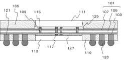
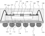
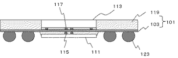
図1は、本実施形態に係る半導体装置の構成を模式的に示す断面図である。図1に示した半導体装置100は、平板状の配線体101と、配線体101の一方の面に設けられた第一の半導体素子113と、配線体101の第一の半導体素子113の設けられた側の面および第一の半導体素子113の側面を被覆する絶縁樹脂119と、配線体101の他方の面に、第二の半導体素子111に対向配置させて設けられた第二の半導体素子111と、を有する。
(First embodiment)
FIG. 1 is a cross-sectional view schematically showing the configuration of the semiconductor device according to the present embodiment. A
配線体101は、配線層103、シリコン層105および絶縁膜107がこの順に積層された構成である。第一の半導体素子113は配線層103に接して設けられ、第二の半導体素子111は絶縁膜107に接して設けられている。
The
配線層103は、平板状の絶縁体と、絶縁体を貫通する導電体と、を有する。導電体を介して第二の半導体素子111と第一の半導体素子113とが電気的に接続される。また、配線層103は、所定の形状および配置を有する配線を備える。配線層103は、単層であってもよいし、多層であってもよい。なお、配線層103の具体的な構成は、第三の実施形態および第七の実施形態において後述する構成とすることができる。
The
シリコン層105は、配線層103を支持する支持層である。シリコン層105の配線層103と反対側の面に設けられた絶縁膜107は、たとえばSiO2等の酸化膜、SiNやSiON等の窒化膜とする。
The
なお、配線層103の支持層として、本実施形態および以降の実施形態においてはシリコン層105を例示しているが、第一の半導体素子113および第二の半導体素子111の基板として通常用いられているSiと同程度の熱膨張率を有する他の材料とすることもできる。
In this embodiment and the following embodiments, the
支持層として、たとえば、線膨張係数が.0.5ppm/℃以上5ppm/℃以下の材料を用いることができる。線膨張係数を0.5ppm/℃以上とすることにより、半導体装置100の製造歩留まりを向上させることができる。また、5ppm/℃以下線膨張係数をとすることにより、第一の半導体素子113および第二の半導体素子111との電気的な接続信頼性を充分に確保することができる。また、支持層は、熱伝導性に優れた材料により構成するとよい。シリコン以外の支持層の材料として、具体的には、AlN等のセラミック材料や、パイレックス(登録商標)ガラス等の珪ホウ酸ガラス等が挙げられる。
As the support layer, for example, the linear expansion coefficient is. A material having a concentration of 0.5 ppm / ° C. to 5 ppm / ° C. can be used. By making the linear expansion coefficient 0.5 ppm / ° C. or higher, the manufacturing yield of the
また、配線層103は、シリコン層105および絶縁膜107を貫通して設けられた導体ヴィア109を有する。これにより、配線層103の両面の電気的導通が確保される。導体ヴィア109の平面配置に特に制限はなく、半導体装置100の設計に応じて適宜選択することができる。たとえば、導体ヴィア109を正方格子状に配置したり、千鳥配置等の斜格子状に配置したりすることができる。
In addition, the
第一の半導体素子113は、配線体101の配線層103の側にアンダーフィル樹脂127を介して接合されている。第一の半導体素子113中の導電部材(不図示)はアンダーフィル樹脂127中に埋設された電極117を介して導体ヴィア109にフリップチップ接続されている。また、配線体101において、第一の半導体素子113が設けられている側の面には、第一の半導体素子113の側壁を覆う絶縁樹脂119が設けられている。
The
第一の半導体素子113および第二の半導体素子111の構成は、半導体装置100の設計に応じて適宜選択することができるが、たとえば、第一の半導体素子113をメモリLSIチップとし、第二の半導体素子111をロジックLSIチップとすることができる。
The configurations of the
封止樹脂である絶縁樹脂119の材料に特に制限はなく、半導体封止用の樹脂を適宜選択して用いることができる。たとえば、シリカやアルミナ等の無機充填剤を含むエポキシ樹脂とすることができる。
There is no particular limitation on the material of the insulating
導体スルーホール121は、絶縁樹脂119を貫通し、配線体101中の導電体に電気的に接続されている。導体スルーホール121の配線体101と反対側の面は絶縁樹脂119から露出しており、露出面に電極端子123が設けられている。導体スルーホール121は電極端子123を介して外部に電気的に接続されている。
The conductor through
第二の半導体素子111は、配線体101の絶縁膜107の側にアンダーフィル樹脂127を介して接合されている。第二の半導体素子111中の導電部材(不図示)は、アンダーフィル樹脂125中に埋設された電極115を介して導体ヴィア109にフリップチップ接続されている。
The
半導体装置100において、第一の半導体素子113と第二の半導体素子111とは、電極117、配線層103中の導電体、導体ヴィア109および電極115を介して電気的に接続された構成となっている。なお、本実施形態および以降の他の実施形態において、電極115および電極117は、たとえばバンプとすることができる。
In the
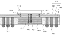
次に、図1に示した半導体装置100の製造方法を説明する。半導体装置100は、シリコン基板上で配線層103が形成され、配線層103上に前記第一の半導体素子113が接続され、第一の半導体素子113の側面および第一の半導体素子113の露出面が樹脂封止された後に、シリコン基板を除去することにより得られる。図2(a)〜図2(c)、図3(a)〜図3(c)、および図4(a)〜図4(c)は、半導体装置100の製造工程を示す断面図である。
Next, a method for manufacturing the
まず、図2(a)に示すように、ウェハ状態のシリコン基板133の上部に絶縁膜107を介してシリコン層105が形成された、SOI(シリコンオンインシュレータ)基板129を準備する。絶縁膜107は単層であってもよいし、多層であってもよい。
First, as shown in FIG. 2A, an SOI (silicon on insulator)
次に、SOI基板129の導体ヴィア109を設ける位置に、シリコン層105および絶縁膜107を貫通する開口部を形成する。そして、開口部が設けられたSOI基板129の表面に拡散防止膜を形成する。これにより、導体ヴィア109を構成する材料のSOI基板中への拡散を抑制することができる。そして、開口部を導電材料により埋め込むことにより、導体ヴィア109を形成する(図2(b))。導体ヴィア109は、SOI基板129において第二の半導体素子111および第一の半導体素子113が接合される領域に設けることができる。
Next, an opening that penetrates the
導体ヴィア109の材料としては、たとえば、銅、アルミニウム、タングステン等の金属や多結晶シリコンなどを用いることができる。なお、導体ヴィア109が絶縁膜107を貫通せずに、シリコン層105から絶縁膜107中の所定の位置にわたって設けられた構成としてもよい。また、導体ヴィア109がシリコン層105を貫通し絶縁膜107の上部に接する構成であってもよい。
As a material of the conductor via 109, for example, a metal such as copper, aluminum, tungsten, or polycrystalline silicon can be used. Note that the conductor via 109 may be provided from the
次に、SOI基板129の上部に配線層103を形成する(図2(c))。配線層103の作製方法は、第三または第七の実施形態で後述する方法とすることができる。また、シリコン層105上に絶縁膜を形成し、たとえばダマシン法により所定の形状の配線を所定の位置に配置してもよい。配線は、導体ヴィア109に電気的に接続される。配線の材料は、導体ヴィア109の材料と同じ材料としてもよいし、異なる導電材料としてもよい。配線層103は単層構造であっても多層構造であっても構わない。また、配線層103を形成する前に、シリコン層105上にトランジスタ等の能動素子やメモリ素子等の受動素子など、所定の素子を形成してもよい。
Next, the
次に、配線層103上に、図1における導体スルーホール121となる導体ポスト131を形成する(図3(a))。導体ポスト131の材料は、たとえば銅または金などの金属とすることができる。また、導体ポスト131は、配線層103上に、導体ポスト131を設ける領域を開口部とするレジストパターンを設け、たとえばセミアディティブ法の無電解めっき法により、開口部中に金属膜を成長させることにより作製することができる。
Next, a
次に、配線層103上に第一の半導体素子113を電気的に接続する。接続方法としては各種の方法を用いることが可能であるが、たとえば、第一の半導体素子113上にあらかじめ形成した電極117としてバンプ電極を形成しておき、電極117と配線層103中の配線とをバンプ接合することにより接続することができる。このとき、フリップチップ接合法を用いることができる。フリップチップ接合法を用いることにより、配線層103と第一の半導体素子113とを簡便な方法で確実に接続することができる。また、他の接続方法としては、たとえば、配線層103の表面と第一の半導体素子113の表面をプラズマ照射などの方法で活性化した状態で押圧接合する、活性化接合法などが挙げられる。接合後、第一の半導体素子113とSOI基板129との間にアンダーフィル樹脂127を充填する(図3(b))。
Next, the
そして、トランスファーモールドなどの方法を用いて、配線層103の上面全面を絶縁性の絶縁樹脂119で封止する(図3(c))。これにより、第一の半導体素子113および導体ポスト131は絶縁樹脂119中に埋設される。封止方法としてはこの他にも絶縁樹脂シートを圧着する方法や、液状樹脂を塗布後、硬化させる方法など各種の方法から選択することができる。
Then, the entire upper surface of the
次に、絶縁樹脂119の形成面側の研削等により絶縁樹脂119を薄化して、第一の半導体素子113の上面および導体ポスト131の端部を露出させる(図4(a))。なお、この工程は、後述するシリコン基板133の除去工程(図4(b))の後に行うこともできる。また、図3(c)を用いて前述した絶縁樹脂119の形成工程において絶縁樹脂119の膜厚をあらかじめ所定の厚さにコントロールすることも可能であり、その場合、導体ポスト131の露出工程の省略が可能となる。
Next, the insulating
そして、第一の半導体素子113の接合面の裏面の側からシリコン基板133を除去する。このとき除去方法としては、機械研削、CMP、ケミカルエッチングなどを採用することができる。また、別の除去方法として、シリコン基板133と配線層103との界面に密着力の低い層をあらかじめ形成しておき、この介在層の部分から剥離させるなどの方法が挙げられる。さらに、絶縁膜107の一部や拡散防止膜(不図示)を除去し、導体ヴィア109の端面を露出させる(図4(b))。導体ヴィア109を露出させるプロセスに特に限定はなく、各種の方法が選択可能である。
Then, the
次に、露出した導体ヴィア109に第二の半導体素子111を接続する。接続方法として、第一の半導体素子113の接続(図3(b))の方法を用いることができる。たとえば、第二の半導体素子111の表面に電極115を形成し、シリコン層105と導体ヴィア109とを接合することにより接続できる。接続後、第二の半導体素子111とSOI基板129との間にアンダーフィル樹脂127を充填してもよい(図4(c))。
Next, the
そして、導体ポスト131の露出面にはんだバンプなどの電極端子123を形成する。以上の工程により、図1に示した半導体装置100が製造可能される。以上のプロセスは初期的にはウェハすなわちシリコン基板133上に第二の半導体素子111および第一の半導体素子113がそれぞれ複数設けられた半導体装置の状態で実施されるが、絶縁樹脂119による封止工程以降、任意の位置で複数のチップに半導体装置間を分離することが可能である。また、前述したように、工程の順序としても、シリコン基板133除去と絶縁樹脂119の研削順序を逆にすることなどの変更が可能である。
Then,
次に、図1に示した半導体装置100の効果を説明する。
図1に示した半導体装置100において、配線体101は、絶縁膜107、シリコン層105および配線層103がこの順に積層された構造になっている。そして、配線層103中の導電体およびこれに接続して設けられた導体ヴィア109により構成される貫通電極が配線体101を貫通した構成となっている。また、配線体101の両面に第一の半導体素子113および第二の半導体素子111が対向して接合されている。
Next, the effect of the
In the
支持層となるシリコン層105を設けることにより、熱膨張係数の相違による反りの発生、接合精度の低下や残留熱応力による接続信頼性の低下を抑制することができる。このため、高精度で信頼性の高い接続が可能となる。また、高密度で導体ヴィア109を配置した場合にも、確実に配線体101と第一の半導体素子113および第二の半導体素子111とを接続することができる。このため、配線体101を貫通する貫通電極構造の高密度配置が可能となる。なお、配線体101を貫通する貫通電極構造は、複数の導電体からなる構成とすることができる。
By providing the
また、支持層としてシリコン層105を有する配線体101の両面に、熱膨張係数の等しいシリコンデバイスすなわち第二の半導体素子111および第一の半導体素子113が接続される。このため、半導体装置100は構造の対称性に優れる。よって、半導体装置100は製造安定性に優れ、第一の半導体素子113と第二の半導体素子111とを確実に接続する構成となっている。
Also, silicon devices having the same thermal expansion coefficient, that is, the
このように、半導体装置100では、配線体101の両面に設けられた第一の半導体素子113および第二の半導体素子111の間を高密度かつ優れた信頼性で接続することができる。半導体素子との接続信頼性の向上が可能なシリコン層105を有する配線体101を用いることで、高い配線密度で複数のチップや大規模なチップ間を接続することが可能となる。
Thus, in the
たとえば、半導体装置100は、たとえば50μm以下の電極ピッチ間隔すなわち導体ヴィア109の最小間隔がたとえば50μm以下である構成にも対応可能な構成となっている。また、高密度な配線体101を介した接続構造が実現されるため、チップサイズや電極位置、外部端子への配線接続に関する設計に対して高い自由度を提供し、発熱の大きいロジックLSIチップを第二の半導体素子111とすれば、ロジックLSIチップに対してヒートスプレッダなどの放熱機構を付加することも可能になる。
For example, the
また、半導体装置100において、平板状の配線体101の両面に接続された複数の半導体素子が配線体101を貫通する導体ヴィア109および導体ヴィア109に接続している配線層103中の配線を介して電気的に接続される。第一の半導体素子113および第二の半導体素子111が、シリコン層105と絶縁膜107とを貫通する導体スルーホールである導体ヴィア109および配線層103中の配線を介して電気的に接続されているため、第一の半導体素子113と第二の半導体素子111との接続距離を短くすることができる。このため、第一の半導体素子113と第二の半導体素子111との間の通信処理速度を増加させることができる。
Further, in the
また、複数のLSI間を微細な配線で高密度に接続することにより、電気特性に優れた構成となっている。また、従来のチップオンチップ(COC)構造の半導体装置などのマルチチップパッケージに比較して高い設計自由度を有する。これに伴い、放熱性に優れた構造も容易に実現可能である。さらには、2次実装信頼性も高いBGA型半導体装置とすることができる。さらにこのようにして高精度で接合された第一の半導体素子113を含む配線体101の片面を樹脂封止した後にシリコン基板133を取り除き、反対面に第二の半導体素子111を接続することにより、半導体素子間を高密度に電気的に接続することが可能になる。
In addition, by connecting the plurality of LSIs with fine wiring with high density, the structure has excellent electrical characteristics. In addition, it has a higher degree of design freedom than a multi-chip package such as a conventional semiconductor device having a chip-on-chip (COC) structure. Accordingly, a structure with excellent heat dissipation can be easily realized. Furthermore, a BGA type semiconductor device with high secondary mounting reliability can be obtained. Further, after sealing one side of the
また、半導体装置100では、半導体素子間を高密度に電気的に接続することが可能になるため、バス幅の拡大に相当する効果が得られる。このため、高速化と低消費電力化の両立が可能となる。たとえば、同一の処理速度でのクロック周波数の低減が可能となる。また、同一のクロック周波数における処理速度を増加させることができる。
In the
したがって、たとえば、半導体装置100は、大容量メモリとシステムLSIとのチップオンチップ接続に適用することができる。このとき、バンプ接続等の電極接続の多ピン化および狭ピッチ化が可能となる。また、配線体101は、ロジック回路が形成された半導体チップとDRAM等のメモリ素子が設けられたメモリチップとの間に設けられ、これらを接続する接続部材として好適に用いることができる。
Therefore, for example, the
また、半導体装置100において、配線体101の少なくとも片面に絶縁樹脂119からなる層が形成されている。具体的には、配線体101の配線層103の側の面には絶縁樹脂119の層が形成されている。また、絶縁樹脂119を貫通し、配線層103中の配線に接続された導体スルーホール121の絶縁樹脂119からの露出面に電極端子123が形成されている。樹脂貫通スルーホールである導体スルーホール121を用いた構造とすることにより、熱応力緩和機能により優れた二次実装信頼性が得られる。
In the
また、半導体装置100において、平板状の配線体101は、シリコン基板133上で形成される。半導体素子間を電気的に接続するための配線体101を剛性の高いシリコン基板133上で形成するため、配線パターンの微細化が可能となる。
In the
また、半導体装置100は、シリコン基板133上に配線体101が設けられ、配線体101上に第一の半導体素子113を接合した後シリコン基板133を除去することにより得られる。シリコン基板133を用いることにより、第一の半導体素子113と配線体101中の導電部材との接続プロセスにおける熱膨張係数の不一致による接続安定性の低下を抑制することができる。このため、非常に高精度で信頼性の高い接合が実現される。
Further, the
また、半導体装置100は、シリコン基板133を取り除いた後、反対面にもLSIすなわち第二の半導体素子111を接続することにより作製される。このように、半導体装置100は、複数のLSI間を微細な配線で高密度にかつ安定に接続された構成となっているため、従来のシステムインパッケージ(SiP)で実現できなかった良好な動作特性を発揮することができる。
The
なお、図1に示した半導体装置100および以降の実施形態に記載の半導体装置において、第一の半導体素子113が絶縁樹脂119に埋設されている構成とすることもできる。図5は、第一の半導体素子113が絶縁樹脂119中に埋設された構成の半導体装置を模式的に示す断面図である。
Note that in the
また、図1に示した半導体装置100および以降の実施形態に記載のシリコン層105を有する半導体装置において、支持層であるシリコン層105にトランジスタ等の能動素子が形成されていてもよい。こうすれば、配線体101をさらに高機能化することができる。
In the
また、半導体装置100および以降の実施形態に記載の半導体装置において、配線体101の第二の半導体素子111の接合された側の面にも絶縁樹脂が設けられていてもよい。図6は、第二の半導体素子111の側壁および絶縁膜107の表面を覆う絶縁樹脂135が設けられているフリップチップ型の半導体装置の構成を模式的に示す断面図である。配線体101の両面が絶縁樹脂119および絶縁樹脂135により封止された構成とすることにより、半導体装置の強度を向上させることができる。また、配線体101の両面の構成の対称性を高めることができるため、製造安定性を向上させることができる。
In the
以下の実施形態においては、第一の実施形態と異なる部分を中心に説明する。 In the following embodiment, it demonstrates centering on a different part from 1st embodiment.
(第二の実施形態)
第一の実施形態に記載の半導体装置100(図1)は、配線層103、シリコン層105、絶縁膜107がこの順に積層された構成の配線体101を備えていたが、配線体101は、配線層103およびシリコン層105の積層体からなる構成としてもよい。図7は、本実施形態に係る半導体装置110の構成を模式的に示す断面図である。
(Second embodiment)
The semiconductor device 100 (FIG. 1) described in the first embodiment includes the
図7に示した半導体装置110の基本構成は第一の実施形態に記載の半導体装置100(図1)と同様であるが、絶縁膜107が設けられておらず、第二の半導体素子111は配線体101のシリコン層105の表面に電極115およびアンダーフィル樹脂127を介して接続されている点が異なる。また、半導体装置110において、導体ヴィア109は、シリコン層105を貫通し配線層103中の配線に電気的に接続されている。
The basic configuration of the
半導体装置110は、図2(b)、図2(c)、図3(a)〜図3(c)、および図4(a)〜図4(c)を用いて前述した工程を用いて製造することができる。まず、シリコン基板133に導体ヴィア109を形成し、導体ヴィア109の形成面に配線層103を形成する。そして、第一の実施形態の場合と同様にして第一の半導体素子113および第二の半導体素子111を配線体101に接合する。なお、半導体装置110の製造においては、シリコン基板133を裏面から薄化し、除去せずに所定の厚さのシリコン基板133をシリコン層105として残存させる。
The
図7に示した半導体装置110においても、配線層103および支持層であるシリコン層105がこの順に積層された構成の配線体101を備えているため、第一の半導体素子113および第二の半導体素子111の接合時の熱膨張率差が小さい構成となっている。このため、これらの接続信頼性を充分に確保するとともに、接続する導体ヴィア109の間隔を充分に小さくすることができる。
The
また、半導体装置110においては、バルクのシリコン基板133が利用可能であり、シリコン基板133の研削厚をコントロールすることにより所定の厚さのシリコン層105を有する配線体101を設けることができる。このため、SOI基板129を用いる必要がなく、装置構成を簡素化することができる。
In the
なお、半導体装置110においては、導体ヴィア109の周囲におけるシリコン層105の表面が絶縁される。これにより、第二の半導体素子111の電極間の絶縁性が確保される。図7では、絶縁性のアンダーフィル樹脂125をシリコン層105と第二の半導体素子111との間に埋設することより、導体ヴィア109の周囲が絶縁された構造となっている。
In the
(第三の実施形態)
以上の実施形態に記載の半導体装置において、配線体101が配線層103のみから構成されていてもよい。図8は、本実施形態に係る半導体装置120の構成を模式的に示す断面図である。
(Third embodiment)
In the semiconductor device described in the above embodiment, the
図8に示した半導体装置120の基本構成は第一の実施形態に記載の半導体装置100(図1)と同様であるが、配線体101が配線層103のみからなり、第一の半導体素子113および第二の半導体素子111が配線層103の異なる面に対向して設けられている点が異なる。また、第二の半導体素子111が配線層103の表面に電極115およびアンダーフィル樹脂127を介して接続されている点が異なる。
The basic configuration of the
半導体装置120において、配線層103からなる配線体101は、たとえば以下の方法により製造することができる。図9(a)〜図9(c)および図10(a)〜図10(c)は、配線層103の作製工程を模式的に示す断面図である。
In the
まず、シリコン基板133の表面に、スパッタ法などを用いて金属のシード層137を形成する(図9(a))。シード層137は、たとえばNiとすることができる。次に、シード層137上に配線形成位置を露出させるレジストパターンを形成し、シード層137の露出部を起点として所定のパターンの接続電極139を形成する(図9(b))。接続電極139は、後述する絶縁樹脂膜141の下面側の電極である。接続電極139は、外部引き出し電極として用いることができる。接続電極139は、たとえば電解めっき法により形成することができる。
First, a
接続電極139の材料は、Cu、Al、Au、Ni、W等の金属や合金、メタルシリサイド、またはポリシリコンなどの各種導電性材料で形成することができ、単層構造の他、半田の拡散防止層や電極強度の補強層を含む積層構造とすることもできる。積層構造の電極としては、下端側からAu、Ni、Cuがこの順で積層された電極(Au/Ni/Cu電極)、下端側からNi、Au、Ni、Cuがこの順で積層された電極(Ni/Au/Ni/Cu電極)、このNi/Au/Ni/Cu電極から最下端層のNi層が除去されたAu/Ni/Cu電極、下端側からCu、Ag、Cuがこの順で積層された電極(Cu/Ag/Cu電極)を挙げることができる。上記電極において、中間のNi層は半田の拡散防止層として機能する。また、Cu/Ag/Cu電極において、Ag層は電極の強度を向上する補強層として機能する。
The material of the
次に、接続電極139の形成面の全面に絶縁樹脂膜141を設け、接続電極139を絶縁樹脂で埋め込む(図9(c))。絶縁樹脂膜141は、たとえばラミネートフィルム状の絶縁樹脂シートを接合する方法や、スピンコート法等により形成することができる。そして、絶縁樹脂膜141の所定の位置にレーザー光を照射し、レーザーヴィアすなわち開口部143を設ける(図10(a))。また、絶縁樹脂膜141に感光性樹脂を用い、フォトリソグラフィー法により開口部143を形成してもよい。
Next, an insulating
その後、開口部143をCu等の所定の金属膜で埋めこみ、ヴィアプラグ145とする(図10(b))。そして、ヴィアプラグ145に接続し、所定のパターンを有する配線147を絶縁樹脂膜141上に形成する(図10(c))。配線147の材料は、たとえばCu等の金属とする。そして、配線147の表面に、上層からAu/Niからなるめっき層(不図示)を形成する。以上の工程により、シリコン基板133上に多層の配線層103が形成される。
Thereafter, the
なお、ヴィアプラグ145の平面配置に特に制限はなく、半導体装置120の設計に応じて適宜選択することができる。たとえば、ヴィアプラグ145を正方格子状に配置したり、千鳥配置等の斜格子状に配置したりすることができる。
Note that the planar arrangement of the via
図8に示した半導体装置120は、以上の方法でシリコン基板133上に配線層103を作製した後、第二の実施形態に記載の半導体装置110(図7)の製造工程を用いて製造することができる。ここで、第二の実施形態においては配線体101がシリコン層105を有する構成であったため、シリコン基板133を薄化したが、本実施形態に係る半導体装置120はシリコン層105を有しない構成であるため、第一の半導体素子113を接合した後、第一の実施形態の場合と同様にシリコン基板133を除去する。そして、配線体101に第二の半導体素子111を接合する
The
こうして得られる半導体装置120(図8、図10(c))において、接続電極139は、絶縁樹脂膜141の第二の半導体素子111の側に設けられる。接続電極139は、第二の半導体素子111を第一の半導体素子113に接続するための素子接続電極と、第二の半導体素子111を外部に接続するための外部接続電極とを含む。接続電極139がこれらのいずれである場合においても、接続電極139の側面全面が絶縁樹脂膜141中に埋設されるとともに、接続電極139の絶縁樹脂119と反対側の面の全体が絶縁樹脂膜141から露出し、この面では接続電極139が絶縁樹脂膜141に接していない構成となっている。
In the semiconductor device 120 (FIGS. 8 and 10C) thus obtained, the
これにより、接続電極139の高密度配置が可能となる。また、接続電極139の側面外周を確実に絶縁することができる。また、配線層103の第二の半導体素子111の側の面を平坦面としつつ、電極端子123を所定の領域に確実に設け、電極端子123の周囲を確実に絶縁することが可能となる。
Thereby, the
また、接続電極139を外部接続電極とする場合、従来のワイヤボンディング形式の接続に対し、高密度かつ短い接続距離での接続が可能となる。
Further, when the
なお、半導体装置120において、接続電極139は、複数の導電部材が接合されて構成されていてもよい。また、接続電極139の絶縁樹脂膜141からの露出面は平坦面でなくてもよい。たとえば、接続電極139の露出面が絶縁樹脂膜141の表面から凸状にはりだした曲面であってもよい。また、接続電極139は、絶縁樹脂膜141からの露出面にバンプ電極が接合されていてもよい。
Note that in the
接続電極139の絶縁樹脂膜141からの露出面を曲面とすることにより、接続電極139を他の接続部材に接合するのに充分な高さが確保される。こうした構成は、たとえば接続電極139の露出面に、無電解めっき法などにより曲面状の電極を形成することにより得られる。
By making the exposed surface of the
また、図8に示した半導体装置120は、バルクのシリコン基板133を利用して製造することが可能である。このため、低コストで高密度な配線構造により第一の半導体素子113と第二の半導体素子111とを接続することができる。また、配線体101が配線層103からなるため、簡素な構成である。このため、製造工程を簡素化し、製造コストの低減が可能である。
In addition, the
第一の半導体素子113および第二の半導体素子111は、線膨張係数が0.5ppm/℃以上5ppm/℃以下の基板を有する構成とした場合、シリコン基板133との熱膨張係数の差を小さくすることができるため、配線体101と第一の半導体素子113および第二の半導体素子111との接続信頼性を向上させることができる。また、第一の半導体素子113および第二の半導体素子111の基板の種類に応じて、バルクのシリコン基板133に代えて、これらの半導体素子の基板との線膨張係数差の小さい材料を用いて半導体装置120を製造してもよい。
When the
また、第一の半導体素子113および第二の半導体素子111が、シリコン基板を有する素子であってもよく、この場合、バルクのシリコン基板133を用いることによる効果が顕著に発揮される。このため、第一の半導体素子113と第二の半導体素子111とを接続する導体ヴィア109を高密度で設け、これらの半導体素子間を高密度で接続することが可能となる。
In addition, the
また、配線層103中の接続電極139およびヴィアプラグ145の側面は絶縁樹脂膜141に覆われているため、接続電極139の端面に電極115または電極117として半田バンプを接続する場合、半田の流動による接続不良を抑制することができる。
Further, since the side surfaces of the
また、半導体装置120は、配線体101の両面に半導体素子が接合されるため、対称性が高い構成である。このため、第二の半導体素子111と第一の半導体素子113との接続信頼性を充分に確保することが可能となる。
In addition, the
また、第一の半導体素子113の配線層103の側の面と、第二の半導体素子111の配線層103の側の面とが、配線層103の面に略垂直に一直線に接続されている。このため、接続距離を短縮し、安定的な接続が確保された構成となっている。なお、配線体101の内部で水平方向に延在する配線を介さずに接続されていれば、半導体素子間の接続が完全に垂直でなくてもよい。また、本実施形態において、配線体101の面に垂直方向に設けられた導電部材すなわちヴィアプラグ145の最小間隔をたとえば50μm以下と高密度化することができる。
Further, the surface on the
本実施形態において、配線層103からなる配線体101を有する半導体装置は、以下の構成としてもよい。図31は、本実施形態に係る半導体装置の構成を模式的に示す断面図である。図31に示した半導体装置150の基本構成は図8に示した半導体装置120と同様であるが、絶縁樹脂119中を貫通する導体スルーホール121を有さず、配線体101の第二の半導体素子111の側の面に接して設けられ、配線体101中の配線に接続した電極端子123を有する点が異なる。
In the present embodiment, the semiconductor device having the
半導体装置150は、図8に示した半導体装置120と同様に、平板状の絶縁樹脂膜141およびこれを貫通する導電体を有するため、第一の半導体素子113と第二の半導体素子111とを高密度で確実に接続することができる。また、絶縁樹脂119中に導体スルーホール121を設ける工程を設けることなく製造可能であるため、製造プロセスを簡素化可能な構成となっている。
Like the
図32および図33は、図31に示した半導体装置150の配線層103の構成を詳細に示した断面図である。
32 and 33 are cross-sectional views showing in detail the configuration of the
図32に示した半導体装置では、配線層103が、ヴィアプラグ145およびパッド175が設けられた層と配線147が設けられた層との二層構造となっている場合を例示している。なお、ヴィアプラグ145およびパッド175が設けられた層には、ヴィアプラグ145およびパッド175以外の所定の配線が形成されていてもよい。
In the semiconductor device shown in FIG. 32, the case where the
図32において、電極端子123は、配線147に接合されている。また、配線147は、所定のヴィアプラグ145またはパッド175に接合されている
In FIG. 32, the
ヴィアプラグ145およびパッド175は、絶縁樹脂膜141の第二の半導体素子111に設けられた接続電極である。これらは、前述した図10(c)における接続電極139に相当する。これらの接続電極の側面全面が絶縁樹脂膜141中に埋設されるとともに、接続電極の絶縁樹脂119と反対側の面が全面絶縁樹脂膜141から露出し、この面では接続電極が絶縁樹脂膜141に接していない構成となっている。これにより、配線層103を平坦面としつつ、電極端子123を所定の領域に選択的に設けることが可能となる。
The via
なお、図32において、ヴィアプラグ145は第二の半導体素子111との素子接続電極であり、パッド175は電極端子123に接続する外部引き出しパッド、すなわち外部接続電極である。
In FIG. 32, a via
配線147は、絶縁樹脂膜141第一の半導体素子113の接続面上に設けられている。配線147の側面および絶縁樹脂119の側の面は、絶縁樹脂膜141に埋設されておらず、絶縁樹脂膜141から露出している。また、露出部分は絶縁樹脂119中に埋設されている。これにより、配線層103の強度が充分に確保されている。
The
なお、図32において、第一の半導体素子113をメモリチップとし、第二の半導体素子111をロジックチップとしてもよい。このとき、図31における電極115として、第二の半導体素子111を第一の半導体素子113に接続させるメモリ通信用電極179および第二の半導体素子111を電極端子123に接続させる外部入出力用電極183を設けることができる。また、図31における電極117として、第一の半導体素子113を第二の半導体素子111に接続させるメモリ電極181を設けることができる。
In FIG. 32, the
また、図33に示した半導体装置の基本構成は図32と同様であるが、図32と異なり、ヴィアプラグ145とパッド175とが異なる層に設けられている。このため、パッド175の層すなわち接続電極139の層、ヴィアプラグ145の層、および配線147の層がこの順に積層された配線層103は、図32よりも一層多い三層構造となっている。この構成では、接続電極139を有する層が一つの面が絶縁樹脂膜141から露出した接続電極の層となっている。接続電極139の一部は第二の半導体素子111に接続する素子接続電極であり、他の一部は電極端子123に接続するパッド175である。
The basic structure of the semiconductor device shown in FIG. 33 is the same as that of FIG. 32, but unlike FIG. 32, the via
また、図33において、第二の半導体素子111をメモリチップとし、第一の半導体素子113をロジックチップとしてもよい。このとき、図32の場合とは逆に、図31の電極115としてメモリ電極181を設け、図31の電極117としてメモリ通信用電極179および外部入出力用電極183を設けることができる。
In FIG. 33, the
なお、図31に示した半導体装置150において、配線層103の構成および積層数は図32および図33に示した態様に限られず、装置構成に応じて適宜設定することができる。また、図32および図33に示した半導体装置における配線層103は、たとえば第七の実施形態にて後述する方法により製造することができる。
In the
さらに、本実施形態に係る半導体装置は、他の半導体装置と積層接続して用いることもできる。図34および図35は、こうした半導体装置の構成を模式的に示す断面図である。 Furthermore, the semiconductor device according to the present embodiment can be used in a stacked connection with other semiconductor devices. 34 and 35 are cross-sectional views schematically showing the configuration of such a semiconductor device.
図34は、図8に示した半導体装置120を他の半導体装置185と接続した構成を示す図である。半導体装置120と半導体装置185とは、半導体装置185に設けられた電極端子および半導体装置120に設けられた導体スルーホール121を介して接続されている。
FIG. 34 is a diagram illustrating a configuration in which the
また、図35は、図31に示した半導体装置150を他の半導体装置187と接続した構成を示す図である。半導体装置150と半導体装置187とは、半導体装置150に設けられた電極端子123および半導体装置187に設けられた導体スルーホールを介して接続されている。
FIG. 35 is a diagram illustrating a configuration in which the
なお、本実施形態において、配線層103からなる配線体101の構成を第七の実施形態において後述する構成としてもよい。また、第七の実施形態に記載の半導体装置に本実施形態の構成を適用することもできる。
In the present embodiment, the configuration of the
(第四の実施形態)
第一の実施形態に記載の半導体装置100において、配線体101の配線層103の側に接合された第一の半導体素子113が、複数の半導体素子の積層体であってもよい。図11は、本実施形態に係る半導体装置の構成を模式的に示す断面図である。図11に示した半導体装置の基本構成は第一の実施形態に記載の半導体装置100(図1)と同様であるが、第一の半導体素子113に代えて複数の半導体素子149が面の法線に沿って積層された構成である点が異なる。
(Fourth embodiment)
In the
図11に示した半導体装置において、配線体101の配線層103の面に、アンダーフィル樹脂127、半導体素子149、アンダーフィル樹脂127、半導体素子149、・・・、アンダーフィル樹脂127、半導体素子149が繰り返し設けられた構成によって複数の半導体素子149が積層されている。それぞれの半導体素子149には、当該半導体素子149を貫通する導体スルーホール151が設けられている。また、それぞれのアンダーフィル樹脂127には隣接する二つの半導体素子149間を接続する電極117が設けられている。
In the semiconductor device shown in FIG. 11, an
図11に示した半導体装置は、絶縁樹脂119の形成面側に複数の積層された半導体素子149が接続され、積層された半導体素子149間が、半導体素子149を貫通する導体スルーホール151を介して電気的に接続されている構成になっている。具体的には、複数の半導体素子149は、配線層103に接続する電極117、導体スルーホール151、電極117、導体スルーホール151、・・・、電極117という電極117と導体スルーホール151の繰り返し構造により配線体101に電気的に接続される。電極117と導体スルーホール151との繰り返し構造は、配線体101の表面に対する法線方向に略一直線上に形成されている。このため、図11に示した半導体装置は、半導体素子149間の接続距離が短く、接続信頼性に優れた構成となっている。
In the semiconductor device illustrated in FIG. 11, a plurality of stacked
また、図11では、配線層103の側に半導体素子149の積層体が配置されたが、配線体101の絶縁膜107の側の面に接続される第二の半導体素子111が複数の半導体素子の積層構造を有していてもよい。図12は、こうした半導体素子の構成を模式的に示す断面図である。図12に示した半導体装置の基本構成は第一の実施形態に記載の半導体装置100(図1)と同様であるが、第二の半導体素子111に代えて複数の半導体素子149が面の法線に沿って積層された構成である点が異なる。
In FIG. 11, the stacked body of the
図12に示した半導体装置において、配線体101の絶縁膜107の面に、アンダーフィル樹脂125、半導体素子149、アンダーフィル樹脂125、半導体素子149、・・・、アンダーフィル樹脂125、半導体素子149が繰り返し設けられた構成によって複数の半導体素子149が積層されている。それぞれの半導体素子149には、当該半導体素子149を貫通する導体スルーホール151が設けられている。また、それぞれのアンダーフィル樹脂125には隣接する二つの半導体素子149を接続する電極115が設けられている。
In the semiconductor device shown in FIG. 12, the
また、複数の半導体素子149は、絶縁膜107に接続する電極115、導体スルーホール151、電極115、導体スルーホール151、・・・、電極115という電極115と導体スルーホール151の繰り返し構造により配線体101に電気的に接続される。電極115と導体スルーホール151との繰り返し構造は、配線体101の表面に対する法線方向に略一直線上に形成されている。このため、図12に示した半導体装置も、図11に示した半導体素子の場合と同様に、半導体素子149間の接続距離が短く、接続信頼性に優れた構成となっている。
In addition, the plurality of
なお、第一の半導体素子113または第二の半導体素子111が複数の半導体素子149の積層体からなる構成は、第二および第三の実施形態に記載の配線体101の構成に適用することもできる。
The configuration in which the
また、本実施形態および積層された半導体素子149を有する他の実施形態の半導体装置において、積層された半導体素子149は、積層メモリモジュールとすることができる。これにより、メモリ容量を増加させつつ、ロジック部等を有する第二の半導体素子111との良好な電気的接続を得ることができる。
In the semiconductor device of this embodiment and another embodiment having the stacked
(第五の実施形態)
以上の実施形態に記載の半導体装置において、配線体101の一つの面に複数の半導体素子が平面配置されていてもよい。以下、第四の実施形態に記載の半導体装置(図11)の場合を例に説明する。図13は、本実施形態に係る半導体装置の構成を模式的に示す断面図である。
(Fifth embodiment)
In the semiconductor device described in the above embodiment, a plurality of semiconductor elements may be arranged in a plane on one surface of the
図13に示した半導体装置の基本構成は図11に示した半導体装置の構成と同様に、配線体101の絶縁樹脂119形成面側、すなわち配線層103側の面に、複数の積層された半導体素子149が接続され、積層された半導体素子149間が、半導体素子149を貫通する導体スルーホール151および電極117を介して電気的に接続されている。また、図13に示した半導体装置では、図11に示した半導体装置と異なり、配線体101の絶縁樹脂119形成面に対向する面、すなわち絶縁膜107側の面に、複数の第二の半導体素子111が配設されている点が異なる。
The basic configuration of the semiconductor device illustrated in FIG. 13 is similar to the configuration of the semiconductor device illustrated in FIG. 11. A plurality of stacked semiconductors are formed on the insulating
図13に示した半導体装置においては、複数の第二の半導体素子111が同一平面に配置されて、これらが電極117および導体ヴィア109を介して配線層103に接続する構成となっている。このため、複数の第二の半導体素子111と配線層103との接続距離をそろえ、これらを短縮することができる。よって、複数の第二の半導体素子111と半導体素子149との接続信頼性に優れた構成となっている。また、シリコン層105に形成する導体ヴィア109を高密度化することが可能であるため、第二の半導体素子111を高密度で確実に配線層103に接続することができる。
In the semiconductor device shown in FIG. 13, a plurality of
(第六の実施形態)
以上の実施形態に記載の半導体装置において、配線体101中に設けられている導体ヴィア109を導体ワイヤとの接続部材として利用することもできる。また、配線体101の絶縁樹脂119形成面と対向する面に接着材により積層された複数の半導体素子が接続され、そのうち少なくとも1つの半導体素子が、ワイヤを介して、配線体101に電気的に接続された構成とすることができる。図14は、本実施形態に係る半導体装置の構成を模式的に示す断面図である。
(Sixth embodiment)
In the semiconductor device described in the above embodiment, the conductor via 109 provided in the
図14に示した半導体装置の基本構成は第一の実施形態に記載の半導体装置(図6)と同様であるが、第一の半導体素子113および第二の半導体素子111が設けられていない領域においても配線体101のシリコン層105および絶縁膜107を貫通する導体ヴィア109が設けられている点が異なる。
The basic configuration of the semiconductor device shown in FIG. 14 is the same as that of the semiconductor device described in the first embodiment (FIG. 6), but the region where the
また、図14に示した半導体装置においては、配線体101の絶縁樹脂119形成面と対向する面すなわち絶縁膜107の側の面に、接着剤153により積層された複数の第二の半導体素子111が接続されている。そして、少なくとも1つの第二の半導体素子111が、配線体101のシリコン層105と絶縁膜107を貫通する導体ヴィア109に接続して形成された導体パッド159に、導体パッド157および導体からなるワイヤ155を介して接続された構成となっている。導体パッド157は、たとえば無電解めっき法により形成することができる。
In the semiconductor device shown in FIG. 14, a plurality of
本実施形態では、導体ヴィア109を第一の半導体素子113および第二の半導体素子111の接合領域以外の絶縁樹脂119および絶縁樹脂135に封止された領域にも設けることにより、第二の半導体素子111とのワイヤボンディングに好適に利用することができる。このため、第二の半導体素子111と配線体101との電気的接続の設計の自由度の大きい構成となっている。
In the present embodiment, the conductor via 109 is provided also in a region sealed with the insulating
(第七の実施形態)
図15(a)および図15(b)は、本実施形態に係る半導体装置の構成を模式的に示す断面図である。図15(a)は、図15(b)に示した半導体装置のボンディング前の状態を示す図である。図15(a)に示した半導体装置は、第三の実施形態に記載の配線層103からなる配線体101の一方の面に第一の半導体素子113が接合され、他方の面に第二の半導体素子111が配設された構成を有する。第一の半導体素子113は、配線体101上を覆う絶縁樹脂119中に埋設されている。なお、絶縁樹脂119を貫通する導体スルーホール121および導体スルーホール121に接続する電極端子123は、図15(a)においては設けられていない。
(Seventh embodiment)
FIG. 15A and FIG. 15B are cross-sectional views schematically showing the configuration of the semiconductor device according to the present embodiment. FIG. 15A is a diagram showing a state before bonding of the semiconductor device shown in FIG. In the semiconductor device shown in FIG. 15A, the
図15(a)に示した半導体装置は、チップ間が電気的に接続された半導体モジュールである。図15(b)に示したように、図15(a)に示した半導体装置は、接着剤153によりヒートスプレッダ171の表面に接着される。半導体装置の側方においてヒートスプレッダ171の表面にサポートリング161およびTABテープ基板163がこの順に接着剤153により接着されている。TABテープ基板163の表面には配線層165が設けられている。配線層165は、端部が配線層103に向かって引き出されたインナーリード169を有し、インナーリード169はインナーリード封止樹脂167により封止されている。そして、図15(a)に示した半導体装置の外部に引き出された配線層103からなる配線体101は、TAB(Tape Automated Bonding)技術によりインナーリード169を介してTABテープ基板163上の配線層165に接続されている。
The semiconductor device shown in FIG. 15A is a semiconductor module in which chips are electrically connected. As shown in FIG. 15B, the semiconductor device shown in FIG. 15A is bonded to the surface of the
このように、配線層103を有する半導体装置は、TAB接続型の装置に適用することもできる。TAB技術を用いてインナーリードを接続することにより、半導体装置の設計の自由度をさらに増すことができる。
As described above, the semiconductor device including the
なお、本実施形態および配線層103からなる配線体101を有する他の実施形態に係る半導体装置において、配線体101の両面に第一の半導体素子113および第二の半導体素子111が接合された半導体モジュールの構成は、たとえば以下のようにすることができる。図16は、本実施形態に係る半導体モジュールの構成を模式的に示す断面図である。
In the semiconductor device according to this embodiment and another embodiment having the
図16に示した半導体モジュールは、図32に示した配線層103と同様の基本構成を有する配線体101を備える。接続電極であるヴィアプラグ145と外部引き出し用のパッド175とが同層に設けられている。また、これらと同層に樹脂止めパターン177が設けられている。樹脂止めパターン177は、ヴィアプラグ145やパッド175と同じ材料で同一工程により形成することができる。
The semiconductor module shown in FIG. 16 includes a
パッド175は、第一の半導体素子113および第二の半導体素子111の形成領域の側方における配線層103に設けられている。また、樹脂止めパターン177は、アンダーフィル樹脂125およびアンダーフィル樹脂127の形成領域の近傍において、これらのアンダーフィル樹脂の形成領域の側方に設けられている。
The
また、絶縁樹脂119の形成面と反対側の面に接続された第二の半導体素子111(ロジックLSIチップ)は、外部入出力用電極183、ヴィアプラグ145および配線147を介して配線147に接続されている。また、第二の半導体素子111は、メモリ通信用電極179が、ヴィアプラグ145、配線147およびメモリ電極181を介して配線層103の反対面に接続された第一の半導体素子113(メモリLSIチップ)と接続されている。
The second semiconductor element 111 (logic LSI chip) connected to the surface opposite to the surface on which the insulating
図16に示した半導体モジュールは、たとえば第三の実施形態に記載の方法(図9(a)〜図9(c)、図10(a)〜図10(c))を用いて作製することができる。また、以下の方法により作製してもよい。図21(a)〜図21(c)、図22(a)〜図22(c)、および図23は、図16に示した半導体モジュールの別の製造工程を模式的に示す断面図である。 The semiconductor module shown in FIG. 16 is manufactured using, for example, the method described in the third embodiment (FIGS. 9A to 9C and FIGS. 10A to 10C). Can do. Moreover, you may produce with the following method. 21 (a) to 21 (c), 22 (a) to 22 (c), and 23 are cross-sectional views schematically showing another manufacturing process of the semiconductor module shown in FIG. .
まず、シリコン基板133の表面に、スパッタ法などを用いて金属のシード層137を形成する(図21(a))。シード層137は、たとえばCuやNi等とすることができる。次に、シリコン基板133におけるシード層137の形成面の全面に絶縁樹脂膜141を設け、絶縁樹脂膜141の所定の位置にレーザー光を照射し、レーザーヴィアすなわち開口部143を設ける(図21(b))。
First, a
その後、開口部143をCu等の所定の金属膜で埋めこみ、ヴィアプラグ145等の接続電極とする(図21(c))。接続電極の材料は、Cu、Ni、Au、W等の金属または合金等の導電材料とすることができる。さらに具体的には、接続電極を、上からCu/Ni/Au/Niの4層構造とすることができる。また、上からCu/Ni/Auの3層構造とすることもできる。
Thereafter, the
そして、接続電極に接続し、所定のパターンを有する配線147を絶縁樹脂膜141上に形成する(図22(a))。配線147の材料は、たとえばCu等の金属とする。そして、配線147の表面に、上層からAu/Niからなるめっき層(不図示)を形成する。以上の工程により、シリコン基板133上に配線層103が形成される。
Then, a
次に、第二の実施形態に記載の半導体装置110(図7)の製造工程を用いて第一の半導体素子113を配線体101の表面に接続する。第一の半導体素子113のメモリ電極181と配線層103の配線147とを接合させて、第一の半導体素子113と配線層103との間にアンダーフィル樹脂127を充填する(図22(b))。そして、配線層103の表面全面に絶縁樹脂119を成形し、第一の半導体素子113をモールド封入する(図22(c))。
Next, the
そして、裏面研削等により、シリコン基板133を除去し、シード層137およびNi層をエッチング除去する。さらに、絶縁樹脂119の一部を研削し、ヴィアプラグ145の表面を露出させる(図23)。そして、配線体101の面に第一の半導体素子113に対向させて第二の半導体素子111を接続する。こうして、図16に示した半導体モジュールが得られる。
Then, the
また、図24は、図16に示した半導体モジュールの変形例である。図24に示した半導体モジュールの基本構成は図16と同様であるが、配線体101への第二の半導体素子111および第一の半導体素子113の接合面が反転している。この構成では、たとえば、第一の半導体素子113をロジックLSIチップとし、第二の半導体素子111をメモリチップとすることができる。
FIG. 24 shows a modification of the semiconductor module shown in FIG. The basic configuration of the semiconductor module shown in FIG. 24 is the same as that of FIG. 16, but the bonding surfaces of the
また、本実施形態において、配線層103からなる配線体101を有する半導体モジュールの構成は、図25または図29に示す構成としてもよい。図25および図29は、本実施形態に係る半導体モジュールの構成を模式的に示す断面図である。図25および図29に示した半導体モジュールは、それぞれ基本構成を図16および図24に示した半導体モジュールと同様としているが、配線層103が、接続電極139の形成層、ヴィアプラグ145の形成層、および配線147の形成層の三層の積層構造となっている点が異なる。接続電極139の一部は素子接続電極であり、他の一部は外部接続電極であるパッド175となっている。
In the present embodiment, the configuration of the semiconductor module having the
また、図25に示した構成では、たとえば、第一の半導体素子113をメモリチップとし、第二の半導体素子111をロジックLSIチップとすることができる。また、図29に示した半導体モジュールの基本構成は図25と同様であるが、配線体101への第二の半導体素子111および第一の半導体素子113の接合面が反転している。この構成では、たとえば、第一の半導体素子113をロジックLSIチップとし、第二の半導体素子111をメモリチップとすることができる。
In the configuration shown in FIG. 25, for example, the
図25に示した半導体モジュールは、たとえば次のようにして作製される。図26(a)〜図26(c)、図27(a)〜図27(c)および図28(a)〜図28(b)は、図25に示した半導体モジュールの製造工程を模式的に示す断面図である。 The semiconductor module shown in FIG. 25 is manufactured as follows, for example. 26 (a) to 26 (c), 27 (a) to 27 (c) and 28 (a) to 28 (b) schematically illustrate the manufacturing process of the semiconductor module shown in FIG. FIG.
まず、シリコン基板133の表面に、スパッタ法などを用いて金属のシード層137を形成する(図26(a))。次に、シード層137上に配線形成位置を露出させるレジストパターンを形成し、シード層137の露出部を起点として所定のパターンの接続電極139を形成する(図26(b))。
First, a
次に、接続電極139の形成面の全面に絶縁樹脂膜141を設け、接続電極139を絶縁樹脂で埋め込む(図26(c))。絶縁樹脂膜141は、たとえばラミネートフィルム状の絶縁樹脂シートを接合する方法や、スピンコート法等により形成することができる。シリコン基板133におけるシード層137の形成面の全面に絶縁樹脂膜141を設け、絶縁樹脂膜141の所定の位置にレーザー光を照射し、レーザーヴィアすなわち開口部143を設ける(図26(c))。
Next, an insulating
その後、開口部143をCu等の所定の金属膜で埋めこみ、ヴィアプラグ145とする(図27(a))。ヴィアプラグ145の材料は、たとえばCu等の金属とすることができる。また、ヴィアプラグ145は、たとえばめっき法により形成することができる。
Thereafter, the
そして、ヴィアプラグ145に接続し、所定のパターンを有する配線147を絶縁樹脂膜141上に形成する(図27(b))。配線147の材料は、たとえばCu等の金属とする。そして、配線147の表面に、上層からAu/Niからなるめっき層(不図示)を形成する。以上の工程により、シリコン基板133上に配線層103が形成される。
Then, a
次に、第二の実施形態に記載の半導体装置110(図7)の製造工程を用いて第一の半導体素子113を配線体101の表面に接続する。第一の半導体素子113のメモリ電極181と配線層103の配線147とを接合させて、第一の半導体素子113と配線層103との間にアンダーフィル樹脂127を充填する(図27(c))。そして、配線層103の表面全面に絶縁樹脂119を成形し、第一の半導体素子113をモールド封入する(図28(a))。そして、裏面研削等により、シリコン基板133を除去し、シード層137およびNi層をエッチング除去し、ヴィアプラグ145の表面を露出させる(図28(b))。そして、配線体101の面に第一の半導体素子113に対向させて第二の半導体素子111を接続する。こうして、図25に示した半導体モジュールが得られる。
Next, the
なお、こうした半導体モジュールは、配線層103からなる配線体101を有する半導体装置だけでなく、たとえば第六の実施形態に記載の半導体装置(図14)等に適用することも可能である。
Such a semiconductor module can be applied not only to the semiconductor device having the
(第八の実施形態)
図17(a)および図17(b)は、本実施形態に係る半導体装置の構成を模式的に示す断面図である。図17(a)に示した半導体装置は、配線層103からなる平板状の配線体と、配線層103の一方の面に設けられた第一の半導体素子と、一方の面および第一の半導体素子の側面を被覆する絶縁樹脂119と、絶縁樹脂119を貫通する導体スルーホール121と、配線層103の他方の面に設けられた第二の半導体素子111と、を有する。
(Eighth embodiment)
FIG. 17A and FIG. 17B are cross-sectional views schematically showing the configuration of the semiconductor device according to the present embodiment. The semiconductor device shown in FIG. 17A includes a flat wiring body composed of the
そして、第一の半導体素子は、複数の半導体素子149が面に垂直な方向に沿って積層された積層体であり、配線147において最も配線体101から遠い側に設けられた電極117と、第一の半導体素子113の配線層103の側の面に設けられた電極115とが、平面視において一致している構成なっている。
The first semiconductor element is a stacked body in which a plurality of
なお、本実施形態においても、配線層103は、平板状の絶縁樹脂膜141(図17(a)では不図示)と、絶縁体を貫通する導電体と、を有し、導電体を介して複数の半導体素子149と第二の半導体素子111とを電気的に接続する。
Also in this embodiment, the
図17(a)に示した半導体モジュールは、図17(b)に示したように、配線層103中に配線に接続する導体パッド157および導体パッド157に接続しているワイヤ155により配線基板173に接続され、半導体モジュールとワイヤ155とが絶縁樹脂135により封止されている。
As shown in FIG. 17B, the semiconductor module shown in FIG. 17A has a
次に、図17(a)に示した半導体モジュールの製造方法を説明する。図18(a)〜図18(c)および図19(a)、図19(b)は、図17に示した半導体装置の製造工程を説明する断面図である。 Next, a method for manufacturing the semiconductor module shown in FIG. 18 (a) to 18 (c), 19 (a), and 19 (b) are cross-sectional views illustrating a manufacturing process of the semiconductor device shown in FIG.
まず、図18(a)に示したシリコン基板133上に配線層103を形成する(図18(b))。配線層103の形成方法は、たとえば第三の実施形態または第七の実施形態に記載の方法とすることができる。次に、あらかじめ一方の面に電極117を形成した半導体素子149を配線層103上の配線に接合する。そして、半導体素子149と電極117との間にアンダーフィル樹脂127を充填する。これを繰り返すことにより、所定の数の半導体素子149が配線層103上に積層される(図18(c))。
First, the
次に、配線層103の半導体素子149が積層された側の面を絶縁樹脂135で被覆する。このとき、半導体素子149を絶縁樹脂135中に埋設させる(図19(a))。そして、裏面研削等の方法により、シリコン基板133を裏面側から除去する(図19(b))。そして、シリコン基板133の除去により露出した配線層103の表面に第二の半導体素子111を接合する。これにより、図17(a)に示した半導体モジュールが得られる。
Next, the surface of the
図17(b)に示した半導体装置は、以上の工程で得られた半導体モジュールを、配線基板173の表面に接着し、ワイヤ155によるボンディングおよび絶縁樹脂135による封止を行う。そして、電極端子123の形成を行うことにより得ることができる。
In the semiconductor device illustrated in FIG. 17B, the semiconductor module obtained through the above steps is bonded to the surface of the
図17(a)および図17(b)に示した半導体装置は、第二の半導体素子111と半導体素子149とが配線体101の主面の法線方向に一直線に導電部材が設けられて第二の半導体素子111と半導体素子149とが接続された構成となっている。このため、第二の半導体素子111と半導体素子149との接続距離を短くしつつ、導電部材を高密度に配置することができる。このため、第二の半導体素子111と半導体素子149との間の信号処理速度を向上することができる。
In the semiconductor device shown in FIGS. 17A and 17B, the
また、図20(a)および図20(b)は、それぞれ図17(a)および図17(b)に示した半導体装置において、配線体101が絶縁膜107、シリコン層105および配線層103の積層体であるとともに、半導体素子149の積層体にかえて一つの第一の半導体素子113を配線層103の一方の面に接合した構成の半導体装置を模式的に示す断面図である。
20A and 20B illustrate the semiconductor device illustrated in FIGS. 17A and 17B, respectively, in which the
図20(b)に示したように、この半導体装置は、シリコン層105および絶縁膜107を貫通する導体ヴィア109に接続して形成された導体パッド157を有する半導体モジュール(図20(a))を、配線基板173に接着剤153を介して搭載している。そして、導体パッド157と配線基板173とをワイヤ155により電気的に接続するとともに、半導体モジュールとワイヤ155を絶縁樹脂135により封止した構成になっている。
As shown in FIG. 20B, this semiconductor device has a semiconductor module having a
また、図30は、図20(b)に示した半導体装置に配線層103からなる配線体101を有する半導体モジュールを適用した例を示す断面図である。なお、図30では、第一の半導体素子113が絶縁樹脂119から露出せずに埋設された構成となっている。
FIG. 30 is a cross-sectional view showing an example in which a semiconductor module having the
図30においては、接続電極139に導体パッド157を接合し、導体パッド157と配線基板173との間をワイヤ155で接続することにより、配線層103を介して配線基板173と第一の半導体素子113および第二の半導体素子111とが電気的に接続されている。この構成において、絶縁樹脂119と配線基板173とを接続する接着剤153は、たとえばAgペーストとすることができる。なお、図30において、接続電極139の一部はヴィアプラグ145となっている。
In FIG. 30, by connecting a
図30に示した半導体装置では、配線体101と配線基板173とを確実に接続しつつ、第二の半導体素子111と第一の半導体素子113とを短距離で高密度に接続されるため、動作特性に優れた構成となっている。
In the semiconductor device shown in FIG. 30, the
以上、図面を参照して本発明の実施形態について述べたが、これらは本発明の例示であり、上記以外の様々な構成を採用することもできる。 As mentioned above, although embodiment of this invention was described with reference to drawings, these are the illustrations of this invention, Various structures other than the above are also employable.
たとえば、以上の実施形態に記載の半導体装置において、配線体101の構成は第一の実施形態〜第三の実施形態のいずれかに記載された構成を適宜選択して用いることができる。
For example, in the semiconductor device described in the above embodiments, the configuration of the
100 半導体装置
101 配線体
103 配線層
105 シリコン層
107 絶縁膜
109 導体ヴィア
110 半導体装置
111 半導体素子
113 半導体素子
115 電極
117 電極
119 絶縁樹脂
120 半導体装置
121 導体スルーホール
123 電極端子
125 アンダーフィル樹脂
127 アンダーフィル樹脂
129 基板
131 導体ポスト
133 シリコン基板
135 絶縁樹脂
137 シード層
139 接続電極
141 絶縁樹脂膜
143 開口部
145 ヴィアプラグ
147 配線
149 半導体素子
150 半導体装置
151 導体スルーホール
153 接着剤
155 ワイヤ
157 導体パッド
159 導体パッド
161 サポートリング
163 テープ基板
165 配線層
167 インナーリード封止樹脂
169 インナーリード
171 ヒートスプレッダ
173 配線基板
175 パッド
177 樹脂止めパターン
179 メモリ通信用電極
181 メモリ電極
183 外部入出力用電極
185 半導体装置
187 半導体装置
DESCRIPTION OF
Claims (29)
前記配線体の一方の面に設けられた第一の半導体素子と、
前記一方の面の全面および前記第一の半導体素子の側面を被覆する封止樹脂と、
前記封止樹脂により被覆された後の前記配線体に接続され、前記配線体の他方の面に前記第一の半導体素子に対して少なくとも一部が対向する位置に設けられた第二の半導体素子と、を有し、
前記配線体は、
前記一方の面側に設けられ、前記第一の半導体素子と接続しており、前記配線体から露出した全面が前記封止樹脂によって被覆されている配線層と、
前記配線層の前記第一の半導体素子が接続されていない側に積層され、前記配線層を支持する支持層と、
前記支持層を貫通し、前記配線層と接続している貫通電極と、を備え、
前記配線体を介して前記第一の半導体素子と前記第二の半導体素子とが電気的に接続されており、
前記第二の半導体素子は前記他方の面に電極を介して接続されており、
前記貫通電極と前記電極とが前記配線体の面に対し、略垂直に一直線に接続され、
前記支持層がシリコン、セラミック、および珪ホウ酸ガラスからなる群から選択される一種以上の材料からなることを特徴とする半導体装置。 A flat wiring body;
A first semiconductor element provided on one surface of the wiring body;
A sealing resin that covers the entire surface of the one surface and the side surface of the first semiconductor element;
A second semiconductor element connected to the wiring body after being covered with the sealing resin and provided on the other surface of the wiring body at a position at least partially facing the first semiconductor element And having
The wiring body is
A wiring layer provided on the one surface side, connected to the first semiconductor element, and the entire surface exposed from the wiring body is covered with the sealing resin;
Laminated on the side of the wiring layer to which the first semiconductor element is not connected, and a support layer for supporting the wiring layer;
A through electrode penetrating the support layer and connected to the wiring layer,
The first semiconductor element and the second semiconductor element are electrically connected via the wiring body,
The second semiconductor element is connected to the other surface via an electrode;
The through electrode and the electrode are connected in a straight line substantially perpendicular to the surface of the wiring body,
The semiconductor device is characterized in that the support layer is made of one or more materials selected from the group consisting of silicon, ceramic, and silicoborate glass.
前記支持層はシリコンからなり、
前記配線体は前記他方の面側に絶縁膜をさらに備え、
前記貫通電極は前記支持層および前記絶縁膜を貫通して設けられていることを特徴とする半導体装置。 The semiconductor device according to claim 1,
The support layer is made of silicon;
The wiring body further includes an insulating film on the other surface side,
The semiconductor device, wherein the through electrode is provided so as to penetrate the support layer and the insulating film.
前記支持層はセラミックまたは珪ホウ酸ガラスからなることを特徴とする半導体装置。 The semiconductor device according to claim 1,
The semiconductor device is characterized in that the support layer is made of ceramic or silica glass.
前記貫通電極は、前記配線層を貫通することを特徴とする半導体装置。 The semiconductor device according to any one of claims 1 to 3,
The semiconductor device, wherein the through electrode penetrates the wiring layer.
平面視で前記第一の半導体素子と前記第二の半導体素子とが重なる部分において、前記第一の半導体素子と前記第二の半導体素子とが前記貫通電極を介して電気的に接続されていることを特徴とする半導体装置。 The semiconductor device according to claim 1,
In a portion where the first semiconductor element and the second semiconductor element overlap in plan view, the first semiconductor element and the second semiconductor element are electrically connected via the through electrode. A semiconductor device.
前記第一の半導体素子は、前記配線体の前記一方の面に第一の電極を介して接続され、
前記第二の半導体素子は、前記配線体の前記他方の面に第二の電極を介して接続されており、
前記第一の電極と前記貫通電極と前記第二の電極とが、前記配線層の面に対して略垂直に一直線に接続していることを特徴とする半導体装置。 The semiconductor device according to claim 1,
The first semiconductor element is connected to the one surface of the wiring body via a first electrode,
The second semiconductor element is connected to the other surface of the wiring body via a second electrode,
The semiconductor device, wherein the first electrode, the through electrode, and the second electrode are connected in a straight line substantially perpendicular to the surface of the wiring layer.
前記第一の半導体素子は、前記配線体の前記一方の面に第一の電極を介して接続され、
前記第二の半導体素子は、前記配線体の前記他方の面に第二の電極を介して接続されており、
前記第一の電極及び前記第二の電極のすべてが、平面視で前記第一の半導体素子の内側の領域に配置されていることを特徴とする半導体装置。 The semiconductor device according to claim 1,
The first semiconductor element is connected to the one surface of the wiring body via a first electrode,
The second semiconductor element is connected to the other surface of the wiring body via a second electrode,
All of said 1st electrode and said 2nd electrode are arrange | positioned in the area | region inside said 1st semiconductor element by planar view, The semiconductor device characterized by the above-mentioned.
前記貫通電極は、格子状に平面配置されていることを特徴とする半導体装置。 The semiconductor device according to claim 1,
The semiconductor device according to claim 1, wherein the through electrodes are arranged in a plane in a lattice shape.
前記貫通電極は、正方格子状に平面配置されていることを特徴とする半導体装置。 The semiconductor device according to claim 8,
The semiconductor device, wherein the through electrodes are arranged in a square lattice pattern.
前記貫通電極は、斜格子状に平面配置されていることを特徴とする半導体装置。 The semiconductor device according to claim 8,
2. The semiconductor device according to claim 1, wherein the through electrodes are arranged in a plane in an oblique lattice shape.
前記支持層は、能動素子が形成されたシリコン層であることを特徴とする半導体装置。 The semiconductor device according to claim 1,
The semiconductor device according to claim 1, wherein the support layer is a silicon layer on which an active element is formed.
前記配線体は、絶縁膜と、前記支持層と、前記配線層とがこの順に積層された構成を有し、前記第一の半導体素子が前記配線層に接続され、前記第二の半導体素子が前記絶縁膜側に接続されていることを特徴とする半導体装置。 The semiconductor device according to claim 1,
The wiring body has a configuration in which an insulating film, the support layer, and the wiring layer are stacked in this order, the first semiconductor element is connected to the wiring layer, and the second semiconductor element is A semiconductor device connected to the insulating film side.
前記封止樹脂を貫通する貫通プラグを備えることを特徴とする半導体装置。 The semiconductor device according to any one of claims 1 to 12,
A semiconductor device comprising a through plug penetrating the sealing resin.
前記配線層が多層配線層であることを特徴とする半導体装置。 The semiconductor device according to claim 1,
A semiconductor device, wherein the wiring layer is a multilayer wiring layer.
前記第一の半導体素子が前記封止樹脂に埋設されていることを特徴とする半導体装置。 The semiconductor device according to claim 1,
The semiconductor device, wherein the first semiconductor element is embedded in the sealing resin.
前記基板上に前記導体ヴィアと接続し、前記支持層により支持される配線層を形成する工程と、
前記配線層と第一の半導体素子とを接続させる工程と、
前記配線層の前記配線体から露出した全面および前記第一の半導体素子の側面を封止樹脂により被覆する工程と、
前記基板の前記配線層の形成面の裏面から前記基板を薄化する工程と、
前記基板を薄化する前記工程の後に前記配線層を介して第二の半導体素子の少なくとも一部を前記第一の半導体素子に対向させ、前記導体ヴィアを介して前記第一の半導体素子と前記第二の半導体素子とを電気的に接続する工程と、
を含み、
前記配線層の表面および前記第一の半導体素子の側面を封止樹脂により被覆する前記工程は、前記基板上に形成された前記配線層の表面の全面を前記封止樹脂により覆う工程を含み、
前記第一の半導体素子と前記第二の半導体素子とを電気的に接続する前記工程において、前記支持層側の表面に露出させた前記導体ヴィアに電極を介して前記第二の半導体素子を接続し、前記導体ヴィアと前記電極とを前記配線層の面に対し、略垂直に一直線に接続させ、
前記支持層がシリコン、セラミック、および珪ホウ酸ガラスからなる群から選択される一種以上の材料からなることを特徴とする半導体装置の製造方法。 Forming a conductor via penetrating the support layer formed on the substrate;
Connecting the conductor via on the substrate and forming a wiring layer supported by the support layer;
Connecting the wiring layer and the first semiconductor element;
Covering the entire surface of the wiring layer exposed from the wiring body and the side surface of the first semiconductor element with a sealing resin;
Thinning the substrate from the back surface of the wiring layer forming surface of the substrate;
After the step of thinning the substrate, at least a part of the second semiconductor element is opposed to the first semiconductor element through the wiring layer, and the first semiconductor element and the first semiconductor element are disposed through the conductor via. Electrically connecting the second semiconductor element;
Including
The step of covering the surface of the wiring layer and the side surface of the first semiconductor element with a sealing resin includes a step of covering the entire surface of the surface of the wiring layer formed on the substrate with the sealing resin,
In the step of electrically connecting the first semiconductor element and the second semiconductor element, the second semiconductor element is connected via an electrode to the conductor via exposed on the surface on the support layer side. The conductor via and the electrode are connected in a straight line substantially perpendicular to the surface of the wiring layer,
The method for manufacturing a semiconductor device, wherein the support layer is made of one or more materials selected from the group consisting of silicon, ceramic, and silicoborate glass.
導体ヴィアを形成する前記工程は、シリコンからなる前記支持層との間に絶縁層が形成された前記基板の前記絶縁層及び前記支持層に前記導体ヴィアを貫通させることを特徴とする半導体装置の製造方法。 In the manufacturing method of the semiconductor device according to claim 18,
In the semiconductor device, the step of forming the conductor via includes penetrating the conductor via into the insulating layer of the substrate on which the insulating layer is formed between the supporting layer made of silicon and the supporting layer. Production method.
導体ヴィアを形成する前記工程は、セラミックまたは珪ホウ酸ガラスからなる前記支持層に前記導体ヴィアを貫通させることを特徴とする半導体装置の製造方法。 In the manufacturing method of the semiconductor device according to claim 18,
The method for manufacturing a semiconductor device is characterized in that the step of forming a conductor via passes the conductor via through the support layer made of ceramic or silica glass.
前記第一の半導体素子と前記第二の半導体素子とを電気的に接続する前記工程は、平面視で前記第一の半導体素子と前記第二の半導体素子とが重なる部分において、前記導体ヴィアを介して前記第一の半導体素子と前記第二の半導体素子とを電気的に接続させる工程を含むことを特徴とする半導体装置の製造方法。 The method for manufacturing a semiconductor device according to any one of claims 18 to 20,
In the step of electrically connecting the first semiconductor element and the second semiconductor element, the conductor via is formed in a portion where the first semiconductor element and the second semiconductor element overlap in a plan view. A method of manufacturing a semiconductor device, comprising the step of electrically connecting the first semiconductor element and the second semiconductor element through a gap.
前記第一の半導体素子と前記第二の半導体素子とを電気的に接続する前記工程は、前記第一の半導体素子を前記配線層の一方の面に第一の電極を介して接続し、前記第二の半導体素子を前記配線層の他方の面に第二の電極を介して接続し、前記第一の電極と前記導体ヴィアと前記第二の電極とを前記配線層の面に対して略垂直に一直線に接続させる工程を含むことを特徴とする半導体装置の製造方法。 In the manufacturing method of the semiconductor device according to any one of claims 18 to 21,
The step of electrically connecting the first semiconductor element and the second semiconductor element connects the first semiconductor element to one surface of the wiring layer via a first electrode, and A second semiconductor element is connected to the other surface of the wiring layer via a second electrode, and the first electrode, the conductor via, and the second electrode are substantially connected to the surface of the wiring layer. A method of manufacturing a semiconductor device, comprising a step of vertically connecting in a straight line.
基板を薄化する前記工程は、前記基板を除去し、前記導体ヴィアの表面を露出させる工程を含むことを特徴とする半導体装置の製造方法。 23. The method for manufacturing a semiconductor device according to claim 18, wherein:
The method of manufacturing a semiconductor device, wherein the step of thinning the substrate includes a step of removing the substrate and exposing a surface of the conductor via.
配線層を形成する前記工程は、
表面に絶縁膜と前記配線層を支持する支持層とがこの順に積層された前記基板を準備する工程と、
前記支持層上に前記配線層を設ける工程と、
を含むことを特徴とする半導体装置の製造方法。 24. The method of manufacturing a semiconductor device according to claim 18, wherein:
The step of forming the wiring layer includes:
Preparing the substrate in which an insulating film and a support layer supporting the wiring layer are laminated in this order on the surface;
Providing the wiring layer on the support layer;
A method for manufacturing a semiconductor device, comprising:
前記導体ヴィアは、格子状に平面配置されていることを特徴とする半導体装置の製造方法。 25. The method of manufacturing a semiconductor device according to claim 18, wherein:
The method of manufacturing a semiconductor device, wherein the conductor vias are planarly arranged in a lattice shape.
前記導体ヴィアは、正方格子状に平面配置されていることを特徴とする半導体装置の製造方法。 In the manufacturing method of the semiconductor device according to claim 25,
The method of manufacturing a semiconductor device, wherein the conductor vias are planarly arranged in a square lattice shape.
前記導体ヴィアは、斜格子状に平面配置されていることを特徴とする半導体装置の製造方法。 In the manufacturing method of the semiconductor device according to claim 25,
The method of manufacturing a semiconductor device, wherein the conductor vias are arranged in a plane in an oblique lattice shape.
前記基板がシリコン基板であることを特徴とする半導体装置の製造方法。 In the manufacturing method of the semiconductor device of any one of Claims 18 thru | or 27,
A method of manufacturing a semiconductor device, wherein the substrate is a silicon substrate.
前記配線層の表面および前記第一の半導体素子の側面を封止樹脂により被覆する前記工程は、
前記配線層の表面の全面を前記封止樹脂により封止することにより前記第一の半導体素子を埋設する工程と、
前記第一の半導体素子を埋設する前記工程の後に、前記封止樹脂を薄化して前記第一の半導体素子の表面を露出させる工程と、
を含むことを特徴とする半導体装置の製造方法。 The method for manufacturing a semiconductor device according to any one of claims 18 to 28,
The step of covering the surface of the wiring layer and the side surface of the first semiconductor element with a sealing resin,
Burying the first semiconductor element by sealing the entire surface of the wiring layer with the sealing resin;
After the step of burying the first semiconductor element, thinning the sealing resin to expose the surface of the first semiconductor element;
A method for manufacturing a semiconductor device, comprising:
Priority Applications (9)
| Application Number | Priority Date | Filing Date | Title |
|---|---|---|---|
| JP2004194690A JP4865197B2 (en) | 2004-06-30 | 2004-06-30 | Semiconductor device and manufacturing method thereof |
| US11/159,157 US7795721B2 (en) | 2004-06-30 | 2005-06-23 | Semiconductor device and method for manufacturing the same |
| US12/169,930 US8193033B2 (en) | 2004-06-30 | 2008-07-09 | Semiconductor device having a sealing resin and method of manufacturing the same |
| US12/850,232 US8207605B2 (en) | 2004-06-30 | 2010-08-04 | Semiconductor device having a sealing resin and method of manufacturing the same |
| US13/495,494 US8541874B2 (en) | 2004-06-30 | 2012-06-13 | Semiconductor device |
| US13/972,162 US8890305B2 (en) | 2004-06-30 | 2013-08-21 | Semiconductor device |
| US14/524,718 US9324699B2 (en) | 2004-06-30 | 2014-10-27 | Semiconductor device |
| US15/072,803 US20160204092A1 (en) | 2004-06-30 | 2016-03-17 | Semiconductor device |
| US16/375,282 US10672750B2 (en) | 2004-06-30 | 2019-04-04 | Semiconductor device |
Applications Claiming Priority (1)
| Application Number | Priority Date | Filing Date | Title |
|---|---|---|---|
| JP2004194690A JP4865197B2 (en) | 2004-06-30 | 2004-06-30 | Semiconductor device and manufacturing method thereof |
Related Child Applications (2)
| Application Number | Title | Priority Date | Filing Date |
|---|---|---|---|
| JP2009114222A Division JP5171726B2 (en) | 2009-05-11 | 2009-05-11 | Semiconductor device |
| JP2009298355A Division JP5091221B2 (en) | 2009-12-28 | 2009-12-28 | Semiconductor device |
Publications (3)
| Publication Number | Publication Date |
|---|---|
| JP2006019433A JP2006019433A (en) | 2006-01-19 |
| JP2006019433A5 JP2006019433A5 (en) | 2007-10-11 |
| JP4865197B2 true JP4865197B2 (en) | 2012-02-01 |
Family
ID=35793426
Family Applications (1)
| Application Number | Title | Priority Date | Filing Date |
|---|---|---|---|
| JP2004194690A Active JP4865197B2 (en) | 2004-06-30 | 2004-06-30 | Semiconductor device and manufacturing method thereof |
Country Status (2)
| Country | Link |
|---|---|
| US (8) | US7795721B2 (en) |
| JP (1) | JP4865197B2 (en) |
Cited By (2)
| Publication number | Priority date | Publication date | Assignee | Title |
|---|---|---|---|---|
| KR20200031322A (en) | 2018-09-14 | 2020-03-24 | 삼성전기주식회사 | Electronic component module and manufacturing method thereof |
| US10991673B2 (en) | 2018-01-04 | 2021-04-27 | Kabushiki Kaisha Toshiba | Electronic device |
Families Citing this family (164)
| Publication number | Priority date | Publication date | Assignee | Title |
|---|---|---|---|---|
| JP4865197B2 (en) | 2004-06-30 | 2012-02-01 | ルネサスエレクトロニクス株式会社 | Semiconductor device and manufacturing method thereof |
| JP4880218B2 (en) * | 2004-12-22 | 2012-02-22 | 三洋電機株式会社 | Circuit equipment |
| JP2006216911A (en) * | 2005-02-07 | 2006-08-17 | Renesas Technology Corp | Semiconductor device and encapsulated semiconductor package |
| JP4507101B2 (en) * | 2005-06-30 | 2010-07-21 | エルピーダメモリ株式会社 | Semiconductor memory device and manufacturing method thereof |
| JP4787559B2 (en) * | 2005-07-26 | 2011-10-05 | ルネサスエレクトロニクス株式会社 | Semiconductor device and manufacturing method thereof |
| US20070252260A1 (en) * | 2006-04-28 | 2007-11-01 | Micron Technology, Inc. | Stacked die packages |
| JP2008016508A (en) * | 2006-07-03 | 2008-01-24 | Nec Electronics Corp | Semiconductor device and its fabrication process |
| JP2008091638A (en) | 2006-10-02 | 2008-04-17 | Nec Electronics Corp | Electronic equipment, and manufacturing method thereof |
| CN101361182B (en) * | 2006-11-30 | 2011-09-14 | 松下电器产业株式会社 | Interposer with built-in passive part |
| JP4897451B2 (en) * | 2006-12-04 | 2012-03-14 | ルネサスエレクトロニクス株式会社 | Semiconductor device |
| JP5183949B2 (en) * | 2007-03-30 | 2013-04-17 | 日本電気株式会社 | Manufacturing method of semiconductor device |
| JP5125185B2 (en) * | 2007-04-03 | 2013-01-23 | 株式会社ニコン | Semiconductor device |
| JP2008294423A (en) | 2007-04-24 | 2008-12-04 | Nec Electronics Corp | Semiconductor device |
| KR100909322B1 (en) * | 2007-07-02 | 2009-07-24 | 주식회사 네패스 | Ultra-thin semiconductor package and manufacturing method thereof |
| JP5068133B2 (en) * | 2007-10-17 | 2012-11-07 | 新光電気工業株式会社 | Semiconductor chip laminated structure and semiconductor device |
| KR20090056044A (en) * | 2007-11-29 | 2009-06-03 | 삼성전자주식회사 | Semiconductor device package and method of fabricating the same |
| KR100925665B1 (en) * | 2007-12-10 | 2009-11-06 | 주식회사 네패스 | System in package and fabrication method thereof |
| US8456002B2 (en) | 2007-12-14 | 2013-06-04 | Stats Chippac Ltd. | Semiconductor device and method of forming insulating layer disposed over the semiconductor die for stress relief |
| US9318441B2 (en) | 2007-12-14 | 2016-04-19 | Stats Chippac, Ltd. | Semiconductor device and method of forming sacrificial adhesive over contact pads of semiconductor die |
| US8183095B2 (en) | 2010-03-12 | 2012-05-22 | Stats Chippac, Ltd. | Semiconductor device and method of forming sacrificial protective layer to protect semiconductor die edge during singulation |
| US8343809B2 (en) | 2010-03-15 | 2013-01-01 | Stats Chippac, Ltd. | Semiconductor device and method of forming repassivation layer with reduced opening to contact pad of semiconductor die |
| US7767496B2 (en) * | 2007-12-14 | 2010-08-03 | Stats Chippac, Ltd. | Semiconductor device and method of forming interconnect structure for encapsulated die having pre-applied protective layer |
| US7867819B2 (en) | 2007-12-27 | 2011-01-11 | Sandisk Corporation | Semiconductor package including flip chip controller at bottom of die stack |
| EP2226841A1 (en) | 2007-12-28 | 2010-09-08 | Ibiden Co., Ltd. | Interposer and manufacturing method of the interposer |
| EP2187438A1 (en) | 2007-12-28 | 2010-05-19 | Ibiden Co., Ltd. | Interposer and manufacturing method of the interposer |
| US8273603B2 (en) * | 2008-04-04 | 2012-09-25 | The Charles Stark Draper Laboratory, Inc. | Interposers, electronic modules, and methods for forming the same |
| US8017451B2 (en) | 2008-04-04 | 2011-09-13 | The Charles Stark Draper Laboratory, Inc. | Electronic modules and methods for forming the same |
| JP2009295740A (en) * | 2008-06-04 | 2009-12-17 | Elpida Memory Inc | Memory chip and semiconductor device |
| JP5078808B2 (en) * | 2008-09-03 | 2012-11-21 | ラピスセミコンダクタ株式会社 | Manufacturing method of semiconductor device |
| US8063475B2 (en) * | 2008-09-26 | 2011-11-22 | Stats Chippac Ltd. | Semiconductor package system with through silicon via interposer |
| US8314499B2 (en) * | 2008-11-14 | 2012-11-20 | Fairchild Semiconductor Corporation | Flexible and stackable semiconductor die packages having thin patterned conductive layers |
| US8129824B1 (en) * | 2008-12-03 | 2012-03-06 | Amkor Technology, Inc. | Shielding for a semiconductor package |
| US7993941B2 (en) | 2008-12-05 | 2011-08-09 | Stats Chippac, Ltd. | Semiconductor package and method of forming Z-direction conductive posts embedded in structurally protective encapsulant |
| US8354304B2 (en) * | 2008-12-05 | 2013-01-15 | Stats Chippac, Ltd. | Semiconductor device and method of forming conductive posts embedded in photosensitive encapsulant |
| US8399983B1 (en) * | 2008-12-11 | 2013-03-19 | Xilinx, Inc. | Semiconductor assembly with integrated circuit and companion device |
| JP5058144B2 (en) * | 2008-12-25 | 2012-10-24 | 新光電気工業株式会社 | Resin sealing method for semiconductor element |
| KR101004684B1 (en) * | 2008-12-26 | 2011-01-04 | 주식회사 하이닉스반도체 | Stacked semiconductor package |
| US9735136B2 (en) * | 2009-03-09 | 2017-08-15 | Micron Technology, Inc. | Method for embedding silicon die into a stacked package |
| JP2010245107A (en) * | 2009-04-01 | 2010-10-28 | Shinko Electric Ind Co Ltd | Semiconductor apparatus and method of manufacturing the same |
| JP2010245383A (en) | 2009-04-08 | 2010-10-28 | Elpida Memory Inc | Semiconductor device and method of manufacturing the same |
| US20100314730A1 (en) * | 2009-06-16 | 2010-12-16 | Broadcom Corporation | Stacked hybrid interposer through silicon via (TSV) package |
| US8227904B2 (en) * | 2009-06-24 | 2012-07-24 | Intel Corporation | Multi-chip package and method of providing die-to-die interconnects in same |
| US8378230B2 (en) | 2009-07-23 | 2013-02-19 | Ibiden Co., Ltd. | Printed wiring board and method for manufacturing the same |
| US8039304B2 (en) | 2009-08-12 | 2011-10-18 | Stats Chippac, Ltd. | Semiconductor device and method of dual-molding die formed on opposite sides of build-up interconnect structures |
| US8410376B2 (en) | 2009-08-28 | 2013-04-02 | Ibiden Co., Ltd. | Printed wiring board and method for manufacturing the same |
| US20110050334A1 (en) * | 2009-09-02 | 2011-03-03 | Qualcomm Incorporated | Integrated Voltage Regulator with Embedded Passive Device(s) |
| JP5715334B2 (en) | 2009-10-15 | 2015-05-07 | ルネサスエレクトロニクス株式会社 | Semiconductor device |
| US8008121B2 (en) | 2009-11-04 | 2011-08-30 | Stats Chippac, Ltd. | Semiconductor package and method of mounting semiconductor die to opposite sides of TSV substrate |
| US9999129B2 (en) * | 2009-11-12 | 2018-06-12 | Intel Corporation | Microelectronic device and method of manufacturing same |
| FR2953064B1 (en) * | 2009-11-20 | 2011-12-16 | St Microelectronics Tours Sas | METHOD FOR ENCAPSULATING ELECTRONIC COMPONENTS ON WAFER |
| EP2330618A1 (en) * | 2009-12-04 | 2011-06-08 | STMicroelectronics (Grenoble 2) SAS | Rebuilt wafer assembly |
| US20110186960A1 (en) | 2010-02-03 | 2011-08-04 | Albert Wu | Techniques and configurations for recessed semiconductor substrates |
| US8519537B2 (en) * | 2010-02-26 | 2013-08-27 | Taiwan Semiconductor Manufacturing Company, Ltd. | 3D semiconductor package interposer with die cavity |
| US9385095B2 (en) | 2010-02-26 | 2016-07-05 | Taiwan Semiconductor Manufacturing Company, Ltd. | 3D semiconductor package interposer with die cavity |
| US9548240B2 (en) | 2010-03-15 | 2017-01-17 | STATS ChipPAC Pte. Ltd. | Semiconductor device and method of forming repassivation layer for robust low cost fan-out semiconductor package |
| US8618654B2 (en) * | 2010-07-20 | 2013-12-31 | Marvell World Trade Ltd. | Structures embedded within core material and methods of manufacturing thereof |
| US8742603B2 (en) * | 2010-05-20 | 2014-06-03 | Qualcomm Incorporated | Process for improving package warpage and connection reliability through use of a backside mold configuration (BSMC) |
| US9735113B2 (en) * | 2010-05-24 | 2017-08-15 | STATS ChipPAC Pte. Ltd. | Semiconductor device and method of forming ultra thin multi-die face-to-face WLCSP |
| US10159154B2 (en) * | 2010-06-03 | 2018-12-18 | Hsio Technologies, Llc | Fusion bonded liquid crystal polymer circuit structure |
| US9048112B2 (en) * | 2010-06-29 | 2015-06-02 | Qualcomm Incorporated | Integrated voltage regulator with embedded passive device(s) for a stacked IC |
| KR101710178B1 (en) * | 2010-06-29 | 2017-02-24 | 삼성전자 주식회사 | An embedded chip on chip package and package on package including the same |
| KR101123805B1 (en) * | 2010-07-26 | 2012-03-12 | 주식회사 하이닉스반도체 | Stack package and method for manufacturing thereof |
| US8435835B2 (en) * | 2010-09-02 | 2013-05-07 | Stats Chippac, Ltd. | Semiconductor device and method of forming base leads from base substrate as standoff for stacking semiconductor die |
| KR101207273B1 (en) * | 2010-09-03 | 2012-12-03 | 에스케이하이닉스 주식회사 | Embedded package and method for forming the same |
| JP2012114173A (en) * | 2010-11-23 | 2012-06-14 | Shinko Electric Ind Co Ltd | Manufacturing method of semiconductor device and the semiconductor device |
| US8619431B2 (en) * | 2010-12-22 | 2013-12-31 | ADL Engineering Inc. | Three-dimensional system-in-package package-on-package structure |
| JP2012169440A (en) * | 2011-02-14 | 2012-09-06 | Fujitsu Semiconductor Ltd | Semiconductor device and manufacturing method of the same |
| US8841765B2 (en) | 2011-04-22 | 2014-09-23 | Tessera, Inc. | Multi-chip module with stacked face-down connected dies |
| US8642382B2 (en) * | 2011-06-20 | 2014-02-04 | Stats Chippac Ltd. | Integrated circuit packaging system with support structure and method of manufacture thereof |
| US8823165B2 (en) | 2011-07-12 | 2014-09-02 | Invensas Corporation | Memory module in a package |
| US8502390B2 (en) | 2011-07-12 | 2013-08-06 | Tessera, Inc. | De-skewed multi-die packages |
| US8513817B2 (en) | 2011-07-12 | 2013-08-20 | Invensas Corporation | Memory module in a package |
| US8552567B2 (en) | 2011-07-27 | 2013-10-08 | Micron Technology, Inc. | Semiconductor die assemblies, semiconductor devices including same, and methods of fabrication |
| US8937309B2 (en) | 2011-08-08 | 2015-01-20 | Micron Technology, Inc. | Semiconductor die assemblies, semiconductor devices including same, and methods of fabrication |
| US8461676B2 (en) | 2011-09-09 | 2013-06-11 | Qualcomm Incorporated | Soldering relief method and semiconductor device employing same |
| CN103814439B (en) * | 2011-09-09 | 2016-10-19 | 株式会社村田制作所 | Module substrate |
| US20130075923A1 (en) * | 2011-09-23 | 2013-03-28 | YeongIm Park | Integrated circuit packaging system with encapsulation and method of manufacture thereof |
| US8441111B2 (en) | 2011-10-03 | 2013-05-14 | Invensas Corporation | Stub minimization for multi-die wirebond assemblies with parallel windows |
| EP2769409A1 (en) | 2011-10-03 | 2014-08-27 | Invensas Corporation | Stub minimization for multi-die wirebond assemblies with orthogonal windows |
| US8653646B2 (en) | 2011-10-03 | 2014-02-18 | Invensas Corporation | Stub minimization using duplicate sets of terminals for wirebond assemblies without windows |
| JP5887414B2 (en) | 2011-10-03 | 2016-03-16 | インヴェンサス・コーポレイション | Stub minimization of multi-die wirebond assemblies with parallel windows |
| US8436457B2 (en) | 2011-10-03 | 2013-05-07 | Invensas Corporation | Stub minimization for multi-die wirebond assemblies with parallel windows |
| US8610260B2 (en) | 2011-10-03 | 2013-12-17 | Invensas Corporation | Stub minimization for assemblies without wirebonds to package substrate |
| US8659142B2 (en) | 2011-10-03 | 2014-02-25 | Invensas Corporation | Stub minimization for wirebond assemblies without windows |
| WO2013052544A1 (en) | 2011-10-03 | 2013-04-11 | Invensas Corporation | Stub minimization with terminal grids offset from center of package |
| US8436477B2 (en) | 2011-10-03 | 2013-05-07 | Invensas Corporation | Stub minimization using duplicate sets of signal terminals in assemblies without wirebonds to package substrate |
| JP2013110264A (en) * | 2011-11-21 | 2013-06-06 | Fujitsu Semiconductor Ltd | Semiconductor device and semiconductor device manufacturing method |
| WO2013084384A1 (en) * | 2011-12-08 | 2013-06-13 | パナソニック株式会社 | Semiconductor device and method for manufacturing same |
| US8860222B2 (en) * | 2011-12-27 | 2014-10-14 | Maxim Integrated Products, Inc. | Techniques for wafer-level processing of QFN packages |
| EP2613349B1 (en) * | 2012-01-05 | 2019-11-20 | Nxp B.V. | Semiconductor package with improved thermal properties |
| US9691706B2 (en) * | 2012-01-23 | 2017-06-27 | Taiwan Semiconductor Manufacturing Company, Ltd. | Multi-chip fan out package and methods of forming the same |
| JP2013197387A (en) * | 2012-03-21 | 2013-09-30 | Elpida Memory Inc | Semiconductor device |
| US9006004B2 (en) * | 2012-03-23 | 2015-04-14 | Taiwan Semiconductor Manufacturing Company, Ltd. | Probing chips during package formation |
| US9613917B2 (en) | 2012-03-30 | 2017-04-04 | Taiwan Semiconductor Manufacturing Company, Ltd. | Package-on-package (PoP) device with integrated passive device in a via |
| US9287249B2 (en) * | 2012-04-11 | 2016-03-15 | Panasonic Intellectual Property Management Co., Ltd. | Semiconductor device |
| US8901730B2 (en) | 2012-05-03 | 2014-12-02 | Taiwan Semiconductor Manufacturing Company, Ltd. | Methods and apparatus for package on package devices |
| TWI485826B (en) * | 2012-05-25 | 2015-05-21 | Ind Tech Res Inst | Chip stacking structure and fabricating method of the chip stacking structure |
| JP5607692B2 (en) * | 2012-08-22 | 2014-10-15 | ルネサスエレクトロニクス株式会社 | Electronic equipment |
| US8787034B2 (en) | 2012-08-27 | 2014-07-22 | Invensas Corporation | Co-support system and microelectronic assembly |
| US9368477B2 (en) | 2012-08-27 | 2016-06-14 | Invensas Corporation | Co-support circuit panel and microelectronic packages |
| US8848391B2 (en) | 2012-08-27 | 2014-09-30 | Invensas Corporation | Co-support component and microelectronic assembly |
| US8848392B2 (en) | 2012-08-27 | 2014-09-30 | Invensas Corporation | Co-support module and microelectronic assembly |
| US9165887B2 (en) * | 2012-09-10 | 2015-10-20 | Taiwan Semiconductor Manufacturing Company, Ltd. | Semiconductor device with discrete blocks |
| US9391041B2 (en) | 2012-10-19 | 2016-07-12 | Taiwan Semiconductor Manufacturing Company, Ltd. | Fan-out wafer level package structure |
| JP6290534B2 (en) * | 2012-12-20 | 2018-03-07 | 新光電気工業株式会社 | Semiconductor package and semiconductor package manufacturing method |
| US9087779B2 (en) | 2013-01-02 | 2015-07-21 | Maxim Integrated Products, Inc. | Multi-die, high current wafer level package |
| JP6409575B2 (en) | 2013-01-30 | 2018-10-24 | パナソニック株式会社 | Multilayer semiconductor device |
| US8970023B2 (en) | 2013-02-04 | 2015-03-03 | Taiwan Semiconductor Manufacturing Company, Ltd. | Package structure and methods of forming same |
| US8993380B2 (en) * | 2013-03-08 | 2015-03-31 | Taiwan Semiconductor Manufacturing Company, Ltd. | Structure and method for 3D IC package |
| USD707332S1 (en) | 2013-03-15 | 2014-06-17 | S.P.M. Flow Control, Inc. | Seal assembly |
| WO2014175133A1 (en) * | 2013-04-23 | 2014-10-30 | ピーエスフォー ルクスコ エスエイアールエル | Semiconductor device and method for manufacturing same |
| CN103268875B (en) * | 2013-05-30 | 2015-06-03 | 山东华芯微电子科技有限公司 | Multi-wafer encapsulating structure |
| US9070423B2 (en) | 2013-06-11 | 2015-06-30 | Invensas Corporation | Single package dual channel memory with co-support |
| US10667410B2 (en) | 2013-07-11 | 2020-05-26 | Hsio Technologies, Llc | Method of making a fusion bonded circuit structure |
| KR101548801B1 (en) * | 2013-08-28 | 2015-08-31 | 삼성전기주식회사 | Electric component module and manufacturing method threrof |
| US9123555B2 (en) | 2013-10-25 | 2015-09-01 | Invensas Corporation | Co-support for XFD packaging |
| US9373527B2 (en) | 2013-10-30 | 2016-06-21 | Taiwan Semiconductor Manufacturing Company, Ltd. | Chip on package structure and method |
| US9184128B2 (en) | 2013-12-13 | 2015-11-10 | Taiwan Semiconductor Manufacturing Company, Ltd. | 3DIC package and methods of forming the same |
| US9653442B2 (en) | 2014-01-17 | 2017-05-16 | Taiwan Semiconductor Manufacturing Company, Ltd. | Integrated circuit package and methods of forming same |
| US9768090B2 (en) | 2014-02-14 | 2017-09-19 | Taiwan Semiconductor Manufacturing Company, Ltd. | Substrate design for semiconductor packages and method of forming same |
| US10026671B2 (en) * | 2014-02-14 | 2018-07-17 | Taiwan Semiconductor Manufacturing Company, Ltd. | Substrate design for semiconductor packages and method of forming same |
| US9935090B2 (en) * | 2014-02-14 | 2018-04-03 | Taiwan Semiconductor Manufacturing Company, Ltd. | Substrate design for semiconductor packages and method of forming same |
| US9653443B2 (en) | 2014-02-14 | 2017-05-16 | Taiwan Semiconductor Manufacturing Company, Ltd. | Thermal performance structure for semiconductor packages and method of forming same |
| US10056267B2 (en) | 2014-02-14 | 2018-08-21 | Taiwan Semiconductor Manufacturing Company, Ltd. | Substrate design for semiconductor packages and method of forming same |
| JP6259737B2 (en) * | 2014-03-14 | 2018-01-10 | 東芝メモリ株式会社 | Semiconductor device and manufacturing method thereof |
| TWI616979B (en) * | 2014-03-14 | 2018-03-01 | Toshiba Memory Corp | Semiconductor device and manufacturing method thereof |
| JP2015195263A (en) * | 2014-03-31 | 2015-11-05 | マイクロン テクノロジー, インク. | Semiconductor device and manufacturing method or the same |
| KR20150144416A (en) * | 2014-06-16 | 2015-12-28 | 한국전자통신연구원 | Stack module package and method for manufacturing of the same |
| TWI474417B (en) * | 2014-06-16 | 2015-02-21 | Phoenix Pioneer Technology Co Ltd | Package method |
| US9281296B2 (en) | 2014-07-31 | 2016-03-08 | Invensas Corporation | Die stacking techniques in BGA memory package for small footprint CPU and memory motherboard design |
| US9691437B2 (en) | 2014-09-25 | 2017-06-27 | Invensas Corporation | Compact microelectronic assembly having reduced spacing between controller and memory packages |
| CN105518860A (en) * | 2014-12-19 | 2016-04-20 | 英特尔Ip公司 | Stack type semiconductor device package with improved interconnection bandwidth |
| KR102309463B1 (en) * | 2015-01-23 | 2021-10-07 | 엘지이노텍 주식회사 | System-in-Package module |
| KR101672622B1 (en) | 2015-02-09 | 2016-11-03 | 앰코 테크놀로지 코리아 주식회사 | Semiconductor device and manufacturing method thereof |
| US9564416B2 (en) | 2015-02-13 | 2017-02-07 | Taiwan Semiconductor Manufacturing Company, Ltd. | Package structures and methods of forming the same |
| KR101684787B1 (en) * | 2015-02-13 | 2016-12-08 | 타이완 세미콘덕터 매뉴팩쳐링 컴퍼니 리미티드 | Semiconductor package device and method of forming same |
| US9711488B2 (en) * | 2015-03-13 | 2017-07-18 | Mediatek Inc. | Semiconductor package assembly |
| US9595482B2 (en) | 2015-03-16 | 2017-03-14 | Taiwan Semiconductor Manufacturing Company, Ltd. | Structure for die probing |
| US9484080B1 (en) | 2015-11-09 | 2016-11-01 | Invensas Corporation | High-bandwidth memory application with controlled impedance loading |
| DE102016203453A1 (en) * | 2016-03-02 | 2017-09-07 | Fraunhofer-Gesellschaft zur Förderung der angewandten Forschung e.V. | Method for producing a semiconductor component and semiconductor component |
| KR101787886B1 (en) * | 2016-04-12 | 2017-10-19 | 앰코 테크놀로지 코리아 주식회사 | Semiconductor package and method for manufacturing the same |
| US9679613B1 (en) | 2016-05-06 | 2017-06-13 | Invensas Corporation | TFD I/O partition for high-speed, high-density applications |
| US10483237B2 (en) * | 2016-11-11 | 2019-11-19 | Semiconductor Components Industries, Llc | Vertically stacked multichip modules |
| CN106816421B (en) * | 2017-03-22 | 2019-11-15 | 中芯长电半导体(江阴)有限公司 | It is integrated with the packaging method of the encapsulating structure of power transmission chip |
| US10304800B2 (en) * | 2017-06-23 | 2019-05-28 | Taiwan Semiconductor Manufacturing Company Ltd. | Packaging with substrates connected by conductive bumps |
| US10957672B2 (en) * | 2017-11-13 | 2021-03-23 | Taiwan Semiconductor Manufacturing Company, Ltd. | Package structure and method of manufacturing the same |
| JP2018050077A (en) * | 2017-12-14 | 2018-03-29 | ルネサスエレクトロニクス株式会社 | Electronic apparatus |
| JP2019110201A (en) | 2017-12-18 | 2019-07-04 | ルネサスエレクトロニクス株式会社 | Electronic device and electronic equipment |
| WO2019181761A1 (en) | 2018-03-20 | 2019-09-26 | 株式会社村田製作所 | High frequency module |
| JP2018137474A (en) * | 2018-04-16 | 2018-08-30 | ルネサスエレクトロニクス株式会社 | Electronic apparatus |
| US11276676B2 (en) * | 2018-05-15 | 2022-03-15 | Invensas Bonding Technologies, Inc. | Stacked devices and methods of fabrication |
| JP7156391B2 (en) * | 2018-11-12 | 2022-10-19 | 株式会社村田製作所 | electronic circuit module |
| JP7163224B2 (en) * | 2019-03-15 | 2022-10-31 | ルネサスエレクトロニクス株式会社 | electronic device |
| US10985151B2 (en) * | 2019-04-19 | 2021-04-20 | Nanya Technology Corporation | Semiconductor package and method for preparing the same |
| US11387177B2 (en) * | 2019-06-17 | 2022-07-12 | Taiwan Semiconductor Manufacturing Company Ltd. | Package structure and method for forming the same |
| US11296053B2 (en) | 2019-06-26 | 2022-04-05 | Invensas Bonding Technologies, Inc. | Direct bonded stack structures for increased reliability and improved yield in microelectronics |
| US11362010B2 (en) * | 2019-10-16 | 2022-06-14 | Taiwan Semiconductor Manufacturing Co., Ltd. | Structure and formation method of chip package with fan-out feature |
| US11587918B2 (en) | 2019-12-17 | 2023-02-21 | Micron Technology, Inc. | Semiconductor devices, semiconductor device packages, electronic systems including same, and related methods |
| KR20210155455A (en) * | 2020-06-16 | 2021-12-23 | 삼성전자주식회사 | Semiconductor package |
| JP6985477B1 (en) * | 2020-09-25 | 2021-12-22 | アオイ電子株式会社 | Semiconductor devices and methods for manufacturing semiconductor devices |
| CN112908869A (en) * | 2021-01-19 | 2021-06-04 | 上海先方半导体有限公司 | Packaging structure and preparation method thereof |
| US20230012350A1 (en) * | 2021-07-08 | 2023-01-12 | Taiwan Semiconductor Manufacturing Company, Ltd. | Semiconductor device package having warpage control and method of forming the same |
| FR3132977A1 (en) * | 2022-02-22 | 2023-08-25 | Stmicroelectronics (Grenoble 2) Sas | electronic device |
| CN115101519A (en) * | 2022-08-29 | 2022-09-23 | 盛合晶微半导体(江阴)有限公司 | Three-dimensional stacked fan-out type packaging structure and preparation method thereof |
Family Cites Families (67)
| Publication number | Priority date | Publication date | Assignee | Title |
|---|---|---|---|---|
| JP2734684B2 (en) * | 1989-10-03 | 1998-04-02 | 松下電器産業株式会社 | Semiconductor device package |
| JPH04370958A (en) * | 1991-06-20 | 1992-12-24 | Hitachi Ltd | Semiconductor substrate, semiconductor integrated circuit device using same and manufacture of semiconductor substrate |
| JPH0548001A (en) * | 1991-08-19 | 1993-02-26 | Fujitsu Ltd | Mounting method for semiconductor integrated circuit |
| JPH07176684A (en) | 1993-12-17 | 1995-07-14 | Interu Japan Kk | Semiconductor device |
| US5751015A (en) * | 1995-11-17 | 1998-05-12 | Micron Technology, Inc. | Semiconductor reliability test chip |
| EP0821407A3 (en) * | 1996-02-23 | 1998-03-04 | Matsushita Electric Industrial Co., Ltd. | Semiconductor devices having protruding contacts and method for making the same |
| JP3380151B2 (en) | 1997-12-22 | 2003-02-24 | 新光電気工業株式会社 | Multilayer circuit board |
| US6137164A (en) * | 1998-03-16 | 2000-10-24 | Texas Instruments Incorporated | Thin stacked integrated circuit device |
| JP3648053B2 (en) * | 1998-04-30 | 2005-05-18 | 沖電気工業株式会社 | Semiconductor device |
| GB2338827B (en) * | 1998-06-27 | 2002-12-31 | Motorola Gmbh | Electronic package assembly |
| JP3563604B2 (en) * | 1998-07-29 | 2004-09-08 | 株式会社東芝 | Multi-chip semiconductor device and memory card |
| US6424034B1 (en) | 1998-08-31 | 2002-07-23 | Micron Technology, Inc. | High performance packaging for microprocessors and DRAM chips which minimizes timing skews |
| US6281042B1 (en) * | 1998-08-31 | 2001-08-28 | Micron Technology, Inc. | Structure and method for a high performance electronic packaging assembly |
| JP3856967B2 (en) | 1998-10-28 | 2006-12-13 | アルゼ株式会社 | Game machine |
| US6175160B1 (en) * | 1999-01-08 | 2001-01-16 | Intel Corporation | Flip-chip having an on-chip cache memory |
| US6274937B1 (en) * | 1999-02-01 | 2001-08-14 | Micron Technology, Inc. | Silicon multi-chip module packaging with integrated passive components and method of making |
| US7349223B2 (en) * | 2000-05-23 | 2008-03-25 | Nanonexus, Inc. | Enhanced compliant probe card systems having improved planarity |
| US6617681B1 (en) * | 1999-06-28 | 2003-09-09 | Intel Corporation | Interposer and method of making same |
| JP2001077301A (en) * | 1999-08-24 | 2001-03-23 | Amkor Technology Korea Inc | Semiconductor package and its manufacturing method |
| US6255899B1 (en) * | 1999-09-01 | 2001-07-03 | International Business Machines Corporation | Method and apparatus for increasing interchip communications rates |
| CN1199269C (en) * | 1999-10-01 | 2005-04-27 | 精工爱普生株式会社 | Semiconductor device, method and device for producing same, circuit board and electronic equipment |
| JP2001203318A (en) * | 1999-12-17 | 2001-07-27 | Texas Instr Inc <Ti> | Semiconductor assembly having plural flip-chips |
| JP2001177049A (en) * | 1999-12-20 | 2001-06-29 | Toshiba Corp | Semiconductor device and ic card |
| GB0005088D0 (en) * | 2000-03-01 | 2000-04-26 | Unilever Plc | Composition and method for bleaching laundry fabrics |
| JP3597754B2 (en) * | 2000-04-24 | 2004-12-08 | Necエレクトロニクス株式会社 | Semiconductor device and manufacturing method thereof |
| JP2001345418A (en) | 2000-06-02 | 2001-12-14 | Matsushita Electric Ind Co Ltd | Double-sided packaging structure body and manufacturing method thereof |
| JP4701506B2 (en) | 2000-09-14 | 2011-06-15 | ソニー株式会社 | Circuit block body manufacturing method, wiring circuit device manufacturing method, and semiconductor device manufacturing method |
| JP2002176137A (en) * | 2000-09-28 | 2002-06-21 | Toshiba Corp | Laminated semiconductor device |
| US20020074637A1 (en) * | 2000-12-19 | 2002-06-20 | Intel Corporation | Stacked flip chip assemblies |
| JP2002221801A (en) * | 2001-01-29 | 2002-08-09 | Hitachi Ltd | Method of manufacturing wiring board |
| US6673653B2 (en) * | 2001-02-23 | 2004-01-06 | Eaglestone Partners I, Llc | Wafer-interposer using a ceramic substrate |
| US20020121707A1 (en) * | 2001-02-27 | 2002-09-05 | Chippac, Inc. | Super-thin high speed flip chip package |
| JP2002314031A (en) | 2001-04-13 | 2002-10-25 | Fujitsu Ltd | Multichip module |
| SG106054A1 (en) * | 2001-04-17 | 2004-09-30 | Micron Technology Inc | Method and apparatus for package reduction in stacked chip and board assemblies |
| JP4831885B2 (en) * | 2001-04-27 | 2011-12-07 | 株式会社半導体エネルギー研究所 | Method for manufacturing semiconductor device |
| JP2002343904A (en) * | 2001-05-21 | 2002-11-29 | Matsushita Electric Ind Co Ltd | Semiconductor device |
| US7189595B2 (en) * | 2001-05-31 | 2007-03-13 | International Business Machines Corporation | Method of manufacture of silicon based package and devices manufactured thereby |
| JP2003007910A (en) * | 2001-06-19 | 2003-01-10 | Matsushita Electric Ind Co Ltd | Semiconductor device |
| JP4746770B2 (en) * | 2001-06-19 | 2011-08-10 | ルネサスエレクトロニクス株式会社 | Semiconductor device |
| JP4122143B2 (en) * | 2001-07-26 | 2008-07-23 | 太陽誘電株式会社 | Semiconductor device and manufacturing method thereof |
| US7176506B2 (en) * | 2001-08-28 | 2007-02-13 | Tessera, Inc. | High frequency chip packages with connecting elements |
| US6787916B2 (en) * | 2001-09-13 | 2004-09-07 | Tru-Si Technologies, Inc. | Structures having a substrate with a cavity and having an integrated circuit bonded to a contact pad located in the cavity |
| JP3959264B2 (en) * | 2001-09-29 | 2007-08-15 | 株式会社東芝 | Multilayer semiconductor device |
| JP3861669B2 (en) * | 2001-11-22 | 2006-12-20 | ソニー株式会社 | Manufacturing method of multichip circuit module |
| JP4044769B2 (en) * | 2002-02-22 | 2008-02-06 | 富士通株式会社 | Semiconductor device substrate, manufacturing method thereof, and semiconductor package |
| JP2003273317A (en) * | 2002-03-19 | 2003-09-26 | Nec Electronics Corp | Semiconductor device and its manufacturing method |
| JP2003318361A (en) * | 2002-04-19 | 2003-11-07 | Fujitsu Ltd | Semiconductor device and method of manufacturing the same |
| JP2004039867A (en) | 2002-07-03 | 2004-02-05 | Sony Corp | Multilayer wiring circuit module and its manufacturing method |
| US7087988B2 (en) * | 2002-07-30 | 2006-08-08 | Kabushiki Kaisha Toshiba | Semiconductor packaging apparatus |
| JP2004079756A (en) | 2002-08-16 | 2004-03-11 | Fujitsu Ltd | Thin-film multilayer wiring board, and electronic component package and its manufacturing method |
| US20040046248A1 (en) * | 2002-09-05 | 2004-03-11 | Corning Intellisense Corporation | Microsystem packaging and associated methods |
| US6906416B2 (en) * | 2002-10-08 | 2005-06-14 | Chippac, Inc. | Semiconductor multi-package module having inverted second package stacked over die-up flip-chip ball grid array (BGA) package |
| JP2006502587A (en) * | 2002-10-11 | 2006-01-19 | テッセラ,インコーポレイテッド | Components, methods and assemblies for multichip packages |
| JP3908146B2 (en) * | 2002-10-28 | 2007-04-25 | シャープ株式会社 | Semiconductor device and stacked semiconductor device |
| JP3910907B2 (en) | 2002-10-29 | 2007-04-25 | 新光電気工業株式会社 | Capacitor element and manufacturing method thereof, substrate for semiconductor device, and semiconductor device |
| US6798057B2 (en) * | 2002-11-05 | 2004-09-28 | Micron Technology, Inc. | Thin stacked ball-grid array package |
| US7728439B2 (en) * | 2002-11-21 | 2010-06-01 | Nec Corporation | Semiconductor device, wiring substrate, and method for manufacturing wiring substrate |
| US20040155358A1 (en) * | 2003-02-07 | 2004-08-12 | Toshitsune Iijima | First and second level packaging assemblies and method of assembling package |
| JP3917946B2 (en) * | 2003-03-11 | 2007-05-23 | 富士通株式会社 | Multilayer semiconductor device |
| JP2004288815A (en) * | 2003-03-20 | 2004-10-14 | Seiko Epson Corp | Semiconductor device and its manufacturing method |
| JP2004296963A (en) * | 2003-03-28 | 2004-10-21 | Semiconductor Energy Lab Co Ltd | Semiconductor device and method for producing the semiconductor device |
| JP4419049B2 (en) * | 2003-04-21 | 2010-02-24 | エルピーダメモリ株式会社 | Memory module and memory system |
| JPWO2004102653A1 (en) * | 2003-05-15 | 2006-07-13 | 新光電気工業株式会社 | Semiconductor device and interposer |
| TWI245381B (en) * | 2003-08-14 | 2005-12-11 | Via Tech Inc | Electrical package and process thereof |
| US6864165B1 (en) * | 2003-09-15 | 2005-03-08 | International Business Machines Corporation | Method of fabricating integrated electronic chip with an interconnect device |
| US7049170B2 (en) * | 2003-12-17 | 2006-05-23 | Tru-Si Technologies, Inc. | Integrated circuits and packaging substrates with cavities, and attachment methods including insertion of protruding contact pads into cavities |
| JP4865197B2 (en) * | 2004-06-30 | 2012-02-01 | ルネサスエレクトロニクス株式会社 | Semiconductor device and manufacturing method thereof |
-
2004
- 2004-06-30 JP JP2004194690A patent/JP4865197B2/en active Active
-
2005
- 2005-06-23 US US11/159,157 patent/US7795721B2/en active Active
-
2008
- 2008-07-09 US US12/169,930 patent/US8193033B2/en not_active Expired - Fee Related
-
2010
- 2010-08-04 US US12/850,232 patent/US8207605B2/en not_active Expired - Fee Related
-
2012
- 2012-06-13 US US13/495,494 patent/US8541874B2/en active Active
-
2013
- 2013-08-21 US US13/972,162 patent/US8890305B2/en active Active
-
2014
- 2014-10-27 US US14/524,718 patent/US9324699B2/en active Active
-
2016
- 2016-03-17 US US15/072,803 patent/US20160204092A1/en not_active Abandoned
-
2019
- 2019-04-04 US US16/375,282 patent/US10672750B2/en active Active
Cited By (5)
| Publication number | Priority date | Publication date | Assignee | Title |
|---|---|---|---|---|
| US10991673B2 (en) | 2018-01-04 | 2021-04-27 | Kabushiki Kaisha Toshiba | Electronic device |
| US11791311B2 (en) | 2018-01-04 | 2023-10-17 | Nagase & Co., Ltd. | Electronic device |
| KR20200031322A (en) | 2018-09-14 | 2020-03-24 | 삼성전기주식회사 | Electronic component module and manufacturing method thereof |
| US10820456B2 (en) | 2018-09-14 | 2020-10-27 | Samsung EIectro-Mechanics Co., Ltd. | Electronic component module and manufacturing method thereof |
| US11337346B2 (en) | 2018-09-14 | 2022-05-17 | Samsung Electro-Mechanics Co., Ltd. | Electronic component module and manufacturing method thereof |
Also Published As
| Publication number | Publication date |
|---|---|
| US20120248620A1 (en) | 2012-10-04 |
| US7795721B2 (en) | 2010-09-14 |
| US8193033B2 (en) | 2012-06-05 |
| US8890305B2 (en) | 2014-11-18 |
| US20130334705A1 (en) | 2013-12-19 |
| US20060063312A1 (en) | 2006-03-23 |
| US20100314749A1 (en) | 2010-12-16 |
| US9324699B2 (en) | 2016-04-26 |
| US20160204092A1 (en) | 2016-07-14 |
| US20080265434A1 (en) | 2008-10-30 |
| US20150041978A1 (en) | 2015-02-12 |
| US8541874B2 (en) | 2013-09-24 |
| JP2006019433A (en) | 2006-01-19 |
| US20190229104A1 (en) | 2019-07-25 |
| US8207605B2 (en) | 2012-06-26 |
| US10672750B2 (en) | 2020-06-02 |
Similar Documents
| Publication | Publication Date | Title |
|---|---|---|
| JP4865197B2 (en) | Semiconductor device and manufacturing method thereof | |
| JP5091221B2 (en) | Semiconductor device | |
| TWI544599B (en) | Fabrication method of package structure | |
| KR20080038035A (en) | Semiconductor package and stacked layer type semiconductor package | |
| TW202038348A (en) | Integrated antenna package structure and manufacturing method thereof | |
| US8692386B2 (en) | Semiconductor device, method of manufacturing semiconductor device, and electronic device | |
| JPS60160645A (en) | Laminated semiconductor integrated circuit device | |
| TWI581387B (en) | Package structure and method of manufacture | |
| WO2021018014A1 (en) | Tsv-based multi-chip package structure and method for manufacturing same | |
| TWI550737B (en) | Chip package and method thereof | |
| JP5358089B2 (en) | Semiconductor device | |
| TWI574333B (en) | Electronic package and method for fabricating the same | |
| JP5171726B2 (en) | Semiconductor device | |
| KR101341619B1 (en) | Semiconductor package and method for manufacturing semiconductor package | |
| JP2007142026A (en) | Interposer and method of manufacturing same, and semiconductor device | |
| JP4028211B2 (en) | Semiconductor device | |
| JP3893268B2 (en) | Manufacturing method of semiconductor device | |
| JPH09270490A (en) | Connecting construction, connecting method, and semiconductor device and its manufacture | |
| JP3757766B2 (en) | SEMICONDUCTOR DEVICE, ITS MANUFACTURING METHOD, AND ELECTRONIC DEVICE | |
| TW200939442A (en) | Semiconductor chip having TSV (through silicon via) and stacked assembly including the chips | |
| TW202121613A (en) | Chip package structure and manufacturing method thereof | |
| JP4356196B2 (en) | Semiconductor device assembly | |
| KR101068305B1 (en) | Stack semiconductor package and manufacturing method therof | |
| CN114975396A (en) | Package structure and method for forming the same |
Legal Events
| Date | Code | Title | Description |
|---|---|---|---|
| A621 | Written request for application examination |
Free format text: JAPANESE INTERMEDIATE CODE: A621 Effective date: 20070517 |
|
| A521 | Request for written amendment filed |
Free format text: JAPANESE INTERMEDIATE CODE: A523 Effective date: 20070824 |
|
| A977 | Report on retrieval |
Free format text: JAPANESE INTERMEDIATE CODE: A971007 Effective date: 20090306 |
|
| A131 | Notification of reasons for refusal |
Free format text: JAPANESE INTERMEDIATE CODE: A131 Effective date: 20090310 |
|
| A521 | Request for written amendment filed |
Free format text: JAPANESE INTERMEDIATE CODE: A523 Effective date: 20090511 |
|
| A131 | Notification of reasons for refusal |
Free format text: JAPANESE INTERMEDIATE CODE: A131 Effective date: 20091104 |
|
| A521 | Request for written amendment filed |
Free format text: JAPANESE INTERMEDIATE CODE: A523 Effective date: 20091228 |
|
| A131 | Notification of reasons for refusal |
Free format text: JAPANESE INTERMEDIATE CODE: A131 Effective date: 20100202 |
|
| A521 | Request for written amendment filed |
Free format text: JAPANESE INTERMEDIATE CODE: A523 Effective date: 20100405 |
|
| A02 | Decision of refusal |
Free format text: JAPANESE INTERMEDIATE CODE: A02 Effective date: 20100511 |
|
| A521 | Request for written amendment filed |
Free format text: JAPANESE INTERMEDIATE CODE: A523 Effective date: 20100805 |
|
| A911 | Transfer to examiner for re-examination before appeal (zenchi) |
Free format text: JAPANESE INTERMEDIATE CODE: A911 Effective date: 20100817 |
|
| A912 | Re-examination (zenchi) completed and case transferred to appeal board |
Free format text: JAPANESE INTERMEDIATE CODE: A912 Effective date: 20100917 |
|
| A521 | Request for written amendment filed |
Free format text: JAPANESE INTERMEDIATE CODE: A523 Effective date: 20110930 |
|
| A01 | Written decision to grant a patent or to grant a registration (utility model) |
Free format text: JAPANESE INTERMEDIATE CODE: A01 |
|
| A61 | First payment of annual fees (during grant procedure) |
Free format text: JAPANESE INTERMEDIATE CODE: A61 Effective date: 20111110 |
|
| FPAY | Renewal fee payment (event date is renewal date of database) |
Free format text: PAYMENT UNTIL: 20141118 Year of fee payment: 3 |
|
| R150 | Certificate of patent or registration of utility model |
Ref document number: 4865197 Country of ref document: JP Free format text: JAPANESE INTERMEDIATE CODE: R150 Free format text: JAPANESE INTERMEDIATE CODE: R150 |
|
| S531 | Written request for registration of change of domicile |
Free format text: JAPANESE INTERMEDIATE CODE: R313531 |
|
| R350 | Written notification of registration of transfer |
Free format text: JAPANESE INTERMEDIATE CODE: R350 |