JP4865197B2 - 半導体装置およびその製造方法 - Google Patents
半導体装置およびその製造方法 Download PDFInfo
- Publication number
- JP4865197B2 JP4865197B2 JP2004194690A JP2004194690A JP4865197B2 JP 4865197 B2 JP4865197 B2 JP 4865197B2 JP 2004194690 A JP2004194690 A JP 2004194690A JP 2004194690 A JP2004194690 A JP 2004194690A JP 4865197 B2 JP4865197 B2 JP 4865197B2
- Authority
- JP
- Japan
- Prior art keywords
- semiconductor device
- semiconductor element
- semiconductor
- wiring
- electrode
- Prior art date
- Legal status (The legal status is an assumption and is not a legal conclusion. Google has not performed a legal analysis and makes no representation as to the accuracy of the status listed.)
- Active
Links
Images


Classifications
-
- H—ELECTRICITY
- H01—ELECTRIC ELEMENTS
- H01L—SEMICONDUCTOR DEVICES NOT COVERED BY CLASS H10
- H01L25/00—Assemblies consisting of a plurality of individual semiconductor or other solid state devices ; Multistep manufacturing processes thereof
- H01L25/18—Assemblies consisting of a plurality of individual semiconductor or other solid state devices ; Multistep manufacturing processes thereof the devices being of types provided for in two or more different subgroups of the same main group of groups H01L27/00 - H01L33/00, or in a single subclass of H10K, H10N
-
- H—ELECTRICITY
- H01—ELECTRIC ELEMENTS
- H01L—SEMICONDUCTOR DEVICES NOT COVERED BY CLASS H10
- H01L21/00—Processes or apparatus adapted for the manufacture or treatment of semiconductor or solid state devices or of parts thereof
- H01L21/02—Manufacture or treatment of semiconductor devices or of parts thereof
- H01L21/04—Manufacture or treatment of semiconductor devices or of parts thereof the devices having at least one potential-jump barrier or surface barrier, e.g. PN junction, depletion layer or carrier concentration layer
- H01L21/50—Assembly of semiconductor devices using processes or apparatus not provided for in a single one of the subgroups H01L21/06 - H01L21/326, e.g. sealing of a cap to a base of a container
- H01L21/56—Encapsulations, e.g. encapsulation layers, coatings
- H01L21/563—Encapsulation of active face of flip-chip device, e.g. underfilling or underencapsulation of flip-chip, encapsulation preform on chip or mounting substrate
-
- H—ELECTRICITY
- H01—ELECTRIC ELEMENTS
- H01L—SEMICONDUCTOR DEVICES NOT COVERED BY CLASS H10
- H01L23/00—Details of semiconductor or other solid state devices
- H01L23/28—Encapsulations, e.g. encapsulating layers, coatings, e.g. for protection
- H01L23/31—Encapsulations, e.g. encapsulating layers, coatings, e.g. for protection characterised by the arrangement or shape
- H01L23/3107—Encapsulations, e.g. encapsulating layers, coatings, e.g. for protection characterised by the arrangement or shape the device being completely enclosed
- H01L23/3121—Encapsulations, e.g. encapsulating layers, coatings, e.g. for protection characterised by the arrangement or shape the device being completely enclosed a substrate forming part of the encapsulation
- H01L23/3128—Encapsulations, e.g. encapsulating layers, coatings, e.g. for protection characterised by the arrangement or shape the device being completely enclosed a substrate forming part of the encapsulation the substrate having spherical bumps for external connection
-
- H—ELECTRICITY
- H01—ELECTRIC ELEMENTS
- H01L—SEMICONDUCTOR DEVICES NOT COVERED BY CLASS H10
- H01L23/00—Details of semiconductor or other solid state devices
- H01L23/28—Encapsulations, e.g. encapsulating layers, coatings, e.g. for protection
- H01L23/31—Encapsulations, e.g. encapsulating layers, coatings, e.g. for protection characterised by the arrangement or shape
- H01L23/3107—Encapsulations, e.g. encapsulating layers, coatings, e.g. for protection characterised by the arrangement or shape the device being completely enclosed
- H01L23/3135—Double encapsulation or coating and encapsulation
-
- H—ELECTRICITY
- H01—ELECTRIC ELEMENTS
- H01L—SEMICONDUCTOR DEVICES NOT COVERED BY CLASS H10
- H01L23/00—Details of semiconductor or other solid state devices
- H01L23/28—Encapsulations, e.g. encapsulating layers, coatings, e.g. for protection
- H01L23/31—Encapsulations, e.g. encapsulating layers, coatings, e.g. for protection characterised by the arrangement or shape
- H01L23/3157—Partial encapsulation or coating
-
- H—ELECTRICITY
- H01—ELECTRIC ELEMENTS
- H01L—SEMICONDUCTOR DEVICES NOT COVERED BY CLASS H10
- H01L23/00—Details of semiconductor or other solid state devices
- H01L23/48—Arrangements for conducting electric current to or from the solid state body in operation, e.g. leads, terminal arrangements ; Selection of materials therefor
- H01L23/488—Arrangements for conducting electric current to or from the solid state body in operation, e.g. leads, terminal arrangements ; Selection of materials therefor consisting of soldered or bonded constructions
- H01L23/498—Leads, i.e. metallisations or lead-frames on insulating substrates, e.g. chip carriers
- H01L23/49811—Additional leads joined to the metallisation on the insulating substrate, e.g. pins, bumps, wires, flat leads
- H01L23/49816—Spherical bumps on the substrate for external connection, e.g. ball grid arrays [BGA]
-
- H—ELECTRICITY
- H01—ELECTRIC ELEMENTS
- H01L—SEMICONDUCTOR DEVICES NOT COVERED BY CLASS H10
- H01L23/00—Details of semiconductor or other solid state devices
- H01L23/52—Arrangements for conducting electric current within the device in operation from one component to another, i.e. interconnections, e.g. wires, lead frames
- H01L23/522—Arrangements for conducting electric current within the device in operation from one component to another, i.e. interconnections, e.g. wires, lead frames including external interconnections consisting of a multilayer structure of conductive and insulating layers inseparably formed on the semiconductor body
- H01L23/5226—Via connections in a multilevel interconnection structure
-
- H—ELECTRICITY
- H01—ELECTRIC ELEMENTS
- H01L—SEMICONDUCTOR DEVICES NOT COVERED BY CLASS H10
- H01L23/00—Details of semiconductor or other solid state devices
- H01L23/52—Arrangements for conducting electric current within the device in operation from one component to another, i.e. interconnections, e.g. wires, lead frames
- H01L23/538—Arrangements for conducting electric current within the device in operation from one component to another, i.e. interconnections, e.g. wires, lead frames the interconnection structure between a plurality of semiconductor chips being formed on, or in, insulating substrates
- H01L23/5384—Conductive vias through the substrate with or without pins, e.g. buried coaxial conductors
-
- H—ELECTRICITY
- H01—ELECTRIC ELEMENTS
- H01L—SEMICONDUCTOR DEVICES NOT COVERED BY CLASS H10
- H01L23/00—Details of semiconductor or other solid state devices
- H01L23/52—Arrangements for conducting electric current within the device in operation from one component to another, i.e. interconnections, e.g. wires, lead frames
- H01L23/538—Arrangements for conducting electric current within the device in operation from one component to another, i.e. interconnections, e.g. wires, lead frames the interconnection structure between a plurality of semiconductor chips being formed on, or in, insulating substrates
- H01L23/5386—Geometry or layout of the interconnection structure
-
- H—ELECTRICITY
- H01—ELECTRIC ELEMENTS
- H01L—SEMICONDUCTOR DEVICES NOT COVERED BY CLASS H10
- H01L23/00—Details of semiconductor or other solid state devices
- H01L23/52—Arrangements for conducting electric current within the device in operation from one component to another, i.e. interconnections, e.g. wires, lead frames
- H01L23/538—Arrangements for conducting electric current within the device in operation from one component to another, i.e. interconnections, e.g. wires, lead frames the interconnection structure between a plurality of semiconductor chips being formed on, or in, insulating substrates
- H01L23/5389—Arrangements for conducting electric current within the device in operation from one component to another, i.e. interconnections, e.g. wires, lead frames the interconnection structure between a plurality of semiconductor chips being formed on, or in, insulating substrates the chips being integrally enclosed by the interconnect and support structures
-
- H—ELECTRICITY
- H01—ELECTRIC ELEMENTS
- H01L—SEMICONDUCTOR DEVICES NOT COVERED BY CLASS H10
- H01L24/00—Arrangements for connecting or disconnecting semiconductor or solid-state bodies; Methods or apparatus related thereto
- H01L24/01—Means for bonding being attached to, or being formed on, the surface to be connected, e.g. chip-to-package, die-attach, "first-level" interconnects; Manufacturing methods related thereto
- H01L24/10—Bump connectors ; Manufacturing methods related thereto
- H01L24/15—Structure, shape, material or disposition of the bump connectors after the connecting process
- H01L24/17—Structure, shape, material or disposition of the bump connectors after the connecting process of a plurality of bump connectors
-
- H—ELECTRICITY
- H01—ELECTRIC ELEMENTS
- H01L—SEMICONDUCTOR DEVICES NOT COVERED BY CLASS H10
- H01L25/00—Assemblies consisting of a plurality of individual semiconductor or other solid state devices ; Multistep manufacturing processes thereof
- H01L25/03—Assemblies consisting of a plurality of individual semiconductor or other solid state devices ; Multistep manufacturing processes thereof all the devices being of a type provided for in the same subgroup of groups H01L27/00 - H01L33/00, or in a single subclass of H10K, H10N, e.g. assemblies of rectifier diodes
- H01L25/04—Assemblies consisting of a plurality of individual semiconductor or other solid state devices ; Multistep manufacturing processes thereof all the devices being of a type provided for in the same subgroup of groups H01L27/00 - H01L33/00, or in a single subclass of H10K, H10N, e.g. assemblies of rectifier diodes the devices not having separate containers
- H01L25/065—Assemblies consisting of a plurality of individual semiconductor or other solid state devices ; Multistep manufacturing processes thereof all the devices being of a type provided for in the same subgroup of groups H01L27/00 - H01L33/00, or in a single subclass of H10K, H10N, e.g. assemblies of rectifier diodes the devices not having separate containers the devices being of a type provided for in group H01L27/00
- H01L25/0657—Stacked arrangements of devices
-
- H—ELECTRICITY
- H01—ELECTRIC ELEMENTS
- H01L—SEMICONDUCTOR DEVICES NOT COVERED BY CLASS H10
- H01L25/00—Assemblies consisting of a plurality of individual semiconductor or other solid state devices ; Multistep manufacturing processes thereof
- H01L25/03—Assemblies consisting of a plurality of individual semiconductor or other solid state devices ; Multistep manufacturing processes thereof all the devices being of a type provided for in the same subgroup of groups H01L27/00 - H01L33/00, or in a single subclass of H10K, H10N, e.g. assemblies of rectifier diodes
- H01L25/10—Assemblies consisting of a plurality of individual semiconductor or other solid state devices ; Multistep manufacturing processes thereof all the devices being of a type provided for in the same subgroup of groups H01L27/00 - H01L33/00, or in a single subclass of H10K, H10N, e.g. assemblies of rectifier diodes the devices having separate containers
- H01L25/105—Assemblies consisting of a plurality of individual semiconductor or other solid state devices ; Multistep manufacturing processes thereof all the devices being of a type provided for in the same subgroup of groups H01L27/00 - H01L33/00, or in a single subclass of H10K, H10N, e.g. assemblies of rectifier diodes the devices having separate containers the devices being of a type provided for in group H01L27/00
-
- H—ELECTRICITY
- H01—ELECTRIC ELEMENTS
- H01L—SEMICONDUCTOR DEVICES NOT COVERED BY CLASS H10
- H01L25/00—Assemblies consisting of a plurality of individual semiconductor or other solid state devices ; Multistep manufacturing processes thereof
- H01L25/50—Multistep manufacturing processes of assemblies consisting of devices, each device being of a type provided for in group H01L27/00 or H01L29/00
-
- H—ELECTRICITY
- H01—ELECTRIC ELEMENTS
- H01L—SEMICONDUCTOR DEVICES NOT COVERED BY CLASS H10
- H01L2221/00—Processes or apparatus adapted for the manufacture or treatment of semiconductor or solid state devices or of parts thereof covered by H01L21/00
- H01L2221/67—Apparatus for handling semiconductor or electric solid state devices during manufacture or treatment thereof; Apparatus for handling wafers during manufacture or treatment of semiconductor or electric solid state devices or components; Apparatus not specifically provided for elsewhere
- H01L2221/683—Apparatus for handling semiconductor or electric solid state devices during manufacture or treatment thereof; Apparatus for handling wafers during manufacture or treatment of semiconductor or electric solid state devices or components; Apparatus not specifically provided for elsewhere for supporting or gripping
- H01L2221/68304—Apparatus for handling semiconductor or electric solid state devices during manufacture or treatment thereof; Apparatus for handling wafers during manufacture or treatment of semiconductor or electric solid state devices or components; Apparatus not specifically provided for elsewhere for supporting or gripping using temporarily an auxiliary support
- H01L2221/68345—Apparatus for handling semiconductor or electric solid state devices during manufacture or treatment thereof; Apparatus for handling wafers during manufacture or treatment of semiconductor or electric solid state devices or components; Apparatus not specifically provided for elsewhere for supporting or gripping using temporarily an auxiliary support used as a support during the manufacture of self supporting substrates
-
- H—ELECTRICITY
- H01—ELECTRIC ELEMENTS
- H01L—SEMICONDUCTOR DEVICES NOT COVERED BY CLASS H10
- H01L2224/00—Indexing scheme for arrangements for connecting or disconnecting semiconductor or solid-state bodies and methods related thereto as covered by H01L24/00
- H01L2224/01—Means for bonding being attached to, or being formed on, the surface to be connected, e.g. chip-to-package, die-attach, "first-level" interconnects; Manufacturing methods related thereto
- H01L2224/10—Bump connectors; Manufacturing methods related thereto
- H01L2224/15—Structure, shape, material or disposition of the bump connectors after the connecting process
- H01L2224/16—Structure, shape, material or disposition of the bump connectors after the connecting process of an individual bump connector
- H01L2224/161—Disposition
- H01L2224/16135—Disposition the bump connector connecting between different semiconductor or solid-state bodies, i.e. chip-to-chip
- H01L2224/16145—Disposition the bump connector connecting between different semiconductor or solid-state bodies, i.e. chip-to-chip the bodies being stacked
-
- H—ELECTRICITY
- H01—ELECTRIC ELEMENTS
- H01L—SEMICONDUCTOR DEVICES NOT COVERED BY CLASS H10
- H01L2224/00—Indexing scheme for arrangements for connecting or disconnecting semiconductor or solid-state bodies and methods related thereto as covered by H01L24/00
- H01L2224/01—Means for bonding being attached to, or being formed on, the surface to be connected, e.g. chip-to-package, die-attach, "first-level" interconnects; Manufacturing methods related thereto
- H01L2224/10—Bump connectors; Manufacturing methods related thereto
- H01L2224/15—Structure, shape, material or disposition of the bump connectors after the connecting process
- H01L2224/16—Structure, shape, material or disposition of the bump connectors after the connecting process of an individual bump connector
- H01L2224/161—Disposition
- H01L2224/16151—Disposition the bump connector connecting between a semiconductor or solid-state body and an item not being a semiconductor or solid-state body, e.g. chip-to-substrate, chip-to-passive
- H01L2224/16221—Disposition the bump connector connecting between a semiconductor or solid-state body and an item not being a semiconductor or solid-state body, e.g. chip-to-substrate, chip-to-passive the body and the item being stacked
- H01L2224/16225—Disposition the bump connector connecting between a semiconductor or solid-state body and an item not being a semiconductor or solid-state body, e.g. chip-to-substrate, chip-to-passive the body and the item being stacked the item being non-metallic, e.g. insulating substrate with or without metallisation
- H01L2224/16235—Disposition the bump connector connecting between a semiconductor or solid-state body and an item not being a semiconductor or solid-state body, e.g. chip-to-substrate, chip-to-passive the body and the item being stacked the item being non-metallic, e.g. insulating substrate with or without metallisation the bump connector connecting to a via metallisation of the item
-
- H—ELECTRICITY
- H01—ELECTRIC ELEMENTS
- H01L—SEMICONDUCTOR DEVICES NOT COVERED BY CLASS H10
- H01L2224/00—Indexing scheme for arrangements for connecting or disconnecting semiconductor or solid-state bodies and methods related thereto as covered by H01L24/00
- H01L2224/01—Means for bonding being attached to, or being formed on, the surface to be connected, e.g. chip-to-package, die-attach, "first-level" interconnects; Manufacturing methods related thereto
- H01L2224/26—Layer connectors, e.g. plate connectors, solder or adhesive layers; Manufacturing methods related thereto
- H01L2224/31—Structure, shape, material or disposition of the layer connectors after the connecting process
- H01L2224/32—Structure, shape, material or disposition of the layer connectors after the connecting process of an individual layer connector
- H01L2224/321—Disposition
- H01L2224/32135—Disposition the layer connector connecting between different semiconductor or solid-state bodies, i.e. chip-to-chip
- H01L2224/32145—Disposition the layer connector connecting between different semiconductor or solid-state bodies, i.e. chip-to-chip the bodies being stacked
-
- H—ELECTRICITY
- H01—ELECTRIC ELEMENTS
- H01L—SEMICONDUCTOR DEVICES NOT COVERED BY CLASS H10
- H01L2224/00—Indexing scheme for arrangements for connecting or disconnecting semiconductor or solid-state bodies and methods related thereto as covered by H01L24/00
- H01L2224/01—Means for bonding being attached to, or being formed on, the surface to be connected, e.g. chip-to-package, die-attach, "first-level" interconnects; Manufacturing methods related thereto
- H01L2224/26—Layer connectors, e.g. plate connectors, solder or adhesive layers; Manufacturing methods related thereto
- H01L2224/31—Structure, shape, material or disposition of the layer connectors after the connecting process
- H01L2224/32—Structure, shape, material or disposition of the layer connectors after the connecting process of an individual layer connector
- H01L2224/321—Disposition
- H01L2224/32151—Disposition the layer connector connecting between a semiconductor or solid-state body and an item not being a semiconductor or solid-state body, e.g. chip-to-substrate, chip-to-passive
- H01L2224/32221—Disposition the layer connector connecting between a semiconductor or solid-state body and an item not being a semiconductor or solid-state body, e.g. chip-to-substrate, chip-to-passive the body and the item being stacked
- H01L2224/32225—Disposition the layer connector connecting between a semiconductor or solid-state body and an item not being a semiconductor or solid-state body, e.g. chip-to-substrate, chip-to-passive the body and the item being stacked the item being non-metallic, e.g. insulating substrate with or without metallisation
-
- H—ELECTRICITY
- H01—ELECTRIC ELEMENTS
- H01L—SEMICONDUCTOR DEVICES NOT COVERED BY CLASS H10
- H01L2224/00—Indexing scheme for arrangements for connecting or disconnecting semiconductor or solid-state bodies and methods related thereto as covered by H01L24/00
- H01L2224/01—Means for bonding being attached to, or being formed on, the surface to be connected, e.g. chip-to-package, die-attach, "first-level" interconnects; Manufacturing methods related thereto
- H01L2224/42—Wire connectors; Manufacturing methods related thereto
- H01L2224/47—Structure, shape, material or disposition of the wire connectors after the connecting process
- H01L2224/48—Structure, shape, material or disposition of the wire connectors after the connecting process of an individual wire connector
- H01L2224/4805—Shape
- H01L2224/4809—Loop shape
- H01L2224/48091—Arched
-
- H—ELECTRICITY
- H01—ELECTRIC ELEMENTS
- H01L—SEMICONDUCTOR DEVICES NOT COVERED BY CLASS H10
- H01L2224/00—Indexing scheme for arrangements for connecting or disconnecting semiconductor or solid-state bodies and methods related thereto as covered by H01L24/00
- H01L2224/01—Means for bonding being attached to, or being formed on, the surface to be connected, e.g. chip-to-package, die-attach, "first-level" interconnects; Manufacturing methods related thereto
- H01L2224/42—Wire connectors; Manufacturing methods related thereto
- H01L2224/47—Structure, shape, material or disposition of the wire connectors after the connecting process
- H01L2224/48—Structure, shape, material or disposition of the wire connectors after the connecting process of an individual wire connector
- H01L2224/481—Disposition
- H01L2224/48151—Connecting between a semiconductor or solid-state body and an item not being a semiconductor or solid-state body, e.g. chip-to-substrate, chip-to-passive
- H01L2224/48221—Connecting between a semiconductor or solid-state body and an item not being a semiconductor or solid-state body, e.g. chip-to-substrate, chip-to-passive the body and the item being stacked
- H01L2224/48225—Connecting between a semiconductor or solid-state body and an item not being a semiconductor or solid-state body, e.g. chip-to-substrate, chip-to-passive the body and the item being stacked the item being non-metallic, e.g. insulating substrate with or without metallisation
- H01L2224/48227—Connecting between a semiconductor or solid-state body and an item not being a semiconductor or solid-state body, e.g. chip-to-substrate, chip-to-passive the body and the item being stacked the item being non-metallic, e.g. insulating substrate with or without metallisation connecting the wire to a bond pad of the item
-
- H—ELECTRICITY
- H01—ELECTRIC ELEMENTS
- H01L—SEMICONDUCTOR DEVICES NOT COVERED BY CLASS H10
- H01L2224/00—Indexing scheme for arrangements for connecting or disconnecting semiconductor or solid-state bodies and methods related thereto as covered by H01L24/00
- H01L2224/73—Means for bonding being of different types provided for in two or more of groups H01L2224/10, H01L2224/18, H01L2224/26, H01L2224/34, H01L2224/42, H01L2224/50, H01L2224/63, H01L2224/71
- H01L2224/732—Location after the connecting process
- H01L2224/73201—Location after the connecting process on the same surface
- H01L2224/73203—Bump and layer connectors
- H01L2224/73204—Bump and layer connectors the bump connector being embedded into the layer connector
-
- H—ELECTRICITY
- H01—ELECTRIC ELEMENTS
- H01L—SEMICONDUCTOR DEVICES NOT COVERED BY CLASS H10
- H01L2224/00—Indexing scheme for arrangements for connecting or disconnecting semiconductor or solid-state bodies and methods related thereto as covered by H01L24/00
- H01L2224/73—Means for bonding being of different types provided for in two or more of groups H01L2224/10, H01L2224/18, H01L2224/26, H01L2224/34, H01L2224/42, H01L2224/50, H01L2224/63, H01L2224/71
- H01L2224/732—Location after the connecting process
- H01L2224/73251—Location after the connecting process on different surfaces
- H01L2224/73265—Layer and wire connectors
-
- H—ELECTRICITY
- H01—ELECTRIC ELEMENTS
- H01L—SEMICONDUCTOR DEVICES NOT COVERED BY CLASS H10
- H01L2225/00—Details relating to assemblies covered by the group H01L25/00 but not provided for in its subgroups
- H01L2225/03—All the devices being of a type provided for in the same subgroup of groups H01L27/00 - H01L33/648 and H10K99/00
- H01L2225/04—All the devices being of a type provided for in the same subgroup of groups H01L27/00 - H01L33/648 and H10K99/00 the devices not having separate containers
- H01L2225/065—All the devices being of a type provided for in the same subgroup of groups H01L27/00 - H01L33/648 and H10K99/00 the devices not having separate containers the devices being of a type provided for in group H01L27/00
- H01L2225/06503—Stacked arrangements of devices
- H01L2225/0651—Wire or wire-like electrical connections from device to substrate
-
- H—ELECTRICITY
- H01—ELECTRIC ELEMENTS
- H01L—SEMICONDUCTOR DEVICES NOT COVERED BY CLASS H10
- H01L2225/00—Details relating to assemblies covered by the group H01L25/00 but not provided for in its subgroups
- H01L2225/03—All the devices being of a type provided for in the same subgroup of groups H01L27/00 - H01L33/648 and H10K99/00
- H01L2225/04—All the devices being of a type provided for in the same subgroup of groups H01L27/00 - H01L33/648 and H10K99/00 the devices not having separate containers
- H01L2225/065—All the devices being of a type provided for in the same subgroup of groups H01L27/00 - H01L33/648 and H10K99/00 the devices not having separate containers the devices being of a type provided for in group H01L27/00
- H01L2225/06503—Stacked arrangements of devices
- H01L2225/06513—Bump or bump-like direct electrical connections between devices, e.g. flip-chip connection, solder bumps
-
- H—ELECTRICITY
- H01—ELECTRIC ELEMENTS
- H01L—SEMICONDUCTOR DEVICES NOT COVERED BY CLASS H10
- H01L2225/00—Details relating to assemblies covered by the group H01L25/00 but not provided for in its subgroups
- H01L2225/03—All the devices being of a type provided for in the same subgroup of groups H01L27/00 - H01L33/648 and H10K99/00
- H01L2225/04—All the devices being of a type provided for in the same subgroup of groups H01L27/00 - H01L33/648 and H10K99/00 the devices not having separate containers
- H01L2225/065—All the devices being of a type provided for in the same subgroup of groups H01L27/00 - H01L33/648 and H10K99/00 the devices not having separate containers the devices being of a type provided for in group H01L27/00
- H01L2225/06503—Stacked arrangements of devices
- H01L2225/06517—Bump or bump-like direct electrical connections from device to substrate
-
- H—ELECTRICITY
- H01—ELECTRIC ELEMENTS
- H01L—SEMICONDUCTOR DEVICES NOT COVERED BY CLASS H10
- H01L2225/00—Details relating to assemblies covered by the group H01L25/00 but not provided for in its subgroups
- H01L2225/03—All the devices being of a type provided for in the same subgroup of groups H01L27/00 - H01L33/648 and H10K99/00
- H01L2225/04—All the devices being of a type provided for in the same subgroup of groups H01L27/00 - H01L33/648 and H10K99/00 the devices not having separate containers
- H01L2225/065—All the devices being of a type provided for in the same subgroup of groups H01L27/00 - H01L33/648 and H10K99/00 the devices not having separate containers the devices being of a type provided for in group H01L27/00
- H01L2225/06503—Stacked arrangements of devices
- H01L2225/0652—Bump or bump-like direct electrical connections from substrate to substrate
-
- H—ELECTRICITY
- H01—ELECTRIC ELEMENTS
- H01L—SEMICONDUCTOR DEVICES NOT COVERED BY CLASS H10
- H01L2225/00—Details relating to assemblies covered by the group H01L25/00 but not provided for in its subgroups
- H01L2225/03—All the devices being of a type provided for in the same subgroup of groups H01L27/00 - H01L33/648 and H10K99/00
- H01L2225/04—All the devices being of a type provided for in the same subgroup of groups H01L27/00 - H01L33/648 and H10K99/00 the devices not having separate containers
- H01L2225/065—All the devices being of a type provided for in the same subgroup of groups H01L27/00 - H01L33/648 and H10K99/00 the devices not having separate containers the devices being of a type provided for in group H01L27/00
- H01L2225/06503—Stacked arrangements of devices
- H01L2225/06524—Electrical connections formed on device or on substrate, e.g. a deposited or grown layer
-
- H—ELECTRICITY
- H01—ELECTRIC ELEMENTS
- H01L—SEMICONDUCTOR DEVICES NOT COVERED BY CLASS H10
- H01L2225/00—Details relating to assemblies covered by the group H01L25/00 but not provided for in its subgroups
- H01L2225/03—All the devices being of a type provided for in the same subgroup of groups H01L27/00 - H01L33/648 and H10K99/00
- H01L2225/04—All the devices being of a type provided for in the same subgroup of groups H01L27/00 - H01L33/648 and H10K99/00 the devices not having separate containers
- H01L2225/065—All the devices being of a type provided for in the same subgroup of groups H01L27/00 - H01L33/648 and H10K99/00 the devices not having separate containers the devices being of a type provided for in group H01L27/00
- H01L2225/06503—Stacked arrangements of devices
- H01L2225/06541—Conductive via connections through the device, e.g. vertical interconnects, through silicon via [TSV]
-
- H—ELECTRICITY
- H01—ELECTRIC ELEMENTS
- H01L—SEMICONDUCTOR DEVICES NOT COVERED BY CLASS H10
- H01L2225/00—Details relating to assemblies covered by the group H01L25/00 but not provided for in its subgroups
- H01L2225/03—All the devices being of a type provided for in the same subgroup of groups H01L27/00 - H01L33/648 and H10K99/00
- H01L2225/04—All the devices being of a type provided for in the same subgroup of groups H01L27/00 - H01L33/648 and H10K99/00 the devices not having separate containers
- H01L2225/065—All the devices being of a type provided for in the same subgroup of groups H01L27/00 - H01L33/648 and H10K99/00 the devices not having separate containers the devices being of a type provided for in group H01L27/00
- H01L2225/06503—Stacked arrangements of devices
- H01L2225/06555—Geometry of the stack, e.g. form of the devices, geometry to facilitate stacking
-
- H—ELECTRICITY
- H01—ELECTRIC ELEMENTS
- H01L—SEMICONDUCTOR DEVICES NOT COVERED BY CLASS H10
- H01L2225/00—Details relating to assemblies covered by the group H01L25/00 but not provided for in its subgroups
- H01L2225/03—All the devices being of a type provided for in the same subgroup of groups H01L27/00 - H01L33/648 and H10K99/00
- H01L2225/04—All the devices being of a type provided for in the same subgroup of groups H01L27/00 - H01L33/648 and H10K99/00 the devices not having separate containers
- H01L2225/065—All the devices being of a type provided for in the same subgroup of groups H01L27/00 - H01L33/648 and H10K99/00 the devices not having separate containers the devices being of a type provided for in group H01L27/00
- H01L2225/06503—Stacked arrangements of devices
- H01L2225/06572—Auxiliary carrier between devices, the carrier having an electrical connection structure
-
- H—ELECTRICITY
- H01—ELECTRIC ELEMENTS
- H01L—SEMICONDUCTOR DEVICES NOT COVERED BY CLASS H10
- H01L2225/00—Details relating to assemblies covered by the group H01L25/00 but not provided for in its subgroups
- H01L2225/03—All the devices being of a type provided for in the same subgroup of groups H01L27/00 - H01L33/648 and H10K99/00
- H01L2225/04—All the devices being of a type provided for in the same subgroup of groups H01L27/00 - H01L33/648 and H10K99/00 the devices not having separate containers
- H01L2225/065—All the devices being of a type provided for in the same subgroup of groups H01L27/00 - H01L33/648 and H10K99/00 the devices not having separate containers the devices being of a type provided for in group H01L27/00
- H01L2225/06503—Stacked arrangements of devices
- H01L2225/06582—Housing for the assembly, e.g. chip scale package [CSP]
- H01L2225/06586—Housing with external bump or bump-like connectors
-
- H—ELECTRICITY
- H01—ELECTRIC ELEMENTS
- H01L—SEMICONDUCTOR DEVICES NOT COVERED BY CLASS H10
- H01L2225/00—Details relating to assemblies covered by the group H01L25/00 but not provided for in its subgroups
- H01L2225/03—All the devices being of a type provided for in the same subgroup of groups H01L27/00 - H01L33/648 and H10K99/00
- H01L2225/04—All the devices being of a type provided for in the same subgroup of groups H01L27/00 - H01L33/648 and H10K99/00 the devices not having separate containers
- H01L2225/065—All the devices being of a type provided for in the same subgroup of groups H01L27/00 - H01L33/648 and H10K99/00 the devices not having separate containers the devices being of a type provided for in group H01L27/00
- H01L2225/06503—Stacked arrangements of devices
- H01L2225/06593—Mounting aids permanently on device; arrangements for alignment
-
- H—ELECTRICITY
- H01—ELECTRIC ELEMENTS
- H01L—SEMICONDUCTOR DEVICES NOT COVERED BY CLASS H10
- H01L2225/00—Details relating to assemblies covered by the group H01L25/00 but not provided for in its subgroups
- H01L2225/03—All the devices being of a type provided for in the same subgroup of groups H01L27/00 - H01L33/648 and H10K99/00
- H01L2225/10—All the devices being of a type provided for in the same subgroup of groups H01L27/00 - H01L33/648 and H10K99/00 the devices having separate containers
- H01L2225/1005—All the devices being of a type provided for in the same subgroup of groups H01L27/00 - H01L33/648 and H10K99/00 the devices having separate containers the devices being of a type provided for in group H01L27/00
- H01L2225/1011—All the devices being of a type provided for in the same subgroup of groups H01L27/00 - H01L33/648 and H10K99/00 the devices having separate containers the devices being of a type provided for in group H01L27/00 the containers being in a stacked arrangement
- H01L2225/1017—All the devices being of a type provided for in the same subgroup of groups H01L27/00 - H01L33/648 and H10K99/00 the devices having separate containers the devices being of a type provided for in group H01L27/00 the containers being in a stacked arrangement the lowermost container comprising a device support
- H01L2225/1023—All the devices being of a type provided for in the same subgroup of groups H01L27/00 - H01L33/648 and H10K99/00 the devices having separate containers the devices being of a type provided for in group H01L27/00 the containers being in a stacked arrangement the lowermost container comprising a device support the support being an insulating substrate
-
- H—ELECTRICITY
- H01—ELECTRIC ELEMENTS
- H01L—SEMICONDUCTOR DEVICES NOT COVERED BY CLASS H10
- H01L2225/00—Details relating to assemblies covered by the group H01L25/00 but not provided for in its subgroups
- H01L2225/03—All the devices being of a type provided for in the same subgroup of groups H01L27/00 - H01L33/648 and H10K99/00
- H01L2225/10—All the devices being of a type provided for in the same subgroup of groups H01L27/00 - H01L33/648 and H10K99/00 the devices having separate containers
- H01L2225/1005—All the devices being of a type provided for in the same subgroup of groups H01L27/00 - H01L33/648 and H10K99/00 the devices having separate containers the devices being of a type provided for in group H01L27/00
- H01L2225/1011—All the devices being of a type provided for in the same subgroup of groups H01L27/00 - H01L33/648 and H10K99/00 the devices having separate containers the devices being of a type provided for in group H01L27/00 the containers being in a stacked arrangement
- H01L2225/1047—Details of electrical connections between containers
- H01L2225/1058—Bump or bump-like electrical connections, e.g. balls, pillars, posts
-
- H—ELECTRICITY
- H01—ELECTRIC ELEMENTS
- H01L—SEMICONDUCTOR DEVICES NOT COVERED BY CLASS H10
- H01L23/00—Details of semiconductor or other solid state devices
- H01L23/48—Arrangements for conducting electric current to or from the solid state body in operation, e.g. leads, terminal arrangements ; Selection of materials therefor
- H01L23/481—Internal lead connections, e.g. via connections, feedthrough structures
-
- H—ELECTRICITY
- H01—ELECTRIC ELEMENTS
- H01L—SEMICONDUCTOR DEVICES NOT COVERED BY CLASS H10
- H01L24/00—Arrangements for connecting or disconnecting semiconductor or solid-state bodies; Methods or apparatus related thereto
- H01L24/01—Means for bonding being attached to, or being formed on, the surface to be connected, e.g. chip-to-package, die-attach, "first-level" interconnects; Manufacturing methods related thereto
- H01L24/42—Wire connectors; Manufacturing methods related thereto
- H01L24/47—Structure, shape, material or disposition of the wire connectors after the connecting process
- H01L24/48—Structure, shape, material or disposition of the wire connectors after the connecting process of an individual wire connector
-
- H—ELECTRICITY
- H01—ELECTRIC ELEMENTS
- H01L—SEMICONDUCTOR DEVICES NOT COVERED BY CLASS H10
- H01L24/00—Arrangements for connecting or disconnecting semiconductor or solid-state bodies; Methods or apparatus related thereto
- H01L24/73—Means for bonding being of different types provided for in two or more of groups H01L24/10, H01L24/18, H01L24/26, H01L24/34, H01L24/42, H01L24/50, H01L24/63, H01L24/71
-
- H—ELECTRICITY
- H01—ELECTRIC ELEMENTS
- H01L—SEMICONDUCTOR DEVICES NOT COVERED BY CLASS H10
- H01L2924/00—Indexing scheme for arrangements or methods for connecting or disconnecting semiconductor or solid-state bodies as covered by H01L24/00
- H01L2924/0001—Technical content checked by a classifier
- H01L2924/00011—Not relevant to the scope of the group, the symbol of which is combined with the symbol of this group
-
- H—ELECTRICITY
- H01—ELECTRIC ELEMENTS
- H01L—SEMICONDUCTOR DEVICES NOT COVERED BY CLASS H10
- H01L2924/00—Indexing scheme for arrangements or methods for connecting or disconnecting semiconductor or solid-state bodies as covered by H01L24/00
- H01L2924/0001—Technical content checked by a classifier
- H01L2924/00014—Technical content checked by a classifier the subject-matter covered by the group, the symbol of which is combined with the symbol of this group, being disclosed without further technical details
-
- H—ELECTRICITY
- H01—ELECTRIC ELEMENTS
- H01L—SEMICONDUCTOR DEVICES NOT COVERED BY CLASS H10
- H01L2924/00—Indexing scheme for arrangements or methods for connecting or disconnecting semiconductor or solid-state bodies as covered by H01L24/00
- H01L2924/01—Chemical elements
- H01L2924/01078—Platinum [Pt]
-
- H—ELECTRICITY
- H01—ELECTRIC ELEMENTS
- H01L—SEMICONDUCTOR DEVICES NOT COVERED BY CLASS H10
- H01L2924/00—Indexing scheme for arrangements or methods for connecting or disconnecting semiconductor or solid-state bodies as covered by H01L24/00
- H01L2924/01—Chemical elements
- H01L2924/01079—Gold [Au]
-
- H—ELECTRICITY
- H01—ELECTRIC ELEMENTS
- H01L—SEMICONDUCTOR DEVICES NOT COVERED BY CLASS H10
- H01L2924/00—Indexing scheme for arrangements or methods for connecting or disconnecting semiconductor or solid-state bodies as covered by H01L24/00
- H01L2924/095—Indexing scheme for arrangements or methods for connecting or disconnecting semiconductor or solid-state bodies as covered by H01L24/00 with a principal constituent of the material being a combination of two or more materials provided in the groups H01L2924/013 - H01L2924/0715
- H01L2924/097—Glass-ceramics, e.g. devitrified glass
- H01L2924/09701—Low temperature co-fired ceramic [LTCC]
-
- H—ELECTRICITY
- H01—ELECTRIC ELEMENTS
- H01L—SEMICONDUCTOR DEVICES NOT COVERED BY CLASS H10
- H01L2924/00—Indexing scheme for arrangements or methods for connecting or disconnecting semiconductor or solid-state bodies as covered by H01L24/00
- H01L2924/10—Details of semiconductor or other solid state devices to be connected
- H01L2924/11—Device type
- H01L2924/12—Passive devices, e.g. 2 terminal devices
- H01L2924/1204—Optical Diode
- H01L2924/12042—LASER
-
- H—ELECTRICITY
- H01—ELECTRIC ELEMENTS
- H01L—SEMICONDUCTOR DEVICES NOT COVERED BY CLASS H10
- H01L2924/00—Indexing scheme for arrangements or methods for connecting or disconnecting semiconductor or solid-state bodies as covered by H01L24/00
- H01L2924/10—Details of semiconductor or other solid state devices to be connected
- H01L2924/11—Device type
- H01L2924/14—Integrated circuits
- H01L2924/143—Digital devices
- H01L2924/1431—Logic devices
-
- H—ELECTRICITY
- H01—ELECTRIC ELEMENTS
- H01L—SEMICONDUCTOR DEVICES NOT COVERED BY CLASS H10
- H01L2924/00—Indexing scheme for arrangements or methods for connecting or disconnecting semiconductor or solid-state bodies as covered by H01L24/00
- H01L2924/10—Details of semiconductor or other solid state devices to be connected
- H01L2924/11—Device type
- H01L2924/14—Integrated circuits
- H01L2924/143—Digital devices
- H01L2924/1434—Memory
-
- H—ELECTRICITY
- H01—ELECTRIC ELEMENTS
- H01L—SEMICONDUCTOR DEVICES NOT COVERED BY CLASS H10
- H01L2924/00—Indexing scheme for arrangements or methods for connecting or disconnecting semiconductor or solid-state bodies as covered by H01L24/00
- H01L2924/15—Details of package parts other than the semiconductor or other solid state devices to be connected
- H01L2924/151—Die mounting substrate
- H01L2924/153—Connection portion
- H01L2924/1531—Connection portion the connection portion being formed only on the surface of the substrate opposite to the die mounting surface
- H01L2924/15311—Connection portion the connection portion being formed only on the surface of the substrate opposite to the die mounting surface being a ball array, e.g. BGA
-
- H—ELECTRICITY
- H01—ELECTRIC ELEMENTS
- H01L—SEMICONDUCTOR DEVICES NOT COVERED BY CLASS H10
- H01L2924/00—Indexing scheme for arrangements or methods for connecting or disconnecting semiconductor or solid-state bodies as covered by H01L24/00
- H01L2924/15—Details of package parts other than the semiconductor or other solid state devices to be connected
- H01L2924/151—Die mounting substrate
- H01L2924/153—Connection portion
- H01L2924/1532—Connection portion the connection portion being formed on the die mounting surface of the substrate
- H01L2924/1533—Connection portion the connection portion being formed on the die mounting surface of the substrate the connection portion being formed both on the die mounting surface of the substrate and outside the die mounting surface of the substrate
- H01L2924/15331—Connection portion the connection portion being formed on the die mounting surface of the substrate the connection portion being formed both on the die mounting surface of the substrate and outside the die mounting surface of the substrate being a ball array, e.g. BGA
-
- H—ELECTRICITY
- H01—ELECTRIC ELEMENTS
- H01L—SEMICONDUCTOR DEVICES NOT COVERED BY CLASS H10
- H01L2924/00—Indexing scheme for arrangements or methods for connecting or disconnecting semiconductor or solid-state bodies as covered by H01L24/00
- H01L2924/15—Details of package parts other than the semiconductor or other solid state devices to be connected
- H01L2924/181—Encapsulation
- H01L2924/1815—Shape
- H01L2924/1816—Exposing the passive side of the semiconductor or solid-state body
- H01L2924/18161—Exposing the passive side of the semiconductor or solid-state body of a flip chip
-
- H—ELECTRICITY
- H01—ELECTRIC ELEMENTS
- H01L—SEMICONDUCTOR DEVICES NOT COVERED BY CLASS H10
- H01L2924/00—Indexing scheme for arrangements or methods for connecting or disconnecting semiconductor or solid-state bodies as covered by H01L24/00
- H01L2924/19—Details of hybrid assemblies other than the semiconductor or other solid state devices to be connected
- H01L2924/191—Disposition
- H01L2924/19101—Disposition of discrete passive components
- H01L2924/19107—Disposition of discrete passive components off-chip wires
-
- H—ELECTRICITY
- H01—ELECTRIC ELEMENTS
- H01L—SEMICONDUCTOR DEVICES NOT COVERED BY CLASS H10
- H01L2924/00—Indexing scheme for arrangements or methods for connecting or disconnecting semiconductor or solid-state bodies as covered by H01L24/00
- H01L2924/30—Technical effects
- H01L2924/35—Mechanical effects
- H01L2924/351—Thermal stress
- H01L2924/3511—Warping
Description
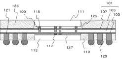
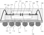
図1は、本実施形態に係る半導体装置の構成を模式的に示す断面図である。図1に示した半導体装置100は、平板状の配線体101と、配線体101の一方の面に設けられた第一の半導体素子113と、配線体101の第一の半導体素子113の設けられた側の面および第一の半導体素子113の側面を被覆する絶縁樹脂119と、配線体101の他方の面に、第二の半導体素子111に対向配置させて設けられた第二の半導体素子111と、を有する。
図1に示した半導体装置100において、配線体101は、絶縁膜107、シリコン層105および配線層103がこの順に積層された構造になっている。そして、配線層103中の導電体およびこれに接続して設けられた導体ヴィア109により構成される貫通電極が配線体101を貫通した構成となっている。また、配線体101の両面に第一の半導体素子113および第二の半導体素子111が対向して接合されている。
第一の実施形態に記載の半導体装置100(図1)は、配線層103、シリコン層105、絶縁膜107がこの順に積層された構成の配線体101を備えていたが、配線体101は、配線層103およびシリコン層105の積層体からなる構成としてもよい。図7は、本実施形態に係る半導体装置110の構成を模式的に示す断面図である。
以上の実施形態に記載の半導体装置において、配線体101が配線層103のみから構成されていてもよい。図8は、本実施形態に係る半導体装置120の構成を模式的に示す断面図である。
第一の実施形態に記載の半導体装置100において、配線体101の配線層103の側に接合された第一の半導体素子113が、複数の半導体素子の積層体であってもよい。図11は、本実施形態に係る半導体装置の構成を模式的に示す断面図である。図11に示した半導体装置の基本構成は第一の実施形態に記載の半導体装置100(図1)と同様であるが、第一の半導体素子113に代えて複数の半導体素子149が面の法線に沿って積層された構成である点が異なる。
以上の実施形態に記載の半導体装置において、配線体101の一つの面に複数の半導体素子が平面配置されていてもよい。以下、第四の実施形態に記載の半導体装置(図11)の場合を例に説明する。図13は、本実施形態に係る半導体装置の構成を模式的に示す断面図である。
以上の実施形態に記載の半導体装置において、配線体101中に設けられている導体ヴィア109を導体ワイヤとの接続部材として利用することもできる。また、配線体101の絶縁樹脂119形成面と対向する面に接着材により積層された複数の半導体素子が接続され、そのうち少なくとも1つの半導体素子が、ワイヤを介して、配線体101に電気的に接続された構成とすることができる。図14は、本実施形態に係る半導体装置の構成を模式的に示す断面図である。
図15(a)および図15(b)は、本実施形態に係る半導体装置の構成を模式的に示す断面図である。図15(a)は、図15(b)に示した半導体装置のボンディング前の状態を示す図である。図15(a)に示した半導体装置は、第三の実施形態に記載の配線層103からなる配線体101の一方の面に第一の半導体素子113が接合され、他方の面に第二の半導体素子111が配設された構成を有する。第一の半導体素子113は、配線体101上を覆う絶縁樹脂119中に埋設されている。なお、絶縁樹脂119を貫通する導体スルーホール121および導体スルーホール121に接続する電極端子123は、図15(a)においては設けられていない。
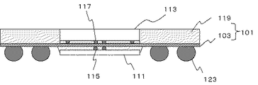
図17(a)および図17(b)は、本実施形態に係る半導体装置の構成を模式的に示す断面図である。図17(a)に示した半導体装置は、配線層103からなる平板状の配線体と、配線層103の一方の面に設けられた第一の半導体素子と、一方の面および第一の半導体素子の側面を被覆する絶縁樹脂119と、絶縁樹脂119を貫通する導体スルーホール121と、配線層103の他方の面に設けられた第二の半導体素子111と、を有する。
101 配線体
103 配線層
105 シリコン層
107 絶縁膜
109 導体ヴィア
110 半導体装置
111 半導体素子
113 半導体素子
115 電極
117 電極
119 絶縁樹脂
120 半導体装置
121 導体スルーホール
123 電極端子
125 アンダーフィル樹脂
127 アンダーフィル樹脂
129 基板
131 導体ポスト
133 シリコン基板
135 絶縁樹脂
137 シード層
139 接続電極
141 絶縁樹脂膜
143 開口部
145 ヴィアプラグ
147 配線
149 半導体素子
150 半導体装置
151 導体スルーホール
153 接着剤
155 ワイヤ
157 導体パッド
159 導体パッド
161 サポートリング
163 テープ基板
165 配線層
167 インナーリード封止樹脂
169 インナーリード
171 ヒートスプレッダ
173 配線基板
175 パッド
177 樹脂止めパターン
179 メモリ通信用電極
181 メモリ電極
183 外部入出力用電極
185 半導体装置
187 半導体装置
Claims (29)
- 平板状の配線体と、
前記配線体の一方の面に設けられた第一の半導体素子と、
前記一方の面の全面および前記第一の半導体素子の側面を被覆する封止樹脂と、
前記封止樹脂により被覆された後の前記配線体に接続され、前記配線体の他方の面に前記第一の半導体素子に対して少なくとも一部が対向する位置に設けられた第二の半導体素子と、を有し、
前記配線体は、
前記一方の面側に設けられ、前記第一の半導体素子と接続しており、前記配線体から露出した全面が前記封止樹脂によって被覆されている配線層と、
前記配線層の前記第一の半導体素子が接続されていない側に積層され、前記配線層を支持する支持層と、
前記支持層を貫通し、前記配線層と接続している貫通電極と、を備え、
前記配線体を介して前記第一の半導体素子と前記第二の半導体素子とが電気的に接続されており、
前記第二の半導体素子は前記他方の面に電極を介して接続されており、
前記貫通電極と前記電極とが前記配線体の面に対し、略垂直に一直線に接続され、
前記支持層がシリコン、セラミック、および珪ホウ酸ガラスからなる群から選択される一種以上の材料からなることを特徴とする半導体装置。 - 請求項1に記載の半導体装置において、
前記支持層はシリコンからなり、
前記配線体は前記他方の面側に絶縁膜をさらに備え、
前記貫通電極は前記支持層および前記絶縁膜を貫通して設けられていることを特徴とする半導体装置。 - 請求項1に記載の半導体装置において、
前記支持層はセラミックまたは珪ホウ酸ガラスからなることを特徴とする半導体装置。 - 請求項1乃至3いずれか1項に記載の半導体装置において、
前記貫通電極は、前記配線層を貫通することを特徴とする半導体装置。 - 請求項1乃至4いずれか1項に記載の半導体装置において、
平面視で前記第一の半導体素子と前記第二の半導体素子とが重なる部分において、前記第一の半導体素子と前記第二の半導体素子とが前記貫通電極を介して電気的に接続されていることを特徴とする半導体装置。 - 請求項1乃至5いずれか1項に記載の半導体装置において、
前記第一の半導体素子は、前記配線体の前記一方の面に第一の電極を介して接続され、
前記第二の半導体素子は、前記配線体の前記他方の面に第二の電極を介して接続されており、
前記第一の電極と前記貫通電極と前記第二の電極とが、前記配線層の面に対して略垂直に一直線に接続していることを特徴とする半導体装置。 - 請求項1乃至6いずれか1項に記載の半導体装置において、
前記第一の半導体素子は、前記配線体の前記一方の面に第一の電極を介して接続され、
前記第二の半導体素子は、前記配線体の前記他方の面に第二の電極を介して接続されており、
前記第一の電極及び前記第二の電極のすべてが、平面視で前記第一の半導体素子の内側の領域に配置されていることを特徴とする半導体装置。 - 請求項1乃至7いずれか1項に記載の半導体装置において、
前記貫通電極は、格子状に平面配置されていることを特徴とする半導体装置。 - 請求項8に記載の半導体装置において、
前記貫通電極は、正方格子状に平面配置されていることを特徴とする半導体装置。 - 請求項8に記載の半導体装置において、
前記貫通電極は、斜格子状に平面配置されていることを特徴とする半導体装置。 - 請求項1乃至10いずれか1項に記載の半導体装置において、
前記支持層は、能動素子が形成されたシリコン層であることを特徴とする半導体装置。 - 請求項1乃至11いずれか1項に記載の半導体装置において、
前記配線体は、絶縁膜と、前記支持層と、前記配線層とがこの順に積層された構成を有し、前記第一の半導体素子が前記配線層に接続され、前記第二の半導体素子が前記絶縁膜側に接続されていることを特徴とする半導体装置。 - 請求項1乃至12いずれか1項に記載の半導体装置において、
前記封止樹脂を貫通する貫通プラグを備えることを特徴とする半導体装置。 - 請求項1乃至13いずれか1項に記載の半導体装置において、
前記配線層が多層配線層であることを特徴とする半導体装置。 - 請求項1乃至14いずれか1項に記載の半導体装置において、
前記第一の半導体素子が前記封止樹脂に埋設されていることを特徴とする半導体装置。 - 請求項1乃至15いずれか1項に記載の半導体装置において、前記貫通電極は、前記配線体の前記他方の面に対し凸状に張り出していることを特徴とする半導体装置。
- 請求項1乃至16いずれか1項に記載の半導体装置において、前記貫通電極は、複数の導電体を積層して形成されていることを特徴とする半導体装置。
- 基板上に形成された支持層を貫通する導体ヴィアを形成する工程と、
前記基板上に前記導体ヴィアと接続し、前記支持層により支持される配線層を形成する工程と、
前記配線層と第一の半導体素子とを接続させる工程と、
前記配線層の前記配線体から露出した全面および前記第一の半導体素子の側面を封止樹脂により被覆する工程と、
前記基板の前記配線層の形成面の裏面から前記基板を薄化する工程と、
前記基板を薄化する前記工程の後に前記配線層を介して第二の半導体素子の少なくとも一部を前記第一の半導体素子に対向させ、前記導体ヴィアを介して前記第一の半導体素子と前記第二の半導体素子とを電気的に接続する工程と、
を含み、
前記配線層の表面および前記第一の半導体素子の側面を封止樹脂により被覆する前記工程は、前記基板上に形成された前記配線層の表面の全面を前記封止樹脂により覆う工程を含み、
前記第一の半導体素子と前記第二の半導体素子とを電気的に接続する前記工程において、前記支持層側の表面に露出させた前記導体ヴィアに電極を介して前記第二の半導体素子を接続し、前記導体ヴィアと前記電極とを前記配線層の面に対し、略垂直に一直線に接続させ、
前記支持層がシリコン、セラミック、および珪ホウ酸ガラスからなる群から選択される一種以上の材料からなることを特徴とする半導体装置の製造方法。 - 請求項18に記載の半導体装置の製造方法において、
導体ヴィアを形成する前記工程は、シリコンからなる前記支持層との間に絶縁層が形成された前記基板の前記絶縁層及び前記支持層に前記導体ヴィアを貫通させることを特徴とする半導体装置の製造方法。 - 請求項18に記載の半導体装置の製造方法において、
導体ヴィアを形成する前記工程は、セラミックまたは珪ホウ酸ガラスからなる前記支持層に前記導体ヴィアを貫通させることを特徴とする半導体装置の製造方法。 - 請求項18乃至20いずれか1項に記載の半導体装置の製造方法において、
前記第一の半導体素子と前記第二の半導体素子とを電気的に接続する前記工程は、平面視で前記第一の半導体素子と前記第二の半導体素子とが重なる部分において、前記導体ヴィアを介して前記第一の半導体素子と前記第二の半導体素子とを電気的に接続させる工程を含むことを特徴とする半導体装置の製造方法。 - 請求項18乃至21いずれか1項に記載の半導体装置の製造方法において、
前記第一の半導体素子と前記第二の半導体素子とを電気的に接続する前記工程は、前記第一の半導体素子を前記配線層の一方の面に第一の電極を介して接続し、前記第二の半導体素子を前記配線層の他方の面に第二の電極を介して接続し、前記第一の電極と前記導体ヴィアと前記第二の電極とを前記配線層の面に対して略垂直に一直線に接続させる工程を含むことを特徴とする半導体装置の製造方法。 - 請求項18乃至22いずれか1項に記載の半導体装置の製造方法において、
基板を薄化する前記工程は、前記基板を除去し、前記導体ヴィアの表面を露出させる工程を含むことを特徴とする半導体装置の製造方法。 - 請求項18乃至23いずれか1項に記載の半導体装置の製造方法において、
配線層を形成する前記工程は、
表面に絶縁膜と前記配線層を支持する支持層とがこの順に積層された前記基板を準備する工程と、
前記支持層上に前記配線層を設ける工程と、
を含むことを特徴とする半導体装置の製造方法。 - 請求項18乃至24いずれか1項に記載の半導体装置の製造方法において、
前記導体ヴィアは、格子状に平面配置されていることを特徴とする半導体装置の製造方法。 - 請求項25に記載の半導体装置の製造方法において、
前記導体ヴィアは、正方格子状に平面配置されていることを特徴とする半導体装置の製造方法。 - 請求項25に記載の半導体装置の製造方法において、
前記導体ヴィアは、斜格子状に平面配置されていることを特徴とする半導体装置の製造方法。 - 請求項18乃至27いずれか1項に記載の半導体装置の製造方法において、
前記基板がシリコン基板であることを特徴とする半導体装置の製造方法。 - 請求項18乃至28いずれか1項に記載の半導体装置の製造方法において、
前記配線層の表面および前記第一の半導体素子の側面を封止樹脂により被覆する前記工程は、
前記配線層の表面の全面を前記封止樹脂により封止することにより前記第一の半導体素子を埋設する工程と、
前記第一の半導体素子を埋設する前記工程の後に、前記封止樹脂を薄化して前記第一の半導体素子の表面を露出させる工程と、
を含むことを特徴とする半導体装置の製造方法。
Priority Applications (9)
| Application Number | Priority Date | Filing Date | Title |
|---|---|---|---|
| JP2004194690A JP4865197B2 (ja) | 2004-06-30 | 2004-06-30 | 半導体装置およびその製造方法 |
| US11/159,157 US7795721B2 (en) | 2004-06-30 | 2005-06-23 | Semiconductor device and method for manufacturing the same |
| US12/169,930 US8193033B2 (en) | 2004-06-30 | 2008-07-09 | Semiconductor device having a sealing resin and method of manufacturing the same |
| US12/850,232 US8207605B2 (en) | 2004-06-30 | 2010-08-04 | Semiconductor device having a sealing resin and method of manufacturing the same |
| US13/495,494 US8541874B2 (en) | 2004-06-30 | 2012-06-13 | Semiconductor device |
| US13/972,162 US8890305B2 (en) | 2004-06-30 | 2013-08-21 | Semiconductor device |
| US14/524,718 US9324699B2 (en) | 2004-06-30 | 2014-10-27 | Semiconductor device |
| US15/072,803 US20160204092A1 (en) | 2004-06-30 | 2016-03-17 | Semiconductor device |
| US16/375,282 US10672750B2 (en) | 2004-06-30 | 2019-04-04 | Semiconductor device |
Applications Claiming Priority (1)
| Application Number | Priority Date | Filing Date | Title |
|---|---|---|---|
| JP2004194690A JP4865197B2 (ja) | 2004-06-30 | 2004-06-30 | 半導体装置およびその製造方法 |
Related Child Applications (2)
| Application Number | Title | Priority Date | Filing Date |
|---|---|---|---|
| JP2009114222A Division JP5171726B2 (ja) | 2009-05-11 | 2009-05-11 | 半導体装置 |
| JP2009298355A Division JP5091221B2 (ja) | 2009-12-28 | 2009-12-28 | 半導体装置 |
Publications (3)
| Publication Number | Publication Date |
|---|---|
| JP2006019433A JP2006019433A (ja) | 2006-01-19 |
| JP2006019433A5 JP2006019433A5 (ja) | 2007-10-11 |
| JP4865197B2 true JP4865197B2 (ja) | 2012-02-01 |
Family
ID=35793426
Family Applications (1)
| Application Number | Title | Priority Date | Filing Date |
|---|---|---|---|
| JP2004194690A Active JP4865197B2 (ja) | 2004-06-30 | 2004-06-30 | 半導体装置およびその製造方法 |
Country Status (2)
| Country | Link |
|---|---|
| US (8) | US7795721B2 (ja) |
| JP (1) | JP4865197B2 (ja) |
Cited By (2)
| Publication number | Priority date | Publication date | Assignee | Title |
|---|---|---|---|---|
| KR20200031322A (ko) | 2018-09-14 | 2020-03-24 | 삼성전기주식회사 | 전자 소자 모듈 및 그 제조 방법 |
| US10991673B2 (en) | 2018-01-04 | 2021-04-27 | Kabushiki Kaisha Toshiba | Electronic device |
Families Citing this family (163)
| Publication number | Priority date | Publication date | Assignee | Title |
|---|---|---|---|---|
| JP4865197B2 (ja) | 2004-06-30 | 2012-02-01 | ルネサスエレクトロニクス株式会社 | 半導体装置およびその製造方法 |
| JP4880218B2 (ja) * | 2004-12-22 | 2012-02-22 | 三洋電機株式会社 | 回路装置 |
| JP2006216911A (ja) * | 2005-02-07 | 2006-08-17 | Renesas Technology Corp | 半導体装置およびカプセル型半導体パッケージ |
| JP4507101B2 (ja) * | 2005-06-30 | 2010-07-21 | エルピーダメモリ株式会社 | 半導体記憶装置及びその製造方法 |
| JP4787559B2 (ja) * | 2005-07-26 | 2011-10-05 | ルネサスエレクトロニクス株式会社 | 半導体装置およびその製造方法 |
| US20070252260A1 (en) * | 2006-04-28 | 2007-11-01 | Micron Technology, Inc. | Stacked die packages |
| JP2008016508A (ja) * | 2006-07-03 | 2008-01-24 | Nec Electronics Corp | 半導体装置およびその製造方法 |
| JP2008091638A (ja) | 2006-10-02 | 2008-04-17 | Nec Electronics Corp | 電子装置およびその製造方法 |
| EP1950806A1 (en) * | 2006-11-30 | 2008-07-30 | Matsushita Electric Industrial Co., Ltd. | Interposer with built-in passive part |
| JP4897451B2 (ja) * | 2006-12-04 | 2012-03-14 | ルネサスエレクトロニクス株式会社 | 半導体装置 |
| JP5183949B2 (ja) * | 2007-03-30 | 2013-04-17 | 日本電気株式会社 | 半導体装置の製造方法 |
| JP5125185B2 (ja) * | 2007-04-03 | 2013-01-23 | 株式会社ニコン | 半導体装置 |
| JP2008294423A (ja) | 2007-04-24 | 2008-12-04 | Nec Electronics Corp | 半導体装置 |
| KR100909322B1 (ko) * | 2007-07-02 | 2009-07-24 | 주식회사 네패스 | 초박형 반도체 패키지 및 그 제조방법 |
| JP5068133B2 (ja) * | 2007-10-17 | 2012-11-07 | 新光電気工業株式会社 | 半導体チップ積層構造体及び半導体装置 |
| KR20090056044A (ko) * | 2007-11-29 | 2009-06-03 | 삼성전자주식회사 | 반도체 소자 패키지 및 이를 제조하는 방법 |
| KR100925665B1 (ko) * | 2007-12-10 | 2009-11-06 | 주식회사 네패스 | 시스템 인 패키지 및 그 제조 방법 |
| US8456002B2 (en) | 2007-12-14 | 2013-06-04 | Stats Chippac Ltd. | Semiconductor device and method of forming insulating layer disposed over the semiconductor die for stress relief |
| US8183095B2 (en) | 2010-03-12 | 2012-05-22 | Stats Chippac, Ltd. | Semiconductor device and method of forming sacrificial protective layer to protect semiconductor die edge during singulation |
| US8343809B2 (en) | 2010-03-15 | 2013-01-01 | Stats Chippac, Ltd. | Semiconductor device and method of forming repassivation layer with reduced opening to contact pad of semiconductor die |
| US7767496B2 (en) | 2007-12-14 | 2010-08-03 | Stats Chippac, Ltd. | Semiconductor device and method of forming interconnect structure for encapsulated die having pre-applied protective layer |
| US9318441B2 (en) | 2007-12-14 | 2016-04-19 | Stats Chippac, Ltd. | Semiconductor device and method of forming sacrificial adhesive over contact pads of semiconductor die |
| US7867819B2 (en) | 2007-12-27 | 2011-01-11 | Sandisk Corporation | Semiconductor package including flip chip controller at bottom of die stack |
| WO2009084300A1 (ja) | 2007-12-28 | 2009-07-09 | Ibiden Co., Ltd. | インターポーザー及びインターポーザーの製造方法 |
| WO2009084299A1 (ja) | 2007-12-28 | 2009-07-09 | Ibiden Co., Ltd. | インターポーザー及びインターポーザーの製造方法 |
| US8273603B2 (en) * | 2008-04-04 | 2012-09-25 | The Charles Stark Draper Laboratory, Inc. | Interposers, electronic modules, and methods for forming the same |
| US8017451B2 (en) | 2008-04-04 | 2011-09-13 | The Charles Stark Draper Laboratory, Inc. | Electronic modules and methods for forming the same |
| JP2009295740A (ja) * | 2008-06-04 | 2009-12-17 | Elpida Memory Inc | メモリチップ及び半導体装置 |
| JP5078808B2 (ja) * | 2008-09-03 | 2012-11-21 | ラピスセミコンダクタ株式会社 | 半導体装置の製造方法 |
| US8063475B2 (en) * | 2008-09-26 | 2011-11-22 | Stats Chippac Ltd. | Semiconductor package system with through silicon via interposer |
| US8314499B2 (en) * | 2008-11-14 | 2012-11-20 | Fairchild Semiconductor Corporation | Flexible and stackable semiconductor die packages having thin patterned conductive layers |
| US8129824B1 (en) * | 2008-12-03 | 2012-03-06 | Amkor Technology, Inc. | Shielding for a semiconductor package |
| US7993941B2 (en) | 2008-12-05 | 2011-08-09 | Stats Chippac, Ltd. | Semiconductor package and method of forming Z-direction conductive posts embedded in structurally protective encapsulant |
| US8354304B2 (en) * | 2008-12-05 | 2013-01-15 | Stats Chippac, Ltd. | Semiconductor device and method of forming conductive posts embedded in photosensitive encapsulant |
| US8399983B1 (en) * | 2008-12-11 | 2013-03-19 | Xilinx, Inc. | Semiconductor assembly with integrated circuit and companion device |
| JP5058144B2 (ja) * | 2008-12-25 | 2012-10-24 | 新光電気工業株式会社 | 半導体素子の樹脂封止方法 |
| KR101004684B1 (ko) * | 2008-12-26 | 2011-01-04 | 주식회사 하이닉스반도체 | 적층형 반도체 패키지 |
| US9735136B2 (en) * | 2009-03-09 | 2017-08-15 | Micron Technology, Inc. | Method for embedding silicon die into a stacked package |
| JP2010245107A (ja) * | 2009-04-01 | 2010-10-28 | Shinko Electric Ind Co Ltd | 半導体装置及びその製造方法 |
| JP2010245383A (ja) * | 2009-04-08 | 2010-10-28 | Elpida Memory Inc | 半導体装置および半導体装置の製造方法 |
| US20100314730A1 (en) * | 2009-06-16 | 2010-12-16 | Broadcom Corporation | Stacked hybrid interposer through silicon via (TSV) package |
| US8227904B2 (en) * | 2009-06-24 | 2012-07-24 | Intel Corporation | Multi-chip package and method of providing die-to-die interconnects in same |
| US8378230B2 (en) | 2009-07-23 | 2013-02-19 | Ibiden Co., Ltd. | Printed wiring board and method for manufacturing the same |
| US8039304B2 (en) * | 2009-08-12 | 2011-10-18 | Stats Chippac, Ltd. | Semiconductor device and method of dual-molding die formed on opposite sides of build-up interconnect structures |
| US8410376B2 (en) | 2009-08-28 | 2013-04-02 | Ibiden Co., Ltd. | Printed wiring board and method for manufacturing the same |
| US20110050334A1 (en) * | 2009-09-02 | 2011-03-03 | Qualcomm Incorporated | Integrated Voltage Regulator with Embedded Passive Device(s) |
| JP5715334B2 (ja) | 2009-10-15 | 2015-05-07 | ルネサスエレクトロニクス株式会社 | 半導体装置 |
| US8008121B2 (en) * | 2009-11-04 | 2011-08-30 | Stats Chippac, Ltd. | Semiconductor package and method of mounting semiconductor die to opposite sides of TSV substrate |
| US9999129B2 (en) * | 2009-11-12 | 2018-06-12 | Intel Corporation | Microelectronic device and method of manufacturing same |
| FR2953064B1 (fr) | 2009-11-20 | 2011-12-16 | St Microelectronics Tours Sas | Procede d'encapsulation de composants electroniques sur tranche |
| EP2330618A1 (en) | 2009-12-04 | 2011-06-08 | STMicroelectronics (Grenoble 2) SAS | Rebuilt wafer assembly |
| US20110186960A1 (en) | 2010-02-03 | 2011-08-04 | Albert Wu | Techniques and configurations for recessed semiconductor substrates |
| US9385095B2 (en) | 2010-02-26 | 2016-07-05 | Taiwan Semiconductor Manufacturing Company, Ltd. | 3D semiconductor package interposer with die cavity |
| US8519537B2 (en) | 2010-02-26 | 2013-08-27 | Taiwan Semiconductor Manufacturing Company, Ltd. | 3D semiconductor package interposer with die cavity |
| US9548240B2 (en) | 2010-03-15 | 2017-01-17 | STATS ChipPAC Pte. Ltd. | Semiconductor device and method of forming repassivation layer for robust low cost fan-out semiconductor package |
| US8618654B2 (en) * | 2010-07-20 | 2013-12-31 | Marvell World Trade Ltd. | Structures embedded within core material and methods of manufacturing thereof |
| US8742603B2 (en) * | 2010-05-20 | 2014-06-03 | Qualcomm Incorporated | Process for improving package warpage and connection reliability through use of a backside mold configuration (BSMC) |
| US9735113B2 (en) | 2010-05-24 | 2017-08-15 | STATS ChipPAC Pte. Ltd. | Semiconductor device and method of forming ultra thin multi-die face-to-face WLCSP |
| US10159154B2 (en) * | 2010-06-03 | 2018-12-18 | Hsio Technologies, Llc | Fusion bonded liquid crystal polymer circuit structure |
| KR101710178B1 (ko) * | 2010-06-29 | 2017-02-24 | 삼성전자 주식회사 | 임베디이드 칩 온 칩 패키지 및 이를 포함하는 패키지 온 패키지 |
| US9048112B2 (en) | 2010-06-29 | 2015-06-02 | Qualcomm Incorporated | Integrated voltage regulator with embedded passive device(s) for a stacked IC |
| KR101123805B1 (ko) * | 2010-07-26 | 2012-03-12 | 주식회사 하이닉스반도체 | 스택 패키지 및 그 제조방법 |
| US8435835B2 (en) * | 2010-09-02 | 2013-05-07 | Stats Chippac, Ltd. | Semiconductor device and method of forming base leads from base substrate as standoff for stacking semiconductor die |
| KR101207273B1 (ko) * | 2010-09-03 | 2012-12-03 | 에스케이하이닉스 주식회사 | 임베디드 패키지 및 그 형성방법 |
| JP2012114173A (ja) * | 2010-11-23 | 2012-06-14 | Shinko Electric Ind Co Ltd | 半導体装置の製造方法及び半導体装置 |
| US8619431B2 (en) * | 2010-12-22 | 2013-12-31 | ADL Engineering Inc. | Three-dimensional system-in-package package-on-package structure |
| JP2012169440A (ja) * | 2011-02-14 | 2012-09-06 | Fujitsu Semiconductor Ltd | 半導体装置及びその製造方法 |
| US8841765B2 (en) * | 2011-04-22 | 2014-09-23 | Tessera, Inc. | Multi-chip module with stacked face-down connected dies |
| US8642382B2 (en) * | 2011-06-20 | 2014-02-04 | Stats Chippac Ltd. | Integrated circuit packaging system with support structure and method of manufacture thereof |
| US8823165B2 (en) | 2011-07-12 | 2014-09-02 | Invensas Corporation | Memory module in a package |
| US8502390B2 (en) | 2011-07-12 | 2013-08-06 | Tessera, Inc. | De-skewed multi-die packages |
| US8513817B2 (en) | 2011-07-12 | 2013-08-20 | Invensas Corporation | Memory module in a package |
| US8552567B2 (en) | 2011-07-27 | 2013-10-08 | Micron Technology, Inc. | Semiconductor die assemblies, semiconductor devices including same, and methods of fabrication |
| US8937309B2 (en) * | 2011-08-08 | 2015-01-20 | Micron Technology, Inc. | Semiconductor die assemblies, semiconductor devices including same, and methods of fabrication |
| US8461676B2 (en) | 2011-09-09 | 2013-06-11 | Qualcomm Incorporated | Soldering relief method and semiconductor device employing same |
| JPWO2013035655A1 (ja) * | 2011-09-09 | 2015-03-23 | 株式会社村田製作所 | モジュール基板 |
| US20130075923A1 (en) * | 2011-09-23 | 2013-03-28 | YeongIm Park | Integrated circuit packaging system with encapsulation and method of manufacture thereof |
| US8659142B2 (en) | 2011-10-03 | 2014-02-25 | Invensas Corporation | Stub minimization for wirebond assemblies without windows |
| US8436457B2 (en) | 2011-10-03 | 2013-05-07 | Invensas Corporation | Stub minimization for multi-die wirebond assemblies with parallel windows |
| US8610260B2 (en) | 2011-10-03 | 2013-12-17 | Invensas Corporation | Stub minimization for assemblies without wirebonds to package substrate |
| US8441111B2 (en) | 2011-10-03 | 2013-05-14 | Invensas Corporation | Stub minimization for multi-die wirebond assemblies with parallel windows |
| US8436477B2 (en) | 2011-10-03 | 2013-05-07 | Invensas Corporation | Stub minimization using duplicate sets of signal terminals in assemblies without wirebonds to package substrate |
| EP2764543A2 (en) | 2011-10-03 | 2014-08-13 | Invensas Corporation | Stub minimization for multi-die wirebond assemblies with parallel windows |
| KR20140069343A (ko) | 2011-10-03 | 2014-06-09 | 인벤사스 코포레이션 | 패키지의 중심으로부터 옵셋된 단자 그리드를 구비하는 스터드 최소화 |
| EP2769409A1 (en) | 2011-10-03 | 2014-08-27 | Invensas Corporation | Stub minimization for multi-die wirebond assemblies with orthogonal windows |
| US8653646B2 (en) | 2011-10-03 | 2014-02-18 | Invensas Corporation | Stub minimization using duplicate sets of terminals for wirebond assemblies without windows |
| JP2013110264A (ja) * | 2011-11-21 | 2013-06-06 | Fujitsu Semiconductor Ltd | 半導体装置及び半導体装置の製造方法 |
| WO2013084384A1 (ja) * | 2011-12-08 | 2013-06-13 | パナソニック株式会社 | 半導体装置及びその製造方法 |
| US8860222B2 (en) | 2011-12-27 | 2014-10-14 | Maxim Integrated Products, Inc. | Techniques for wafer-level processing of QFN packages |
| EP2613349B1 (en) * | 2012-01-05 | 2019-11-20 | Nxp B.V. | Semiconductor package with improved thermal properties |
| US9691706B2 (en) | 2012-01-23 | 2017-06-27 | Taiwan Semiconductor Manufacturing Company, Ltd. | Multi-chip fan out package and methods of forming the same |
| JP2013197387A (ja) * | 2012-03-21 | 2013-09-30 | Elpida Memory Inc | 半導体装置 |
| US9006004B2 (en) * | 2012-03-23 | 2015-04-14 | Taiwan Semiconductor Manufacturing Company, Ltd. | Probing chips during package formation |
| US9613917B2 (en) | 2012-03-30 | 2017-04-04 | Taiwan Semiconductor Manufacturing Company, Ltd. | Package-on-package (PoP) device with integrated passive device in a via |
| WO2013153742A1 (ja) * | 2012-04-11 | 2013-10-17 | パナソニック株式会社 | 半導体装置 |
| US8901730B2 (en) | 2012-05-03 | 2014-12-02 | Taiwan Semiconductor Manufacturing Company, Ltd. | Methods and apparatus for package on package devices |
| TWI485826B (zh) * | 2012-05-25 | 2015-05-21 | Ind Tech Res Inst | 晶片堆疊結構以及晶片堆疊結構的製作方法 |
| JP5607692B2 (ja) * | 2012-08-22 | 2014-10-15 | ルネサスエレクトロニクス株式会社 | 電子装置 |
| US9368477B2 (en) | 2012-08-27 | 2016-06-14 | Invensas Corporation | Co-support circuit panel and microelectronic packages |
| US8848391B2 (en) | 2012-08-27 | 2014-09-30 | Invensas Corporation | Co-support component and microelectronic assembly |
| US8848392B2 (en) | 2012-08-27 | 2014-09-30 | Invensas Corporation | Co-support module and microelectronic assembly |
| US8787034B2 (en) | 2012-08-27 | 2014-07-22 | Invensas Corporation | Co-support system and microelectronic assembly |
| US9165887B2 (en) | 2012-09-10 | 2015-10-20 | Taiwan Semiconductor Manufacturing Company, Ltd. | Semiconductor device with discrete blocks |
| US9391041B2 (en) | 2012-10-19 | 2016-07-12 | Taiwan Semiconductor Manufacturing Company, Ltd. | Fan-out wafer level package structure |
| JP6290534B2 (ja) * | 2012-12-20 | 2018-03-07 | 新光電気工業株式会社 | 半導体パッケージ及び半導体パッケージの製造方法 |
| US9087779B2 (en) * | 2013-01-02 | 2015-07-21 | Maxim Integrated Products, Inc. | Multi-die, high current wafer level package |
| JP6409575B2 (ja) | 2013-01-30 | 2018-10-24 | パナソニック株式会社 | 積層型半導体装置 |
| US8970023B2 (en) | 2013-02-04 | 2015-03-03 | Taiwan Semiconductor Manufacturing Company, Ltd. | Package structure and methods of forming same |
| US8993380B2 (en) | 2013-03-08 | 2015-03-31 | Taiwan Semiconductor Manufacturing Company, Ltd. | Structure and method for 3D IC package |
| USD707332S1 (en) | 2013-03-15 | 2014-06-17 | S.P.M. Flow Control, Inc. | Seal assembly |
| US20160079207A1 (en) * | 2013-04-23 | 2016-03-17 | PS4 Luxco S.a.r..L. | Semiconductor device and method for manufacturing same |
| CN103268875B (zh) * | 2013-05-30 | 2015-06-03 | 山东华芯微电子科技有限公司 | 一种多晶片封装结构 |
| US9070423B2 (en) | 2013-06-11 | 2015-06-30 | Invensas Corporation | Single package dual channel memory with co-support |
| US10667410B2 (en) | 2013-07-11 | 2020-05-26 | Hsio Technologies, Llc | Method of making a fusion bonded circuit structure |
| KR101548801B1 (ko) * | 2013-08-28 | 2015-08-31 | 삼성전기주식회사 | 전자 소자 모듈 및 그 제조 방법 |
| US9123555B2 (en) | 2013-10-25 | 2015-09-01 | Invensas Corporation | Co-support for XFD packaging |
| US9373527B2 (en) | 2013-10-30 | 2016-06-21 | Taiwan Semiconductor Manufacturing Company, Ltd. | Chip on package structure and method |
| US9184128B2 (en) | 2013-12-13 | 2015-11-10 | Taiwan Semiconductor Manufacturing Company, Ltd. | 3DIC package and methods of forming the same |
| US9653442B2 (en) * | 2014-01-17 | 2017-05-16 | Taiwan Semiconductor Manufacturing Company, Ltd. | Integrated circuit package and methods of forming same |
| US9653443B2 (en) | 2014-02-14 | 2017-05-16 | Taiwan Semiconductor Manufacturing Company, Ltd. | Thermal performance structure for semiconductor packages and method of forming same |
| US9935090B2 (en) * | 2014-02-14 | 2018-04-03 | Taiwan Semiconductor Manufacturing Company, Ltd. | Substrate design for semiconductor packages and method of forming same |
| US10026671B2 (en) * | 2014-02-14 | 2018-07-17 | Taiwan Semiconductor Manufacturing Company, Ltd. | Substrate design for semiconductor packages and method of forming same |
| US10056267B2 (en) * | 2014-02-14 | 2018-08-21 | Taiwan Semiconductor Manufacturing Company, Ltd. | Substrate design for semiconductor packages and method of forming same |
| US9768090B2 (en) | 2014-02-14 | 2017-09-19 | Taiwan Semiconductor Manufacturing Company, Ltd. | Substrate design for semiconductor packages and method of forming same |
| TWI616979B (zh) * | 2014-03-14 | 2018-03-01 | Toshiba Memory Corp | 半導體裝置及其製造方法 |
| JP6259737B2 (ja) | 2014-03-14 | 2018-01-10 | 東芝メモリ株式会社 | 半導体装置及びその製造方法 |
| JP2015195263A (ja) * | 2014-03-31 | 2015-11-05 | マイクロン テクノロジー, インク. | 半導体装置及びその製造方法 |
| TWI474417B (zh) * | 2014-06-16 | 2015-02-21 | Phoenix Pioneer Technology Co Ltd | 封裝方法 |
| KR20150144416A (ko) * | 2014-06-16 | 2015-12-28 | 한국전자통신연구원 | 적층 모듈 패키지 및 그 제조 방법 |
| US9281296B2 (en) | 2014-07-31 | 2016-03-08 | Invensas Corporation | Die stacking techniques in BGA memory package for small footprint CPU and memory motherboard design |
| US9691437B2 (en) | 2014-09-25 | 2017-06-27 | Invensas Corporation | Compact microelectronic assembly having reduced spacing between controller and memory packages |
| KR20160088233A (ko) * | 2014-12-19 | 2016-07-25 | 인텔 아이피 코포레이션 | 개선된 인터커넥트 대역폭을 갖는 적층된 반도체 디바이스 패키지 |
| KR102309463B1 (ko) * | 2015-01-23 | 2021-10-07 | 엘지이노텍 주식회사 | 시스템 인 패키지 모듈 |
| KR101672622B1 (ko) | 2015-02-09 | 2016-11-03 | 앰코 테크놀로지 코리아 주식회사 | 반도체 디바이스 및 그 제조 방법 |
| US9564416B2 (en) | 2015-02-13 | 2017-02-07 | Taiwan Semiconductor Manufacturing Company, Ltd. | Package structures and methods of forming the same |
| KR101684787B1 (ko) * | 2015-02-13 | 2016-12-08 | 타이완 세미콘덕터 매뉴팩쳐링 컴퍼니 리미티드 | 반도체 패키지 디바이스 및 그 형성 방법 |
| US9711488B2 (en) * | 2015-03-13 | 2017-07-18 | Mediatek Inc. | Semiconductor package assembly |
| US9595482B2 (en) | 2015-03-16 | 2017-03-14 | Taiwan Semiconductor Manufacturing Company, Ltd. | Structure for die probing |
| US9484080B1 (en) | 2015-11-09 | 2016-11-01 | Invensas Corporation | High-bandwidth memory application with controlled impedance loading |
| DE102016203453A1 (de) * | 2016-03-02 | 2017-09-07 | Fraunhofer-Gesellschaft zur Förderung der angewandten Forschung e.V. | Verfahren zur Herstellung eines Halbleiterbauelements und Halbleiterbauelement |
| KR101787886B1 (ko) * | 2016-04-12 | 2017-10-19 | 앰코 테크놀로지 코리아 주식회사 | 반도체 패키지 및 이의 제조 방법 |
| US9679613B1 (en) | 2016-05-06 | 2017-06-13 | Invensas Corporation | TFD I/O partition for high-speed, high-density applications |
| US10483237B2 (en) * | 2016-11-11 | 2019-11-19 | Semiconductor Components Industries, Llc | Vertically stacked multichip modules |
| CN106816421B (zh) * | 2017-03-22 | 2019-11-15 | 中芯长电半导体(江阴)有限公司 | 集成有功率传输芯片的封装结构的封装方法 |
| US10304800B2 (en) * | 2017-06-23 | 2019-05-28 | Taiwan Semiconductor Manufacturing Company Ltd. | Packaging with substrates connected by conductive bumps |
| US10957672B2 (en) * | 2017-11-13 | 2021-03-23 | Taiwan Semiconductor Manufacturing Company, Ltd. | Package structure and method of manufacturing the same |
| JP2018050077A (ja) * | 2017-12-14 | 2018-03-29 | ルネサスエレクトロニクス株式会社 | 電子装置 |
| JP2019110201A (ja) | 2017-12-18 | 2019-07-04 | ルネサスエレクトロニクス株式会社 | 電子装置および電子機器 |
| CN111788675B (zh) | 2018-03-20 | 2023-11-07 | 株式会社村田制作所 | 高频模块 |
| JP2018137474A (ja) * | 2018-04-16 | 2018-08-30 | ルネサスエレクトロニクス株式会社 | 電子装置 |
| US11276676B2 (en) * | 2018-05-15 | 2022-03-15 | Invensas Bonding Technologies, Inc. | Stacked devices and methods of fabrication |
| CN113016064A (zh) * | 2018-11-12 | 2021-06-22 | 株式会社村田制作所 | 安装型电子部件以及电子电路模块 |
| JP7163224B2 (ja) * | 2019-03-15 | 2022-10-31 | ルネサスエレクトロニクス株式会社 | 電子装置 |
| US10985151B2 (en) * | 2019-04-19 | 2021-04-20 | Nanya Technology Corporation | Semiconductor package and method for preparing the same |
| US11387177B2 (en) * | 2019-06-17 | 2022-07-12 | Taiwan Semiconductor Manufacturing Company Ltd. | Package structure and method for forming the same |
| US11362010B2 (en) * | 2019-10-16 | 2022-06-14 | Taiwan Semiconductor Manufacturing Co., Ltd. | Structure and formation method of chip package with fan-out feature |
| US11587918B2 (en) | 2019-12-17 | 2023-02-21 | Micron Technology, Inc. | Semiconductor devices, semiconductor device packages, electronic systems including same, and related methods |
| KR20210155455A (ko) * | 2020-06-16 | 2021-12-23 | 삼성전자주식회사 | 반도체 패키지 |
| JP6985477B1 (ja) * | 2020-09-25 | 2021-12-22 | アオイ電子株式会社 | 半導体装置および半導体装置の製造方法 |
| CN112908869A (zh) * | 2021-01-19 | 2021-06-04 | 上海先方半导体有限公司 | 一种封装结构及其制备方法 |
| US20230012350A1 (en) * | 2021-07-08 | 2023-01-12 | Taiwan Semiconductor Manufacturing Company, Ltd. | Semiconductor device package having warpage control and method of forming the same |
| FR3132977A1 (fr) * | 2022-02-22 | 2023-08-25 | Stmicroelectronics (Grenoble 2) Sas | Dispositif électronique |
| CN115101519A (zh) * | 2022-08-29 | 2022-09-23 | 盛合晶微半导体(江阴)有限公司 | 一种三维堆叠的扇出型封装结构及其制备方法 |
Family Cites Families (67)
| Publication number | Priority date | Publication date | Assignee | Title |
|---|---|---|---|---|
| JP2734684B2 (ja) * | 1989-10-03 | 1998-04-02 | 松下電器産業株式会社 | 半導体素子パッケージ |
| JPH04370958A (ja) * | 1991-06-20 | 1992-12-24 | Hitachi Ltd | 半導体基板、これを用いた半導体集積回路装置および半導体基板の製造方法 |
| JPH0548001A (ja) * | 1991-08-19 | 1993-02-26 | Fujitsu Ltd | 半導体集積回路の実装方法 |
| JPH07176684A (ja) | 1993-12-17 | 1995-07-14 | Interu Japan Kk | 半導体装置 |
| US5751015A (en) * | 1995-11-17 | 1998-05-12 | Micron Technology, Inc. | Semiconductor reliability test chip |
| EP0821407A3 (en) * | 1996-02-23 | 1998-03-04 | Matsushita Electric Industrial Co., Ltd. | Semiconductor devices having protruding contacts and method for making the same |
| JP3380151B2 (ja) | 1997-12-22 | 2003-02-24 | 新光電気工業株式会社 | 多層回路基板 |
| US6137164A (en) * | 1998-03-16 | 2000-10-24 | Texas Instruments Incorporated | Thin stacked integrated circuit device |
| JP3648053B2 (ja) * | 1998-04-30 | 2005-05-18 | 沖電気工業株式会社 | 半導体装置 |
| GB2338827B (en) * | 1998-06-27 | 2002-12-31 | Motorola Gmbh | Electronic package assembly |
| JP3563604B2 (ja) * | 1998-07-29 | 2004-09-08 | 株式会社東芝 | マルチチップ半導体装置及びメモリカード |
| US6281042B1 (en) * | 1998-08-31 | 2001-08-28 | Micron Technology, Inc. | Structure and method for a high performance electronic packaging assembly |
| US6424034B1 (en) | 1998-08-31 | 2002-07-23 | Micron Technology, Inc. | High performance packaging for microprocessors and DRAM chips which minimizes timing skews |
| JP3856967B2 (ja) | 1998-10-28 | 2006-12-13 | アルゼ株式会社 | 遊技機 |
| US6175160B1 (en) * | 1999-01-08 | 2001-01-16 | Intel Corporation | Flip-chip having an on-chip cache memory |
| US6274937B1 (en) * | 1999-02-01 | 2001-08-14 | Micron Technology, Inc. | Silicon multi-chip module packaging with integrated passive components and method of making |
| US7349223B2 (en) * | 2000-05-23 | 2008-03-25 | Nanonexus, Inc. | Enhanced compliant probe card systems having improved planarity |
| US6617681B1 (en) * | 1999-06-28 | 2003-09-09 | Intel Corporation | Interposer and method of making same |
| JP2001077301A (ja) * | 1999-08-24 | 2001-03-23 | Amkor Technology Korea Inc | 半導体パッケージ及びその製造方法 |
| US6255899B1 (en) * | 1999-09-01 | 2001-07-03 | International Business Machines Corporation | Method and apparatus for increasing interchip communications rates |
| JP3633559B2 (ja) * | 1999-10-01 | 2005-03-30 | セイコーエプソン株式会社 | 半導体装置及びその製造方法、回路基板並びに電子機器 |
| JP2001203318A (ja) * | 1999-12-17 | 2001-07-27 | Texas Instr Inc <Ti> | 複数のフリップチップを備えた半導体アセンブリ |
| JP2001177049A (ja) * | 1999-12-20 | 2001-06-29 | Toshiba Corp | 半導体装置及びicカード |
| GB0005088D0 (en) * | 2000-03-01 | 2000-04-26 | Unilever Plc | Composition and method for bleaching laundry fabrics |
| JP3597754B2 (ja) * | 2000-04-24 | 2004-12-08 | Necエレクトロニクス株式会社 | 半導体装置及びその製造方法 |
| JP2001345418A (ja) | 2000-06-02 | 2001-12-14 | Matsushita Electric Ind Co Ltd | 両面実装構造体の製造方法及びその両面実装構造体 |
| JP4701506B2 (ja) | 2000-09-14 | 2011-06-15 | ソニー株式会社 | 回路ブロック体の製造方法、配線回路装置の製造方法並びに半導体装置の製造方法 |
| JP2002176137A (ja) * | 2000-09-28 | 2002-06-21 | Toshiba Corp | 積層型半導体デバイス |
| US20020074637A1 (en) * | 2000-12-19 | 2002-06-20 | Intel Corporation | Stacked flip chip assemblies |
| JP2002221801A (ja) * | 2001-01-29 | 2002-08-09 | Hitachi Ltd | 配線基板の製造方法 |
| US6673653B2 (en) * | 2001-02-23 | 2004-01-06 | Eaglestone Partners I, Llc | Wafer-interposer using a ceramic substrate |
| US20020121707A1 (en) * | 2001-02-27 | 2002-09-05 | Chippac, Inc. | Super-thin high speed flip chip package |
| JP2002314031A (ja) | 2001-04-13 | 2002-10-25 | Fujitsu Ltd | マルチチップモジュール |
| SG106054A1 (en) * | 2001-04-17 | 2004-09-30 | Micron Technology Inc | Method and apparatus for package reduction in stacked chip and board assemblies |
| JP4831885B2 (ja) * | 2001-04-27 | 2011-12-07 | 株式会社半導体エネルギー研究所 | 半導体装置の作製方法 |
| JP2002343904A (ja) * | 2001-05-21 | 2002-11-29 | Matsushita Electric Ind Co Ltd | 半導体装置 |
| US7189595B2 (en) * | 2001-05-31 | 2007-03-13 | International Business Machines Corporation | Method of manufacture of silicon based package and devices manufactured thereby |
| JP4746770B2 (ja) * | 2001-06-19 | 2011-08-10 | ルネサスエレクトロニクス株式会社 | 半導体装置 |
| JP2003007910A (ja) * | 2001-06-19 | 2003-01-10 | Matsushita Electric Ind Co Ltd | 半導体装置 |
| JP4122143B2 (ja) * | 2001-07-26 | 2008-07-23 | 太陽誘電株式会社 | 半導体装置及びその製造方法 |
| US7176506B2 (en) * | 2001-08-28 | 2007-02-13 | Tessera, Inc. | High frequency chip packages with connecting elements |
| US6787916B2 (en) * | 2001-09-13 | 2004-09-07 | Tru-Si Technologies, Inc. | Structures having a substrate with a cavity and having an integrated circuit bonded to a contact pad located in the cavity |
| JP3959264B2 (ja) * | 2001-09-29 | 2007-08-15 | 株式会社東芝 | 積層型半導体装置 |
| JP3861669B2 (ja) * | 2001-11-22 | 2006-12-20 | ソニー株式会社 | マルチチップ回路モジュールの製造方法 |
| JP4044769B2 (ja) * | 2002-02-22 | 2008-02-06 | 富士通株式会社 | 半導体装置用基板及びその製造方法及び半導体パッケージ |
| JP2003273317A (ja) * | 2002-03-19 | 2003-09-26 | Nec Electronics Corp | 半導体装置及びその製造方法 |
| JP2003318361A (ja) * | 2002-04-19 | 2003-11-07 | Fujitsu Ltd | 半導体装置及びその製造方法 |
| JP2004039867A (ja) | 2002-07-03 | 2004-02-05 | Sony Corp | 多層配線回路モジュール及びその製造方法 |
| US7087988B2 (en) * | 2002-07-30 | 2006-08-08 | Kabushiki Kaisha Toshiba | Semiconductor packaging apparatus |
| JP2004079756A (ja) | 2002-08-16 | 2004-03-11 | Fujitsu Ltd | 薄膜多層配線基板、電子部品パッケージ、及び、電子部品パッケージの製造方法 |
| US20040046248A1 (en) * | 2002-09-05 | 2004-03-11 | Corning Intellisense Corporation | Microsystem packaging and associated methods |
| TWI322448B (en) * | 2002-10-08 | 2010-03-21 | Chippac Inc | Semiconductor stacked multi-package module having inverted second package |
| US7061122B2 (en) * | 2002-10-11 | 2006-06-13 | Tessera, Inc. | Components, methods and assemblies for multi-chip packages |
| JP3908146B2 (ja) * | 2002-10-28 | 2007-04-25 | シャープ株式会社 | 半導体装置及び積層型半導体装置 |
| JP3910907B2 (ja) | 2002-10-29 | 2007-04-25 | 新光電気工業株式会社 | キャパシタ素子及びこの製造方法、半導体装置用基板、並びに半導体装置 |
| US6798057B2 (en) * | 2002-11-05 | 2004-09-28 | Micron Technology, Inc. | Thin stacked ball-grid array package |
| JPWO2004047167A1 (ja) * | 2002-11-21 | 2006-03-23 | 日本電気株式会社 | 半導体装置、配線基板および配線基板製造方法 |
| US20040155358A1 (en) * | 2003-02-07 | 2004-08-12 | Toshitsune Iijima | First and second level packaging assemblies and method of assembling package |
| JP3917946B2 (ja) * | 2003-03-11 | 2007-05-23 | 富士通株式会社 | 積層型半導体装置 |
| JP2004288815A (ja) * | 2003-03-20 | 2004-10-14 | Seiko Epson Corp | 半導体装置及びその製造方法 |
| JP2004296963A (ja) * | 2003-03-28 | 2004-10-21 | Semiconductor Energy Lab Co Ltd | 半導体装置及び半導体装置の作製方法 |
| JP4419049B2 (ja) * | 2003-04-21 | 2010-02-24 | エルピーダメモリ株式会社 | メモリモジュール及びメモリシステム |
| JPWO2004102653A1 (ja) * | 2003-05-15 | 2006-07-13 | 新光電気工業株式会社 | 半導体装置およびインターポーザー |
| TWI245381B (en) * | 2003-08-14 | 2005-12-11 | Via Tech Inc | Electrical package and process thereof |
| US6864165B1 (en) * | 2003-09-15 | 2005-03-08 | International Business Machines Corporation | Method of fabricating integrated electronic chip with an interconnect device |
| US7049170B2 (en) * | 2003-12-17 | 2006-05-23 | Tru-Si Technologies, Inc. | Integrated circuits and packaging substrates with cavities, and attachment methods including insertion of protruding contact pads into cavities |
| JP4865197B2 (ja) * | 2004-06-30 | 2012-02-01 | ルネサスエレクトロニクス株式会社 | 半導体装置およびその製造方法 |
-
2004
- 2004-06-30 JP JP2004194690A patent/JP4865197B2/ja active Active
-
2005
- 2005-06-23 US US11/159,157 patent/US7795721B2/en active Active
-
2008
- 2008-07-09 US US12/169,930 patent/US8193033B2/en not_active Expired - Fee Related
-
2010
- 2010-08-04 US US12/850,232 patent/US8207605B2/en not_active Expired - Fee Related
-
2012
- 2012-06-13 US US13/495,494 patent/US8541874B2/en active Active
-
2013
- 2013-08-21 US US13/972,162 patent/US8890305B2/en active Active
-
2014
- 2014-10-27 US US14/524,718 patent/US9324699B2/en active Active
-
2016
- 2016-03-17 US US15/072,803 patent/US20160204092A1/en not_active Abandoned
-
2019
- 2019-04-04 US US16/375,282 patent/US10672750B2/en active Active
Cited By (5)
| Publication number | Priority date | Publication date | Assignee | Title |
|---|---|---|---|---|
| US10991673B2 (en) | 2018-01-04 | 2021-04-27 | Kabushiki Kaisha Toshiba | Electronic device |
| US11791311B2 (en) | 2018-01-04 | 2023-10-17 | Nagase & Co., Ltd. | Electronic device |
| KR20200031322A (ko) | 2018-09-14 | 2020-03-24 | 삼성전기주식회사 | 전자 소자 모듈 및 그 제조 방법 |
| US10820456B2 (en) | 2018-09-14 | 2020-10-27 | Samsung EIectro-Mechanics Co., Ltd. | Electronic component module and manufacturing method thereof |
| US11337346B2 (en) | 2018-09-14 | 2022-05-17 | Samsung Electro-Mechanics Co., Ltd. | Electronic component module and manufacturing method thereof |
Also Published As
| Publication number | Publication date |
|---|---|
| US20060063312A1 (en) | 2006-03-23 |
| US8541874B2 (en) | 2013-09-24 |
| US9324699B2 (en) | 2016-04-26 |
| US8193033B2 (en) | 2012-06-05 |
| US20160204092A1 (en) | 2016-07-14 |
| US20100314749A1 (en) | 2010-12-16 |
| US8207605B2 (en) | 2012-06-26 |
| US20130334705A1 (en) | 2013-12-19 |
| US7795721B2 (en) | 2010-09-14 |
| JP2006019433A (ja) | 2006-01-19 |
| US8890305B2 (en) | 2014-11-18 |
| US20190229104A1 (en) | 2019-07-25 |
| US20080265434A1 (en) | 2008-10-30 |
| US20120248620A1 (en) | 2012-10-04 |
| US10672750B2 (en) | 2020-06-02 |
| US20150041978A1 (en) | 2015-02-12 |
Similar Documents
| Publication | Publication Date | Title |
|---|---|---|
| JP4865197B2 (ja) | 半導体装置およびその製造方法 | |
| JP5091221B2 (ja) | 半導体装置 | |
| TWI544599B (zh) | 封裝結構之製法 | |
| KR20080038035A (ko) | 반도체 패키지 및 적층형 반도체 패키지 | |
| TW202038348A (zh) | 天線整合式封裝結構及其製造方法 | |
| US8692386B2 (en) | Semiconductor device, method of manufacturing semiconductor device, and electronic device | |
| JPS60160645A (ja) | 積層半導体集積回路装置 | |
| TWI581387B (zh) | 封裝結構及其製法 | |
| TWI550737B (zh) | 晶片封裝體及其製造方法 | |
| JP5358089B2 (ja) | 半導体装置 | |
| TWI574333B (zh) | 電子封裝件及其製法 | |
| JP5171726B2 (ja) | 半導体装置 | |
| KR101341619B1 (ko) | 반도체 패키지 및 그의 제조 방법 | |
| JP2007142026A (ja) | インターポーザとその製造方法及び半導体装置 | |
| JP4028211B2 (ja) | 半導体装置 | |
| JP3893268B2 (ja) | 半導体装置の製造方法 | |
| JPH09270490A (ja) | 接続部構造および接続方法並びに半導体装置およびその製造方法 | |
| JP3757766B2 (ja) | 半導体装置及びその製造方法、並びに電子機器 | |
| TW200939442A (en) | Semiconductor chip having TSV (through silicon via) and stacked assembly including the chips | |
| TW202121613A (zh) | 晶片封裝結構及其製造方法 | |
| WO2021018014A1 (zh) | 一种基于tsv的多芯片的封装结构及其制备方法 | |
| JP4356196B2 (ja) | 半導体装置組立体 | |
| KR101068305B1 (ko) | 적층형 반도체 패키지 및 그 제조 방법 | |
| CN114975396A (zh) | 封装结构及其形成方法 |
Legal Events
| Date | Code | Title | Description |
|---|---|---|---|
| A621 | Written request for application examination |
Free format text: JAPANESE INTERMEDIATE CODE: A621 Effective date: 20070517 |
|
| A521 | Request for written amendment filed |
Free format text: JAPANESE INTERMEDIATE CODE: A523 Effective date: 20070824 |
|
| A977 | Report on retrieval |
Free format text: JAPANESE INTERMEDIATE CODE: A971007 Effective date: 20090306 |
|
| A131 | Notification of reasons for refusal |
Free format text: JAPANESE INTERMEDIATE CODE: A131 Effective date: 20090310 |
|
| A521 | Request for written amendment filed |
Free format text: JAPANESE INTERMEDIATE CODE: A523 Effective date: 20090511 |
|
| A131 | Notification of reasons for refusal |
Free format text: JAPANESE INTERMEDIATE CODE: A131 Effective date: 20091104 |
|
| A521 | Request for written amendment filed |
Free format text: JAPANESE INTERMEDIATE CODE: A523 Effective date: 20091228 |
|
| A131 | Notification of reasons for refusal |
Free format text: JAPANESE INTERMEDIATE CODE: A131 Effective date: 20100202 |
|
| A521 | Request for written amendment filed |
Free format text: JAPANESE INTERMEDIATE CODE: A523 Effective date: 20100405 |
|
| A02 | Decision of refusal |
Free format text: JAPANESE INTERMEDIATE CODE: A02 Effective date: 20100511 |
|
| A521 | Request for written amendment filed |
Free format text: JAPANESE INTERMEDIATE CODE: A523 Effective date: 20100805 |
|
| A911 | Transfer to examiner for re-examination before appeal (zenchi) |
Free format text: JAPANESE INTERMEDIATE CODE: A911 Effective date: 20100817 |
|
| A912 | Re-examination (zenchi) completed and case transferred to appeal board |
Free format text: JAPANESE INTERMEDIATE CODE: A912 Effective date: 20100917 |
|
| A521 | Request for written amendment filed |
Free format text: JAPANESE INTERMEDIATE CODE: A523 Effective date: 20110930 |
|
| A01 | Written decision to grant a patent or to grant a registration (utility model) |
Free format text: JAPANESE INTERMEDIATE CODE: A01 |
|
| A61 | First payment of annual fees (during grant procedure) |
Free format text: JAPANESE INTERMEDIATE CODE: A61 Effective date: 20111110 |
|
| FPAY | Renewal fee payment (event date is renewal date of database) |
Free format text: PAYMENT UNTIL: 20141118 Year of fee payment: 3 |
|
| R150 | Certificate of patent or registration of utility model |
Ref document number: 4865197 Country of ref document: JP Free format text: JAPANESE INTERMEDIATE CODE: R150 Free format text: JAPANESE INTERMEDIATE CODE: R150 |
|
| S531 | Written request for registration of change of domicile |
Free format text: JAPANESE INTERMEDIATE CODE: R313531 |
|
| R350 | Written notification of registration of transfer |
Free format text: JAPANESE INTERMEDIATE CODE: R350 |