JP5889552B2 - 液晶表示装置の駆動方法 - Google Patents
液晶表示装置の駆動方法 Download PDFInfo
- Publication number
- JP5889552B2 JP5889552B2 JP2011142652A JP2011142652A JP5889552B2 JP 5889552 B2 JP5889552 B2 JP 5889552B2 JP 2011142652 A JP2011142652 A JP 2011142652A JP 2011142652 A JP2011142652 A JP 2011142652A JP 5889552 B2 JP5889552 B2 JP 5889552B2
- Authority
- JP
- Japan
- Prior art keywords
- row
- liquid crystal
- layer
- image signal
- light
- Prior art date
- Legal status (The legal status is an assumption and is not a legal conclusion. Google has not performed a legal analysis and makes no representation as to the accuracy of the status listed.)
- Expired - Fee Related
Links
- 239000004973 liquid crystal related substance Substances 0.000 title claims description 174
- 238000000034 method Methods 0.000 title claims description 54
- 239000004065 semiconductor Substances 0.000 claims description 69
- 230000001747 exhibiting effect Effects 0.000 claims description 37
- 230000005540 biological transmission Effects 0.000 claims description 36
- 238000002834 transmittance Methods 0.000 claims description 36
- QVGXLLKOCUKJST-UHFFFAOYSA-N atomic oxygen Chemical compound [O] QVGXLLKOCUKJST-UHFFFAOYSA-N 0.000 claims description 34
- 229910052760 oxygen Inorganic materials 0.000 claims description 34
- 239000001301 oxygen Substances 0.000 claims description 34
- 238000012937 correction Methods 0.000 claims description 29
- 238000001514 detection method Methods 0.000 claims description 29
- 239000000203 mixture Substances 0.000 claims description 28
- 239000011159 matrix material Substances 0.000 claims description 15
- 230000001678 irradiating effect Effects 0.000 claims description 8
- 230000015572 biosynthetic process Effects 0.000 claims description 3
- 239000010410 layer Substances 0.000 description 340
- 239000000758 substrate Substances 0.000 description 119
- 229910044991 metal oxide Inorganic materials 0.000 description 45
- 150000004706 metal oxides Chemical class 0.000 description 45
- 239000010408 film Substances 0.000 description 34
- 229910007541 Zn O Inorganic materials 0.000 description 27
- 239000000463 material Substances 0.000 description 26
- 229910052751 metal Inorganic materials 0.000 description 24
- 239000002184 metal Substances 0.000 description 23
- 238000003079 width control Methods 0.000 description 22
- 239000003086 colorant Substances 0.000 description 18
- 239000003990 capacitor Substances 0.000 description 17
- 238000010586 diagram Methods 0.000 description 17
- 230000006870 function Effects 0.000 description 17
- 229910001195 gallium oxide Inorganic materials 0.000 description 17
- 229910052733 gallium Inorganic materials 0.000 description 16
- 238000000926 separation method Methods 0.000 description 16
- TWNQGVIAIRXVLR-UHFFFAOYSA-N oxo(oxoalumanyloxy)alumane Chemical compound O=[Al]O[Al]=O TWNQGVIAIRXVLR-UHFFFAOYSA-N 0.000 description 15
- 239000000853 adhesive Substances 0.000 description 14
- 230000001070 adhesive effect Effects 0.000 description 14
- 238000012546 transfer Methods 0.000 description 14
- ZOKXTWBITQBERF-UHFFFAOYSA-N Molybdenum Chemical compound [Mo] ZOKXTWBITQBERF-UHFFFAOYSA-N 0.000 description 13
- 238000009792 diffusion process Methods 0.000 description 13
- 238000004519 manufacturing process Methods 0.000 description 13
- 239000011733 molybdenum Substances 0.000 description 13
- WFKWXMTUELFFGS-UHFFFAOYSA-N tungsten Chemical compound [W] WFKWXMTUELFFGS-UHFFFAOYSA-N 0.000 description 13
- 229910052721 tungsten Inorganic materials 0.000 description 13
- 239000010937 tungsten Substances 0.000 description 13
- IJGRMHOSHXDMSA-UHFFFAOYSA-N Atomic nitrogen Chemical compound N#N IJGRMHOSHXDMSA-UHFFFAOYSA-N 0.000 description 12
- AJNVQOSZGJRYEI-UHFFFAOYSA-N digallium;oxygen(2-) Chemical compound [O-2].[O-2].[O-2].[Ga+3].[Ga+3] AJNVQOSZGJRYEI-UHFFFAOYSA-N 0.000 description 12
- 229910052750 molybdenum Inorganic materials 0.000 description 12
- 229920005989 resin Polymers 0.000 description 12
- 239000011347 resin Substances 0.000 description 12
- 229910052710 silicon Inorganic materials 0.000 description 12
- XUIMIQQOPSSXEZ-UHFFFAOYSA-N Silicon Chemical compound [Si] XUIMIQQOPSSXEZ-UHFFFAOYSA-N 0.000 description 11
- XLOMVQKBTHCTTD-UHFFFAOYSA-N Zinc monoxide Chemical compound [Zn]=O XLOMVQKBTHCTTD-UHFFFAOYSA-N 0.000 description 11
- 239000011521 glass Substances 0.000 description 11
- 239000010703 silicon Substances 0.000 description 11
- VYPSYNLAJGMNEJ-UHFFFAOYSA-N silicon dioxide Inorganic materials O=[Si]=O VYPSYNLAJGMNEJ-UHFFFAOYSA-N 0.000 description 11
- GYHNNYVSQQEPJS-UHFFFAOYSA-N Gallium Chemical compound [Ga] GYHNNYVSQQEPJS-UHFFFAOYSA-N 0.000 description 10
- 229910052581 Si3N4 Inorganic materials 0.000 description 10
- 230000008859 change Effects 0.000 description 10
- 239000001257 hydrogen Substances 0.000 description 10
- 229910052739 hydrogen Inorganic materials 0.000 description 10
- HQVNEWCFYHHQES-UHFFFAOYSA-N silicon nitride Chemical compound N12[Si]34N5[Si]62N3[Si]51N64 HQVNEWCFYHHQES-UHFFFAOYSA-N 0.000 description 10
- 229910052782 aluminium Inorganic materials 0.000 description 9
- 238000003491 array Methods 0.000 description 9
- 238000012545 processing Methods 0.000 description 9
- 101100392125 Caenorhabditis elegans gck-1 gene Proteins 0.000 description 8
- UFHFLCQGNIYNRP-UHFFFAOYSA-N Hydrogen Chemical compound [H][H] UFHFLCQGNIYNRP-UHFFFAOYSA-N 0.000 description 8
- 229910052814 silicon oxide Inorganic materials 0.000 description 8
- 230000004888 barrier function Effects 0.000 description 7
- 229920003023 plastic Polymers 0.000 description 7
- 239000004033 plastic Substances 0.000 description 7
- XAGFODPZIPBFFR-UHFFFAOYSA-N aluminium Chemical compound [Al] XAGFODPZIPBFFR-UHFFFAOYSA-N 0.000 description 6
- 229910052795 boron group element Inorganic materials 0.000 description 6
- 230000000694 effects Effects 0.000 description 6
- 239000011810 insulating material Substances 0.000 description 6
- 229910052757 nitrogen Inorganic materials 0.000 description 6
- 230000001681 protective effect Effects 0.000 description 6
- 239000010936 titanium Substances 0.000 description 6
- 239000012790 adhesive layer Substances 0.000 description 5
- 239000000956 alloy Substances 0.000 description 5
- RNQKDQAVIXDKAG-UHFFFAOYSA-N aluminum gallium Chemical compound [Al].[Ga] RNQKDQAVIXDKAG-UHFFFAOYSA-N 0.000 description 5
- 229910021417 amorphous silicon Inorganic materials 0.000 description 5
- 239000011651 chromium Substances 0.000 description 5
- 239000011241 protective layer Substances 0.000 description 5
- 239000000565 sealant Substances 0.000 description 5
- 239000011787 zinc oxide Substances 0.000 description 5
- 101100392126 Caenorhabditis elegans gck-3 gene Proteins 0.000 description 4
- 229910045601 alloy Inorganic materials 0.000 description 4
- 238000004891 communication Methods 0.000 description 4
- 239000000470 constituent Substances 0.000 description 4
- 239000010949 copper Substances 0.000 description 4
- 230000008878 coupling Effects 0.000 description 4
- 238000010168 coupling process Methods 0.000 description 4
- 238000005859 coupling reaction Methods 0.000 description 4
- 230000006866 deterioration Effects 0.000 description 4
- 238000005530 etching Methods 0.000 description 4
- 239000007789 gas Substances 0.000 description 4
- 238000010438 heat treatment Methods 0.000 description 4
- 229910052738 indium Inorganic materials 0.000 description 4
- 239000012212 insulator Substances 0.000 description 4
- 150000004767 nitrides Chemical class 0.000 description 4
- 229920000139 polyethylene terephthalate Polymers 0.000 description 4
- 239000005020 polyethylene terephthalate Substances 0.000 description 4
- 125000006850 spacer group Chemical group 0.000 description 4
- XLYOFNOQVPJJNP-UHFFFAOYSA-N water Substances O XLYOFNOQVPJJNP-UHFFFAOYSA-N 0.000 description 4
- 229910052725 zinc Inorganic materials 0.000 description 4
- 239000011701 zinc Substances 0.000 description 4
- VYZAMTAEIAYCRO-UHFFFAOYSA-N Chromium Chemical compound [Cr] VYZAMTAEIAYCRO-UHFFFAOYSA-N 0.000 description 3
- 229910019092 Mg-O Inorganic materials 0.000 description 3
- 229910019395 Mg—O Inorganic materials 0.000 description 3
- PXHVJJICTQNCMI-UHFFFAOYSA-N Nickel Chemical compound [Ni] PXHVJJICTQNCMI-UHFFFAOYSA-N 0.000 description 3
- KDLHZDBZIXYQEI-UHFFFAOYSA-N Palladium Chemical compound [Pd] KDLHZDBZIXYQEI-UHFFFAOYSA-N 0.000 description 3
- GWEVSGVZZGPLCZ-UHFFFAOYSA-N Titan oxide Chemical compound O=[Ti]=O GWEVSGVZZGPLCZ-UHFFFAOYSA-N 0.000 description 3
- RTAQQCXQSZGOHL-UHFFFAOYSA-N Titanium Chemical compound [Ti] RTAQQCXQSZGOHL-UHFFFAOYSA-N 0.000 description 3
- 239000000919 ceramic Substances 0.000 description 3
- 229910052804 chromium Inorganic materials 0.000 description 3
- 230000003247 decreasing effect Effects 0.000 description 3
- AMGQUBHHOARCQH-UHFFFAOYSA-N indium;oxotin Chemical compound [In].[Sn]=O AMGQUBHHOARCQH-UHFFFAOYSA-N 0.000 description 3
- 229910021424 microcrystalline silicon Inorganic materials 0.000 description 3
- 238000002156 mixing Methods 0.000 description 3
- 230000004048 modification Effects 0.000 description 3
- 238000012986 modification Methods 0.000 description 3
- 229910021421 monocrystalline silicon Inorganic materials 0.000 description 3
- BPUBBGLMJRNUCC-UHFFFAOYSA-N oxygen(2-);tantalum(5+) Chemical compound [O-2].[O-2].[O-2].[O-2].[O-2].[Ta+5].[Ta+5] BPUBBGLMJRNUCC-UHFFFAOYSA-N 0.000 description 3
- -1 polyethylene terephthalate Polymers 0.000 description 3
- 239000010453 quartz Substances 0.000 description 3
- 229910052715 tantalum Inorganic materials 0.000 description 3
- GUVRBAGPIYLISA-UHFFFAOYSA-N tantalum atom Chemical compound [Ta] GUVRBAGPIYLISA-UHFFFAOYSA-N 0.000 description 3
- 229910001936 tantalum oxide Inorganic materials 0.000 description 3
- 239000010409 thin film Substances 0.000 description 3
- 229910052719 titanium Inorganic materials 0.000 description 3
- 229920000178 Acrylic resin Polymers 0.000 description 2
- 239000004925 Acrylic resin Substances 0.000 description 2
- XKRFYHLGVUSROY-UHFFFAOYSA-N Argon Chemical compound [Ar] XKRFYHLGVUSROY-UHFFFAOYSA-N 0.000 description 2
- RYGMFSIKBFXOCR-UHFFFAOYSA-N Copper Chemical compound [Cu] RYGMFSIKBFXOCR-UHFFFAOYSA-N 0.000 description 2
- 229910052779 Neodymium Inorganic materials 0.000 description 2
- 239000004695 Polyether sulfone Substances 0.000 description 2
- 238000001237 Raman spectrum Methods 0.000 description 2
- 229910000577 Silicon-germanium Inorganic materials 0.000 description 2
- 229910006404 SnO 2 Inorganic materials 0.000 description 2
- NIXOWILDQLNWCW-UHFFFAOYSA-N acrylic acid group Chemical group C(C=C)(=O)O NIXOWILDQLNWCW-UHFFFAOYSA-N 0.000 description 2
- 230000004397 blinking Effects 0.000 description 2
- 230000001413 cellular effect Effects 0.000 description 2
- 150000001875 compounds Chemical class 0.000 description 2
- 229910052802 copper Inorganic materials 0.000 description 2
- PMHQVHHXPFUNSP-UHFFFAOYSA-M copper(1+);methylsulfanylmethane;bromide Chemical compound Br[Cu].CSC PMHQVHHXPFUNSP-UHFFFAOYSA-M 0.000 description 2
- 239000013078 crystal Substances 0.000 description 2
- 239000011152 fibreglass Substances 0.000 description 2
- 229910052736 halogen Inorganic materials 0.000 description 2
- 150000002431 hydrogen Chemical class 0.000 description 2
- 238000002347 injection Methods 0.000 description 2
- 239000007924 injection Substances 0.000 description 2
- 229910010272 inorganic material Inorganic materials 0.000 description 2
- 239000011147 inorganic material Substances 0.000 description 2
- 239000011229 interlayer Substances 0.000 description 2
- 239000007788 liquid Substances 0.000 description 2
- 229910052748 manganese Inorganic materials 0.000 description 2
- QEFYFXOXNSNQGX-UHFFFAOYSA-N neodymium atom Chemical compound [Nd] QEFYFXOXNSNQGX-UHFFFAOYSA-N 0.000 description 2
- 239000010955 niobium Substances 0.000 description 2
- 230000003647 oxidation Effects 0.000 description 2
- 238000007254 oxidation reaction Methods 0.000 description 2
- 229920005668 polycarbonate resin Polymers 0.000 description 2
- 239000004431 polycarbonate resin Substances 0.000 description 2
- 229920006267 polyester film Polymers 0.000 description 2
- 229920006393 polyether sulfone Polymers 0.000 description 2
- 239000011112 polyethylene naphthalate Substances 0.000 description 2
- 229920001721 polyimide Polymers 0.000 description 2
- 229920002620 polyvinyl fluoride Polymers 0.000 description 2
- 230000008569 process Effects 0.000 description 2
- 239000010948 rhodium Substances 0.000 description 2
- 229910052594 sapphire Inorganic materials 0.000 description 2
- 239000010980 sapphire Substances 0.000 description 2
- 229910052706 scandium Inorganic materials 0.000 description 2
- SIXSYDAISGFNSX-UHFFFAOYSA-N scandium atom Chemical compound [Sc] SIXSYDAISGFNSX-UHFFFAOYSA-N 0.000 description 2
- 239000002356 single layer Substances 0.000 description 2
- 239000000243 solution Substances 0.000 description 2
- 239000002699 waste material Substances 0.000 description 2
- YVTHLONGBIQYBO-UHFFFAOYSA-N zinc indium(3+) oxygen(2-) Chemical compound [O--].[Zn++].[In+3] YVTHLONGBIQYBO-UHFFFAOYSA-N 0.000 description 2
- VHUUQVKOLVNVRT-UHFFFAOYSA-N Ammonium hydroxide Chemical compound [NH4+].[OH-] VHUUQVKOLVNVRT-UHFFFAOYSA-N 0.000 description 1
- JBRZTFJDHDCESZ-UHFFFAOYSA-N AsGa Chemical compound [As]#[Ga] JBRZTFJDHDCESZ-UHFFFAOYSA-N 0.000 description 1
- 201000005569 Gout Diseases 0.000 description 1
- 206010021143 Hypoxia Diseases 0.000 description 1
- 229910001182 Mo alloy Inorganic materials 0.000 description 1
- 239000004677 Nylon Substances 0.000 description 1
- 229920012266 Poly(ether sulfone) PES Polymers 0.000 description 1
- 239000004962 Polyamide-imide Substances 0.000 description 1
- 239000004642 Polyimide Substances 0.000 description 1
- 239000004372 Polyvinyl alcohol Substances 0.000 description 1
- KJTLSVCANCCWHF-UHFFFAOYSA-N Ruthenium Chemical compound [Ru] KJTLSVCANCCWHF-UHFFFAOYSA-N 0.000 description 1
- 229910020923 Sn-O Inorganic materials 0.000 description 1
- 229910001080 W alloy Inorganic materials 0.000 description 1
- HCHKCACWOHOZIP-UHFFFAOYSA-N Zinc Chemical compound [Zn] HCHKCACWOHOZIP-UHFFFAOYSA-N 0.000 description 1
- LEVVHYCKPQWKOP-UHFFFAOYSA-N [Si].[Ge] Chemical compound [Si].[Ge] LEVVHYCKPQWKOP-UHFFFAOYSA-N 0.000 description 1
- 230000002411 adverse Effects 0.000 description 1
- 239000005407 aluminoborosilicate glass Substances 0.000 description 1
- 235000011114 ammonium hydroxide Nutrition 0.000 description 1
- 238000004458 analytical method Methods 0.000 description 1
- 229910052786 argon Inorganic materials 0.000 description 1
- 208000003464 asthenopia Diseases 0.000 description 1
- 125000004429 atom Chemical group 0.000 description 1
- 229910052788 barium Inorganic materials 0.000 description 1
- DSAJWYNOEDNPEQ-UHFFFAOYSA-N barium atom Chemical compound [Ba] DSAJWYNOEDNPEQ-UHFFFAOYSA-N 0.000 description 1
- 239000005388 borosilicate glass Substances 0.000 description 1
- 239000006229 carbon black Substances 0.000 description 1
- 229910052800 carbon group element Inorganic materials 0.000 description 1
- 239000011248 coating agent Substances 0.000 description 1
- 238000000576 coating method Methods 0.000 description 1
- 229910017052 cobalt Inorganic materials 0.000 description 1
- 239000010941 cobalt Substances 0.000 description 1
- GUTLYIVDDKVIGB-UHFFFAOYSA-N cobalt atom Chemical compound [Co] GUTLYIVDDKVIGB-UHFFFAOYSA-N 0.000 description 1
- 230000000295 complement effect Effects 0.000 description 1
- 239000004020 conductor Substances 0.000 description 1
- 239000000356 contaminant Substances 0.000 description 1
- 238000011109 contamination Methods 0.000 description 1
- 238000002425 crystallisation Methods 0.000 description 1
- 230000008025 crystallization Effects 0.000 description 1
- 150000001925 cycloalkenes Chemical class 0.000 description 1
- 230000007547 defect Effects 0.000 description 1
- 208000037265 diseases, disorders, signs and symptoms Diseases 0.000 description 1
- 238000001704 evaporation Methods 0.000 description 1
- 238000000605 extraction Methods 0.000 description 1
- 239000004744 fabric Substances 0.000 description 1
- 230000002349 favourable effect Effects 0.000 description 1
- 229910052732 germanium Inorganic materials 0.000 description 1
- GNPVGFCGXDBREM-UHFFFAOYSA-N germanium atom Chemical compound [Ge] GNPVGFCGXDBREM-UHFFFAOYSA-N 0.000 description 1
- 229910052735 hafnium Inorganic materials 0.000 description 1
- 150000002367 halogens Chemical class 0.000 description 1
- 239000001307 helium Substances 0.000 description 1
- 229910052734 helium Inorganic materials 0.000 description 1
- SWQJXJOGLNCZEY-UHFFFAOYSA-N helium atom Chemical compound [He] SWQJXJOGLNCZEY-UHFFFAOYSA-N 0.000 description 1
- QOSATHPSBFQAML-UHFFFAOYSA-N hydrogen peroxide;hydrate Chemical compound O.OO QOSATHPSBFQAML-UHFFFAOYSA-N 0.000 description 1
- APFVFJFRJDLVQX-UHFFFAOYSA-N indium atom Chemical compound [In] APFVFJFRJDLVQX-UHFFFAOYSA-N 0.000 description 1
- 229910003437 indium oxide Inorganic materials 0.000 description 1
- PJXISJQVUVHSOJ-UHFFFAOYSA-N indium(iii) oxide Chemical compound [O-2].[O-2].[O-2].[In+3].[In+3] PJXISJQVUVHSOJ-UHFFFAOYSA-N 0.000 description 1
- 238000003780 insertion Methods 0.000 description 1
- 230000037431 insertion Effects 0.000 description 1
- 238000005468 ion implantation Methods 0.000 description 1
- 150000002500 ions Chemical class 0.000 description 1
- 229910052741 iridium Inorganic materials 0.000 description 1
- GKOZUEZYRPOHIO-UHFFFAOYSA-N iridium atom Chemical compound [Ir] GKOZUEZYRPOHIO-UHFFFAOYSA-N 0.000 description 1
- 230000001788 irregular Effects 0.000 description 1
- 229910052743 krypton Inorganic materials 0.000 description 1
- DNNSSWSSYDEUBZ-UHFFFAOYSA-N krypton atom Chemical compound [Kr] DNNSSWSSYDEUBZ-UHFFFAOYSA-N 0.000 description 1
- 229910052747 lanthanoid Inorganic materials 0.000 description 1
- 150000002602 lanthanoids Chemical class 0.000 description 1
- 230000031700 light absorption Effects 0.000 description 1
- 229910052749 magnesium Inorganic materials 0.000 description 1
- 230000007257 malfunction Effects 0.000 description 1
- 239000011259 mixed solution Substances 0.000 description 1
- 229910052754 neon Inorganic materials 0.000 description 1
- GKAOGPIIYCISHV-UHFFFAOYSA-N neon atom Chemical compound [Ne] GKAOGPIIYCISHV-UHFFFAOYSA-N 0.000 description 1
- 229910052759 nickel Inorganic materials 0.000 description 1
- 229910052758 niobium Inorganic materials 0.000 description 1
- GUCVJGMIXFAOAE-UHFFFAOYSA-N niobium atom Chemical compound [Nb] GUCVJGMIXFAOAE-UHFFFAOYSA-N 0.000 description 1
- 229920001778 nylon Polymers 0.000 description 1
- 150000002894 organic compounds Chemical class 0.000 description 1
- 239000011368 organic material Substances 0.000 description 1
- 229910052762 osmium Inorganic materials 0.000 description 1
- SYQBFIAQOQZEGI-UHFFFAOYSA-N osmium atom Chemical compound [Os] SYQBFIAQOQZEGI-UHFFFAOYSA-N 0.000 description 1
- 229910052763 palladium Inorganic materials 0.000 description 1
- 230000003071 parasitic effect Effects 0.000 description 1
- 238000000059 patterning Methods 0.000 description 1
- 230000000737 periodic effect Effects 0.000 description 1
- 239000012466 permeate Substances 0.000 description 1
- 238000000206 photolithography Methods 0.000 description 1
- 239000000049 pigment Substances 0.000 description 1
- 238000005268 plasma chemical vapour deposition Methods 0.000 description 1
- 238000005498 polishing Methods 0.000 description 1
- 229920003229 poly(methyl methacrylate) Polymers 0.000 description 1
- 229920006350 polyacrylonitrile resin Polymers 0.000 description 1
- 229920006122 polyamide resin Polymers 0.000 description 1
- 229920002312 polyamide-imide Polymers 0.000 description 1
- 229910021420 polycrystalline silicon Inorganic materials 0.000 description 1
- 229920001225 polyester resin Polymers 0.000 description 1
- 239000004645 polyester resin Substances 0.000 description 1
- 239000009719 polyimide resin Substances 0.000 description 1
- 239000004926 polymethyl methacrylate Substances 0.000 description 1
- 229920005990 polystyrene resin Polymers 0.000 description 1
- 229920002451 polyvinyl alcohol Polymers 0.000 description 1
- 239000004800 polyvinyl chloride Substances 0.000 description 1
- 229920000915 polyvinyl chloride Polymers 0.000 description 1
- 238000007639 printing Methods 0.000 description 1
- 238000005086 pumping Methods 0.000 description 1
- 230000004044 response Effects 0.000 description 1
- 230000004043 responsiveness Effects 0.000 description 1
- 229910052703 rhodium Inorganic materials 0.000 description 1
- MHOVAHRLVXNVSD-UHFFFAOYSA-N rhodium atom Chemical compound [Rh] MHOVAHRLVXNVSD-UHFFFAOYSA-N 0.000 description 1
- 229910052707 ruthenium Inorganic materials 0.000 description 1
- 239000003566 sealing material Substances 0.000 description 1
- VSZWPYCFIRKVQL-UHFFFAOYSA-N selanylidenegallium;selenium Chemical compound [Se].[Se]=[Ga].[Se]=[Ga] VSZWPYCFIRKVQL-UHFFFAOYSA-N 0.000 description 1
- 239000005361 soda-lime glass Substances 0.000 description 1
- 239000002904 solvent Substances 0.000 description 1
- 238000004544 sputter deposition Methods 0.000 description 1
- 230000000087 stabilizing effect Effects 0.000 description 1
- 239000000126 substance Substances 0.000 description 1
- 229920003002 synthetic resin Polymers 0.000 description 1
- 239000000057 synthetic resin Substances 0.000 description 1
- JBQYATWDVHIOAR-UHFFFAOYSA-N tellanylidenegermanium Chemical compound [Te]=[Ge] JBQYATWDVHIOAR-UHFFFAOYSA-N 0.000 description 1
- 229920001187 thermosetting polymer Polymers 0.000 description 1
- 229910052718 tin Inorganic materials 0.000 description 1
- XOLBLPGZBRYERU-UHFFFAOYSA-N tin dioxide Chemical compound O=[Sn]=O XOLBLPGZBRYERU-UHFFFAOYSA-N 0.000 description 1
- 229910001887 tin oxide Inorganic materials 0.000 description 1
- 239000004408 titanium dioxide Substances 0.000 description 1
- OGIDPMRJRNCKJF-UHFFFAOYSA-N titanium oxide Inorganic materials [Ti]=O OGIDPMRJRNCKJF-UHFFFAOYSA-N 0.000 description 1
- 230000001960 triggered effect Effects 0.000 description 1
- 239000013585 weight reducing agent Substances 0.000 description 1
Images


Classifications
-
- G—PHYSICS
- G09—EDUCATION; CRYPTOGRAPHY; DISPLAY; ADVERTISING; SEALS
- G09G—ARRANGEMENTS OR CIRCUITS FOR CONTROL OF INDICATING DEVICES USING STATIC MEANS TO PRESENT VARIABLE INFORMATION
- G09G3/00—Control arrangements or circuits, of interest only in connection with visual indicators other than cathode-ray tubes
- G09G3/20—Control arrangements or circuits, of interest only in connection with visual indicators other than cathode-ray tubes for presentation of an assembly of a number of characters, e.g. a page, by composing the assembly by combination of individual elements arranged in a matrix no fixed position being assigned to or needed to be assigned to the individual characters or partial characters
- G09G3/34—Control arrangements or circuits, of interest only in connection with visual indicators other than cathode-ray tubes for presentation of an assembly of a number of characters, e.g. a page, by composing the assembly by combination of individual elements arranged in a matrix no fixed position being assigned to or needed to be assigned to the individual characters or partial characters by control of light from an independent source
- G09G3/3406—Control of illumination source
- G09G3/342—Control of illumination source using several illumination sources separately controlled corresponding to different display panel areas, e.g. along one dimension such as lines
-
- G—PHYSICS
- G09—EDUCATION; CRYPTOGRAPHY; DISPLAY; ADVERTISING; SEALS
- G09G—ARRANGEMENTS OR CIRCUITS FOR CONTROL OF INDICATING DEVICES USING STATIC MEANS TO PRESENT VARIABLE INFORMATION
- G09G3/00—Control arrangements or circuits, of interest only in connection with visual indicators other than cathode-ray tubes
- G09G3/20—Control arrangements or circuits, of interest only in connection with visual indicators other than cathode-ray tubes for presentation of an assembly of a number of characters, e.g. a page, by composing the assembly by combination of individual elements arranged in a matrix no fixed position being assigned to or needed to be assigned to the individual characters or partial characters
- G09G3/34—Control arrangements or circuits, of interest only in connection with visual indicators other than cathode-ray tubes for presentation of an assembly of a number of characters, e.g. a page, by composing the assembly by combination of individual elements arranged in a matrix no fixed position being assigned to or needed to be assigned to the individual characters or partial characters by control of light from an independent source
- G09G3/36—Control arrangements or circuits, of interest only in connection with visual indicators other than cathode-ray tubes for presentation of an assembly of a number of characters, e.g. a page, by composing the assembly by combination of individual elements arranged in a matrix no fixed position being assigned to or needed to be assigned to the individual characters or partial characters by control of light from an independent source using liquid crystals
- G09G3/3611—Control of matrices with row and column drivers
- G09G3/3648—Control of matrices with row and column drivers using an active matrix
-
- G—PHYSICS
- G09—EDUCATION; CRYPTOGRAPHY; DISPLAY; ADVERTISING; SEALS
- G09G—ARRANGEMENTS OR CIRCUITS FOR CONTROL OF INDICATING DEVICES USING STATIC MEANS TO PRESENT VARIABLE INFORMATION
- G09G3/00—Control arrangements or circuits, of interest only in connection with visual indicators other than cathode-ray tubes
- G09G3/20—Control arrangements or circuits, of interest only in connection with visual indicators other than cathode-ray tubes for presentation of an assembly of a number of characters, e.g. a page, by composing the assembly by combination of individual elements arranged in a matrix no fixed position being assigned to or needed to be assigned to the individual characters or partial characters
- G09G3/34—Control arrangements or circuits, of interest only in connection with visual indicators other than cathode-ray tubes for presentation of an assembly of a number of characters, e.g. a page, by composing the assembly by combination of individual elements arranged in a matrix no fixed position being assigned to or needed to be assigned to the individual characters or partial characters by control of light from an independent source
- G09G3/36—Control arrangements or circuits, of interest only in connection with visual indicators other than cathode-ray tubes for presentation of an assembly of a number of characters, e.g. a page, by composing the assembly by combination of individual elements arranged in a matrix no fixed position being assigned to or needed to be assigned to the individual characters or partial characters by control of light from an independent source using liquid crystals
- G09G3/3611—Control of matrices with row and column drivers
- G09G3/3674—Details of drivers for scan electrodes
- G09G3/3677—Details of drivers for scan electrodes suitable for active matrices only
-
- G—PHYSICS
- G09—EDUCATION; CRYPTOGRAPHY; DISPLAY; ADVERTISING; SEALS
- G09G—ARRANGEMENTS OR CIRCUITS FOR CONTROL OF INDICATING DEVICES USING STATIC MEANS TO PRESENT VARIABLE INFORMATION
- G09G2310/00—Command of the display device
- G09G2310/02—Addressing, scanning or driving the display screen or processing steps related thereto
- G09G2310/0235—Field-sequential colour display
Landscapes
- Engineering & Computer Science (AREA)
- Physics & Mathematics (AREA)
- Computer Hardware Design (AREA)
- General Physics & Mathematics (AREA)
- Theoretical Computer Science (AREA)
- Chemical & Material Sciences (AREA)
- Crystallography & Structural Chemistry (AREA)
- Control Of Indicators Other Than Cathode Ray Tubes (AREA)
- Liquid Crystal Display Device Control (AREA)
- Liquid Crystal (AREA)
- Devices For Indicating Variable Information By Combining Individual Elements (AREA)
Description
本実施の形態では、本発明の一態様の液晶表示装置について図1〜図6を参照して説明する。
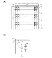
図1(A)は、液晶表示装置の構成例を示す図である。図1(A)に示す液晶表示装置は、画素部10と、走査線駆動回路11と、信号線駆動回路12と、各々が平行又は略平行に配設され、且つ走査線駆動回路11によって電位が制御されるm本の走査線13と、各々が平行又は略平行に配設され、且つ信号線駆動回路12によって電位が制御される、n本の信号線14と、を有する。さらに、画素部10は、3つの領域(領域101〜領域103)に分割され、領域毎にマトリクス状に配設された複数の画素を有する。なお、各走査線13は、画素部10においてm行n列に配設された複数の画素のうち、いずれかの行に配設されたn個の画素に電気的に接続される。また、各信号線14は、m行n列に配設された複数の画素のうち、いずれかの列に配設されたm個の画素に電気的に接続される。
図2(A)は、図1(A)に示す液晶表示装置が有する走査線駆動回路11の構成例を示す図である。図2(A)に示す走査線駆動回路11は、第1の走査線駆動回路用クロック信号(GCK1)を供給する配線乃至第4の走査線駆動回路用クロック信号(GCK4)を供給する配線と、第1のパルス幅制御信号(PWC1)を供給する配線乃至第6のパルス幅制御信号(PWC6)を供給する配線と、1行目に配設された走査線13に電気的に接続された第1のパルス出力回路20_1、乃至、m行目に配設された走査線13に電気的に接続された第mのパルス出力回路20_mと、を有する。なお、ここでは、第1のパルス出力回路20_1〜第kのパルス出力回路20_k(kは、m/2未満の4の倍数)が、領域101に配設された走査線13に電気的に接続され、第k+1のパルス出力回路20_k+1〜第2kのパルス出力回路20_2kが、領域102に配設された走査線13に電気的に接続され、第2k+1のパルス出力回路20_2k+1〜第mのパルス出力回路20_mが領域103に配設された走査線13に電気的に接続されることとする。また、第1のパルス出力回路20_1乃至第mのパルス出力回路20_mは、第1のパルス出力回路20_1に入力される走査線駆動回路用スタートパルス(GSP)をきっかけとしてシフト期間毎にシフトパルスを順次シフトする機能を有する。さらに、第1のパルス出力回路20_1乃至第mのパルス出力回路20_mにおいて複数のシフトパルスのシフトを並行して行うことが可能である。すなわち、第1のパルス出力回路20_1乃至第mのパルス出力回路20_mにおいてシフトパルスのシフトが行われている期間内であっても、第1のパルス出力回路20_1に走査線駆動回路用スタートパルス(GSP)を入力することが可能である。
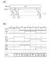
図3(A)は、図2(A)、(C)に示すパルス出力回路の構成例を示す図である。図3(A)に示すパルス出力回路は、トランジスタ31乃至トランジスタ39を有する。
上述したパルス出力回路の動作例について図3(B)〜(D)を参照して説明する。なお、ここでは、第1のパルス出力回路20_1の端子21に入力される走査線駆動回路用スタートパルス(GSP)の入力タイミングを制御することで、第1のパルス出力回路20_1、第(k+1)のパルス出力回路20_k+1、及び第(2k+1)のパルス出力回路20_2k+1の端子27から同一タイミングでシフトパルスを出力する場合の動作例について説明する。具体的には、図3(B)は、走査線駆動回路用スタートパルス(GSP)が入力される際の第1のパルス出力回路20_1の各端子に入力される信号の電位、並びにノードA及びノードBの電位を示しており、図3(C)は、第kのパルス出力回路20_kからハイレベルの電位が入力される際の第(k+1)のパルス出力回路20_k+1の各端子に入力される信号の電位、並びにノードA及びノードBの電位を示しており、図3(D)は、第2kのパルス出力回路20_2kからハイレベルの電位が入力される際の第(2k+1)のパルス出力回路20_2k+1の各端子に入力される信号の電位、並びにノードA及びノードBの電位を示している。なお、図3(B)〜(D)では、各端子に入力される信号を括弧書きで付記している。また、それぞれの後段に配設されるパルス出力回路(第2のパルス出力回路20_2、第(k+2)のパルス出力回路20_k+2、第(2k+2)のパルス出力回路20_2k+2)の端子25から出力される信号(Gout2、Goutk+2、Gout2k+2)及び端子27の出力信号(SRout2=第1のパルス出力回路20_1の端子26の入力信号、SRoutk+2=第(k+1)のパルス出力回路20_k+1の端子26の入力信号、SRout2k+2=第(2k+1)のパルス出力回路20_2k+1の端子26の入力信号)も付記している。なお、図中において、Goutは、パルス出力回路の走査線に対する出力信号を表し、SRoutは、当該パルス出力回路の、後段のパルス出力回路に対する出力信号を表している。
図4(A)は、図1(A)に示す液晶表示装置が有する信号線駆動回路12の構成例を示す図である。図4(A)に示す信号線駆動回路12は、第1の出力端子乃至第nの出力端子を有するシフトレジスタ120と、画像信号(DATA)を供給する配線と、ソース及びドレインの一方が画像信号(DATA)を供給する配線に電気的に接続され、ソース及びドレインの他方が画素部において1列目に配設された信号線14_1に電気的に接続され、ゲートがシフトレジスタ120の第1の出力端子に電気的に接続されたトランジスタ121_1、乃至、ソース及びドレインの一方が画像信号(DATA)を供給する配線に電気的に接続され、ソース及びドレインの他方が画素部においてn列目に配設された信号線14_nに電気的に接続され、ゲートがシフトレジスタ120の第nの出力端子に電気的に接続されたトランジスタ121_nと、を有する。なお、シフトレジスタ120は、信号線駆動回路用スタートパルス(SSP)をきっかけとしてシフト期間毎に順次第1の出力端子乃至第nの出力端子からハイレベルの電位を出力する機能を有する。すなわち、トランジスタ121_1乃至トランジスタ121_nは、シフト期間毎に順次オン状態となる。
図5は、図1(A)に示す液晶表示装置の画素部10の後方に設けられるバックライトパネル40の構成例を示す図である。図5(A)に示すバックライトパネル40は、複数のバックライトアレイ41を列方向に並べて備え、それぞれのバックライトアレイ41は、赤(R)、緑(G)、青(B)の3色を呈する光源を含むバックライトユニット42を複数並べて備える。なお、複数のバックライトユニット42は、特定の領域毎に点灯を制御することが可能であればよく、画素部10の後方に例えばマトリクス状に配設すればよい。
液晶表示装置に入力された映像信号V(data)を、画像処理回路70を介して、液晶パネル19と、バックライトパネル40に出力する構成の一例を、図16を用いて説明する。
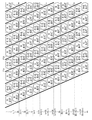
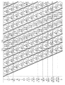
図6は、上述した液晶表示装置における選択信号の走査と、バックライトが有する1行目乃至t行目用バックライトアレイ41a1〜2k+3t+1行目乃至m行目用バックライトアレイ41c4の点灯タイミングとを示す図である。なお、図6において縦軸は画素部における行(1行目乃至m行目)を表し、横軸は時間を表している。図6に示すように当該液晶表示装置では、1行目に配設された走査線〜m行目に配設された走査線に対して順次選択信号を供給するのではなく、k行分隔離されて配設された走査線に対して順次選択信号を供給する(1行目に配設された走査線→k+1行目に配設された走査線→2k+1行目に配設された走査線→2行目に配設された走査線という順序で選択信号を供給する)ことが可能である。そのため、期間(T1)において、1行目に配設されたn個の画素からt行目に配設されたn個の画素を順次選択し、且つk+1行目に配設されたn個の画素からk+t行目に配設されたn個の画素を順次選択し、且つ2k+1行目に配設されたn個の画素から2k+t行目に配設されたn個の画素を順次選択することで、各画素に画像信号を入力することが可能である。なお、ここでは、1行目に配設されたn個の画素乃至t行目に配設されたn個の画素には、赤(R)を呈する光の透過を制御する画像信号が入力され、k+1行目に配設されたn個の画素乃至k+t行目に配設されたn個の画素には、青(B)を呈する光の透過を制御する画像信号が入力され、2k+1行目に配設されたn個の画素乃至2k+t行目に配設されたn個の画素には、緑(G)を呈する光の透過を制御する画像信号が入力されることとする。
本実施の形態の液晶表示装置は、画像信号の入力と、バックライトの点灯とを並行して行うことが可能である。そのため、当該液晶表示装置の各画素に対する画像信号の入力頻度を向上させることなどが可能になる。その結果、フィールドシーケンシャル方式によって表示を行う液晶表示装置において生じるカラーブレイクを抑制し、該液晶表示装置が表示する画質を向上させることが可能である。
本実施の形態の液晶表示装置は、本発明の一態様であり、当該液晶表示装置と異なる点を有する液晶表示装置も本発明には含まれる。
本実施の形態では、実施の形態1に示した液晶表示装置の具体的な構成について、説明する。
まず、上述した液晶表示装置の画素部又は各種回路に用いられるトランジスタの具体例について図17を参照して説明する。なお、当該液晶表示装置において、画素部及び各種回路のそれぞれに設けられるトランジスタは、同一構成を有するトランジスタを適用してもよいし、それぞれ異なる構成を有するトランジスタを適用してもよい。
次いで、上述した液晶表示装置の画素のレイアウトの具体例について図18、19を参照して説明する。なお、図18は、図1(B)に示した画素のレイアウトの上面図を示す図であり、図19は、図18に示すA−B線における断面図を示す図である。なお、図18においては、液晶層、対向電極などの構成は割愛している。以下、具体的な構造について図19を参照して説明する。
次いで、液晶表示装置のパネルの外観について、図20を用いて説明する。図20(A)は、基板4001と対向基板4006とをシール材4005によって接着させたパネルの上面図であり、図20(B)は、図20(A)のC−D線における断面図に相当する。
以下では、本明細書で開示される液晶表示装置を搭載した電子機器の例について図22を参照して説明する。
本実施の形態では、本発明の一態様に係る液晶表示装置において用いられる、基板の一形態について図23、24を参照して説明する。
上述した構成を有する表示装置は、本発明の一態様であり、当表示装置と異なる構成を備える以下の表示装置も、本発明に含まれる。上述の転置工程(図23(B)参照)の後、転置基板6110を貼り付ける前に、露出した剥離層6201、若しくは被剥離層6116表面に、金属板6206を貼り付けても良い(図23(C’)参照)。この場合、金属板6206からの汚染物質が、被剥離層6116におけるトランジスタの特性に悪影響を及ぼすことを防ぐため、バリア層6207を間に設けると良い。バリア層6207を設ける場合は、露出した剥離層6201、または被剥離層6116表面にバリア層6207を設けてから、金属板6206を貼り付ければ良い。バリア層6207は無機材料や有機材料などにより形成すれば良く、代表的には窒化シリコンなどが挙げられるが、トランジスタの汚染を防止することができれば、これらに限られることはない。バリア層6207は透光性を有する材料で形成するか、もしくは透光性を有する程度に薄い膜とするなど、少なくとも可視光に対する透光性を有するように作製する。なお、金属板6206は、剥離用接着剤6203とは異なる接着剤を用いて第2の接着剤層(図示せず)を形成し、接着すればよい。
11 走査線駆動回路
12 信号線駆動回路
13 走査線
14 信号線
15 画素
16 トランジスタ
17 容量素子
18 液晶素子
19 液晶パネル
20 パルス出力回路
21 端子
22 端子
23 端子
24 端子
25 端子
26 端子
27 端子
31 トランジスタ
32 トランジスタ
33 トランジスタ
34 トランジスタ
35 トランジスタ
36 トランジスタ
37 トランジスタ
38 トランジスタ
39 トランジスタ
40 バックライトパネル
41 バックライトアレイ
41a1 バックライトアレイ
41a2 バックライトアレイ
41a3 バックライトアレイ
41a4 バックライトアレイ
41b1 バックライトアレイ
41c1 バックライトアレイ
41c4 バックライトアレイ
42 バックライトユニット
45 バックライト駆動回路
46a パルス幅変調回路
50 トランジスタ
51 トランジスタ
52 トランジスタ
53 トランジスタ
70 画像処理回路
71 ADコンバータ
72 フレームメモリ
73 最大値検出回路
73a 最大値検出回路
73b 最大値検出回路
73c 最大値検出回路
74 ガンマ補正回路
74a ガンマ補正回路
74b ガンマ補正回路
74c ガンマ補正回路
101 領域
102 領域
103 領域
120 シフトレジスタ
121 トランジスタ
220 基板
221 絶縁層
222 導電層
223 絶縁層
224 半導体層
225a 導電層
225b 導電層
226 導電層
227 絶縁層
228 導電層
229 絶縁層
230 平坦化絶縁層
231 透明導電層
240 対向基板
241 透明導電層
242 遮蔽層
250 液晶層
265 透明導電層
1601 パネル
1602 拡散板
1603 プリズムシート
1604 拡散板
1605 導光板
1607 バックライトパネル
1608 回路基板
1609 COFテープ
1610 FPC
1611 基板
1612 バックライト
2201 本体
2202 筐体
2203 表示部
2204 キーボード
2211 本体
2212 スタイラス
2213 表示部
2214 操作ボタン
2215 外部インターフェイス
2220 電子書籍
2221 筐体
2223 筐体
2225 表示部
2227 表示部
2231 電源
2233 操作キー
2235 スピーカー
2237 軸部
2240 筐体
2241 筐体
2242 表示パネル
2243 スピーカー
2244 マイクロフォン
2245 操作キー
2246 ポインティングデバイス
2247 カメラ用レンズ
2248 外部接続端子
2249 太陽電池セル
2250 外部メモリスロット
2261 本体
2263 接眼部
2264 操作スイッチ
2265 表示部(B)
2266 バッテリー
2267 表示部(A)
2270 テレビジョン装置
2271 筐体
2273 表示部
2275 スタンド
2277 表示部
2279 操作キー
2280 リモコン操作機
2400 基板
2401 ゲート層
2402 ゲート絶縁層
2403 半導体層
2405a ソース層
2405b ドレイン層
2406 チャネル保護層
2407 絶縁層
2409 保護絶縁層
2411 ゲート層
2412 ゲート層
2413 ゲート絶縁層
2414 ゲート絶縁層
2436 下地層
2450 トランジスタ
2460 トランジスタ
2470 トランジスタ
2480 トランジスタ
4001 基板
4002 画素部
4003 信号線駆動回路
4004 走査線駆動回路
4005 シール材
4006 対向基板
4007 液晶
4009 トランジスタ
4010 トランジスタ
4011 液晶素子
4014 配線
4015 配線
4016 接続端子
4018 FPC
4019 異方性導電膜
4021 基板
4022 トランジスタ
4030 画素電極
4031 対向電極
4035 スペーサ
6110 転置基板
6111 接着剤層
6116 被剥離層
6200 作製基板
6201 剥離層
6202 仮支持基板
6203 剥離用接着剤
6206 金属板
6207 バリア層
6210 配線層
6211 配線層
6212 領域
Claims (4)
- m行n列(m、nは、4以上の自然数)のマトリクス状に配設された複数の画素とその後方に設けられるバックライトを備え且つ同じ列に配設された複数の画素は同じ信号線と電気的に接続される液晶表示装置の1行目乃至A行目(Aは、m/2以下の自然数)にマトリクス状に配設された複数の画素に対して、第1の色を呈する光の透過を制御するための画像信号を入力し、且つA+1行目乃至2A行目にマトリクス状に配設された複数の画素に対して第2の色を呈する光の透過を制御するための画像信号を入力する期間に、
前記第1の色を呈する光の透過を制御するための画像信号であって、1行目乃至B行目(Bは、A/2以下の自然数)に配設された複数の画素に係るものの中から、最大値検出回路を用いて第1の最も明るい階調の第1の画像信号を検出し、前記第1の画像信号を表示する第1の画素の透過率を最大とし、前記第1の最も明るい階調に比べて階調が暗くなる割合に応じて画素の透過率を低減するようにガンマ補正して、前記第1の色を呈する光の透過を制御するための画像信号を1行目乃至B行目に配設された複数の画素に出力するステップと、
前記第2の色を呈する光の透過を制御するための画像信号であって、A+1行目乃至A+B行目に配設された複数の画素に係るものの中から、最大値検出回路を用いて第2の最も明るい階調の第2の画像信号を検出し、前記第2の画像信号を表示する第2の画素の透過率を最大とし、前記第2の最も明るい階調に比べて階調が暗くなる割合に応じて画素の透過率を低減するようにガンマ補正して、前記第2の色を呈する光の透過を制御するための画像信号をA+1行目乃至A+B行目に配設された複数の画素に出力するステップを備え、
s行目(sはA未満の自然数)に配設された複数の画素及びA+s行目に配接された複数の画素にs行目に配設された複数の画素用の画像信号が出力された後に、A+s行目に配接された複数の画素にA+s行目に配接された複数の画素用の画像信号が出力され、
次いで、前記1行目乃至B行目に配設された複数の画素に、透過率が最大の前記第1の画素において前記第1の画像信号に相当する階調の表示が行われる強さで前記第1の色を呈する光を、前記A+1行目乃至A+B行目に配設された複数の画素に、透過率が最大の前記第2の画素において前記第2の画像信号に相当する階調の表示が行われる強さで前記第2の色を呈する光を、同時に照射するステップを備える液晶表示装置の駆動方法。 - m行n列(m、nは、4以上の自然数)のマトリクス状に配設された複数の画素とその後方に設けられるバックライトを備え且つ同じ列に配設された複数の画素は同じ信号線と電気的に接続される液晶表示装置の1行目乃至A行目(Aは、m/2以下の自然数)に配設された複数の画素に対して、第1の色を呈する光の透過を制御するための画像信号を入力し、且つA+1行目乃至2A行目に配設された複数の画素に対して第2の色を呈する光の透過を制御するための画像信号を入力する期間に、
1行目乃至A行目をp個(pは2以上の自然数)に分割したいずれか一の第1の領域に配設された複数の画素に前記第1の色を呈する光の透過を制御するための画像信号の中から、最大値検出回路を用いて最も明るい階調の第1の画像信号を検出し、前記第1の画像信号を表示する画素の透過率を最大とし、前記第1の最も明るい階調に比べて階調が暗くなる割合に応じて画素の透過率を低減するようにガンマ補正して、前記第1の色を呈する光の透過を制御するための画像信号を前記第1の領域に出力するステップと、
A+1行目乃至2A行目をq個(qは2以上の自然数)に分割したいずれか一の第2の領域に配設された複数の画素に前記第2の色を呈する光の透過を制御するための画像信号の中から、最大値検出回路を用いて最も明るい階調の第2の画像信号を検出し、前記第2の画像信号を表示する画素の透過率を最大とし、前記第2の最も明るい階調に比べて階調が暗くなる割合に応じて画素の透過率を低減するようにガンマ補正して、前記第2の色を呈する光の透過を制御するための画像信号を前記第2の領域に出力するステップを備え、
s行目(sはA未満の自然数)に配設された複数の画素及びA+s行目に配接された複数の画素にs行目に配設された複数の画素用の画像信号が出力された後に、A+s行目に配接された複数の画素にA+s行目に配接された複数の画素用の画像信号が出力され、
次いで、前記p個の領域を独立して照明できる光源が接続された第1のパルス幅変調回路を用いて、1/(p−1)以下のデューティー比で、前記第1の領域に配設された透過率が最大の画素において前記第1の画像信号に相当する階調の表示が行われるように前記第1の色を呈する光を照射し、前記q個の領域を独立して照明できる光源が接続された第2のパルス幅変調回路を用いて、1/(q−1)以下のデューティー比で、前記第2の領域に配設された、透過率が最大の画素において前記第2の画像信号に相当する階調の表示が行われるように前記第2の色を呈する光を照射するステップを備える液晶表示装置の駆動方法。 - 請求項1又は請求項2において、
走査線駆動回路を有し、
前記走査線駆動回路は、第1乃至第mのパルス出力回路を有し、
前記第Aのパルス出力回路からシフトパルスが出力されるタイミングと同じタイミングで、スタートパルスを前記走査線駆動回路に入力することを特徴とする液晶表示装置の駆動方法。 - 請求項1乃至請求項3のいずれか一項において、
前記複数の画素は、トランジスタを有し、
前記トランジスタのチャネル形成領域は、化学量論的組成比より酸素が多い絶縁層と接する酸化物半導体を有することを特徴とする液晶表示装置の駆動方法。
Priority Applications (1)
| Application Number | Priority Date | Filing Date | Title |
|---|---|---|---|
| JP2011142652A JP5889552B2 (ja) | 2010-07-02 | 2011-06-28 | 液晶表示装置の駆動方法 |
Applications Claiming Priority (3)
| Application Number | Priority Date | Filing Date | Title |
|---|---|---|---|
| JP2010152411 | 2010-07-02 | ||
| JP2010152411 | 2010-07-02 | ||
| JP2011142652A JP5889552B2 (ja) | 2010-07-02 | 2011-06-28 | 液晶表示装置の駆動方法 |
Related Child Applications (1)
| Application Number | Title | Priority Date | Filing Date |
|---|---|---|---|
| JP2016027698A Division JP6215980B2 (ja) | 2010-07-02 | 2016-02-17 | 表示装置及び表示装置の作製方法 |
Publications (2)
| Publication Number | Publication Date |
|---|---|
| JP2012032798A JP2012032798A (ja) | 2012-02-16 |
| JP5889552B2 true JP5889552B2 (ja) | 2016-03-22 |
Family
ID=45399475
Family Applications (2)
| Application Number | Title | Priority Date | Filing Date |
|---|---|---|---|
| JP2011142652A Expired - Fee Related JP5889552B2 (ja) | 2010-07-02 | 2011-06-28 | 液晶表示装置の駆動方法 |
| JP2016027698A Active JP6215980B2 (ja) | 2010-07-02 | 2016-02-17 | 表示装置及び表示装置の作製方法 |
Family Applications After (1)
| Application Number | Title | Priority Date | Filing Date |
|---|---|---|---|
| JP2016027698A Active JP6215980B2 (ja) | 2010-07-02 | 2016-02-17 | 表示装置及び表示装置の作製方法 |
Country Status (5)
| Country | Link |
|---|---|
| US (1) | US9230489B2 (ja) |
| JP (2) | JP5889552B2 (ja) |
| CN (2) | CN102971784B (ja) |
| TW (2) | TWI534786B (ja) |
| WO (1) | WO2012002165A1 (ja) |
Families Citing this family (35)
| Publication number | Priority date | Publication date | Assignee | Title |
|---|---|---|---|---|
| US20120313985A1 (en) * | 2010-03-30 | 2012-12-13 | Sharp Kabushiki Kaisha | Liquid crystal display device and liquid crystal display method |
| TWI562109B (en) | 2010-08-05 | 2016-12-11 | Semiconductor Energy Lab Co Ltd | Driving method of liquid crystal display device |
| JP2012103683A (ja) | 2010-10-14 | 2012-05-31 | Semiconductor Energy Lab Co Ltd | 表示装置及び表示装置の駆動方法 |
| KR101850990B1 (ko) * | 2011-07-06 | 2018-04-23 | 삼성디스플레이 주식회사 | 표시 장치 및 그 구동 방법 |
| KR20130006165A (ko) * | 2011-07-08 | 2013-01-16 | 삼성전자주식회사 | 터치 인식 방법 및 이를 적용한 디스플레이 시스템 |
| JP2014032399A (ja) | 2012-07-13 | 2014-02-20 | Semiconductor Energy Lab Co Ltd | 液晶表示装置 |
| KR102481056B1 (ko) | 2012-08-10 | 2022-12-27 | 가부시키가이샤 한도오따이 에네루기 켄큐쇼 | 반도체 장치 및 전자 장치 |
| US9728115B2 (en) * | 2013-05-13 | 2017-08-08 | Sharp Kabushiki Kaisha | Liquid crystal display device and data correction method in liquid crystal display device |
| KR20150081174A (ko) * | 2014-01-03 | 2015-07-13 | 삼성디스플레이 주식회사 | 액정표시장치 및 이의 구동방법 |
| WO2016002424A1 (ja) * | 2014-07-04 | 2016-01-07 | シャープ株式会社 | 液晶表示装置 |
| CN104133313A (zh) * | 2014-06-18 | 2014-11-05 | 京东方科技集团股份有限公司 | 阵列基板及其制备方法、液晶显示装置 |
| KR20170093832A (ko) * | 2014-11-28 | 2017-08-16 | 가부시키가이샤 한도오따이 에네루기 켄큐쇼 | 화상 처리 장치, 표시 시스템, 및 전자 기기 |
| US11471752B2 (en) * | 2014-12-04 | 2022-10-18 | Dov Rotshtain | Computer-controlled board games |
| CN104505030B (zh) * | 2014-12-24 | 2017-12-26 | 深圳市华星光电技术有限公司 | 一种背光驱动电路及其驱动方法和液晶显示装置 |
| US10326919B2 (en) * | 2016-10-19 | 2019-06-18 | Olympus Corporation | Method for manufacturing endoscope image pickup module, endoscope image pickup module and endoscope |
| CN108711403B (zh) * | 2016-11-10 | 2021-10-29 | 拉碧斯半导体株式会社 | 显示驱动器以及半导体装置 |
| CN107039007A (zh) * | 2017-06-19 | 2017-08-11 | 深圳天珑无线科技有限公司 | 一种背光亮度调整的方法及装置 |
| WO2019008464A1 (en) * | 2017-07-07 | 2019-01-10 | Semiconductor Energy Laboratory Co., Ltd. | METHOD FOR ATTACKING A DISPLAY PANEL |
| JP6995598B2 (ja) * | 2017-12-12 | 2022-01-14 | 株式会社ジャパンディスプレイ | 表示装置 |
| KR20250151580A (ko) * | 2018-05-18 | 2025-10-21 | 가부시키가이샤 한도오따이 에네루기 켄큐쇼 | 표시 장치 및 표시 장치의 구동 방법 |
| CN119403406A (zh) | 2018-06-06 | 2025-02-07 | 株式会社半导体能源研究所 | 显示装置、显示模块及电子设备 |
| CN208538435U (zh) * | 2018-08-01 | 2019-02-22 | 京东方科技集团股份有限公司 | 一种显示装置 |
| US11107424B2 (en) * | 2018-09-18 | 2021-08-31 | Apple Inc. | Backlight noise reduction systems and methods for electronic device displays |
| US11081070B2 (en) * | 2018-09-18 | 2021-08-03 | Apple Inc. | Backlight systems and methods for electronic device displays |
| CN209345209U (zh) * | 2019-03-08 | 2019-09-03 | Oppo广东移动通信有限公司 | 电子设备 |
| CN110400544A (zh) * | 2019-08-05 | 2019-11-01 | 业成科技(成都)有限公司 | 讯号处理方法及显示装置 |
| CN110707096A (zh) * | 2019-09-18 | 2020-01-17 | 深圳市华星光电半导体显示技术有限公司 | 一种阵列基板及其制备方法、显示装置 |
| CN112684631A (zh) * | 2019-10-18 | 2021-04-20 | 群创光电股份有限公司 | 显示装置 |
| JP7410684B2 (ja) * | 2019-10-21 | 2024-01-10 | シャープ株式会社 | マイクシステム |
| CN112083339B (zh) * | 2020-09-13 | 2024-04-30 | 巨安储能武汉科技有限责任公司 | 一种电池荷电状态监测方法 |
| TWI798964B (zh) * | 2021-11-29 | 2023-04-11 | 瑞昱半導體股份有限公司 | 顯示裝置與相關的系統晶片 |
| JP7639146B2 (ja) | 2022-07-20 | 2025-03-04 | 綿陽恵科光電科技有限公司 | バックライト駆動回路、バックライトモジュール及び表示装置 |
| CN115035867B (zh) * | 2022-07-20 | 2023-04-28 | 绵阳惠科光电科技有限公司 | 背光驱动电路及方法、背光模组以及显示装置 |
| US20250194277A1 (en) * | 2023-12-07 | 2025-06-12 | Taiwan Semiconductor Manufacturing Company, Ltd. | Image sensor device with light retention structure |
| TWI876852B (zh) * | 2024-01-26 | 2025-03-11 | 瀚宇彩晶股份有限公司 | 顯示器及顯示器的階調調整方法 |
Family Cites Families (82)
| Publication number | Priority date | Publication date | Assignee | Title |
|---|---|---|---|---|
| JPS62278537A (ja) * | 1986-05-27 | 1987-12-03 | Toshiba Corp | アクテイブマトリツクス型表示装置用表示電極アレイ |
| US5126865A (en) * | 1990-12-31 | 1992-06-30 | Honeywell Inc. | Liquid crystal display with sub-pixels |
| GB9110737D0 (en) * | 1991-05-17 | 1991-07-10 | Philips Electronic Associated | Method of fabricating mim type device arrays and display devices incorporating such arrays |
| JPH05335424A (ja) * | 1992-05-28 | 1993-12-17 | Alps Electric Co Ltd | 絶縁層を介した上部電極と下部電極の導通方法及びその構造 |
| JPH06222330A (ja) | 1993-01-25 | 1994-08-12 | Hitachi Ltd | 液晶表示装置 |
| JP3371200B2 (ja) | 1997-10-14 | 2003-01-27 | 富士通株式会社 | 液晶表示装置の表示制御方法及び液晶表示装置 |
| JP3280307B2 (ja) * | 1998-05-11 | 2002-05-13 | インターナショナル・ビジネス・マシーンズ・コーポレーション | 液晶表示装置 |
| EP0997868B1 (en) | 1998-10-30 | 2012-03-14 | Semiconductor Energy Laboratory Co., Ltd. | Field sequential liquid crystal display device and driving method thereof, and head mounted display |
| US6597348B1 (en) | 1998-12-28 | 2003-07-22 | Semiconductor Energy Laboratory Co., Ltd. | Information-processing device |
| JP3683463B2 (ja) * | 1999-03-11 | 2005-08-17 | シャープ株式会社 | アクティブマトリクス基板、その製造方法、及び、該基板を用いたイメージセンサ |
| JP2000275605A (ja) * | 1999-03-25 | 2000-10-06 | Toshiba Corp | 液晶表示装置 |
| US7145536B1 (en) | 1999-03-26 | 2006-12-05 | Semiconductor Energy Laboratory Co., Ltd. | Liquid crystal display device |
| JP3592205B2 (ja) | 1999-07-23 | 2004-11-24 | 日本電気株式会社 | 液晶表示装置の駆動方法 |
| KR100347558B1 (ko) | 1999-07-23 | 2002-08-07 | 닛본 덴기 가부시끼가이샤 | 액정표시장치 및 그 구동방법 |
| US6882012B2 (en) | 2000-02-28 | 2005-04-19 | Semiconductor Energy Laboratory Co., Ltd. | Semiconductor device and a method of manufacturing the same |
| TW521237B (en) | 2000-04-18 | 2003-02-21 | Semiconductor Energy Lab | Light emitting device |
| TWI267049B (en) | 2000-05-09 | 2006-11-21 | Sharp Kk | Image display device, and electronic apparatus using the same |
| TW518552B (en) | 2000-08-18 | 2003-01-21 | Semiconductor Energy Lab | Liquid crystal display device, method of driving the same, and method of driving a portable information device having the liquid crystal display device |
| JP3770380B2 (ja) | 2000-09-19 | 2006-04-26 | シャープ株式会社 | 液晶表示装置 |
| US7385579B2 (en) | 2000-09-29 | 2008-06-10 | Semiconductor Energy Laboratory Co., Ltd. | Liquid crystal display device and method of driving the same |
| US6801220B2 (en) | 2001-01-26 | 2004-10-05 | International Business Machines Corporation | Method and apparatus for adjusting subpixel intensity values based upon luminance characteristics of the subpixels for improved viewing angle characteristics of liquid crystal displays |
| JP2004077567A (ja) | 2002-08-09 | 2004-03-11 | Semiconductor Energy Lab Co Ltd | 表示装置及びその駆動方法 |
| JP2004094058A (ja) | 2002-09-02 | 2004-03-25 | Semiconductor Energy Lab Co Ltd | 液晶表示装置および液晶表示装置の駆動方法 |
| US7193593B2 (en) | 2002-09-02 | 2007-03-20 | Semiconductor Energy Laboratory Co., Ltd. | Liquid crystal display device and method of driving a liquid crystal display device |
| CN100580753C (zh) | 2002-11-29 | 2010-01-13 | 株式会社半导体能源研究所 | 显示装置和电子装置 |
| JP2004191490A (ja) | 2002-12-09 | 2004-07-08 | Hitachi Displays Ltd | 液晶表示装置 |
| US7176878B2 (en) | 2002-12-11 | 2007-02-13 | Nvidia Corporation | Backlight dimming and LCD amplitude boost |
| US8125601B2 (en) * | 2003-01-08 | 2012-02-28 | Samsung Electronics Co., Ltd. | Upper substrate and liquid crystal display device having the same |
| JP4493274B2 (ja) | 2003-01-29 | 2010-06-30 | 富士通株式会社 | 表示装置及び表示方法 |
| TWI251199B (en) | 2003-03-31 | 2006-03-11 | Sharp Kk | Image processing method and liquid-crystal display device using the same |
| TWI246048B (en) | 2003-06-17 | 2005-12-21 | Au Optronics Corp | Driving method of liquid crystal display |
| US8319219B2 (en) | 2003-07-14 | 2012-11-27 | Semiconductor Energy Laboratory Co., Ltd. | Light-emitting device |
| JP2005115287A (ja) * | 2003-10-10 | 2005-04-28 | Nec Electronics Corp | 表示装置の駆動回路およびその駆動方法 |
| CN100557667C (zh) | 2004-04-22 | 2009-11-04 | 株式会社半导体能源研究所 | 发光装置及其驱动方法 |
| JP2005316092A (ja) | 2004-04-28 | 2005-11-10 | Casio Comput Co Ltd | フィールドシーケンシャル液晶表示装置 |
| US20070216616A1 (en) | 2004-06-01 | 2007-09-20 | Koninklijke Philips Electronics, N.V. | Display Device Comprising A Light Source |
| JP2006047594A (ja) | 2004-08-03 | 2006-02-16 | Funai Electric Co Ltd | 液晶表示装置 |
| KR101460089B1 (ko) * | 2004-12-23 | 2014-11-10 | 돌비 레버러토리즈 라이쎈싱 코오포레이션 | 폭넓은 색상 범위 디스플레이, 및 관찰 영역에 이미지를 표시하기 위한 장치 및 방법 |
| JP2006220685A (ja) | 2005-02-08 | 2006-08-24 | 21 Aomori Sangyo Sogo Shien Center | スキャンバックライトを用いた分割駆動フィールドシーケンシャルカラー液晶ディスプレイの駆動方法および装置 |
| JP4559985B2 (ja) | 2005-03-15 | 2010-10-13 | 株式会社東芝 | 乱数発生回路 |
| JP4560502B2 (ja) | 2005-09-06 | 2010-10-13 | キヤノン株式会社 | 電界効果型トランジスタ |
| JP2007114628A (ja) | 2005-10-24 | 2007-05-10 | Rohm Co Ltd | バックライト装置およびこれを用いた画像表示装置 |
| KR101106561B1 (ko) | 2005-12-19 | 2012-01-19 | 엘지디스플레이 주식회사 | 액정표시장치의 구동회로 및 이를 포함하는 액정표시장치 |
| EP1832915B1 (en) | 2006-01-31 | 2012-04-18 | Semiconductor Energy Laboratory Co., Ltd. | Display device with improved contrast |
| JP2007219510A (ja) * | 2006-02-13 | 2007-08-30 | Samsung Electronics Co Ltd | ディスプレイ装置 |
| JP2007264211A (ja) | 2006-03-28 | 2007-10-11 | 21 Aomori Sangyo Sogo Shien Center | 色順次表示方式液晶表示装置用の色表示方法 |
| US8106865B2 (en) | 2006-06-02 | 2012-01-31 | Semiconductor Energy Laboratory Co., Ltd. | Display device and driving method thereof |
| US8154493B2 (en) | 2006-06-02 | 2012-04-10 | Semiconductor Energy Laboratory Co., Ltd. | Liquid crystal display device, driving method of the same, and electronic device using the same |
| EP1898676A1 (en) | 2006-09-06 | 2008-03-12 | THOMSON Licensing | Display apparatus |
| US7941471B2 (en) | 2007-01-29 | 2011-05-10 | International Business Machines Corporation | Differential approach to current-mode chaos based random number generator |
| US20080238336A1 (en) | 2007-03-29 | 2008-10-02 | Hong Kong Applied Science And Technology Research | Back-Light Devices and Displays Incorporating Same |
| KR100885285B1 (ko) | 2007-05-08 | 2009-02-23 | 닛뽕빅터 가부시키가이샤 | 액정 표시 장치 및 이에 이용되는 영상 표시 방법 |
| US8139022B2 (en) | 2007-05-08 | 2012-03-20 | Victor Company Of Japan, Limited | Liquid crystal display device and image display method thereof |
| CN101303839A (zh) * | 2007-05-08 | 2008-11-12 | 日本胜利株式会社 | 液晶显示装置及用于该装置的影像显示方法 |
| JP2009042652A (ja) | 2007-08-10 | 2009-02-26 | Victor Co Of Japan Ltd | 液晶表示装置及びこれに用いる映像表示方法 |
| KR100867104B1 (ko) | 2007-07-27 | 2008-11-06 | 전자부품연구원 | 영상 표시 장치의 백라이트 밝기 제어 방법 및 장치 |
| JP5200209B2 (ja) | 2007-08-08 | 2013-06-05 | エプソンイメージングデバイス株式会社 | 液晶表示装置 |
| JP5235363B2 (ja) * | 2007-09-04 | 2013-07-10 | 株式会社ジャパンディスプレイイースト | 液晶表示装置 |
| JP4308293B2 (ja) | 2007-11-20 | 2009-08-05 | 際国 董 | 乱数生成装置及び方法 |
| US20090167670A1 (en) | 2007-12-26 | 2009-07-02 | Hong Kong Applied Science and Technology Research Institute Company Limited | Method of determining luminance values for a backlight of an lcd panel displaying an image |
| KR20090091534A (ko) | 2008-02-25 | 2009-08-28 | 엘지전자 주식회사 | 액정표시장치의 백라이트 보정 방법 및 그 액정표시장치 |
| US8063873B2 (en) | 2008-02-29 | 2011-11-22 | Research In Motion Limited | System and method for adjusting a backlight level for a display on an electronic device |
| KR101404550B1 (ko) * | 2008-04-01 | 2014-06-09 | 삼성디스플레이 주식회사 | 액정 표시 장치 및 그 제조 방법 |
| KR100959594B1 (ko) | 2008-05-01 | 2010-05-27 | 닛뽕빅터 가부시키가이샤 | 액정 표시 장치 및 이에 이용되는 영상 표시 방법 |
| JP2010044180A (ja) | 2008-08-12 | 2010-02-25 | Victor Co Of Japan Ltd | 液晶表示装置及びこれに用いる映像信号処理方法 |
| KR100958006B1 (ko) * | 2008-06-18 | 2010-05-17 | 삼성모바일디스플레이주식회사 | 박막 트랜지스터, 그의 제조 방법 및 박막 트랜지스터를구비하는 평판 표시 장치 |
| KR101703511B1 (ko) | 2008-06-27 | 2017-02-07 | 가부시키가이샤 한도오따이 에네루기 켄큐쇼 | 박막 트랜지스터 |
| JP2010056541A (ja) * | 2008-07-31 | 2010-03-11 | Semiconductor Energy Lab Co Ltd | 半導体装置およびその作製方法 |
| JP5590868B2 (ja) | 2008-12-11 | 2014-09-17 | 株式会社半導体エネルギー研究所 | 半導体装置 |
| KR20100071325A (ko) * | 2008-12-19 | 2010-06-29 | 삼성전자주식회사 | 광원 구동 방법, 이를 수행하기 위한 광원 장치 및 이 광원장치를 포함하는 표시 장치 |
| JP5100670B2 (ja) | 2009-01-21 | 2012-12-19 | 株式会社半導体エネルギー研究所 | タッチパネル、電子機器 |
| TWI496042B (zh) | 2009-07-02 | 2015-08-11 | Semiconductor Energy Lab | 觸控面板及其驅動方法 |
| WO2011081010A1 (en) | 2009-12-28 | 2011-07-07 | Semiconductor Energy Laboratory Co., Ltd. | Liquid crystal display device and electronic device |
| KR101842865B1 (ko) | 2009-12-28 | 2018-03-28 | 가부시키가이샤 한도오따이 에네루기 켄큐쇼 | 액정 표시 장치 및 전자 기기 |
| US8830278B2 (en) | 2010-04-09 | 2014-09-09 | Semiconductor Energy Laboratory Co., Ltd. | Liquid crystal display device and method for driving the same |
| KR101748901B1 (ko) | 2010-04-09 | 2017-06-19 | 가부시키가이샤 한도오따이 에네루기 켄큐쇼 | 액정 표시 장치 및 그 구동 방법 |
| US8907881B2 (en) | 2010-04-09 | 2014-12-09 | Semiconductor Energy Laboratory Co., Ltd. | Liquid crystal display device and method for driving the same |
| CN103038813B (zh) | 2010-05-25 | 2016-07-27 | 株式会社半导体能源研究所 | 液晶显示装置及其驱动方法 |
| US8537086B2 (en) | 2010-06-16 | 2013-09-17 | Semiconductor Energy Laboratory Co., Ltd. | Driving method of liquid crystal display device |
| US8564529B2 (en) | 2010-06-21 | 2013-10-22 | Semiconductor Energy Laboratory Co., Ltd. | Method for driving liquid crystal display device |
| KR20130116857A (ko) | 2010-06-25 | 2013-10-24 | 가부시키가이샤 한도오따이 에네루기 켄큐쇼 | 액정 표시 장치 및 전자 기기 |
| US8988337B2 (en) | 2010-07-02 | 2015-03-24 | Semiconductor Energy Laboratory Co., Ltd. | Driving method of liquid crystal display device |
-
2011
- 2011-06-10 CN CN201180032159.6A patent/CN102971784B/zh not_active Expired - Fee Related
- 2011-06-10 WO PCT/JP2011/063855 patent/WO2012002165A1/en not_active Ceased
- 2011-06-10 CN CN201610399585.8A patent/CN106057144B/zh active Active
- 2011-06-23 US US13/167,045 patent/US9230489B2/en not_active Expired - Fee Related
- 2011-06-28 JP JP2011142652A patent/JP5889552B2/ja not_active Expired - Fee Related
- 2011-06-29 TW TW100122819A patent/TWI534786B/zh not_active IP Right Cessation
- 2011-06-29 TW TW105106140A patent/TWI579931B/zh active
-
2016
- 2016-02-17 JP JP2016027698A patent/JP6215980B2/ja active Active
Also Published As
| Publication number | Publication date |
|---|---|
| JP2016136261A (ja) | 2016-07-28 |
| US20120002133A1 (en) | 2012-01-05 |
| TW201624573A (zh) | 2016-07-01 |
| JP6215980B2 (ja) | 2017-10-18 |
| CN106057144A (zh) | 2016-10-26 |
| TWI579931B (zh) | 2017-04-21 |
| TW201220291A (en) | 2012-05-16 |
| WO2012002165A1 (en) | 2012-01-05 |
| CN106057144B (zh) | 2019-03-12 |
| JP2012032798A (ja) | 2012-02-16 |
| US9230489B2 (en) | 2016-01-05 |
| CN102971784A (zh) | 2013-03-13 |
| CN102971784B (zh) | 2016-08-03 |
| TWI534786B (zh) | 2016-05-21 |
Similar Documents
| Publication | Publication Date | Title |
|---|---|---|
| JP5889552B2 (ja) | 液晶表示装置の駆動方法 | |
| JP6152145B2 (ja) | 液晶表示装置 | |
| JP6145139B2 (ja) | 液晶表示装置の駆動方法 | |
| JP5798391B2 (ja) | 液晶表示装置の駆動方法 | |
| JP5973140B2 (ja) | 液晶表示装置の駆動方法 | |
| JP6078143B2 (ja) | 液晶表示装置 | |
| US9336727B2 (en) | Driving method of display device | |
| JP2012150455A (ja) | 液晶表示装置の駆動方法 |
Legal Events
| Date | Code | Title | Description |
|---|---|---|---|
| A621 | Written request for application examination |
Free format text: JAPANESE INTERMEDIATE CODE: A621 Effective date: 20140507 |
|
| A977 | Report on retrieval |
Free format text: JAPANESE INTERMEDIATE CODE: A971007 Effective date: 20150130 |
|
| A131 | Notification of reasons for refusal |
Free format text: JAPANESE INTERMEDIATE CODE: A131 Effective date: 20150203 |
|
| A521 | Written amendment |
Free format text: JAPANESE INTERMEDIATE CODE: A523 Effective date: 20150324 |
|
| A131 | Notification of reasons for refusal |
Free format text: JAPANESE INTERMEDIATE CODE: A131 Effective date: 20150818 |
|
| A521 | Written amendment |
Free format text: JAPANESE INTERMEDIATE CODE: A523 Effective date: 20150820 |
|
| TRDD | Decision of grant or rejection written | ||
| A01 | Written decision to grant a patent or to grant a registration (utility model) |
Free format text: JAPANESE INTERMEDIATE CODE: A01 Effective date: 20160202 |
|
| A61 | First payment of annual fees (during grant procedure) |
Free format text: JAPANESE INTERMEDIATE CODE: A61 Effective date: 20160217 |
|
| R150 | Certificate of patent or registration of utility model |
Ref document number: 5889552 Country of ref document: JP Free format text: JAPANESE INTERMEDIATE CODE: R150 |
|
| R250 | Receipt of annual fees |
Free format text: JAPANESE INTERMEDIATE CODE: R250 |
|
| R250 | Receipt of annual fees |
Free format text: JAPANESE INTERMEDIATE CODE: R250 |
|
| LAPS | Cancellation because of no payment of annual fees |