JP5863264B2 - ウエーハの加工方法 - Google Patents
ウエーハの加工方法 Download PDFInfo
- Publication number
- JP5863264B2 JP5863264B2 JP2011085634A JP2011085634A JP5863264B2 JP 5863264 B2 JP5863264 B2 JP 5863264B2 JP 2011085634 A JP2011085634 A JP 2011085634A JP 2011085634 A JP2011085634 A JP 2011085634A JP 5863264 B2 JP5863264 B2 JP 5863264B2
- Authority
- JP
- Japan
- Prior art keywords
- laser
- forming step
- laser processing
- cutting
- laser beam
- Prior art date
- Legal status (The legal status is an assumption and is not a legal conclusion. Google has not performed a legal analysis and makes no representation as to the accuracy of the status listed.)
- Active
Links
- 238000003672 processing method Methods 0.000 title claims description 11
- 238000005520 cutting process Methods 0.000 claims description 59
- 230000001678 irradiating effect Effects 0.000 claims description 8
- 239000004065 semiconductor Substances 0.000 description 31
- 229910004298 SiO 2 Inorganic materials 0.000 description 5
- 239000000758 substrate Substances 0.000 description 5
- VYPSYNLAJGMNEJ-UHFFFAOYSA-N Silicium dioxide Chemical compound O=[Si]=O VYPSYNLAJGMNEJ-UHFFFAOYSA-N 0.000 description 4
- 229910009372 YVO4 Inorganic materials 0.000 description 4
- 239000011229 interlayer Substances 0.000 description 4
- 238000003754 machining Methods 0.000 description 4
- -1 polytetrafluoroethylene Polymers 0.000 description 4
- 238000001514 detection method Methods 0.000 description 3
- 239000010410 layer Substances 0.000 description 3
- 239000000463 material Substances 0.000 description 3
- 229910052751 metal Inorganic materials 0.000 description 3
- 239000002184 metal Substances 0.000 description 3
- XLYOFNOQVPJJNP-UHFFFAOYSA-N water Substances O XLYOFNOQVPJJNP-UHFFFAOYSA-N 0.000 description 3
- PXHVJJICTQNCMI-UHFFFAOYSA-N Nickel Chemical compound [Ni] PXHVJJICTQNCMI-UHFFFAOYSA-N 0.000 description 2
- XUIMIQQOPSSXEZ-UHFFFAOYSA-N Silicon Chemical compound [Si] XUIMIQQOPSSXEZ-UHFFFAOYSA-N 0.000 description 2
- 229910003460 diamond Inorganic materials 0.000 description 2
- 239000010432 diamond Substances 0.000 description 2
- 238000003384 imaging method Methods 0.000 description 2
- 238000003331 infrared imaging Methods 0.000 description 2
- 125000002496 methyl group Chemical group [H]C([H])([H])* 0.000 description 2
- 230000003287 optical effect Effects 0.000 description 2
- 229920000052 poly(p-xylylene) Polymers 0.000 description 2
- 229920001721 polyimide Polymers 0.000 description 2
- 229920001296 polysiloxane Polymers 0.000 description 2
- 229920001343 polytetrafluoroethylene Polymers 0.000 description 2
- 239000004810 polytetrafluoroethylene Substances 0.000 description 2
- 229910052710 silicon Inorganic materials 0.000 description 2
- 239000010703 silicon Substances 0.000 description 2
- 239000000377 silicon dioxide Substances 0.000 description 2
- JBRZTFJDHDCESZ-UHFFFAOYSA-N AsGa Chemical compound [As]#[Ga] JBRZTFJDHDCESZ-UHFFFAOYSA-N 0.000 description 1
- 229910001218 Gallium arsenide Inorganic materials 0.000 description 1
- 229910000990 Ni alloy Inorganic materials 0.000 description 1
- 239000004642 Polyimide Substances 0.000 description 1
- 239000006061 abrasive grain Substances 0.000 description 1
- 239000002390 adhesive tape Substances 0.000 description 1
- 239000002173 cutting fluid Substances 0.000 description 1
- 238000010586 diagram Methods 0.000 description 1
- 229910010272 inorganic material Inorganic materials 0.000 description 1
- 239000011147 inorganic material Substances 0.000 description 1
- 239000012212 insulator Substances 0.000 description 1
- 238000004519 manufacturing process Methods 0.000 description 1
- 238000000034 method Methods 0.000 description 1
- 239000010445 mica Substances 0.000 description 1
- 229910052618 mica group Inorganic materials 0.000 description 1
- 229910052759 nickel Inorganic materials 0.000 description 1
- 230000003071 parasitic effect Effects 0.000 description 1
- 238000000059 patterning Methods 0.000 description 1
- 230000002093 peripheral effect Effects 0.000 description 1
- 229920006254 polymer film Polymers 0.000 description 1
- 239000011347 resin Substances 0.000 description 1
- 229920005989 resin Polymers 0.000 description 1
- 239000004575 stone Substances 0.000 description 1
Images


Description
波長 :355nm
平均出力 :7〜10W
繰り返し周波数 :100〜130kHz
加工送り速度 :70〜100mm/s
波長 :355nm
平均出力 :11〜13W
繰り返し周波数 :100〜130kHz
加工送り速度 :70〜100mm/s
波長 :355nm
平均出力 :7〜10W
繰り返し周波数 :100〜130kHz
加工送り速度 :600〜800mm/s
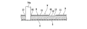
5 半導体基板
11 積層体
13 レーザ加工溝
15 歪(マイクロクラック)
17 切削溝
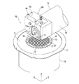
28 チャックテーブル
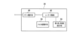
35 レーザビーム発生ユニット
37 集光器
78 切削ブレード
78a 切刃
W 半導体ウエーハ
D デバイス
Claims (3)
- 表面に低誘電率絶縁膜を含む積層体が積層され、該積層体によって格子状に交差する複数の分割予定ラインと該分割予定ラインで区画された各領域にデバイスが形成されたウエーハの加工方法であって、
該積層体に対して吸収性を有する波長のレーザビームを該分割予定ラインに沿って照射して、該積層体を分断するレーザ加工溝を形成するレーザ加工溝形成ステップと、
該レーザ加工溝形成ステップで形成されたレーザ加工溝に沿ってウエーハにレーザビームを照射して、該レーザ加工溝の底面に歪を形成する歪形成ステップと、
該歪形成ステップを実施した後、該レーザ加工溝に沿って切削ブレードでウエーハを切削する切削ステップと、
を具備したことを特徴とするウエーハの加工方法。 - 前記歪形成ステップで照射するレーザビームの波長は前記レーザ加工溝形成ステップで照射するレーザビームの波長と同一である請求項1記載のウエーハの加工方法。
- 前記歪形成ステップで照射するレーザビームの出力は前記レーザ加工溝形成ステップで照射するレーザビームの出力より大きい請求項1又は2記載のウエーハの加工方法。
Priority Applications (1)
| Application Number | Priority Date | Filing Date | Title |
|---|---|---|---|
| JP2011085634A JP5863264B2 (ja) | 2011-04-07 | 2011-04-07 | ウエーハの加工方法 |
Applications Claiming Priority (1)
| Application Number | Priority Date | Filing Date | Title |
|---|---|---|---|
| JP2011085634A JP5863264B2 (ja) | 2011-04-07 | 2011-04-07 | ウエーハの加工方法 |
Publications (2)
| Publication Number | Publication Date |
|---|---|
| JP2012222113A JP2012222113A (ja) | 2012-11-12 |
| JP5863264B2 true JP5863264B2 (ja) | 2016-02-16 |
Family
ID=47273318
Family Applications (1)
| Application Number | Title | Priority Date | Filing Date |
|---|---|---|---|
| JP2011085634A Active JP5863264B2 (ja) | 2011-04-07 | 2011-04-07 | ウエーハの加工方法 |
Country Status (1)
| Country | Link |
|---|---|
| JP (1) | JP5863264B2 (ja) |
Families Citing this family (2)
| Publication number | Priority date | Publication date | Assignee | Title |
|---|---|---|---|---|
| JP6305867B2 (ja) * | 2014-08-11 | 2018-04-04 | 株式会社ディスコ | ウエーハの加工方法 |
| CN116810187B (zh) * | 2023-08-31 | 2023-12-01 | 苏州天沐兴智能科技有限公司 | 一种晶圆激光切割方法、切割设备及可穿戴智能装置 |
Family Cites Families (8)
| Publication number | Priority date | Publication date | Assignee | Title |
|---|---|---|---|---|
| JP2003258182A (ja) * | 2002-02-28 | 2003-09-12 | Nippon Denkai Kk | 金属箔の粗化方法及び粗化金属箔 |
| WO2005034595A1 (ja) * | 2003-10-06 | 2005-04-14 | Shinko Electric Industries Co., Ltd. | 樹脂層へのビアホールの形成方法 |
| JP2006222258A (ja) * | 2005-02-10 | 2006-08-24 | Toshiba Corp | 半導体ウエハと半導体素子およびその製造方法 |
| JP2007173475A (ja) * | 2005-12-21 | 2007-07-05 | Disco Abrasive Syst Ltd | ウエーハの分割方法 |
| JP2007287780A (ja) * | 2006-04-13 | 2007-11-01 | Toshiba Corp | 半導体装置の製造方法及び半導体装置 |
| JP4959422B2 (ja) * | 2007-05-30 | 2012-06-20 | 株式会社ディスコ | ウエーハの分割方法 |
| JP2010021330A (ja) * | 2008-07-10 | 2010-01-28 | Disco Abrasive Syst Ltd | ウエーハの加工方法 |
| IL197349A0 (en) * | 2009-03-02 | 2009-12-24 | Orbotech Ltd | A method and system for electrical circuit repair |
-
2011
- 2011-04-07 JP JP2011085634A patent/JP5863264B2/ja active Active
Also Published As
| Publication number | Publication date |
|---|---|
| JP2012222113A (ja) | 2012-11-12 |
Similar Documents
| Publication | Publication Date | Title |
|---|---|---|
| JP4694845B2 (ja) | ウエーハの分割方法 | |
| KR102368338B1 (ko) | 웨이퍼의 가공 방법 | |
| KR102369760B1 (ko) | 웨이퍼의 가공 방법 | |
| JP4422463B2 (ja) | 半導体ウエーハの分割方法 | |
| CN105047612B (zh) | 晶片的加工方法 | |
| JP2009021476A (ja) | ウエーハの分割方法 | |
| JP2013197108A (ja) | ウエーハのレーザー加工方法 | |
| JP6178077B2 (ja) | ウエーハの加工方法 | |
| JP6815692B2 (ja) | ウェーハの加工方法 | |
| JP2006032419A (ja) | ウエーハのレーザー加工方法 | |
| JP2005209719A (ja) | 半導体ウエーハの加工方法 | |
| JP2008028113A (ja) | ウエーハのレーザー加工方法 | |
| US9087914B2 (en) | Wafer processing method | |
| JP2004179302A (ja) | 半導体ウエーハの分割方法 | |
| KR101893617B1 (ko) | 칩의 제조 방법 | |
| JP6257365B2 (ja) | ウェーハの加工方法 | |
| JP6837709B2 (ja) | デバイスウェーハのレーザ加工方法 | |
| JP2015167969A (ja) | レーザー加工装置及びレーザー加工方法 | |
| JP5453123B2 (ja) | 切削方法 | |
| JP5863264B2 (ja) | ウエーハの加工方法 | |
| JP6438304B2 (ja) | ウエーハの加工方法 | |
| JP6270520B2 (ja) | ウェーハの加工方法 | |
| JP2016162809A (ja) | ウエーハの加工方法 | |
| KR20150105210A (ko) | 판형물의 가공 방법 | |
| JP7463035B2 (ja) | 積層ウェーハの加工方法 |
Legal Events
| Date | Code | Title | Description |
|---|---|---|---|
| A621 | Written request for application examination |
Free format text: JAPANESE INTERMEDIATE CODE: A621 Effective date: 20140324 |
|
| A977 | Report on retrieval |
Free format text: JAPANESE INTERMEDIATE CODE: A971007 Effective date: 20150325 |
|
| A131 | Notification of reasons for refusal |
Free format text: JAPANESE INTERMEDIATE CODE: A131 Effective date: 20150331 |
|
| A521 | Request for written amendment filed |
Free format text: JAPANESE INTERMEDIATE CODE: A523 Effective date: 20150410 |
|
| TRDD | Decision of grant or rejection written | ||
| A01 | Written decision to grant a patent or to grant a registration (utility model) |
Free format text: JAPANESE INTERMEDIATE CODE: A01 Effective date: 20151222 |
|
| A61 | First payment of annual fees (during grant procedure) |
Free format text: JAPANESE INTERMEDIATE CODE: A61 Effective date: 20151222 |
|
| R150 | Certificate of patent or registration of utility model |
Ref document number: 5863264 Country of ref document: JP Free format text: JAPANESE INTERMEDIATE CODE: R150 |
|
| R250 | Receipt of annual fees |
Free format text: JAPANESE INTERMEDIATE CODE: R250 |
|
| R250 | Receipt of annual fees |
Free format text: JAPANESE INTERMEDIATE CODE: R250 |
|
| R250 | Receipt of annual fees |
Free format text: JAPANESE INTERMEDIATE CODE: R250 |
|
| R250 | Receipt of annual fees |
Free format text: JAPANESE INTERMEDIATE CODE: R250 |
|
| R250 | Receipt of annual fees |
Free format text: JAPANESE INTERMEDIATE CODE: R250 |
|
| R250 | Receipt of annual fees |
Free format text: JAPANESE INTERMEDIATE CODE: R250 |