JP5821991B2 - 半導体モジュール及び接合材料 - Google Patents
半導体モジュール及び接合材料 Download PDFInfo
- Publication number
- JP5821991B2 JP5821991B2 JP2014077543A JP2014077543A JP5821991B2 JP 5821991 B2 JP5821991 B2 JP 5821991B2 JP 2014077543 A JP2014077543 A JP 2014077543A JP 2014077543 A JP2014077543 A JP 2014077543A JP 5821991 B2 JP5821991 B2 JP 5821991B2
- Authority
- JP
- Japan
- Prior art keywords
- layer
- based layer
- bonding
- bonding material
- semiconductor module
- Prior art date
- Legal status (The legal status is an assumption and is not a legal conclusion. Google has not performed a legal analysis and makes no representation as to the accuracy of the status listed.)
- Expired - Fee Related
Links
Images


Classifications
-
- H—ELECTRICITY
- H01—ELECTRIC ELEMENTS
- H01L—SEMICONDUCTOR DEVICES NOT COVERED BY CLASS H10
- H01L2224/00—Indexing scheme for arrangements for connecting or disconnecting semiconductor or solid-state bodies and methods related thereto as covered by H01L24/00
- H01L2224/01—Means for bonding being attached to, or being formed on, the surface to be connected, e.g. chip-to-package, die-attach, "first-level" interconnects; Manufacturing methods related thereto
- H01L2224/26—Layer connectors, e.g. plate connectors, solder or adhesive layers; Manufacturing methods related thereto
- H01L2224/31—Structure, shape, material or disposition of the layer connectors after the connecting process
- H01L2224/32—Structure, shape, material or disposition of the layer connectors after the connecting process of an individual layer connector
- H01L2224/321—Disposition
- H01L2224/32151—Disposition the layer connector connecting between a semiconductor or solid-state body and an item not being a semiconductor or solid-state body, e.g. chip-to-substrate, chip-to-passive
- H01L2224/32221—Disposition the layer connector connecting between a semiconductor or solid-state body and an item not being a semiconductor or solid-state body, e.g. chip-to-substrate, chip-to-passive the body and the item being stacked
- H01L2224/32225—Disposition the layer connector connecting between a semiconductor or solid-state body and an item not being a semiconductor or solid-state body, e.g. chip-to-substrate, chip-to-passive the body and the item being stacked the item being non-metallic, e.g. insulating substrate with or without metallisation
-
- H—ELECTRICITY
- H01—ELECTRIC ELEMENTS
- H01L—SEMICONDUCTOR DEVICES NOT COVERED BY CLASS H10
- H01L2224/00—Indexing scheme for arrangements for connecting or disconnecting semiconductor or solid-state bodies and methods related thereto as covered by H01L24/00
- H01L2224/01—Means for bonding being attached to, or being formed on, the surface to be connected, e.g. chip-to-package, die-attach, "first-level" interconnects; Manufacturing methods related thereto
- H01L2224/26—Layer connectors, e.g. plate connectors, solder or adhesive layers; Manufacturing methods related thereto
- H01L2224/31—Structure, shape, material or disposition of the layer connectors after the connecting process
- H01L2224/32—Structure, shape, material or disposition of the layer connectors after the connecting process of an individual layer connector
- H01L2224/321—Disposition
- H01L2224/32151—Disposition the layer connector connecting between a semiconductor or solid-state body and an item not being a semiconductor or solid-state body, e.g. chip-to-substrate, chip-to-passive
- H01L2224/32221—Disposition the layer connector connecting between a semiconductor or solid-state body and an item not being a semiconductor or solid-state body, e.g. chip-to-substrate, chip-to-passive the body and the item being stacked
- H01L2224/32245—Disposition the layer connector connecting between a semiconductor or solid-state body and an item not being a semiconductor or solid-state body, e.g. chip-to-substrate, chip-to-passive the body and the item being stacked the item being metallic
-
- H—ELECTRICITY
- H01—ELECTRIC ELEMENTS
- H01L—SEMICONDUCTOR DEVICES NOT COVERED BY CLASS H10
- H01L2224/00—Indexing scheme for arrangements for connecting or disconnecting semiconductor or solid-state bodies and methods related thereto as covered by H01L24/00
- H01L2224/01—Means for bonding being attached to, or being formed on, the surface to be connected, e.g. chip-to-package, die-attach, "first-level" interconnects; Manufacturing methods related thereto
- H01L2224/42—Wire connectors; Manufacturing methods related thereto
- H01L2224/47—Structure, shape, material or disposition of the wire connectors after the connecting process
- H01L2224/48—Structure, shape, material or disposition of the wire connectors after the connecting process of an individual wire connector
- H01L2224/4805—Shape
- H01L2224/4809—Loop shape
- H01L2224/48091—Arched
-
- H—ELECTRICITY
- H01—ELECTRIC ELEMENTS
- H01L—SEMICONDUCTOR DEVICES NOT COVERED BY CLASS H10
- H01L2224/00—Indexing scheme for arrangements for connecting or disconnecting semiconductor or solid-state bodies and methods related thereto as covered by H01L24/00
- H01L2224/01—Means for bonding being attached to, or being formed on, the surface to be connected, e.g. chip-to-package, die-attach, "first-level" interconnects; Manufacturing methods related thereto
- H01L2224/42—Wire connectors; Manufacturing methods related thereto
- H01L2224/47—Structure, shape, material or disposition of the wire connectors after the connecting process
- H01L2224/48—Structure, shape, material or disposition of the wire connectors after the connecting process of an individual wire connector
- H01L2224/481—Disposition
- H01L2224/48135—Connecting between different semiconductor or solid-state bodies, i.e. chip-to-chip
- H01L2224/48137—Connecting between different semiconductor or solid-state bodies, i.e. chip-to-chip the bodies being arranged next to each other, e.g. on a common substrate
-
- H—ELECTRICITY
- H01—ELECTRIC ELEMENTS
- H01L—SEMICONDUCTOR DEVICES NOT COVERED BY CLASS H10
- H01L2224/00—Indexing scheme for arrangements for connecting or disconnecting semiconductor or solid-state bodies and methods related thereto as covered by H01L24/00
- H01L2224/01—Means for bonding being attached to, or being formed on, the surface to be connected, e.g. chip-to-package, die-attach, "first-level" interconnects; Manufacturing methods related thereto
- H01L2224/42—Wire connectors; Manufacturing methods related thereto
- H01L2224/47—Structure, shape, material or disposition of the wire connectors after the connecting process
- H01L2224/48—Structure, shape, material or disposition of the wire connectors after the connecting process of an individual wire connector
- H01L2224/481—Disposition
- H01L2224/48151—Connecting between a semiconductor or solid-state body and an item not being a semiconductor or solid-state body, e.g. chip-to-substrate, chip-to-passive
- H01L2224/48221—Connecting between a semiconductor or solid-state body and an item not being a semiconductor or solid-state body, e.g. chip-to-substrate, chip-to-passive the body and the item being stacked
- H01L2224/48225—Connecting between a semiconductor or solid-state body and an item not being a semiconductor or solid-state body, e.g. chip-to-substrate, chip-to-passive the body and the item being stacked the item being non-metallic, e.g. insulating substrate with or without metallisation
- H01L2224/48227—Connecting between a semiconductor or solid-state body and an item not being a semiconductor or solid-state body, e.g. chip-to-substrate, chip-to-passive the body and the item being stacked the item being non-metallic, e.g. insulating substrate with or without metallisation connecting the wire to a bond pad of the item
-
- H—ELECTRICITY
- H01—ELECTRIC ELEMENTS
- H01L—SEMICONDUCTOR DEVICES NOT COVERED BY CLASS H10
- H01L2224/00—Indexing scheme for arrangements for connecting or disconnecting semiconductor or solid-state bodies and methods related thereto as covered by H01L24/00
- H01L2224/01—Means for bonding being attached to, or being formed on, the surface to be connected, e.g. chip-to-package, die-attach, "first-level" interconnects; Manufacturing methods related thereto
- H01L2224/42—Wire connectors; Manufacturing methods related thereto
- H01L2224/47—Structure, shape, material or disposition of the wire connectors after the connecting process
- H01L2224/48—Structure, shape, material or disposition of the wire connectors after the connecting process of an individual wire connector
- H01L2224/481—Disposition
- H01L2224/48151—Connecting between a semiconductor or solid-state body and an item not being a semiconductor or solid-state body, e.g. chip-to-substrate, chip-to-passive
- H01L2224/48221—Connecting between a semiconductor or solid-state body and an item not being a semiconductor or solid-state body, e.g. chip-to-substrate, chip-to-passive the body and the item being stacked
- H01L2224/48245—Connecting between a semiconductor or solid-state body and an item not being a semiconductor or solid-state body, e.g. chip-to-substrate, chip-to-passive the body and the item being stacked the item being metallic
- H01L2224/48247—Connecting between a semiconductor or solid-state body and an item not being a semiconductor or solid-state body, e.g. chip-to-substrate, chip-to-passive the body and the item being stacked the item being metallic connecting the wire to a bond pad of the item
-
- H—ELECTRICITY
- H01—ELECTRIC ELEMENTS
- H01L—SEMICONDUCTOR DEVICES NOT COVERED BY CLASS H10
- H01L2224/00—Indexing scheme for arrangements for connecting or disconnecting semiconductor or solid-state bodies and methods related thereto as covered by H01L24/00
- H01L2224/73—Means for bonding being of different types provided for in two or more of groups H01L2224/10, H01L2224/18, H01L2224/26, H01L2224/34, H01L2224/42, H01L2224/50, H01L2224/63, H01L2224/71
- H01L2224/732—Location after the connecting process
- H01L2224/73251—Location after the connecting process on different surfaces
- H01L2224/73265—Layer and wire connectors
-
- H—ELECTRICITY
- H01—ELECTRIC ELEMENTS
- H01L—SEMICONDUCTOR DEVICES NOT COVERED BY CLASS H10
- H01L2924/00—Indexing scheme for arrangements or methods for connecting or disconnecting semiconductor or solid-state bodies as covered by H01L24/00
- H01L2924/10—Details of semiconductor or other solid state devices to be connected
- H01L2924/11—Device type
- H01L2924/13—Discrete devices, e.g. 3 terminal devices
- H01L2924/1304—Transistor
- H01L2924/1305—Bipolar Junction Transistor [BJT]
- H01L2924/13055—Insulated gate bipolar transistor [IGBT]
-
- H—ELECTRICITY
- H01—ELECTRIC ELEMENTS
- H01L—SEMICONDUCTOR DEVICES NOT COVERED BY CLASS H10
- H01L2924/00—Indexing scheme for arrangements or methods for connecting or disconnecting semiconductor or solid-state bodies as covered by H01L24/00
- H01L2924/10—Details of semiconductor or other solid state devices to be connected
- H01L2924/11—Device type
- H01L2924/13—Discrete devices, e.g. 3 terminal devices
- H01L2924/1304—Transistor
- H01L2924/1306—Field-effect transistor [FET]
- H01L2924/13091—Metal-Oxide-Semiconductor Field-Effect Transistor [MOSFET]
Description
また、X/Al/Zn積層材の間にZn系層を挟み、つまり、X/Al/Zn積層材、Zn系層、X/Al/Zn積層材を重ねてクラッド圧延することで、X/Al/Zn/Al/X積層材10を製造することができる。
さらには、第1のAl系層の片面にCu、Au、AgまたはSnのいずれかを主成分とする金属からなる第1のX系層を積層した第1のクラッド材の前記第1のAl系層側と、第2のAl系層の片面にCu、Au、AgまたはSnのいずれかを主成分とする金属からなる第2のX系層を積層した第2のクラッド材の前記第2のAl系層側とによってZn系層を挟持して、クラッド圧延することによって接合材料を形成することができる。
また、XがCuおよびAuの場合であって、X/Al/Zn/Al/Xの製造条件を適正化した場合、X層とAl層間にCu-Al金属間化合物、ないしAl-Au金属間化合物を生成させることができる。ここで、製造条件を適正化した場合とは、X層とAlの界面が加熱されるプロセスが存在する場合である。具体的には、X/Al/Zn/Al/Xを圧延で形成する場合は、X層とAl層との界面が加熱される。圧延率が大きいと、界面の温度上昇も大きい。圧延によって界面温度が200℃程度に上昇する場合は、上記金属間化合物が容易に形成される。一方、X層を蒸着やスパッタリングによって形成する場合は、界面の温度上昇は期待できず、金属間化合物の形成も生じない。
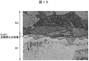
図15にXがCuの場合に、Cu/Al界面に形成されるCu-Al金属間化合物のTEM像を示す。このように、X/Al界面に10~300nm程度の厚さの金属間化合物を形成させることで、化合物層がXとAlの拡散バリアとして機能する。従って、化合物層がない場合より、高温・長時間の加熱でも、表面にAlが露出する現象を防止できる。また、Cu-Al化合物はZn-Alが溶融したときに、速やかにZn-Alに溶け込むため、接合を阻害しない。
さらに、XがSnの場合、加熱方法を変えることで、異なる接合構造を得ることが出来る。接合の模式図を図16に示す。図16(a)は、Sn/Al/Zn/Al/Sn積層材と被接合材を準備した状態を示す。この接合は、275〜365℃に1分以上保持することで行うが、図16の例では、300℃で接合する場合を示している。図16(b)は、Sn/Al/Zn/Al/Sn積層材を被接合材で挟み、温度上昇させ、230℃における状態を示す。この状態においては、Snが最初に溶け、隣接するAlもSn中に溶け始めた状態であり、Sn-Al共晶液相が形成された状態を示している。つまり、このとき、被接合材は、Al/Zn/Al層を挟んで、Sn-Al共晶液相で接合されている。さらに温度を上昇させ、300℃に加熱し、保持すると、ZnがAl層に拡散し、AlにZnが固溶したAl固溶体が形成される。このとき、AlはZnが50at.%程度固溶した固溶体となる。300℃に加熱された当初は、Al固溶体と被接合材の間にSn-Alの液相層が存在している。この状態が図16(c)である。さらに、300℃に保持すると、SnもZnもAlの固溶体となり、液相層は消失し、被接合材は固相である、Alの固溶体によって接合された状態となる。この状態が図16(d)である。その後、冷却すると、接合部材内、Sn固溶体、Al固溶体、Zn固溶体等が存在する状態となる。この状態が図16(e)である。図16は温度が300℃の場合の例であるが、275℃〜365℃の場合にも同様な現象が生ずる。
図17、図18にAl-Zn-Sn三元状態図を示す。Znの固溶量が少ないAl固溶体や、Zn固溶体にSnは殆ど固溶しないが、AlにZnが50at.%程度固溶したAl固溶体には、Snが30at.%程度固溶する特徴がある。図17、図18は各々280℃、290℃の状態を示しているが、このようなAl固溶体は275℃以上で生ずる。つまり、Znが50at.%程度固溶したAl固溶体層に、Sn-Al共晶液相のSnが拡散することで、Sn-Al液相が消失する。この時点で、被接合材は、ZnとSnが固溶したAl固溶体で接合される。なお、Zn層が相対的に分厚い場合は、接合層中央にZn層が残る場合もある。この後、全体を冷却すると、Al固溶体相は、Al固溶体、Zn固溶体、Sn固溶体にそれぞれ変化し、接合が完了する。
この接合方法では、前述のような、積層材全体を溶融させる接合方法よりも、最大100℃接合温度を下げることができ、半導体素子にかかる負荷を小さくできる。ただし、本接合法は275℃以上で可能であるが、実際の接合温度は290℃以上とした方が、Al固溶体層のSn固溶量が増加するため、接合時間を短時間化できる。また、接合層に析出する柔らかいSn固溶体が接合層の応力を緩和するため、接合信頼性が向上する。なお、本接合方法の場合は、Alを過不足なく固溶体化させるため、層厚比はAl:Zn:Al=5:1:5〜1:2:1の割合とすることが望ましい。
また、XがSnの場合、高湿度環境下における、SnによるZnの粒界腐食現象を防止するため、Mgを添加することが有効である。従って、AlやZnにMgを10wt.%を上限として添加したAl-Mg合金やZn-Mg合金を用いてもよい。また、Sn/Al/Zn/Al/Sn五層積層材ではなく、Sn/Al/Zn/Mg/Zn/Al/Sn七層積層材としてもよい。七層構造の場合、Mg層厚は総厚の1/10以下にすることが望ましい。これらの構造により、接合温度のさらなる低下、および耐食性の向上が可能である。Mgの添加量およびMg層厚が規定以上の場合、溶融後のZn-Al-Sn-Mg合金が脆弱化し、接合層の信頼性が低下することがある。
Invar Copper)、または、DBC(Direct Bond Copper)、DBA(Direct Bond Aluminum)などの金属を貼り合わせたセラミック基板(絶縁基板)など、どのような部材に対しても信頼性の高い接合を実現することができる。なお、Niメタライズの付いた被接合材を本発明の積層材で接合した場合の接合後の構造を詳細に書けば、被接合材/Ni/Ni-Al系化合物/Zn-Al-X合金/Ni-Al系化合物/Ni/被接合材となる。
また、本発明の積層材料は、板状構造に限定されるものではない。例えば、同心円状のワイヤー構造とすることができる。つまり、Znワイヤーを心材として、その外周にAl層、最外周にX系層を積層させることで、前述した板状の積層材と同様の耐酸化性能を発揮することが出来る。
[実施例1~24]
[実施例25]
[実施例26]
[実施例27]
[実施例28]
[実施例29]
[実施例30]
図11に記載の各種積層材のうち、No.2およびNo14の積層材と、No.2およびNo.14と同じ層構成で、Cu/Al界面およびAu/Al界面に金属間化合物層を生成させたNo.2’、No.14’材を用意した。全ての積層材を、融点直下の370℃で加熱保持した。その結果、表層のCuまたはAuが消失するまでの時間はNo.2は10min、No14は2min、No.2’は20min、No.14’は4minであった。何れも、実際の接合プロセスにおいては、十分な時間、表層が残存しており、耐酸化性は問題がない。金属間化合物を生成させたNo.2’、No.14’は、表層の残存時間が約2倍であり、極端に加熱速度が遅い場合にも、Zn、Alが酸化することなく接合することができる。また、No.2’、No.14’材を382℃以上に加熱し、積層材全体を溶融させた場合、界面の金属間化合物は、Zn-Al浴中に溶け込み、接合性を悪化させないことがわかった。
[実施例31]
図19に記載のSn/Al/Zn/Al/Sn積層材を用い、半導体素子とフレームを接合し、図1に示す半導体装置20を製造した。接合条件は、接合温度300℃、保持時間5min、荷重1kPa、N2雰囲気とした。その結果、接合温度がZn-Al共晶点以下であるが、Snが低温で溶融するため、接合可能であった。また、ボイド率10%以下の接合構造が実現できた。
[実施例32]
図11に記載の積層材をクラッド圧延により製造した。製造したクラッド材を1.0mm幅のリボン状に加工し、リールに巻きつけた。本リボン材料をダイボンダーに搭載し、リードフレームへの接合を実施した。具体的には、382℃以上に加熱したリードフレーム上に、リボン状のクラッド材を接触、溶融させ、Zn-Al-Xはんだをリードフレーム上に供給した。次いで、スパンクとよばれる、長方形の治具で溶融はんだを叩き広げるプロセスを経て、コレットによりはんだ上にチップを搭載した。チップ搭載時にはスクラブと呼ばれるチップを前後左右に振動させるプロセスを導入した。本プロセスでは雰囲気中の酸素濃度を100ppm以下とし、生成する微量のZn、Al酸化膜は、スパンクおよびスクラブプロセスにより除去することができた。従って、ボイド率は10%以下となり、良好な接合を得られた。一方、比較として、Zn-Al合金をリボン状に加工し、同様のプロセスで接合を試みた。しかし、Zn-Alの初期酸化膜が非常に強固なため、スパンクおよびスクラブのプロセスで、酸化膜を除去することが出来なかった。従って、接合部のボイド率が30%を超え、接合不良となった。
Claims (24)
- 半導体素子が接合材料を溶融した接合部を介して基板に接合している半導体モジュールであって、
前記接合材料は、Znを主成分として含有する金属からなるZn系層の第1の主面にAlを主成分として含有する金属からなる第1のAl系層と第1のX系層がこの順に積層された接合材料であって、前記第1のX系層は、Cu、Au、AgまたはSnのいずれかを主成分とする金属からなることを特徴とする半導体モジュール。 - 前記接合材料は、前記Zn系層の第1の主面とは反対側の第2の主面にAlを主成分として含有する金属からなる第2のAl系層と第2のX系層がこの順に積層されており、
前記第2のX系層は、Cu、Au、AgまたはSnのいずれかを主成分とする金属からなることを特徴とする請求項1に記載の半導体モジュール。 - 前記接合材料は、前記Zn系層の第1の主面とは反対側の第2の主面は、前記基板に接合されていることを特徴とする請求項1に記載の半導体モジュール。
- 前記接合材料は、前記第2のX系層の第2の主面は、前記基板に接合されていることを特徴とする請求項2に記載の半導体モジュール。
- 前記基板は、セラミック基板あるいは、被接合材である金属基板または金属フレームあるいは、金属キャップ、放熱用基板であることを特徴とする請求項1または3に記載の半導体モジュール。
- 前記基板は、セラミック基板あるいは、被接合材である金属基板または金属フレームあるいは、金属キャップ、放熱用基板であることを特徴とする請求項2または4に記載の半導体モジュール。
- 前記接合材料は、前記Zn系層は、Znを90〜100wt.%含有するZnを主成分とした単体層または合金層であることを特徴とする請求項1または3に記載の半導体モジュール。
- 前記接合材料は、前記Zn系層は、Znを90〜100wt.%含有するZnを主成分とした単体層または合金であることを特徴とする請求項2または4に記載の半導体モジュール。
- 前記接合材料は、前記第1または第2のAl系層は、Alを90〜100wt.%含有するAlを主成分とした単体層または合金層であることを特徴とする請求項2、4、6または8のいずれか1項に記載の半導体モジュール。
- 前記接合材料は、前記第1のAl系層は、Alを90〜100wt.%含有するAlを主成分とした単体層または合金層であることを特徴とする請求項1、3、5または7のいずれか1項に記載の半導体モジュール。
- 前記接合材料は、前記第1または第2のX系層は、Cuを90〜100wt.%含有するCuを主成分とした単体層または合金層であることを特徴とする請求項2、4、6または8のいずれか1項に記載の半導体モジュール。
- 前記接合材料は、前記第1のX系層は、Cuを90〜100wt.%含有するCuを主成分とした単体層または合金層であることを特徴とする請求項1、3、5または7のいずれか1項に記載の半導体モジュール。
- 前記接合材料は、前記第1または第2のX系層は、Auを90〜100wt.%含有するAuを主成分とした単体層または合金層であることを特徴とする請求項2、4、6または8のいずれか1項に記載の半導体モジュール。
- 前記接合材料は、前記第1のX系層は、Auを90〜100wt.%含有するAuを主成分とした単体層または合金層であることを特徴とする請求項1、3、5または7のいずれか1項に記載の半導体モジュール。
- 前記接合材料は、前記第1または第2のX系層は、Agを90〜100wt.%含有するAgを主成分とした単体層または合金層であることを特徴とする請求項2、4、6または8のいずれか1項に記載の半導体モジュール。
- 前記接合材料は、前記第1のX系層は、Agを90〜100wt.%含有するAgを主成分とした単体層または合金層であることを特徴とする請求項1、3、5または7のいずれか1項に記載の半導体モジュール。
- 前記接合材料は、前記第1または第2のX系層は、Snを90〜100wt.%含有するSnを主成分とした単体層または合金層であることを特徴とする請求項2、4、6または8のいずれか1項に記載の半導体モジュール。
- 前記接合材料は、前記第1または第2のX系層は、Snを90〜100wt.%含有するSnを主成分とした単体層または合金層であることを特徴とする請求項1、3、5または7のいずれか1項に記載の半導体モジュール。
- 前記接合材料は、(前記第1のX系層と前記第2のX系層の合計の膜厚)/(前記Zn系層と前記第1のAl系層と前記第2のAl系層の合計の膜厚)は、0.0002/1〜0.2/1であることを特徴とする請求項2、4、6、8、9、11、13、15、17のいずれか1項に記載の半導体モジュール。
- 前記接合材料は、(前記第1のAl系層と前記第2のAl系層の合計の膜厚)/(前記Zn系層の膜厚)は、1/60〜1/3であることを特徴とする請求項19に記載の半導体モジュール。
- 半導体素子が接合材料を溶融した接合部を介して基板に接合している半導体モジュールであって、
前記接合材料は、Znを主成分として含有する金属からなるZn系層の第1の主面にAlを主成分として含有する金属からなる第1のAl系層と第1のX系層がこの順に積層された接合材料であって、前記第1のX系層は、Cu、Au、AgまたはSnのいずれかを主成分とする金属からなり、
前記Zn系層の第1の主面とは反対側の第2の主面にMg合金層と前記Zn系層とは異なるZn系層とAlを主成分として含有する金属からなる第2のAl系層と第2のX系層がこの順に積層されており、
前記第2のX系層は、Snを主成分とする金属からなることを特徴とする半導体モジュール。 - 前記接合材料は、前記Mg合金層の層厚は積層された積層材の総厚の1/10以下であることを特徴とする請求項21に記載の半導体モジュール。
- Znを主成分として含有する金属からなるZn系層の第1の主面にAlを主成分として含有する金属からなる第1のAl系層と第1のX系層がこの順に積層された接合材料であって、前記第1のX系層は、Cu、Au、AgまたはSnのいずれかを主成分とする金属からなり、
前記Zn系層の第1の主面とは反対側の第2の主面にMg合金層と前記Zn系層とは異なるZn系層とAlを主成分として含有する金属からなる第2のAl系層と第2のX系層がこの順に積層されており、
前記第2のX系層は、Snを主成分とする金属からなることを特徴とする接合材料。 - 前記接合材料は、前記Mg合金層の層厚は積層された積層材の総厚の1/10以下であることを特徴とする請求項23に記載の接合材料。
Priority Applications (1)
| Application Number | Priority Date | Filing Date | Title |
|---|---|---|---|
| JP2014077543A JP5821991B2 (ja) | 2010-08-31 | 2014-04-04 | 半導体モジュール及び接合材料 |
Applications Claiming Priority (3)
| Application Number | Priority Date | Filing Date | Title |
|---|---|---|---|
| JP2010193885 | 2010-08-31 | ||
| JP2010193885 | 2010-08-31 | ||
| JP2014077543A JP5821991B2 (ja) | 2010-08-31 | 2014-04-04 | 半導体モジュール及び接合材料 |
Related Parent Applications (1)
| Application Number | Title | Priority Date | Filing Date |
|---|---|---|---|
| JP2011097178A Division JP5601275B2 (ja) | 2010-08-31 | 2011-04-25 | 接合材料、その製造方法、および接合構造の製造方法 |
Publications (2)
| Publication Number | Publication Date |
|---|---|
| JP2014170945A JP2014170945A (ja) | 2014-09-18 |
| JP5821991B2 true JP5821991B2 (ja) | 2015-11-24 |
Family
ID=51693074
Family Applications (1)
| Application Number | Title | Priority Date | Filing Date |
|---|---|---|---|
| JP2014077543A Expired - Fee Related JP5821991B2 (ja) | 2010-08-31 | 2014-04-04 | 半導体モジュール及び接合材料 |
Country Status (1)
| Country | Link |
|---|---|
| JP (1) | JP5821991B2 (ja) |
Families Citing this family (1)
| Publication number | Priority date | Publication date | Assignee | Title |
|---|---|---|---|---|
| CN112567504A (zh) * | 2018-11-30 | 2021-03-26 | 日立金属株式会社 | 电连接用部件、电连接结构和电连接用结构的制造方法 |
Family Cites Families (12)
| Publication number | Priority date | Publication date | Assignee | Title |
|---|---|---|---|---|
| US3167405A (en) * | 1957-05-08 | 1965-01-26 | Kaiser Aluminium Chem Corp | Laminated aluminum article |
| JPS5814311B2 (ja) * | 1976-04-23 | 1983-03-18 | 鳥羽工産株式会社 | 亜鉛合金とアルミニウムとの積層材並びにその製造法 |
| JPS5868941A (ja) * | 1981-10-21 | 1983-04-25 | Hitachi Ltd | ペレツトボンデイング方法 |
| JPH02121786A (ja) * | 1988-10-28 | 1990-05-09 | Sumitomo Chem Co Ltd | 銅・アルミニウムクラッド板の製造方法 |
| CN100578778C (zh) * | 2000-12-21 | 2010-01-06 | 株式会社日立制作所 | 电子器件 |
| US6815086B2 (en) * | 2001-11-21 | 2004-11-09 | Dana Canada Corporation | Methods for fluxless brazing |
| US7776454B2 (en) * | 2001-12-14 | 2010-08-17 | EMS Solutions, Inc. | Ti brazing strips or foils |
| JP4026747B2 (ja) * | 2002-04-12 | 2007-12-26 | アネスト岩田株式会社 | 圧縮部と膨張部を備えたスクロール式流体機械 |
| JP4961165B2 (ja) * | 2006-06-02 | 2012-06-27 | 日立協和エンジニアリング株式会社 | 電子部品搭載用基板、電子部品および電子装置 |
| JP4390799B2 (ja) * | 2006-11-21 | 2009-12-24 | 株式会社日立製作所 | 接続材料、接続材料の製造方法、および半導体装置 |
| JP4964009B2 (ja) * | 2007-04-17 | 2012-06-27 | 株式会社豊田中央研究所 | パワー半導体モジュール |
| JP4959539B2 (ja) * | 2007-12-18 | 2012-06-27 | 三菱電機株式会社 | 積層はんだ材およびそれを用いたはんだ付方法ならびにはんだ接合部 |
-
2014
- 2014-04-04 JP JP2014077543A patent/JP5821991B2/ja not_active Expired - Fee Related
Also Published As
| Publication number | Publication date |
|---|---|
| JP2014170945A (ja) | 2014-09-18 |
Similar Documents
| Publication | Publication Date | Title |
|---|---|---|
| JP5601275B2 (ja) | 接合材料、その製造方法、および接合構造の製造方法 | |
| EP1760783B1 (en) | Semiconductor device | |
| TWI284375B (en) | Semiconductor device and manufacturing method for semiconductor device | |
| JP5523680B2 (ja) | 接合体、半導体装置および接合体の製造方法 | |
| JP2010179336A (ja) | 接合体、半導体モジュール、及び接合体の製造方法 | |
| JP2004174522A (ja) | 複合はんだ、その製造方法および電子機器 | |
| JP5578326B2 (ja) | リード部品及びその製造方法、並びに半導体パッケージ | |
| JP2013176780A (ja) | 接合材料、その製造方法、および接合構造の製造方法 | |
| JP4959539B2 (ja) | 積層はんだ材およびそれを用いたはんだ付方法ならびにはんだ接合部 | |
| JP2005032834A (ja) | 半導体チップと基板との接合方法 | |
| JP2008221290A (ja) | 接合体および接合方法 | |
| JP2008080392A (ja) | 接合体および接合方法 | |
| JP5821991B2 (ja) | 半導体モジュール及び接合材料 | |
| JP2013146764A (ja) | 接続材料及びそれを用いたはんだ付け製品 | |
| JP5723225B2 (ja) | 接合構造体 | |
| JP6477517B2 (ja) | 半導体装置の製造方法 | |
| JP5533223B2 (ja) | 接合材料およびその製造方法、半導体装置およびその製造方法 | |
| JP5310309B2 (ja) | はんだコートリッド | |
| JP4745878B2 (ja) | はんだ皮膜及びそれを用いたはんだ付方法 | |
| JP2014184446A (ja) | 積層接合材料およびそれを用いて接合した接合体 | |
| KR102591963B1 (ko) | 금속 접합용 적층 구조체 및 금속 접합 방법 | |
| JP2012142320A (ja) | 半導体装置の製造方法 | |
| JP2007090404A (ja) | 接合体、半導体装置及び接合体の製造方法 | |
| JP2015160224A (ja) | 接合用材料 | |
| JP2015160237A (ja) | 接合材料及び半導体装置 |
Legal Events
| Date | Code | Title | Description |
|---|---|---|---|
| A977 | Report on retrieval |
Free format text: JAPANESE INTERMEDIATE CODE: A971007 Effective date: 20150220 |
|
| A131 | Notification of reasons for refusal |
Free format text: JAPANESE INTERMEDIATE CODE: A131 Effective date: 20150310 |
|
| A521 | Request for written amendment filed |
Free format text: JAPANESE INTERMEDIATE CODE: A523 Effective date: 20150507 |
|
| TRDD | Decision of grant or rejection written | ||
| A01 | Written decision to grant a patent or to grant a registration (utility model) |
Free format text: JAPANESE INTERMEDIATE CODE: A01 Effective date: 20150908 |
|
| A61 | First payment of annual fees (during grant procedure) |
Free format text: JAPANESE INTERMEDIATE CODE: A61 Effective date: 20150921 |
|
| R150 | Certificate of patent or registration of utility model |
Ref document number: 5821991 Country of ref document: JP Free format text: JAPANESE INTERMEDIATE CODE: R150 |
|
| LAPS | Cancellation because of no payment of annual fees |