JP5785496B2 - ファセットされたシリサイドコンタクトを有する半導体デバイス及び関連する製造方法 - Google Patents
ファセットされたシリサイドコンタクトを有する半導体デバイス及び関連する製造方法 Download PDFInfo
- Publication number
- JP5785496B2 JP5785496B2 JP2011531097A JP2011531097A JP5785496B2 JP 5785496 B2 JP5785496 B2 JP 5785496B2 JP 2011531097 A JP2011531097 A JP 2011531097A JP 2011531097 A JP2011531097 A JP 2011531097A JP 5785496 B2 JP5785496 B2 JP 5785496B2
- Authority
- JP
- Japan
- Prior art keywords
- semiconductor material
- recess
- semiconductor
- layer
- region
- Prior art date
- Legal status (The legal status is an assumption and is not a legal conclusion. Google has not performed a legal analysis and makes no representation as to the accuracy of the status listed.)
- Expired - Fee Related
Links
- 239000004065 semiconductor Substances 0.000 title claims description 190
- 238000004519 manufacturing process Methods 0.000 title claims description 46
- 229910021332 silicide Inorganic materials 0.000 title claims description 45
- FVBUAEGBCNSCDD-UHFFFAOYSA-N silicide(4-) Chemical compound [Si-4] FVBUAEGBCNSCDD-UHFFFAOYSA-N 0.000 title claims description 45
- 239000000463 material Substances 0.000 claims description 128
- 238000000034 method Methods 0.000 claims description 60
- 239000000945 filler Substances 0.000 claims description 34
- 239000000758 substrate Substances 0.000 claims description 19
- 238000005530 etching Methods 0.000 claims description 17
- 238000011065 in-situ storage Methods 0.000 claims description 8
- 229910000577 Silicon-germanium Inorganic materials 0.000 claims description 5
- LEVVHYCKPQWKOP-UHFFFAOYSA-N [Si].[Ge] Chemical compound [Si].[Ge] LEVVHYCKPQWKOP-UHFFFAOYSA-N 0.000 claims description 5
- 230000001939 inductive effect Effects 0.000 claims description 3
- 125000006850 spacer group Chemical group 0.000 description 31
- 239000012212 insulator Substances 0.000 description 26
- 230000015572 biosynthetic process Effects 0.000 description 18
- 238000005516 engineering process Methods 0.000 description 17
- 229910052751 metal Inorganic materials 0.000 description 15
- 239000002184 metal Substances 0.000 description 15
- 229910052710 silicon Inorganic materials 0.000 description 14
- 239000010703 silicon Substances 0.000 description 14
- XUIMIQQOPSSXEZ-UHFFFAOYSA-N Silicon Chemical compound [Si] XUIMIQQOPSSXEZ-UHFFFAOYSA-N 0.000 description 12
- 229910052581 Si3N4 Inorganic materials 0.000 description 9
- VYPSYNLAJGMNEJ-UHFFFAOYSA-N Silicium dioxide Chemical compound O=[Si]=O VYPSYNLAJGMNEJ-UHFFFAOYSA-N 0.000 description 9
- 239000007772 electrode material Substances 0.000 description 9
- HQVNEWCFYHHQES-UHFFFAOYSA-N silicon nitride Chemical compound N12[Si]34N5[Si]62N3[Si]51N64 HQVNEWCFYHHQES-UHFFFAOYSA-N 0.000 description 9
- 150000004767 nitrides Chemical class 0.000 description 8
- 229910021420 polycrystalline silicon Inorganic materials 0.000 description 8
- WGTYBPLFGIVFAS-UHFFFAOYSA-M tetramethylammonium hydroxide Chemical compound [OH-].C[N+](C)(C)C WGTYBPLFGIVFAS-UHFFFAOYSA-M 0.000 description 8
- KWYUFKZDYYNOTN-UHFFFAOYSA-M Potassium hydroxide Chemical compound [OH-].[K+] KWYUFKZDYYNOTN-UHFFFAOYSA-M 0.000 description 7
- 238000005229 chemical vapour deposition Methods 0.000 description 7
- 239000003989 dielectric material Substances 0.000 description 7
- 229910052814 silicon oxide Inorganic materials 0.000 description 7
- 239000000126 substance Substances 0.000 description 7
- 238000000231 atomic layer deposition Methods 0.000 description 5
- 238000004518 low pressure chemical vapour deposition Methods 0.000 description 5
- 238000001020 plasma etching Methods 0.000 description 5
- 238000000623 plasma-assisted chemical vapour deposition Methods 0.000 description 4
- 239000002210 silicon-based material Substances 0.000 description 4
- HMDDXIMCDZRSNE-UHFFFAOYSA-N [C].[Si] Chemical compound [C].[Si] HMDDXIMCDZRSNE-UHFFFAOYSA-N 0.000 description 3
- 238000000151 deposition Methods 0.000 description 3
- 230000001965 increasing effect Effects 0.000 description 3
- 238000005468 ion implantation Methods 0.000 description 3
- ZAMOUSCENKQFHK-UHFFFAOYSA-N Chlorine atom Chemical compound [Cl] ZAMOUSCENKQFHK-UHFFFAOYSA-N 0.000 description 2
- PXHVJJICTQNCMI-UHFFFAOYSA-N Nickel Chemical compound [Ni] PXHVJJICTQNCMI-UHFFFAOYSA-N 0.000 description 2
- KDLHZDBZIXYQEI-UHFFFAOYSA-N Palladium Chemical compound [Pd] KDLHZDBZIXYQEI-UHFFFAOYSA-N 0.000 description 2
- NBIIXXVUZAFLBC-UHFFFAOYSA-N Phosphoric acid Chemical compound OP(O)(O)=O NBIIXXVUZAFLBC-UHFFFAOYSA-N 0.000 description 2
- 239000000460 chlorine Substances 0.000 description 2
- 229910052801 chlorine Inorganic materials 0.000 description 2
- 239000004020 conductor Substances 0.000 description 2
- 239000013078 crystal Substances 0.000 description 2
- 230000005669 field effect Effects 0.000 description 2
- 229910052732 germanium Inorganic materials 0.000 description 2
- GNPVGFCGXDBREM-UHFFFAOYSA-N germanium atom Chemical compound [Ge] GNPVGFCGXDBREM-UHFFFAOYSA-N 0.000 description 2
- 238000002513 implantation Methods 0.000 description 2
- 239000007769 metal material Substances 0.000 description 2
- 238000001039 wet etching Methods 0.000 description 2
- JBRZTFJDHDCESZ-UHFFFAOYSA-N AsGa Chemical compound [As]#[Ga] JBRZTFJDHDCESZ-UHFFFAOYSA-N 0.000 description 1
- ZOXJGFHDIHLPTG-UHFFFAOYSA-N Boron Chemical compound [B] ZOXJGFHDIHLPTG-UHFFFAOYSA-N 0.000 description 1
- OKTJSMMVPCPJKN-UHFFFAOYSA-N Carbon Chemical compound [C] OKTJSMMVPCPJKN-UHFFFAOYSA-N 0.000 description 1
- 229910001218 Gallium arsenide Inorganic materials 0.000 description 1
- 229910004129 HfSiO Inorganic materials 0.000 description 1
- UFHFLCQGNIYNRP-UHFFFAOYSA-N Hydrogen Chemical compound [H][H] UFHFLCQGNIYNRP-UHFFFAOYSA-N 0.000 description 1
- KJTLSVCANCCWHF-UHFFFAOYSA-N Ruthenium Chemical compound [Ru] KJTLSVCANCCWHF-UHFFFAOYSA-N 0.000 description 1
- BLRPTPMANUNPDV-UHFFFAOYSA-N Silane Chemical compound [SiH4] BLRPTPMANUNPDV-UHFFFAOYSA-N 0.000 description 1
- 229910045601 alloy Inorganic materials 0.000 description 1
- 239000000956 alloy Substances 0.000 description 1
- 229910000147 aluminium phosphate Inorganic materials 0.000 description 1
- 230000003466 anti-cipated effect Effects 0.000 description 1
- 238000013459 approach Methods 0.000 description 1
- 229910052796 boron Inorganic materials 0.000 description 1
- 229910052799 carbon Inorganic materials 0.000 description 1
- 229910017052 cobalt Inorganic materials 0.000 description 1
- 239000010941 cobalt Substances 0.000 description 1
- GUTLYIVDDKVIGB-UHFFFAOYSA-N cobalt atom Chemical compound [Co] GUTLYIVDDKVIGB-UHFFFAOYSA-N 0.000 description 1
- 230000000295 complement effect Effects 0.000 description 1
- 238000007796 conventional method Methods 0.000 description 1
- 230000007423 decrease Effects 0.000 description 1
- 230000008021 deposition Effects 0.000 description 1
- 238000013461 design Methods 0.000 description 1
- 238000011161 development Methods 0.000 description 1
- 239000002019 doping agent Substances 0.000 description 1
- 238000010438 heat treatment Methods 0.000 description 1
- BHEPBYXIRTUNPN-UHFFFAOYSA-N hydridophosphorus(.) (triplet) Chemical compound [PH] BHEPBYXIRTUNPN-UHFFFAOYSA-N 0.000 description 1
- 229910052739 hydrogen Inorganic materials 0.000 description 1
- 239000001257 hydrogen Substances 0.000 description 1
- 239000012535 impurity Substances 0.000 description 1
- 239000011810 insulating material Substances 0.000 description 1
- 238000009413 insulation Methods 0.000 description 1
- 229910044991 metal oxide Inorganic materials 0.000 description 1
- 150000004706 metal oxides Chemical class 0.000 description 1
- 229910052759 nickel Inorganic materials 0.000 description 1
- 238000004806 packaging method and process Methods 0.000 description 1
- 229910052763 palladium Inorganic materials 0.000 description 1
- 238000005498 polishing Methods 0.000 description 1
- 238000004151 rapid thermal annealing Methods 0.000 description 1
- 229910052702 rhenium Inorganic materials 0.000 description 1
- WUAPFZMCVAUBPE-UHFFFAOYSA-N rhenium atom Chemical compound [Re] WUAPFZMCVAUBPE-UHFFFAOYSA-N 0.000 description 1
- 229910052707 ruthenium Inorganic materials 0.000 description 1
- 229910000077 silane Inorganic materials 0.000 description 1
- 239000000377 silicon dioxide Substances 0.000 description 1
- 235000012239 silicon dioxide Nutrition 0.000 description 1
- 238000004544 sputter deposition Methods 0.000 description 1
- WFKWXMTUELFFGS-UHFFFAOYSA-N tungsten Chemical compound [W] WFKWXMTUELFFGS-UHFFFAOYSA-N 0.000 description 1
- 229910052721 tungsten Inorganic materials 0.000 description 1
- 239000010937 tungsten Substances 0.000 description 1
Images


Classifications
-
- H—ELECTRICITY
- H01—ELECTRIC ELEMENTS
- H01L—SEMICONDUCTOR DEVICES NOT COVERED BY CLASS H10
- H01L29/00—Semiconductor devices adapted for rectifying, amplifying, oscillating or switching, or capacitors or resistors with at least one potential-jump barrier or surface barrier, e.g. PN junction depletion layer or carrier concentration layer; Details of semiconductor bodies or of electrodes thereof ; Multistep manufacturing processes therefor
- H01L29/66—Types of semiconductor device ; Multistep manufacturing processes therefor
- H01L29/66007—Multistep manufacturing processes
- H01L29/66075—Multistep manufacturing processes of devices having semiconductor bodies comprising group 14 or group 13/15 materials
- H01L29/66227—Multistep manufacturing processes of devices having semiconductor bodies comprising group 14 or group 13/15 materials the devices being controllable only by the electric current supplied or the electric potential applied, to an electrode which does not carry the current to be rectified, amplified or switched, e.g. three-terminal devices
- H01L29/66409—Unipolar field-effect transistors
- H01L29/66477—Unipolar field-effect transistors with an insulated gate, i.e. MISFET
- H01L29/66568—Lateral single gate silicon transistors
- H01L29/66636—Lateral single gate silicon transistors with source or drain recessed by etching or first recessed by etching and then refilled
-
- H—ELECTRICITY
- H01—ELECTRIC ELEMENTS
- H01L—SEMICONDUCTOR DEVICES NOT COVERED BY CLASS H10
- H01L21/00—Processes or apparatus adapted for the manufacture or treatment of semiconductor or solid state devices or of parts thereof
- H01L21/02—Manufacture or treatment of semiconductor devices or of parts thereof
- H01L21/02104—Forming layers
- H01L21/02365—Forming inorganic semiconducting materials on a substrate
- H01L21/02367—Substrates
- H01L21/0237—Materials
- H01L21/02373—Group 14 semiconducting materials
- H01L21/02381—Silicon, silicon germanium, germanium
-
- H—ELECTRICITY
- H01—ELECTRIC ELEMENTS
- H01L—SEMICONDUCTOR DEVICES NOT COVERED BY CLASS H10
- H01L21/00—Processes or apparatus adapted for the manufacture or treatment of semiconductor or solid state devices or of parts thereof
- H01L21/02—Manufacture or treatment of semiconductor devices or of parts thereof
- H01L21/02104—Forming layers
- H01L21/02365—Forming inorganic semiconducting materials on a substrate
- H01L21/02367—Substrates
- H01L21/02433—Crystal orientation
-
- H—ELECTRICITY
- H01—ELECTRIC ELEMENTS
- H01L—SEMICONDUCTOR DEVICES NOT COVERED BY CLASS H10
- H01L21/00—Processes or apparatus adapted for the manufacture or treatment of semiconductor or solid state devices or of parts thereof
- H01L21/02—Manufacture or treatment of semiconductor devices or of parts thereof
- H01L21/02104—Forming layers
- H01L21/02365—Forming inorganic semiconducting materials on a substrate
- H01L21/02518—Deposited layers
- H01L21/02521—Materials
- H01L21/02524—Group 14 semiconducting materials
- H01L21/02529—Silicon carbide
-
- H—ELECTRICITY
- H01—ELECTRIC ELEMENTS
- H01L—SEMICONDUCTOR DEVICES NOT COVERED BY CLASS H10
- H01L21/00—Processes or apparatus adapted for the manufacture or treatment of semiconductor or solid state devices or of parts thereof
- H01L21/02—Manufacture or treatment of semiconductor devices or of parts thereof
- H01L21/02104—Forming layers
- H01L21/02365—Forming inorganic semiconducting materials on a substrate
- H01L21/02518—Deposited layers
- H01L21/02521—Materials
- H01L21/02524—Group 14 semiconducting materials
- H01L21/02532—Silicon, silicon germanium, germanium
-
- H—ELECTRICITY
- H01—ELECTRIC ELEMENTS
- H01L—SEMICONDUCTOR DEVICES NOT COVERED BY CLASS H10
- H01L21/00—Processes or apparatus adapted for the manufacture or treatment of semiconductor or solid state devices or of parts thereof
- H01L21/02—Manufacture or treatment of semiconductor devices or of parts thereof
- H01L21/02104—Forming layers
- H01L21/02365—Forming inorganic semiconducting materials on a substrate
- H01L21/02518—Deposited layers
- H01L21/02609—Crystal orientation
-
- H—ELECTRICITY
- H01—ELECTRIC ELEMENTS
- H01L—SEMICONDUCTOR DEVICES NOT COVERED BY CLASS H10
- H01L21/00—Processes or apparatus adapted for the manufacture or treatment of semiconductor or solid state devices or of parts thereof
- H01L21/02—Manufacture or treatment of semiconductor devices or of parts thereof
- H01L21/02104—Forming layers
- H01L21/02365—Forming inorganic semiconducting materials on a substrate
- H01L21/02612—Formation types
- H01L21/02617—Deposition types
- H01L21/02636—Selective deposition, e.g. simultaneous growth of mono- and non-monocrystalline semiconductor materials
-
- H—ELECTRICITY
- H01—ELECTRIC ELEMENTS
- H01L—SEMICONDUCTOR DEVICES NOT COVERED BY CLASS H10
- H01L29/00—Semiconductor devices adapted for rectifying, amplifying, oscillating or switching, or capacitors or resistors with at least one potential-jump barrier or surface barrier, e.g. PN junction depletion layer or carrier concentration layer; Details of semiconductor bodies or of electrodes thereof ; Multistep manufacturing processes therefor
- H01L29/02—Semiconductor bodies ; Multistep manufacturing processes therefor
- H01L29/04—Semiconductor bodies ; Multistep manufacturing processes therefor characterised by their crystalline structure, e.g. polycrystalline, cubic or particular orientation of crystalline planes
- H01L29/045—Semiconductor bodies ; Multistep manufacturing processes therefor characterised by their crystalline structure, e.g. polycrystalline, cubic or particular orientation of crystalline planes by their particular orientation of crystalline planes
-
- H—ELECTRICITY
- H01—ELECTRIC ELEMENTS
- H01L—SEMICONDUCTOR DEVICES NOT COVERED BY CLASS H10
- H01L29/00—Semiconductor devices adapted for rectifying, amplifying, oscillating or switching, or capacitors or resistors with at least one potential-jump barrier or surface barrier, e.g. PN junction depletion layer or carrier concentration layer; Details of semiconductor bodies or of electrodes thereof ; Multistep manufacturing processes therefor
- H01L29/40—Electrodes ; Multistep manufacturing processes therefor
- H01L29/41—Electrodes ; Multistep manufacturing processes therefor characterised by their shape, relative sizes or dispositions
- H01L29/417—Electrodes ; Multistep manufacturing processes therefor characterised by their shape, relative sizes or dispositions carrying the current to be rectified, amplified or switched
- H01L29/41725—Source or drain electrodes for field effect devices
- H01L29/41766—Source or drain electrodes for field effect devices with at least part of the source or drain electrode having contact below the semiconductor surface, e.g. the source or drain electrode formed at least partially in a groove or with inclusions of conductor inside the semiconductor
-
- H—ELECTRICITY
- H01—ELECTRIC ELEMENTS
- H01L—SEMICONDUCTOR DEVICES NOT COVERED BY CLASS H10
- H01L29/00—Semiconductor devices adapted for rectifying, amplifying, oscillating or switching, or capacitors or resistors with at least one potential-jump barrier or surface barrier, e.g. PN junction depletion layer or carrier concentration layer; Details of semiconductor bodies or of electrodes thereof ; Multistep manufacturing processes therefor
- H01L29/66—Types of semiconductor device ; Multistep manufacturing processes therefor
- H01L29/66007—Multistep manufacturing processes
- H01L29/66075—Multistep manufacturing processes of devices having semiconductor bodies comprising group 14 or group 13/15 materials
- H01L29/66227—Multistep manufacturing processes of devices having semiconductor bodies comprising group 14 or group 13/15 materials the devices being controllable only by the electric current supplied or the electric potential applied, to an electrode which does not carry the current to be rectified, amplified or switched, e.g. three-terminal devices
- H01L29/66409—Unipolar field-effect transistors
- H01L29/66477—Unipolar field-effect transistors with an insulated gate, i.e. MISFET
- H01L29/66568—Lateral single gate silicon transistors
- H01L29/66613—Lateral single gate silicon transistors with a gate recessing step, e.g. using local oxidation
- H01L29/66628—Lateral single gate silicon transistors with a gate recessing step, e.g. using local oxidation recessing the gate by forming single crystalline semiconductor material at the source or drain location
-
- H—ELECTRICITY
- H01—ELECTRIC ELEMENTS
- H01L—SEMICONDUCTOR DEVICES NOT COVERED BY CLASS H10
- H01L29/00—Semiconductor devices adapted for rectifying, amplifying, oscillating or switching, or capacitors or resistors with at least one potential-jump barrier or surface barrier, e.g. PN junction depletion layer or carrier concentration layer; Details of semiconductor bodies or of electrodes thereof ; Multistep manufacturing processes therefor
- H01L29/66—Types of semiconductor device ; Multistep manufacturing processes therefor
- H01L29/68—Types of semiconductor device ; Multistep manufacturing processes therefor controllable by only the electric current supplied, or only the electric potential applied, to an electrode which does not carry the current to be rectified, amplified or switched
- H01L29/76—Unipolar devices, e.g. field effect transistors
- H01L29/772—Field effect transistors
- H01L29/78—Field effect transistors with field effect produced by an insulated gate
- H01L29/7842—Field effect transistors with field effect produced by an insulated gate means for exerting mechanical stress on the crystal lattice of the channel region, e.g. using a flexible substrate
- H01L29/7848—Field effect transistors with field effect produced by an insulated gate means for exerting mechanical stress on the crystal lattice of the channel region, e.g. using a flexible substrate the means being located in the source/drain region, e.g. SiGe source and drain
-
- H—ELECTRICITY
- H01—ELECTRIC ELEMENTS
- H01L—SEMICONDUCTOR DEVICES NOT COVERED BY CLASS H10
- H01L29/00—Semiconductor devices adapted for rectifying, amplifying, oscillating or switching, or capacitors or resistors with at least one potential-jump barrier or surface barrier, e.g. PN junction depletion layer or carrier concentration layer; Details of semiconductor bodies or of electrodes thereof ; Multistep manufacturing processes therefor
- H01L29/66—Types of semiconductor device ; Multistep manufacturing processes therefor
- H01L29/66007—Multistep manufacturing processes
- H01L29/66075—Multistep manufacturing processes of devices having semiconductor bodies comprising group 14 or group 13/15 materials
- H01L29/66227—Multistep manufacturing processes of devices having semiconductor bodies comprising group 14 or group 13/15 materials the devices being controllable only by the electric current supplied or the electric potential applied, to an electrode which does not carry the current to be rectified, amplified or switched, e.g. three-terminal devices
- H01L29/66409—Unipolar field-effect transistors
- H01L29/66477—Unipolar field-effect transistors with an insulated gate, i.e. MISFET
- H01L29/665—Unipolar field-effect transistors with an insulated gate, i.e. MISFET using self aligned silicidation, i.e. salicide
-
- H—ELECTRICITY
- H01—ELECTRIC ELEMENTS
- H01L—SEMICONDUCTOR DEVICES NOT COVERED BY CLASS H10
- H01L29/00—Semiconductor devices adapted for rectifying, amplifying, oscillating or switching, or capacitors or resistors with at least one potential-jump barrier or surface barrier, e.g. PN junction depletion layer or carrier concentration layer; Details of semiconductor bodies or of electrodes thereof ; Multistep manufacturing processes therefor
- H01L29/66—Types of semiconductor device ; Multistep manufacturing processes therefor
- H01L29/66007—Multistep manufacturing processes
- H01L29/66075—Multistep manufacturing processes of devices having semiconductor bodies comprising group 14 or group 13/15 materials
- H01L29/66227—Multistep manufacturing processes of devices having semiconductor bodies comprising group 14 or group 13/15 materials the devices being controllable only by the electric current supplied or the electric potential applied, to an electrode which does not carry the current to be rectified, amplified or switched, e.g. three-terminal devices
- H01L29/66409—Unipolar field-effect transistors
- H01L29/66477—Unipolar field-effect transistors with an insulated gate, i.e. MISFET
- H01L29/6653—Unipolar field-effect transistors with an insulated gate, i.e. MISFET using the removal of at least part of spacer, e.g. disposable spacer
-
- H—ELECTRICITY
- H01—ELECTRIC ELEMENTS
- H01L—SEMICONDUCTOR DEVICES NOT COVERED BY CLASS H10
- H01L29/00—Semiconductor devices adapted for rectifying, amplifying, oscillating or switching, or capacitors or resistors with at least one potential-jump barrier or surface barrier, e.g. PN junction depletion layer or carrier concentration layer; Details of semiconductor bodies or of electrodes thereof ; Multistep manufacturing processes therefor
- H01L29/66—Types of semiconductor device ; Multistep manufacturing processes therefor
- H01L29/66007—Multistep manufacturing processes
- H01L29/66075—Multistep manufacturing processes of devices having semiconductor bodies comprising group 14 or group 13/15 materials
- H01L29/66227—Multistep manufacturing processes of devices having semiconductor bodies comprising group 14 or group 13/15 materials the devices being controllable only by the electric current supplied or the electric potential applied, to an electrode which does not carry the current to be rectified, amplified or switched, e.g. three-terminal devices
- H01L29/66409—Unipolar field-effect transistors
- H01L29/66477—Unipolar field-effect transistors with an insulated gate, i.e. MISFET
- H01L29/66545—Unipolar field-effect transistors with an insulated gate, i.e. MISFET using a dummy, i.e. replacement gate in a process wherein at least a part of the final gate is self aligned to the dummy gate
-
- H—ELECTRICITY
- H01—ELECTRIC ELEMENTS
- H01L—SEMICONDUCTOR DEVICES NOT COVERED BY CLASS H10
- H01L29/00—Semiconductor devices adapted for rectifying, amplifying, oscillating or switching, or capacitors or resistors with at least one potential-jump barrier or surface barrier, e.g. PN junction depletion layer or carrier concentration layer; Details of semiconductor bodies or of electrodes thereof ; Multistep manufacturing processes therefor
- H01L29/66—Types of semiconductor device ; Multistep manufacturing processes therefor
- H01L29/66007—Multistep manufacturing processes
- H01L29/66075—Multistep manufacturing processes of devices having semiconductor bodies comprising group 14 or group 13/15 materials
- H01L29/66227—Multistep manufacturing processes of devices having semiconductor bodies comprising group 14 or group 13/15 materials the devices being controllable only by the electric current supplied or the electric potential applied, to an electrode which does not carry the current to be rectified, amplified or switched, e.g. three-terminal devices
- H01L29/66409—Unipolar field-effect transistors
- H01L29/66477—Unipolar field-effect transistors with an insulated gate, i.e. MISFET
- H01L29/6656—Unipolar field-effect transistors with an insulated gate, i.e. MISFET using multiple spacer layers, e.g. multiple sidewall spacers
Landscapes
- Engineering & Computer Science (AREA)
- Microelectronics & Electronic Packaging (AREA)
- Power Engineering (AREA)
- Computer Hardware Design (AREA)
- Condensed Matter Physics & Semiconductors (AREA)
- General Physics & Mathematics (AREA)
- Physics & Mathematics (AREA)
- Manufacturing & Machinery (AREA)
- Chemical & Material Sciences (AREA)
- Ceramic Engineering (AREA)
- Crystallography & Structural Chemistry (AREA)
- Materials Engineering (AREA)
- Insulated Gate Type Field-Effect Transistor (AREA)
- Electrodes Of Semiconductors (AREA)
- Recrystallisation Techniques (AREA)
- Metal-Oxide And Bipolar Metal-Oxide Semiconductor Integrated Circuits (AREA)
Description
Claims (9)
- 半導体デバイス(300)を製造する方法であって、
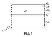
半導体材質(102)の層を有する基板(100)を提供することと、
半導体材質(102)の前記層を覆うゲート構造(112,128)を作製することと、
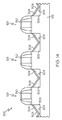
前記ゲート構造(112,128)に隣接する半導体材質(102)の前記層内に凹部(202)を形成して、前記半導体材質(102)の{110}面に一致する露出させられた凹部表面(204)をもたらすために、前記半導体材質(102)の一部を異方性エッチングすることと、
摂氏500〜580度の範囲内の成長温度の下で前記凹部(202)内のフィラー半導体材質(302)をエピタキシャル成長させることによって、前記凹部(202)を少なくとも部分的に充填して、前記凹部(202)内にファセット形状半導体領域(304)を形成することとを備え、
前記ファセット形状半導体領域(304)は、2つの{111}面の交差において、前記基板(100)に対して下を向き、前記露出させられた凹部表面(204)を向いているファセット領域(306)を備えている、方法。 - 前記凹部(202)を少なくとも部分的に充填することは、前記凹部内にその場でドープされる半導体材質(302)をエピタキシャル成長させることを備えている請求項1の方法。
- 前記凹部(202)を少なくとも部分的に充填した後に前記ファセット形状半導体領域(304)上にシリサイドコンタクト区域(308)を形成することを更に備えた請求項1の方法。
- 前記凹部(202)を少なくとも部分的に充填することは、応力誘起半導体材質(302)で前記凹部(202)を少なくとも部分的に充填することを備えている請求項1の方法。
- 半導体デバイス(200)であって、
半導体材質(102)の層と、
半導体材質(102)の前記層を覆うゲート構造(112,128)と、
半導体材質(102)の前記層内のチャネル領域(218)であって前記ゲート構造(112,128)の下層となるチャネル領域(218)と、
半導体材質(102)の前記層内のソース及びドレイン領域(216)であって、前記チャネル領域(218)がそれらの間に配置され、ファセット形状半導体領域(206,306)を備えたソース及びドレイン領域(216)と、
前記ソース及びドレイン領域(216)を覆うファセット形状シリサイドコンタクト区域(210,308,406)と、
前記ゲート構造(112,128)に隣接する前記半導体材質(102)の前記層に形成された凹部(202)であって、前記半導体材質(102)の{110}面に一致する凹部表面(204)を有する凹部(202)内に配置されたファセット形状半導体領域(206,306)であって、表面に前記ファセット形状シリサイドコンタクト区域(210,308)が形成されているファセット形状半導体領域(206,306)と、を備え、
前記半導体デバイス(200)はPMOSトランジスタデバイスであって、
前記半導体材質(102)の前記層はシリコンゲルマニウムであって、
前記ファセット形状半導体領域は前記シリコンゲルマニウムの2つの{111}面の交差によって部分的に画定されており、
前記ファセット形状半導体領域(206,306)が、2つの{111}面の交差において、前記基板(100)に対して下を向き、前記凹部表面(204)を向いている下向きファセット領域(306)か、2つの{111}面の交差に頂を有し、前記基板(100)に対して上を向き、前記凹部表面(204)の逆を向いている上向きファセット領域(206)のいずれかを備えている、半導体デバイス(200,300,400)。 - 半導体デバイス(200)を製造する方法であって、
半導体材質(102)の層を有する基板(100)を提供することと、
前記半導体材質(102)の前記層を覆うゲート構造(112,128)を作製することと、
前記ゲート構造(112,128)に隣接する半導体材質(102)の前記層内に凹部(202)を形成して、前記半導体材質(102)の{110}面に一致する露出させられた凹部表面(204)をもたらすために、前記半導体材質(102)の一部を異方性エッチングすることと、
摂氏600〜650度の範囲内の成長温度の下で前記凹部(202)内のフィラー半導体材質(205)をエピタキシャル成長させることによって、前記凹部(202)を少なくとも部分的に充填して、前記凹部(202)内にファセット形状半導体領域(206)を形成することとを備え、
前記ファセット形状半導体領域(206)は、2つの{111}面の交差に頂を有し、前記基板(100)に対して上を向き、前記露出させられた凹部表面(204)の逆を向いている上向きファセット領域(208)を備えている、方法。 - 前記凹部(202)を少なくとも部分的に充填することは、前記凹部内にその場でドープされる半導体材質(302)をエピタキシャル成長させることを備えている請求項6の方法。
- 前記凹部(202)を少なくとも部分的に充填した後に前記ファセット形状半導体領域(206)上にシリサイドコンタクト区域(210,308)を形成することを更に備えた請求項6の方法。
- 前記凹部(202)を少なくとも部分的に充填することは、応力誘起半導体材質(205)で前記凹部(202)を少なくとも部分的に充填することを備えている請求項6の方法。
Applications Claiming Priority (3)
| Application Number | Priority Date | Filing Date | Title |
|---|---|---|---|
| US12/249,570 | 2008-10-10 | ||
| US12/249,570 US7994014B2 (en) | 2008-10-10 | 2008-10-10 | Semiconductor devices having faceted silicide contacts, and related fabrication methods |
| PCT/US2009/059560 WO2010051133A2 (en) | 2008-10-10 | 2009-10-05 | Semiconductor devices having faceted silicide contacts, and related fabrication methods |
Publications (3)
| Publication Number | Publication Date |
|---|---|
| JP2012505547A JP2012505547A (ja) | 2012-03-01 |
| JP2012505547A5 JP2012505547A5 (ja) | 2012-11-22 |
| JP5785496B2 true JP5785496B2 (ja) | 2015-09-30 |
Family
ID=42062020
Family Applications (1)
| Application Number | Title | Priority Date | Filing Date |
|---|---|---|---|
| JP2011531097A Expired - Fee Related JP5785496B2 (ja) | 2008-10-10 | 2009-10-05 | ファセットされたシリサイドコンタクトを有する半導体デバイス及び関連する製造方法 |
Country Status (6)
| Country | Link |
|---|---|
| US (1) | US7994014B2 (ja) |
| EP (1) | EP2345065A2 (ja) |
| JP (1) | JP5785496B2 (ja) |
| KR (1) | KR101639771B1 (ja) |
| CN (1) | CN102177573B (ja) |
| WO (1) | WO2010051133A2 (ja) |
Families Citing this family (22)
| Publication number | Priority date | Publication date | Assignee | Title |
|---|---|---|---|---|
| US7445978B2 (en) * | 2005-05-04 | 2008-11-04 | Chartered Semiconductor Manufacturing, Ltd | Method to remove spacer after salicidation to enhance contact etch stop liner stress on MOS |
| DE102009031114B4 (de) * | 2009-06-30 | 2011-07-07 | Globalfoundries Dresden Module One LLC & CO. KG, 01109 | Halbleiterelement, das in einem kristallinen Substratmaterial hergestellt ist und ein eingebettetes in-situ n-dotiertes Halbleitermaterial aufweist, und Verfahren zur Herstellung desselben |
| US8361867B2 (en) * | 2010-03-19 | 2013-01-29 | Acorn Technologies, Inc. | Biaxial strained field effect transistor devices |
| US8492234B2 (en) * | 2010-06-29 | 2013-07-23 | International Business Machines Corporation | Field effect transistor device |
| DE102010030768B4 (de) * | 2010-06-30 | 2012-05-31 | GLOBALFOUNDRIES Dresden Module One Ltd. Liability Company & Co. KG | Herstellverfahren für ein Halbleiterbauelement als Transistor mit eingebettetem Si/Ge-Material mit geringerem Abstand und besserer Gleichmäßigkeit und Transistor |
| DE102011076695B4 (de) * | 2011-05-30 | 2013-05-08 | Globalfoundries Inc. | Transistoren mit eingebettetem verformungsinduzierenden Material, das in durch einen Oxidationsätzprozess erzeugten Aussparungen ausgebildet ist |
| US9190471B2 (en) * | 2012-04-13 | 2015-11-17 | Globalfoundries U.S.2 Llc | Semiconductor structure having a source and a drain with reverse facets |
| US9012999B2 (en) * | 2012-08-21 | 2015-04-21 | Stmicroelectronics, Inc. | Semiconductor device with an inclined source/drain and associated methods |
| US20140057399A1 (en) * | 2012-08-24 | 2014-02-27 | International Business Machines Corporation | Using Fast Anneal to Form Uniform Ni(Pt)Si(Ge) Contacts on SiGe Layer |
| US20140170826A1 (en) * | 2012-12-19 | 2014-06-19 | Acorn Technologies, Inc. | Biaxial strained field effect transistor devices |
| US9627480B2 (en) | 2014-06-26 | 2017-04-18 | Globalfoundries Inc. | Junction butting structure using nonuniform trench shape |
| US9647073B2 (en) * | 2014-10-29 | 2017-05-09 | Globalfoundries Inc. | Transistor structures and fabrication methods thereof |
| CN105762106B (zh) * | 2014-12-18 | 2021-02-19 | 联华电子股份有限公司 | 半导体装置及其制作工艺 |
| KR102377768B1 (ko) * | 2015-06-27 | 2022-03-23 | 인텔 코포레이션 | 양자화된 금속들을 사용하여 반도체들에 대한 오믹 접촉들을 형성하는 방법 |
| CN107275210B (zh) * | 2016-04-06 | 2023-05-02 | 联华电子股份有限公司 | 半导体元件及其制作方法 |
| US10643893B2 (en) | 2016-06-29 | 2020-05-05 | International Business Machines Corporation | Surface area and Schottky barrier height engineering for contact trench epitaxy |
| US10396208B2 (en) | 2017-01-13 | 2019-08-27 | International Business Machines Corporation | Vertical transistors with improved top source/drain junctions |
| KR102257419B1 (ko) | 2017-06-07 | 2021-05-31 | 삼성전자주식회사 | 반도체 장치 및 그 제조 방법 |
| US10217660B2 (en) * | 2017-07-18 | 2019-02-26 | Globalfoundries Inc. | Technique for patterning active regions of transistor elements in a late manufacturing stage |
| US10580977B2 (en) | 2018-07-24 | 2020-03-03 | International Business Machines Corporation | Tightly integrated 1T1R ReRAM for planar technology |
| US10825897B2 (en) | 2019-01-30 | 2020-11-03 | Globalfoundries Inc. | Formation of enhanced faceted raised source/drain EPI material for transistor devices |
| US10777642B2 (en) * | 2019-01-30 | 2020-09-15 | Globalfoundries Inc. | Formation of enhanced faceted raised source/drain epi material for transistor devices |
Family Cites Families (16)
| Publication number | Priority date | Publication date | Assignee | Title |
|---|---|---|---|---|
| JPH05283685A (ja) * | 1992-04-03 | 1993-10-29 | Ricoh Co Ltd | 半導体装置とその製造方法 |
| US5323053A (en) * | 1992-05-28 | 1994-06-21 | At&T Bell Laboratories | Semiconductor devices using epitaxial silicides on (111) surfaces etched in (100) silicon substrates |
| JPH07183486A (ja) * | 1993-12-24 | 1995-07-21 | Toshiba Corp | 半導体装置及びその製造方法 |
| JP2964925B2 (ja) * | 1994-10-12 | 1999-10-18 | 日本電気株式会社 | 相補型mis型fetの製造方法 |
| JPH08340106A (ja) * | 1995-06-12 | 1996-12-24 | Matsushita Electric Ind Co Ltd | 半導体装置の製造方法 |
| JP4837902B2 (ja) * | 2004-06-24 | 2011-12-14 | 富士通セミコンダクター株式会社 | 半導体装置 |
| JP2006024809A (ja) * | 2004-07-09 | 2006-01-26 | Renesas Technology Corp | 半導体装置及びその製造方法 |
| US7253086B2 (en) * | 2004-10-18 | 2007-08-07 | Texas Instruments Incorporated | Recessed drain extensions in transistor device |
| US20060115949A1 (en) * | 2004-12-01 | 2006-06-01 | Freescale Semiconductor, Inc. | Semiconductor fabrication process including source/drain recessing and filling |
| JP4369359B2 (ja) * | 2004-12-28 | 2009-11-18 | 富士通マイクロエレクトロニクス株式会社 | 半導体装置 |
| US7569443B2 (en) * | 2005-06-21 | 2009-08-04 | Intel Corporation | Complementary metal oxide semiconductor integrated circuit using raised source drain and replacement metal gate |
| US7579617B2 (en) * | 2005-06-22 | 2009-08-25 | Fujitsu Microelectronics Limited | Semiconductor device and production method thereof |
| JP2007165817A (ja) * | 2005-11-18 | 2007-06-28 | Sony Corp | 半導体装置およびその製造方法 |
| US7560758B2 (en) * | 2006-06-29 | 2009-07-14 | International Business Machines Corporation | MOSFETs comprising source/drain recesses with slanted sidewall surfaces, and methods for fabricating the same |
| US8853746B2 (en) * | 2006-06-29 | 2014-10-07 | International Business Machines Corporation | CMOS devices with stressed channel regions, and methods for fabricating the same |
| US20080237634A1 (en) * | 2007-03-30 | 2008-10-02 | International Business Machines Corporation | Crystallographic recess etch for embedded semiconductor region |
-
2008
- 2008-10-10 US US12/249,570 patent/US7994014B2/en active Active
-
2009
- 2009-10-05 JP JP2011531097A patent/JP5785496B2/ja not_active Expired - Fee Related
- 2009-10-05 KR KR1020117010636A patent/KR101639771B1/ko active IP Right Grant
- 2009-10-05 WO PCT/US2009/059560 patent/WO2010051133A2/en active Application Filing
- 2009-10-05 CN CN200980141102.2A patent/CN102177573B/zh not_active Expired - Fee Related
- 2009-10-05 EP EP09807584A patent/EP2345065A2/en not_active Withdrawn
Also Published As
| Publication number | Publication date |
|---|---|
| KR101639771B1 (ko) | 2016-07-14 |
| WO2010051133A2 (en) | 2010-05-06 |
| CN102177573A (zh) | 2011-09-07 |
| CN102177573B (zh) | 2014-01-22 |
| EP2345065A2 (en) | 2011-07-20 |
| US7994014B2 (en) | 2011-08-09 |
| KR20110091667A (ko) | 2011-08-12 |
| US20100090289A1 (en) | 2010-04-15 |
| JP2012505547A (ja) | 2012-03-01 |
| WO2010051133A3 (en) | 2010-10-07 |
Similar Documents
| Publication | Publication Date | Title |
|---|---|---|
| JP5785496B2 (ja) | ファセットされたシリサイドコンタクトを有する半導体デバイス及び関連する製造方法 | |
| US10326021B2 (en) | Source/drain profile for FinFeT | |
| US10062714B2 (en) | FinFET device having a high germanium content fin structure and method of making same | |
| US8283233B2 (en) | MOS structures that exhibit lower contact resistance and methods for fabricating the same | |
| US8293609B2 (en) | Method of manufacturing a transistor device having asymmetric embedded strain elements | |
| US11664420B2 (en) | Semiconductor device and method | |
| CN104377199A (zh) | 嵌入在mos器件中的锗阻挡件 | |
| JP5376916B2 (ja) | 半導体装置の製造方法 | |
| US8816327B2 (en) | Nanowire efuses | |
| WO2014012276A1 (zh) | 半导体器件制造方法 | |
| US9728644B2 (en) | Semiconductor device including field effect transistors | |
| TW201711157A (zh) | 互連結構與其製造方法和應用其之半導體元件 | |
| WO2014063380A1 (zh) | Mosfet的制造方法 | |
| KR102548071B1 (ko) | 반도체 디바이스 및 방법 | |
| CN106158654A (zh) | 半导体结构的形成方法 | |
| TW202117862A (zh) | 半導體裝置及其形成方法 | |
| TW202416360A (zh) | 半導體裝置及其形成方法 |
Legal Events
| Date | Code | Title | Description |
|---|---|---|---|
| A521 | Request for written amendment filed |
Free format text: JAPANESE INTERMEDIATE CODE: A523 Effective date: 20121005 |
|
| A621 | Written request for application examination |
Free format text: JAPANESE INTERMEDIATE CODE: A621 Effective date: 20121005 |
|
| A977 | Report on retrieval |
Free format text: JAPANESE INTERMEDIATE CODE: A971007 Effective date: 20140131 |
|
| A131 | Notification of reasons for refusal |
Free format text: JAPANESE INTERMEDIATE CODE: A131 Effective date: 20140205 |
|
| A601 | Written request for extension of time |
Free format text: JAPANESE INTERMEDIATE CODE: A601 Effective date: 20140507 |
|
| A602 | Written permission of extension of time |
Free format text: JAPANESE INTERMEDIATE CODE: A602 Effective date: 20140514 |
|
| A521 | Request for written amendment filed |
Free format text: JAPANESE INTERMEDIATE CODE: A523 Effective date: 20140604 |
|
| A131 | Notification of reasons for refusal |
Free format text: JAPANESE INTERMEDIATE CODE: A131 Effective date: 20140924 |
|
| A521 | Request for written amendment filed |
Free format text: JAPANESE INTERMEDIATE CODE: A523 Effective date: 20141219 |
|
| A131 | Notification of reasons for refusal |
Free format text: JAPANESE INTERMEDIATE CODE: A131 Effective date: 20150310 |
|
| A521 | Request for written amendment filed |
Free format text: JAPANESE INTERMEDIATE CODE: A523 Effective date: 20150610 |
|
| TRDD | Decision of grant or rejection written | ||
| A01 | Written decision to grant a patent or to grant a registration (utility model) |
Free format text: JAPANESE INTERMEDIATE CODE: A01 Effective date: 20150630 |
|
| A61 | First payment of annual fees (during grant procedure) |
Free format text: JAPANESE INTERMEDIATE CODE: A61 Effective date: 20150724 |
|
| R150 | Certificate of patent or registration of utility model |
Ref document number: 5785496 Country of ref document: JP Free format text: JAPANESE INTERMEDIATE CODE: R150 |
|
| R250 | Receipt of annual fees |
Free format text: JAPANESE INTERMEDIATE CODE: R250 |
|
| R250 | Receipt of annual fees |
Free format text: JAPANESE INTERMEDIATE CODE: R250 |
|
| R250 | Receipt of annual fees |
Free format text: JAPANESE INTERMEDIATE CODE: R250 |
|
| R250 | Receipt of annual fees |
Free format text: JAPANESE INTERMEDIATE CODE: R250 |
|
| R250 | Receipt of annual fees |
Free format text: JAPANESE INTERMEDIATE CODE: R250 |
|
| LAPS | Cancellation because of no payment of annual fees |